
DS083
November 11, 2003
www.xilinx.com
Advance Product Specification
1-800-255-7778
© 2003 Xilinx, Inc. All rights reserved. All Xilinx trademarks, registered trademarks, patents, and disclaimers are as listed at
http://www.xilinx.com/legal.htm
.
All other trademarks and registered trademarks are the property of their respective owners. All specifications are subject to change without notice.
This document includes all four modules of the Virtex-II Pro Platform FPGA data sheet.
Module 1:
Introduction and Overview
DS083-1 (v2.4.2) August 25, 2003
8 pages
∑
Summary of Features
∑
General Description
∑
Architecture
∑
IP Core and Reference Support
∑
Device/Package Combinations and Maximum I/O
∑
Ordering Information
Module 2:
Functional Description
DS083-2 (v2.9) October 14, 2003
48 pages
∑
Functional Description: RocketIOTM Multi-Gigabit
Transceiver
∑
Functional Description: Processor Block
∑
Functional Description: PowerPCTM 405 Core
∑
Functional Description: FPGA
-
Input/Output Blocks (IOBs)
-
Digitally Controlled Impedance (DCI)
-
On-Chip Differential Termination
-
Configurable Logic Blocks (CLBs)
-
3-State Buffers
-
CLB/Slice Configurations
-
18-Kb Block SelectRAMTM Resources
-
18-Bit x 18-Bit Multipliers
-
Global Clock Multiplexer Buffers
-
Digital Clock Manager (DCM)
-
Routing
-
Configuration
Module 3:
DC and Switching Characteristics
DS083-3 (v2.12) November 11, 2003
54 pages
∑
Electrical Characteristics
∑
Performance Characteristics
∑
Switching Characteristics
∑
Pin-to-Pin Output Parameter Guidelines
∑
Pin-to-Pin Input Parameter Guidelines
∑
DCM Timing Parameters
Module 4:
Pinout Information
DS083-4 (v2.5.5) August 25, 2003
298 pages
∑
Pin Definitions
∑
Pinout Tables
-
FG256 Wire-Bond Fine-Pitch BGA Package
-
FG456 Wire-Bond Fine-Pitch BGA Package
-
FG676 Wire-Bond Fine-Pitch BGA Package
-
FF672 Flip-Chip Fine-Pitch BGA Package
-
FF896 Flip-Chip Fine-Pitch BGA Package
-
FF1148 Flip-Chip Fine-Pitch BGA Package
-
FF1152 Flip-Chip Fine-Pitch BGA Package
-
FF1517 Flip-Chip Fine-Pitch BGA Package
-
FF1696 Flip-Chip Fine-Pitch BGA Package
-
FF1704 Flip-Chip Fine-Pitch BGA Package
IMPORTANT NOTE: The Virtex-II Pro Platform FPGA data sheet is created and published in separate modules. This
complete version is provided for easy downloading and searching of the complete document. Page, figure, and table
numbers begin at 1 for each module, and each module has its own Revision History at the end. Use the PDF "Bookmarks"
pane for easy navigation in this volume.
0
Virtex-II ProTM Platform FPGAs:
Complete Data Sheet
DS083
November
11, 2003
0
0
Advance Product Specification
R
© 2003 Xilinx, Inc. All rights reserved. All Xilinx trademarks, registered trademarks, patents, and disclaimers are as listed at
http://www.xilinx.com/legal.htm
.
All other trademarks and registered trademarks are the property of their respective owners. All specifications are subject to change without notice.
DS083-1 (v2.4.2) August 25, 2003
www.xilinx.com
1
Advance Product Specification
1-800-255-7778
`
Summary of Virtex-II Pro Features
∑
High-Performance Platform FPGA Solution, Including
-
Up to twenty-four RocketIOTM embedded
multi-gigabit transceivers
-
Up to four IBM
Æ
PowerPC
Æ
RISC processor blocks
∑
Based on VirtexTM-II Platform FPGA Technology
-
Flexible logic resources
-
SRAM-based in-system configuration
-
Active Interconnect technology
-
SelectRAMTM+ memory hierarchy
-
Dedicated 18-bit x 18-bit multiplier blocks
-
High-performance clock management circuitry
-
SelectI/OTM-Ultra technology
-
XCITE Digitally Controlled Impedance (DCI) I/O
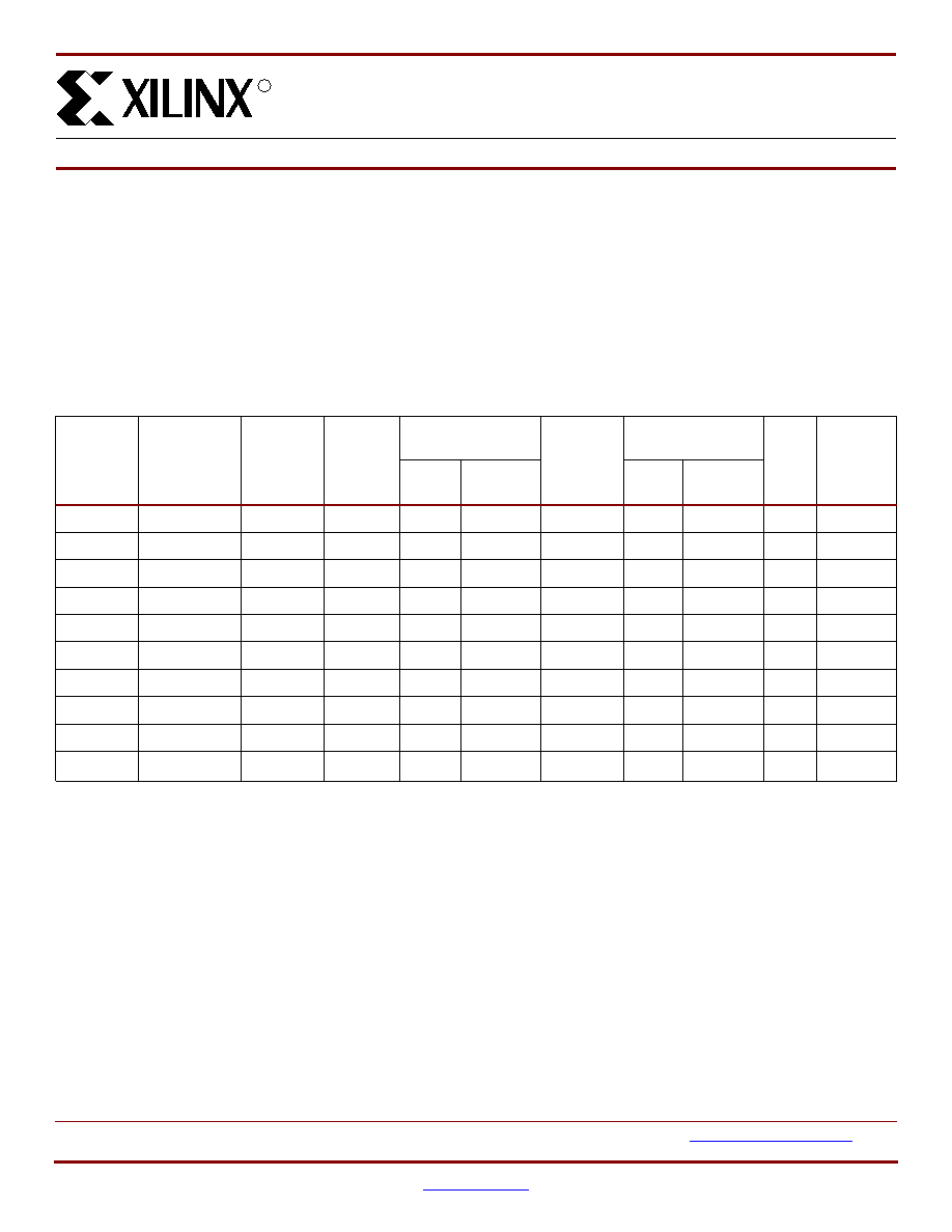
Virtex-II Pro family members and resources are shown in
Table 1
.
RocketIO Transceiver Features
∑
Full-Duplex Serial Transceiver (SERDES) Capable of
Baud Rates from 600 Mb/s to 3.125 Gb/s
∑
120 Gb/s Duplex Data Rate (24 Channels)
∑
Monolithic Clock Synthesis and Clock Recovery (CDR)
∑
Fibre Channel, 10G Fibre Channel, Gigabit Ethernet,
10 Gb Attachment Unit Interface (XAUI), and
Infiniband-Compliant Transceivers
∑
8-, 16-, or 32-bit Selectable Internal FPGA Interface
∑
8B /10B Encoder and Decoder (optional)
∑
50
/75 on-chip Selectable Transmit and Receive
Terminations
∑
Programmable Comma Detection
∑
Channel Bonding Support (from 2 to 24 Channels)
∑
Rate Matching via Insertion/Deletion Characters
∑
Four Levels of Selectable Pre-Emphasis
∑
Five Levels of Output Differential Voltage
∑
Per-Channel Internal Loopback Modes
∑
2.5V Transceiver Supply Voltage
0
8
Virtex-II ProTM Platform FPGAs:
Introduction and Overview
DS083-1 (v2.4.2) August 25, 2003
0
0
Advance Product Specification
R
Table 1: Virtex-II Pro FPGA Family Members
Device
RocketIO
Transceiver
Blocks
PowerPC
Processor
Blocks
Logic
Cells
(1)
CLB (1 = 4 slices =
max 128 bits)
18 X 18 Bit
Multiplier
Blocks
Block SelectRAM+
DCMs
Maximum
User
I/O Pads
Slices
Max Distr
RAM (Kb)
18 Kb
Blocks
Max Block
RAM (Kb)
XC2VP2
4
0
3,168
1,408
44
12
12
216
4
204
XC2VP4
4
1
6,768
3,008
94
28
28
504
4
348
XC2VP7
8
1
11,088
4,928
154
44
44
792
4
396
XC2VP20
8
2
20,880
9,280
290
88
88
1,584
8
564
XC2VP30
8
2
30,816
13,696
428
136
136
2,448
8
644
XC2VP40
0
(2)
or 12
2
43,632
19,392
606
192
192
3,456
8
804
XC2VP50
0
(2)
or 16
2
53,136
23,616
738
232
232
4,176
8
852
XC2VP70
16 or 20
2
74,448
33,088
1,034
328
328
5,904
8
996
XC2VP100
0
(2)
or 20
2
99,216
44,096
1,378
444
444
7,992
12
1,164
XC2VP125
0
(2)
, 20, or 24
4
125,136
55,616
1,738
556
556
10,008
12
1,200
Notes:
1.
Logic Cell = (1) 4-input LUT + (1)FF + Carry Logic
2.
These devices can be ordered in a configuration without RocketIO transceivers. See
Table 3
for package configurations.

General Description
R
2
www.xilinx.com
DS083-1 (v2.4.2) August 25, 2003
1-800-255-7778
Advance Product Specification
PowerPC RISC Block Features
∑
Embedded 300+ MHz Harvard Architecture Block
∑
Low Power Consumption: 0.9 mW/MHz
∑
Five-Stage Data Path Pipeline
∑
Hardware Multiply/Divide Unit
∑
Thirty-Two 32-bit General Purpose Registers
∑
16 KB Two-Way Set-Associative Instruction Cache
∑
16 KB Two-Way Set-Associative Data Cache
∑
Memory Management Unit (MMU)
-
64-entry unified Translation Look-aside Buffers (TLB)
-
Variable page sizes (1 KB to 16 MB)
∑
Dedicated On-Chip Memory (OCM) Interface
∑
Supports IBM CoreConnectTM Bus Architecture
∑
Debug and Trace Support
∑
Timer Facilities
Virtex-II Pro Platform FPGA Technology
∑
SelectRAM+ Memory Hierarchy
-
Up to 10 Mb of True Dual-Port RAM in 18 Kb block
SelectRAM+ resources
-
Up to 1,738 Kb of distributed SelectRAM+
resources
-
High-performance interfaces to external memory
∑
Arithmetic Functions
-
Dedicated 18-bit x 18-bit multiplier blocks
-
Fast look-ahead carry logic chains
∑
Flexible Logic Resources
-
Up to 111,232 internal registers/latches with Clock
Enable
-
Up to 111,232 look-up tables (LUTs) or cascadable
variable (1 to 16 bits) shift registers
-
Wide multiplexers and wide-input function support
-
Horizontal cascade chain and Sum-of-Products
support
-
Internal 3-state busing
∑
High-Performance Clock Management Circuitry
-
Up to twelve Digital Clock Manager (DCM) modules
∑
Precise clock de-skew
∑
Flexible frequency synthesis
∑
High-resolution phase shifting
-
16 global clock multiplexer buffers in all parts
∑
Active Interconnect Technology
-
Fourth-generation segmented routing structure
-
Fast, predictable routing delay, independent of
fanout
-
Deep sub-micron noise immunity benefits
∑
SelectIOTM-Ultra Technology
-
Up to 1,200 user I/Os
-
Twenty-two single-ended standards and
six differential standards
-
Programmable LVCMOS sink/source current (2 mA
to 24 mA) per I/O
-
XCITE Digitally Controlled Impedance (DCI) I/O
-
PCI/ PCI-X support
(1)
-
Differential signaling
∑
840 Mb/s Low-Voltage Differential Signaling I/O
(LVDS) with current mode drivers
∑
Bus LVDS I/O
∑
HyperTransport (LDT) I/O with current driver
buffers
∑
Built-in DDR input and output registers
-
Proprietary high-performance SelectLink
technology for communications between Xilinx
devices
∑
High-bandwidth data path
∑
Double Data Rate (DDR) link
∑
Web-based HDL generation methodology
∑
SRAM-Based In-System Configuration
-
Fast SelectMAPTM configuration
-
Triple Data Encryption Standard (DES) security
option (bitstream encryption)
-
IEEE 1532 support
-
Partial reconfiguration
-
Unlimited reprogrammability
-
Readback capability
∑
Supported by Xilinx FoundationTM and Alliance
SeriesTM Development Systems
-
Integrated VHDL and Verilog design flows
-
ChipScopeTM Integrated Logic Analyzer
∑
0.13 µm Nine-Layer Copper Process with 90 nm
High-Speed Transistors
∑
1.5V (V
CCINT
) core power supply, dedicated 2.5V
V
CCAUX
auxiliary and V
CCO
I/O power supplies
∑
IEEE 1149.1 Compatible Boundary-Scan Logic Support
∑
Flip-Chip and Wire-Bond Ball Grid Array (BGA)
Packages in Standard 1.00 mm Pitch
∑
Each Device 100% Factory Tested
General Description
The Virtex-II Pro family contains platform FPGAs for
designs that are based on IP cores and customized mod-
ules. The family incorporates multi-gigabit transceivers and
PowerPC CPU blocks in Virtex-II Pro Series FPGA architec-
ture. It empowers complete solutions for telecommunica-
tion, wireless, networking, video, and DSP applications.
The leading-edge 0.13 µm CMOS nine-layer copper pro-
cess and Virtex-II Pro architecture are optimized for high
performance designs in a wide range of densities. Combin-
ing a wide variety of flexible features and IP cores, the
Virtex-II Pro family enhances programmable logic design
capabilities and is a powerful alternative to mask-pro-
grammed gate arrays.
1. Refer to
XAPP653
for more information.

Virtex-II ProTM Platform FPGAs: Introduction and Overview
R
DS083-1 (v2.4.2) August 25, 2003
www.xilinx.com
3
Advance Product Specification
1-800-255-7778
Architecture
Virtex-II Pro Array Overview
Virtex-II Pro devices are user-programmable gate arrays
with various configurable elements and embedded blocks
optimized for high-density and high-performance system
designs. Virtex-II Pro devices implement the following func-
tionality:
∑
Embedded high-speed serial transceivers enable data
bit rate up to 3.125 Gb/s per channel.
∑
Embedded IBM PowerPC 405 RISC processor blocks
provide performance of 300+ MHz.
∑
SelectIO-Ultra blocks provide the interface between
package pins and the internal configurable logic. Most
popular and leading-edge I/O standards are supported
by the programmable IOBs.
∑
Configurable Logic Blocks (CLBs) provide functional
elements for combinatorial and synchronous logic,
including basic storage elements. BUFTs (3-state
buffers) associated with each CLB element drive
dedicated segmentable horizontal routing resources.
∑
Block SelectRAM+ memory modules provide large
18 Kb storage elements of True Dual-Port RAM.
∑
Embedded multiplier blocks are 18-bit x 18-bit
dedicated multipliers.
∑
Digital Clock Manager (DCM) blocks provide
self-calibrating, fully digital solutions for clock
distribution delay compensation, clock multiplication
and division, and coarse- and fine-grained clock phase
shifting.
A new generation of programmable routing resources called
Active Interconnect Technology interconnects all of these
elements. The general routing matrix (GRM) is an array of
routing switches. Each programmable element is tied to a
switch matrix, allowing multiple connections to the general
routing matrix. The overall programmable interconnection is
hierarchical and designed to support high-speed designs.
All programmable elements, including the routing
resources, are controlled by values stored in static memory
cells. These values are loaded in the memory cells during
configuration and can be reloaded to change the functions
of the programmable elements.
Virtex-II Pro Features
This section briefly describes Virtex-II Pro features. For
more details, refer to
Virtex-II ProTM Platform FPGAs: Func-
tional Description
.
RocketIO Multi-Gigabit Transceivers
The RocketIO Multi-Gigabit Transceiver, based on Mind-
speed's SkyRail technology, is a flexible parallel-to-serial
and serial-to-parallel embedded transceiver used for
high-bandwidth interconnection between buses, back-
planes, or other subsystems.
Multiple user instantiations in an FPGA are possible, provid-
ing up to 120 Gb/s of full-duplex raw data transfer. Each
channel can be operated at a maximum data transfer rate of
3.125 Gb/s.
Each RocketIO transceiver implements:
∑
Serializer and deserializer (SERDES)
∑
Monolithic clock synthesis and clock recovery (CDR)
∑
Fibre Channel, 10G Fibre Channel, Gigabit Ethernet,
XAUI, and Infiniband-compliant transceivers
∑
8-, 16-, or 32-bit selectable FPGA interface
∑
8B/10B encoder and decoder with bypassing option on
each channel
∑
Channel bonding support (2 to 24 channels)
-
Elastic buffers for inter-chip deskewing and
channel-to-channel alignment
∑
Receiver clock recovery tolerance of up to
75 non-transitioning bits
∑
50
/75 on-chip selectable transmit and receive
terminations
∑
Programmable comma detection
∑
Rate matching via insertion/deletion characters
∑
Automatic lock-to-reference function
∑
Optional transmit and receive data inversion
∑
Four levels of pre-emphasis support
∑
Per-channel serial and parallel transmitter-to-receiver
internal loopback modes
∑
Cyclic Redundancy Check (CRC) support
PowerPC 405 Processor Block
The PPC405 RISC CPU can execute instructions at a sus-
tained rate of one instruction per cycle. On-chip instruction
and data cache reduce design complexity and improve sys-
tem throughput.
The PPC405 features include:
∑
PowerPC RISC CPU
-
Implements the PowerPC User Instruction Set
Architecture (UISA) and extensions for embedded
applications
-
Thirty-two 32-bit general purpose registers (GPRs)
-
Static branch prediction
-
Five-stage pipeline with single-cycle execution of
most instructions, including loads/stores
-
Unaligned and aligned load/store support to cache,
main memory, and on-chip memory
-
Hardware multiply/divide for faster integer
arithmetic (4-cycle multiply, 35-cycle divide)
-
Enhanced string and multiple-word handling
-
Big/little endian operation support
∑
Storage Control
-
Separate instruction and data cache units, both
two-way set-associative and non-blocking
-
Eight words (32 bytes) per cache line
Architecture
R
4
www.xilinx.com
DS083-1 (v2.4.2) August 25, 2003
1-800-255-7778
Advance Product Specification
-
16 KB array Instruction Cache Unit (ICU), 16 KB
array Data Cache Unit (DCU)
-
Operand
forwarding during instruction cache line fill
-
Copy-back or write-through DCU strategy
-
Doubleword instruction fetch from cache improves
branch latency
∑
Virtual mode memory management unit (MMU)
-
Translation of the 4 GB logical address space into
physical addresses
-
Software control of page replacement strategy
-
Supports multiple simultaneous page sizes ranging
from 1 KB to 16 MB
∑
OCM controllers provide dedicated interfaces between
Block SelectRAM+ memory and processor block
instruction and data paths for high-speed access
∑
PowerPC timer facilities
-
64-bit time base
-
Programmable interval timer (PIT)
-
Fixed interval timer (FIT)
-
Watchdog timer (WDT)
∑
Debug Support
-
Internal debug mode
-
External debug mode
-
Debug Wait mode
-
Real Time Trace debug mode
-
Enhanced debug support with logical operators
-
Instruction trace and trace-back support
-
Forward or backward trace
∑
Two hardware interrupt levels support
∑
Advanced power management support
Input/Output Blocks (IOBs)
IOBs are programmable and can be categorized as follows:
∑
Input block with an optional single data rate (SDR) or
double data rate (DDR) register
∑
Output block with an optional SDR or DDR register and
an optional 3-state buffer to be driven directly or
through an SDR or DDR register
∑
Bidirectional block (any combination of input and output
configurations)
These registers are either edge-triggered D-type flip-flops
or level-sensitive latches.
IOBs support the following single-ended I/O standards:
∑
LVTTL, LVCMOS (3.3V, 2.5V, 1.8V, and 1.5V)
(1)
∑
PCI-X compatible (133 MHz and 66 MHz) at 3.3V
(2)
∑
PCI compliant (66 MHz and 33 MHz) at 3.3V
(2)
∑
GTL and GTLP
∑
HSTL (1.5V and 1.8V, Class I, II, III, and IV)
∑
SSTL (1.8V and 2.5V, Class I and II)
The DCI I/O feature automatically provides on-chip termina-
tion for each single-ended I/O standard.
The IOB elements also support the following differential sig-
naling I/O standards:
∑
LVDS and Extended LVDS (2.5V)
∑
BLVDS (Bus LVDS)
∑
ULVDS
∑
LDT
∑
LVPECL (2.5V)
Two adjacent pads are used for each differential pair. Two or
four IOB blocks connect to one switch matrix to access the
routing resources.
Configurable Logic Blocks (CLBs)
CLB resources include four slices and two 3-state buffers.
Each slice is equivalent and contains:
∑
Two function generators (F & G)
∑
Two storage elements
∑
Arithmetic logic gates
∑
Large multiplexers
∑
Wide function capability
∑
Fast carry look-ahead chain
∑
Horizontal cascade chain (OR gate)
The function generators F & G are configurable as 4-input
look-up tables (LUTs), as 16-bit shift registers, or as 16-bit
distributed SelectRAM+ memory.
In addition, the two storage elements are either
edge-triggered D-type flip-flops or level-sensitive latches.
Each CLB has internal fast interconnect and connects to a
switch matrix to access general routing resources.
Block SelectRAM+ Memory
The block SelectRAM+ memory resources are 18 Kb of
True Dual-Port RAM, programmable from 16K x 1 bit to
512 x 36 bit, in various depth and width configurations.
Each port is totally synchronous and independent, offering
three "read-during-write" modes. Block SelectRAM+ mem-
ory is cascadable to implement large embedded storage
blocks. Supported memory configurations for dual-port and
single-port modes are shown in
Table 2
.
18 X 18 Bit Multipliers
A multiplier block is associated with each SelectRAM+
memory block. The multiplier block is a dedicated
18 x 18-bit 2s complement signed multiplier, and is opti-
1. Refer to
XAPP659
for more information.
2. Refer to
XAPP653
for more information.
Table 2: Dual-Port and Single-Port Configurations
16K x 1 bit
4K x 4 bits
1K x 18 bits
8K x 2 bits
2K x 9 bits
512 x 36 bits

Virtex-II ProTM Platform FPGAs: Introduction and Overview
R
DS083-1 (v2.4.2) August 25, 2003
www.xilinx.com
5
Advance Product Specification
1-800-255-7778
mized for operations based on the block SelectRAM+ con-
tent on one port. The 18 x 18 multiplier can be used
independently of the block SelectRAM+ resource.
Read/multiply/accumulate operations and DSP filter struc-
tures are extremely efficient.
Both the SelectRAM+ memory and the multiplier resource
are connected to four switch matrices to access the general
routing resources.
Global Clocking
The DCM and global clock multiplexer buffers provide a
complete solution for designing high-speed clock schemes.
Up to twelve DCM blocks are available. To generate
deskewed internal or external clocks, each DCM can be
used to eliminate clock distribution delay. The DCM also
provides 90-, 180-, and 270-degree phase-shifted versions
of its output clocks. Fine-grained phase shifting offers
high-resolution phase adjustments in increments of
1
/
256
of
the clock period. Very flexible frequency synthesis provides
a clock output frequency equal to a fractional or integer mul-
tiple of the input clock frequency. For exact timing parame-
ters, see
Virtex-II ProTM Platform FPGAs: DC and Switching
Characteristics
.
Virtex-II Pro devices have 16 global clock MUX buffers, with
up to eight clock nets per quadrant. Each clock MUX buffer
can select one of the two clock inputs and switch glitch-free
from one clock to the other. Each DCM can send up to four
of its clock outputs to global clock buffers on the same edge.
Any global clock pin can drive any DCM on the same edge.
Routing Resources
The IOB, CLB, block SelectRAM+, multiplier, and DCM ele-
ments all use the same interconnect scheme and the same
access to the global routing matrix. Timing models are
shared, greatly improving the predictability of the perfor-
mance of high-speed designs.
There are a total of 16 global clock lines, with eight available
per quadrant. In addition, 24 vertical and horizontal long
lines per row or column, as well as massive secondary and
local routing resources, provide fast interconnect.
Virtex-II Pro buffered interconnects are relatively unaffected
by net fanout, and the interconnect layout is designed to
minimize crosstalk.
Horizontal and vertical routing resources for each row or
column include:
∑
24 long lines
∑
120 hex lines
∑
40 double lines
∑
16 direct connect lines (total in all four directions)
Boundary Scan
Boundary-scan instructions and associated data registers
support a standard methodology for accessing and config-
uring Virtex-II Pro devices, complying with IEEE standards
1149.1 and 1532. A system mode and a test mode are
implemented. In system mode, a Virtex-II Pro device will
continue to function while executing non-test bound-
ary-scan instructions. In test mode, boundary-scan test
instructions control the I/O pins for testing purposes. The
Virtex-II Pro Test Access Port (TAP) supports BYPASS,
PRELOAD, SAMPLE, IDCODE, and USERCODE non-test
instructions. The EXTEST, INTEST, and HIGHZ test instruc-
tions are also supported.
Configuration
Virtex-II Pro devices are configured by loading the bitstream
into internal configuration memory using one of the follow-
ing modes:
∑
Slave-serial mode
∑
Master-serial mode
∑
Slave SelectMAP mode
∑
Master SelectMAP mode
∑
Boundary-Scan mode (IEEE 1532)
A Data Encryption Standard (DES) decryptor is available
on-chip to secure the bitstreams. One or two triple-DES key
sets
can
be
used
to
optionally
encrypt
the
configuration
data.
The Xilinx System Advanced Configuration Enviornment
(System ACE) family offers high-capacity and flexible solu-
tion for FPGA configuration as well as program/data storage
for the processor. See
DS080
, System ACE CompactFlash
Solution for more information.
Readback and Integrated Logic Analyzer
Configuration data stored in Virtex-II Pro configuration
memory can be read back for verification. Along with the
configuration data, the contents of all flip-flops/latches, dis-
tributed SelectRAM+, and block SelectRAM+ memory
resources can be read back. This capability is useful for
real-time debugging.
The Xilinx ChipScope Integrated Logic Analyzer (ILA) cores
and Integrated Bus Analyzer (IBA) cores, along with the
ChipScope Pro Analyzer software, provide a complete solu-
tion for accessing and verifying user designs within
Virtex-II Pro devices.
IP Core and Reference Support
R
6
www.xilinx.com
DS083-1 (v2.4.2) August 25, 2003
1-800-255-7778
Advance Product Specification
IP Core and Reference Support
Intellectual Property is part of the Platform FPGA solution.
In addition to the existing FPGA fabric cores, the list below
shows some of the currently available hardware and soft-
ware intellectual properties specially developed for
Virtex-II Pro by Xilinx. Each IP core is modular, portable,
Real-Time Operating System (RTOS) independent, and
CoreConnect compatible for ease of design migration.
Refer to
www.xilinx.com/ipcenter
for the latest and most
complete list of cores.
Hardware Cores
∑
Bus Infrastructure cores (arbiters, bridges, and more)
∑
Memory cores (DDR, Flash, and more)
∑
Peripheral cores (UART, IIC, and more)
∑
Networking cores (ATM, Ethernet, and more)
Software Cores
∑
Boot code
∑
Test code
∑
Device drivers
∑
Protocol stacks
∑
RTOS integration
∑
Customized board support package
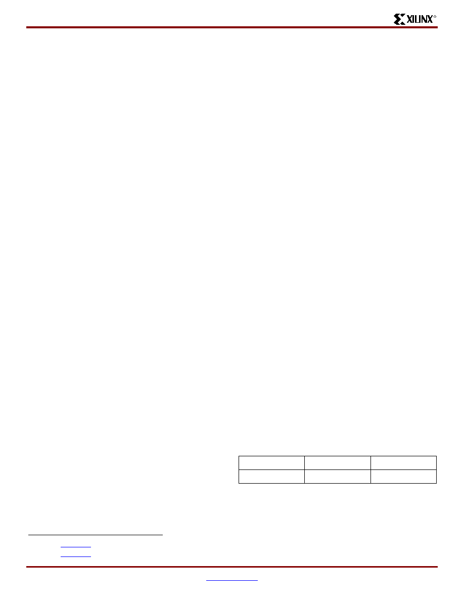
Virtex-II Pro Device/Package
Combinations and Maximum I/Os
Offerings include ball grid array (BGA) packages with
1.0 mm pitch. In addition to traditional wire-bond intercon-
nects, flip-chip interconnect is used in some of the BGA
offerings. The use of flip-chip interconnect offers more I/Os
than are possible in wire-bond versions of the similar pack-
ages. Flip-chip construction offers the combination of high
pin count and excellent power dissipation.
The Virtex-II Pro device/package combination table
(
Table 3
) details the maximum number of user I/Os and
RocketIO transceivers for each device and package using
wire-bond or flip-chip technology.
∑
FG denotes Wirebond fine-pitch BGA (1.00 mm pitch).
∑
FF denotes FlipChip fine-pitch BGA (1.00 mm pitch).
The FF1148 and FF1696 packages have no RocketIO
transceivers bonded out. Extra SelectIO-Ultra resources
occupy available pins in these packages, resulting in a
higher user I/O count. FF1148 and FF1696 packages are
available for the XC2VP40, XC2VP50, XC2VP100, and
XC2VP125 devices only.
The I/Os per package count includes all user I/Os except
the 15 control pins (CCLK, DONE, M0, M1, M2, PROG_B,
PWRDWN_B, TCK, TDI, TDO, TMS, HSWAP_EN, DXN,
DXP, and RSVD), VBATT, and RocketIO transceiver pins.
Table 3: Virtex-II Pro Device/Package Combinations and Maximum Number of Available I/Os
Pkg
Pitch
(mm)
Size
(mm)
Available User I/Os / Available RocketIO Transceivers
XC2VP2 XC2VP4 XC2VP7 XC2VP20 XC2VP30 XC2VP40 XC2VP50 XC2VP70 XC2VP100
XC2VP125
FG256
1.00
17 x 17
140 / 4
140 / 4
FG456
1.00
23 x 23
156 / 4
248 / 4
248 / 8
FG676
1.00
26 x 26
404 / 8
416 / 8
416 / 8
FF672
1.00
27 x 27
204 / 4
348 / 4
396 / 8
FF896
1.00
31 x 31
396 / 8
556 / 8
556 / 8
FF1152
1.00
35 x 35
564 / 8
644 / 8
692 / 12
692 / 16
FF1148
1.00
35 x 35
804 / 0
(1)
812 / 0
(1)
FF1517
1.00
40 x 40
852 / 16
964 / 16
FF1704
1.00
42.5 x
42.5
996 / 20
1,040 / 20
1,040 / 20
FF1696
1.00
42.5 x
42.5
1,164 / 0
(1)
1,200 / 0
(1)
Notes:
1.
The RocketIO transceivers in devices in the FF1148 and FF1696 packages are not bonded out to the package pins.
2.
Consult Xilinx for package options supporting 24 RocketIO transceivers.
Virtex-II ProTM Platform FPGAs: Introduction and Overview
R
DS083-1 (v2.4.2) August 25, 2003
www.xilinx.com
7
Advance Product Specification
1-800-255-7778
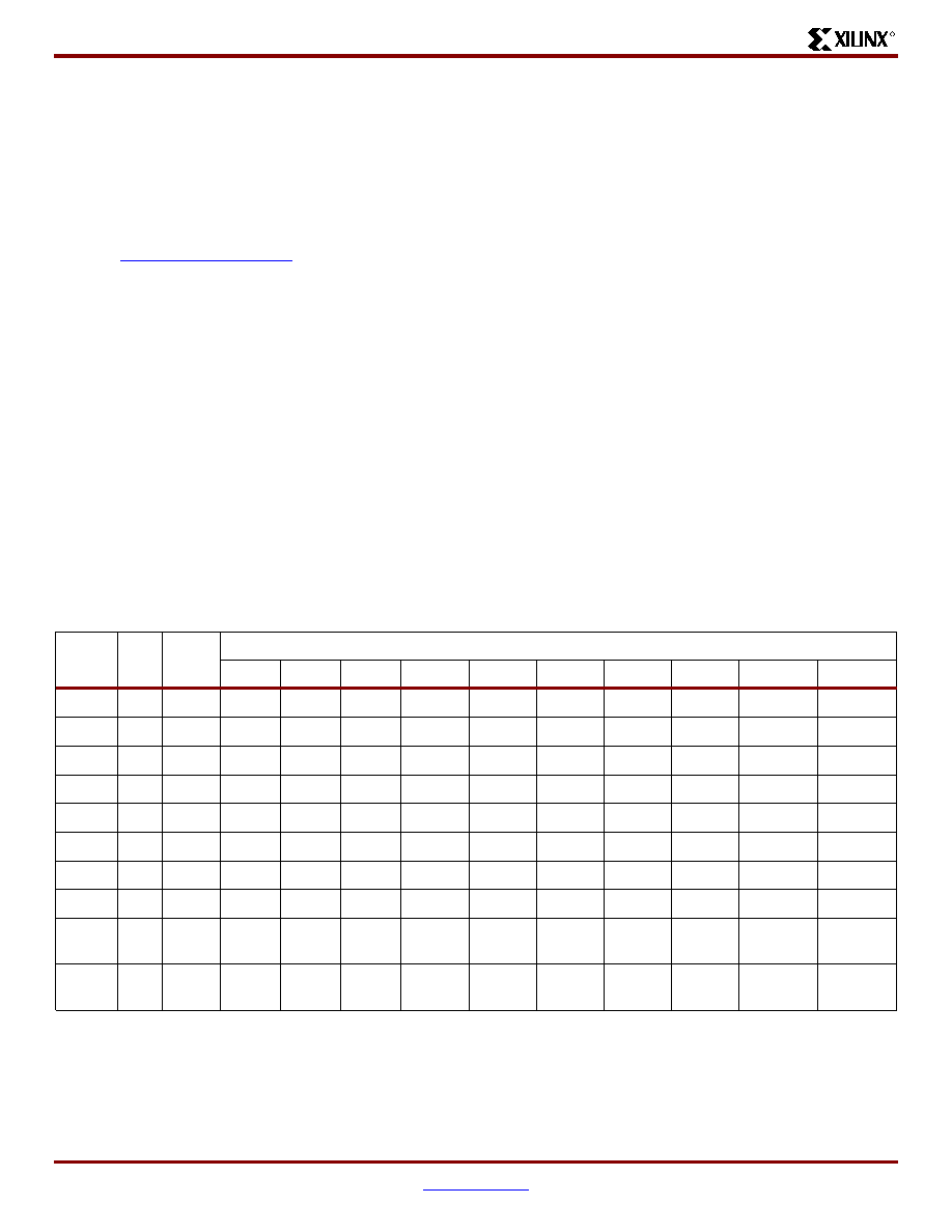
Maximum Performance
Maximum RocketIO transceiver and PowerPC processor block performance varies, depending on the package style and
speed grade. See
Table 4
for details.
Virtex-II ProTM Platform FPGAs: DC and Switching Characteristics
contains the rest of
the FPGA fabric performance parameters.
Virtex-II Pro Ordering Information
Virtex-II Pro ordering information is shown in
Figure 1
.
Revision History
This section records the change history for this module of the data sheet.
Table 4: Maximum RocketIO Transceiver and Processor Block Performance
Speed Grade
Units
-7
-6
-5
RocketIO Transceiver Wirebond (FG)
2.5
2.5
2.0
Gb/s
RocketIO Transceiver FlipChip (FF)
3.125
3.125
2.0
Gb/s
PowerPC Processor Block
400
350
300
MHz
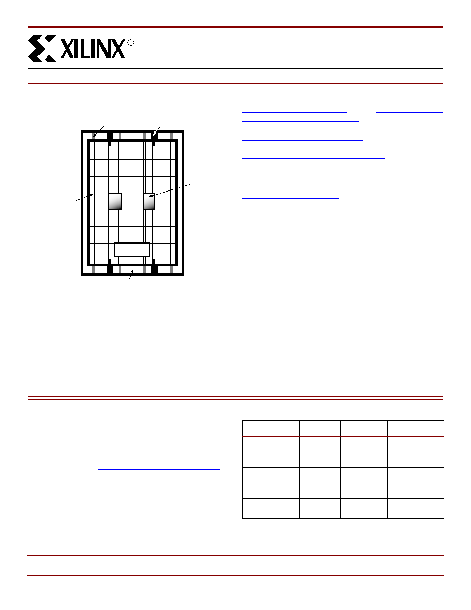
Figure 1: Virtex-II Pro Ordering Information
Date
Version
Revision
01/31/02
1.0
Initial Xilinx release.
06/13/02
2.0
New Virtex-II Pro family members. New timing parameters per speedsfile v1.62.
09/03/02
2.1
Updates to
Table 1
and
Table 3
. Processor Block information added to
Table 4
.
09/27/02
2.2
In
Table 1
, correct max number of XC2VP30 I/Os to 644.
11/20/02
2.3
Add bullet items for 3.3V I/O features.
01/20/03
2.4
∑
In
Table 3
, add FG676 package option for XC2VP20, XC2VP30, and XC2VP40.
∑
Remove FF1517 package option for XC2VP40.
03/24/03
2.4.1
∑
Correct number of single-ended I/O standards from 19 to 22.
∑
Correct minimum RocketIO serial speed from 622 Mbps to 600 Mbps.
08/25/03
2.4.2
∑
Add footnote referring to XAPP659 to callout for 3.3V I/O standards on page 4.
Example: XC2VP7-7FG456C
Device Type
Temperature Range:
C = Commercial (Tj = 0∞C to +85∞C)
I = Industrial (Tj = -40∞C to +100∞C)
Number of Pins
Package Type
Speed Grade
(-5, -6, -7)
DS083_02_052902

Virtex-II Pro Data Sheet
R
8
www.xilinx.com
DS083-1 (v2.4.2) August 25, 2003
1-800-255-7778
Advance Product Specification
Virtex-II Pro Data Sheet
The Virtex-II Pro Data Sheet contains the following modules:
∑
Virtex-II ProTM Platform FPGAs: Introduction and
Overview (Module 1)
∑
Virtex-II ProTM Platform FPGAs: Functional Description
(Module 2)
∑
Virtex-II ProTM Platform FPGAs: DC and Switching
Characteristics (Module 3)
∑
Virtex-II ProTM Platform FPGAs: Pinout Information
(Module 4)
© 2003 Xilinx, Inc. All rights reserved. All Xilinx trademarks, registered trademarks, patents, and disclaimers are as listed at
http://www.xilinx.com/legal.htm
.
All other trademarks and registered trademarks are the property of their respective owners. All specifications are subject to change without notice.
DS083-2 (v2.9) October 14, 2003
www.xilinx.com
1
Advance Product Specification
1-800-255-7778
Virtex-II Pro Array Functional Description
This module describes the following Virtex-II Pro functional
components, as shown in
Figure 1
:
∑
Embedded RocketIOTM Multi-Gigabit Transceiver (MGT)
∑
Processor block with embedded IBM
Æ
PowerPCTM 405
RISC CPU core (PPC405) and integration circuitry.
∑
FPGA fabric based on Virtex-II architecture.
For a description of PPC405 embedded core programming
models and internal core operations, refer to the
PowerPC
Processor Reference Guide
and the
PowerPC 405 Pro-
cessor Block Reference Guide
. For detailed RocketIO
transceiver digital/ analog design considerations, refer to
RocketIO Transceiver User Guide
. For a detailed descrip-
tion of the FPGA fabric (CLB, IOB, DCM, etc.), refer to the
Virtex-II Pro Platform FPGA User Guide
.
All of the documents above, as well as a complete listing
and description of Xilinx-developed Intellectual Property
cores for Virtex-II Pro, are available on the Xilinx website at
www.xilinx.com/virtex2pro
.
Virtex-II Pro Compared to Virtex-II Devices
Virtex-II Pro devices are built on the Virtex-II FPGA archi-
tecture. Most FPGA features are identical to Virtex-II
devices. Differences are described below:
∑
The Virtex-II Pro FPGA family is the first to incorporate
embedded PPC405 cores and RocketIO MGTs.
∑
V
CCAUX
, the auxiliary supply voltage, is 2.5V instead of
3.3V as for Virtex-II devices. Advanced processing at
0.13
µm has resulted in a smaller die, faster speed,
and lower power consumption.
∑
Virtex-II Pro devices are neither bitstream-compatible nor
pin-compatible with Virtex-II devices. However, Virtex-II
designs can be compiled into Virtex-II Pro devices.
∑
SSTL3, AGP-2X/AGP, LVPECL_33, LVDS_33, and
LVDSEXT_33 standards are not supported.
∑
The open-drain output pin TDO does not have an
internal pullup resistor.
Functional Description: RocketIO
Multi-Gigabit Transceiver (MGT)
This section summarizes the features of the RocketIO
multi-gigabit transceiver. For an in-depth discussion of the
RocketIO MGT, including digital and analog design consid-
erations, refer to the
RocketIO Transceiver User Guide
.
Overview
The embedded RocketIO multi-gigabit transceiver is based
on Mindspeed's SkyRailTM technology. Up to twenty-four
transceivers are available. The transceiver is designed to
operate at any baud rate in the range of 622 Mb/s to
3.125 Gb/s per channel. This includes specific baud rates
used by various standards as listed in
Table 1
.
0
48
Virtex-II ProTM Platform FPGAs:
Functional Description
DS083-2 (v2.9) October 14, 2003
0
0
Advance Product Specification
R
Figure 1: Virtex-II Pro Generic Architecture Overview
CLB
Multipliers and
Block SelectRAM
Processor Block
Configurable
Logic
SelectIOTM-Ultra
DS083-1_01_010802
DCM
RocketIOTM
Multi-Gigabit Transceiver
CLB
CLB
CLB
Table 1: Protocols Supported by RocketIO Transceiver
Protocol
Channels
(Lanes)
I/O Baud Rate
(Gb/s)
Reference Clock
Rate (MHz)
Fibre Channel
1
1.06
53
2.12
106
3.1875
(1)
159.375
Gigabit Ethernet
1
1.25
62.5
10Gbit Ethernet
4
3.125
156.25
Infiniband
1, 4, 12
2.5
125
Aurora
1, 2, 3, 4, ...
0.840 ≠ 3.125
42.00 ≠ 156.25
Custom Protocol
1, 2, 3, 4, ...
up to 3.125
up to 156.25
Notes:
1.
Virtex-II Pro MGT can support the 10G Fibre Channel data rates of
3.1875 Gb/s across 6" of standard FR-4 PCB and one connector
(Molex 74441 or equivalent) with a bit error rate of 10
-12
or better.

Functional Description: RocketIO Multi-Gigabit Transceiver (MGT)
R
2
www.xilinx.com
DS083-2 (v2.9) October 14, 2003
1-800-255-7778
Advance Product Specification
The serial bit rate need not be configured in the transceiver,
as the operating frequency is implied by the received data
and reference clock applied.
The RocketIO transceiver consists of the Physical Media
Attachment (PMA) and Physical Coding Sublayer (PCS).
The PMA contains the serializer and deserializer. The
PCS
contains
the
bypassable
8B/10B encoder/ decoder, elastic
buffers, and Cyclic Redundancy Check (CRC) units. The
encoder and decoder handle the 8B/10B coding scheme.
The elastic buffers support the clock correction (rate match-
ing) and channel bonding features. The CRC units perform
CRC generation and checking.
Figure 2
shows a high-level block diagram of the RocketIO
transceiver and its FPGA interface signals.
Figure 2: RocketIO Transceiver Block Diagram
FPGA FABRIC
MULTI-GIGABIT TRANSCEIVER CORE
Serializer
RXP
TXP
Clock
Manager
Power Down
PACKAGE
PINS
Deserializer
Comma
Detect
Realign
8B/10B
Decoder
TX
FIFO
CRC
Check
CRC
Channel Bonding
and
Clock Correction
CHBONDI[3:0]
CHBONDO[3:0]
8B/10B
Encoder
RX
Elastic
Buffer
Output
Polarity
RXN
GNDA
TXN
DS083-2_04_090402
POWERDOWN
RXRECCLK
RXPOLARITY
RXREALIGN
RXCOMMADET
RXRESET
RXCLKCORCNT
RXLOSSOFSYNC
RXDATA[15:0]
RXDATA[31:16]
RXCHECKINGCRC
RXCRCERR
RXNOTINTABLE[3:0]
RXDISPERR[3:0]
RXCHARISK[3:0]
RXCHARISCOMMA[3:0]
RXRUNDISP[3:0]
RXBUFSTATUS[1:0]
ENCHANSYNC
RXUSRCLK
RXUSRCLK2
CHBONDDONE
TXBUFERR
TXDATA[15:0]
TXDATA[31:16]
TXBYPASS8B10B[3:0]
TXCHARISK[3:0]
TXCHARDISPMODE[3:0]
TXCHARDISPVAL[3:0]
TXKERR[3:0]
TXRUNDISP[3:0]
TXPOLARITY
TXFORCECRCERR
TXINHIBIT
LOOPBACK[1:0]
TXRESET
REFCLK
REFCLK2
REFCLKSEL
ENPCOMMAALIGN
ENMCOMMAALIGN
TXUSRCLK
TXUSRCLK2
VTRX
AVCCAUXRX
VTTX
AVCCAUXTX
2.5V RX
TX/RX GND
Termination Supply RX
2.5V TX
Termination Supply TX
Serial Loopback Path
Parallel Loopback Path
BREFCLK
BREFCLK2

Virtex-II ProTM Platform FPGAs: Functional Description
R
DS083-2 (v2.9) October 14, 2003
www.xilinx.com
3
Advance Product Specification
1-800-255-7778
Clock Synthesizer
Synchronous serial data reception is facilitated by a
clock/data recovery circuit. This circuit uses a fully mono-
lithic Phase Lock Loop (PLL), which does not require any
external components. The clock/data recovery circuit
extracts both phase and frequency from the incoming data
stream. The recovered clock is presented on output
RXRECCLK at 1/20 of the serial received data rate.
The gigabit transceiver multiplies the reference frequency
provided on the reference clock input (REFCLK) by 20. The
multiplication of the clock is achieved by using a fully mono-
lithic PLL that does not require any external components.
No fixed phase relationship is assumed between REFCLK,
RXRECCLK, and/or any other clock that is not tied to either
of these clocks. When the 4-byte or 1-byte receiver data
path is used, RXUSRCLK and RXUSRCLK2 have different
frequencies, and each edge of the slower clock is aligned to
a falling edge of the faster clock. The same relationships
apply to TXUSRCLK and TXUSRCLK2.
Clock and Data Recovery
The clock/data recovery (CDR) circuits will lock to the refer-
ence clock automatically if the data is not present. For
proper operation, the frequency of the reference clock must
be within
±
100 ppm of the nominal frequency.
It is critical to keep power supply noise low in order to mini-
mize common and differential noise modes into the
clock/data recovery circuitry. Refer to the RocketIO Trans-
ceiver User Guide for more details.
Transmitter
FPGA Transmit Interface
The FPGA can send either one, two, or four characters of
data to the transmitter. Each character can be either 8 bits
or 10 bits wide. If 8-bit data is applied, the additional inputs
become control signals for the 8B/10B encoder. When the
8B/10B encoder is bypassed, the 10-bit character order is
generated as follows:
TXCHARDISPMODE[0]
(first bit transmitted)
TXCHARDISPVAL[0]
TXDATA[7:0]
(last bit transmitted is TXDATA[0])
8B/10B Encoder
A bypassable 8B/10B encoder is included. The encoder
uses the same 256 data characters and 12 control charac-
ters that are used for Gigabit Ethernet, Fibre Channel, and
InfiniBand.
The encoder accepts 8 bits of data along with a K-character
signal for a total of 9 bits per character applied, and
generates a 10 bit character for transmission. If the
K-character signal is High, the data is encoded into one of
the twelve possible K-characters available in the 8B/10B
code. If the K-character input is Low, the 8 bits are encoded
as standard data. If the K-character input is High, and a
user applies other than one of the twelve possible
combinations, TXKERR indicates the error.
Disparity Control
The 8B/10B encoder is initialized with a negative running
disparity. Unique control allows forcing the current running
disparity state.
TXRUNDISP signals its current running disparity. This may
be useful in those cases where there is a need to manipu-
late the initial running disparity value.
Bits TXCHARDISPMODE and TXCHARDISPVAL control
the generation of running disparity before each byte.
For example, the transceiver can generate the sequence
K28.5+ K28.5+ K28.5≠ K28.5≠
or
K28.5≠ K28.5≠ K28.5+ K28.5+
by specifying inverted running disparity for the second and
fourth bytes.
Transmit FIFO
Proper operation of the circuit is only possible if the FPGA
clock (TXUSRCLK) is frequency-locked to the reference
clock (REFCLK). Phase variations up to one clock cycle are
allowable. The FIFO has a depth of four. Overflow or under-
flow conditions are detected and signaled at the interface.
Bypassing of this FIFO is programmable.
Serializer
The multi-gigabit transceiver multiplies the reference fre-
quency provided on the reference clock input (REFCLK) by
20. Clock multiplication is achieved by using a fully mono-
lithic PLL requiring no external components. Data is con-
verted from parallel to serial format and transmitted on the
TXP and TXN differential outputs.
The electrical connection of TXP and TXN can be inter-
changed through configuration. This option can be con-
trolled by an input (TXPOLARITY) at the FPGA transmitter
interface. This facilitates recovery from situations where
printed circuit board traces have been reversed.
Transmit Termination
On-chip termination is provided at the transmitter, eliminat-
ing the need for external termination. Programmable
options exist for 50
(default) and 75 termination.
Pre-Emphasis Circuit and Swing Control
Four selectable levels of pre-emphasis (10% [default], 20%,
25%, and 33%) are available. Optimizing this setting allows
the transceiver to drive various distances of PCB or cable at
the maximum baud rate.
The programmable output swing control can adjust the dif-
ferential output level between 400 mV and 800 mV in four
increments of 100 mV.

Functional Description: RocketIO Multi-Gigabit Transceiver (MGT)
R
4
www.xilinx.com
DS083-2 (v2.9) October 14, 2003
1-800-255-7778
Advance Product Specification
Receiver
Deserializer
The RocketIO transceiver accepts serial differential data on
its RXP and RXN inputs. The clock/data recovery circuit
extracts the clock and retimes incoming data to this clock. It
uses a fully monolithic PLL requiring no external compo-
nents. The clock/data recovery circuitry extracts both phase
and frequency from the incoming data stream. The recov-
ered clock is presented on output RXRECCLK at 1/20 of the
received serial data rate.
The receiver is capable of handling either transition-rich
8B/10B streams or scrambled streams, and can withstand a
string of up to 75 non-transitioning bits without an error.
Word alignment is dependent on the state of comma detect
bits. If comma detect is enabled, the transceiver recognizes
up to two 10-bit preprogrammed characters. Upon detection
of the character or characters, the comma detect output is
driven high and the data is synchronously aligned. If a
comma is detected and the data is aligned, no further align-
ment alteration takes place. If a comma is received and
realignment is necessary, the data is realigned and an indi-
cation is given at the receiver interface. The realignment
indicator is a distinct output.
The transceiver continuously monitors the data for the pres-
ence of the 10-bit character(s). Upon each occurrence of a
10-bit character, the data is checked for word alignment. If
comma detect is disabled, the data is not aligned to any par-
ticular pattern. The programmable option allows a user to
align data on comma+, comma≠, both, or a unique
user-defined and programmed sequence.
The receiver can be configured to reverse the RXP and
RXN inputs. This can be useful in the event that printed cir-
cuit board traces have been reversed.
Receiver Termination
On-chip termination is provided at the receiver, eliminating
the need for external termination. The receiver includes pro-
grammable on-chip termination circuitry for 50
(default) or
75
impedance.
8B/10B Decoder
An optional 8B/10B decoder is included. A programmable
option allows the decoder to be bypassed. When the
8B/10B decoder is bypassed, the 10-bit character order is,
for example,
RXCHARISK[0]
(first bit received)
RXRUNDISP[0]
RXDATA[7:0]
(last bit received is RXDATA[0])
The decoder uses the same table that is used for Gigabit
Ethernet, Fibre Channel, and InfiniBand. In addition to
decoding all data and K-characters, the decoder has sev-
eral extra features. The decoder separately detects both
"disparity errors" and "out-of-band" errors. A disparity error
is the reception of 10-bit character that exists within the
8B/10B table but has an incorrect disparity. An out-of-band
error is the reception of a 10-bit character that does not exist
within the 8B/10B table. It is possible to obtain an
out-of-band error without having a disparity error. The
proper disparity is always computed for both legal and ille-
gal characters. The current running disparity is available at
the RXRUNDISP signal.
The 8B/10B decoder performs a unique operation if
out-of-band data is detected. If out-of-band data is
detected, the decoder signals the error and passes the ille-
gal 10-bits through and places them on the outputs. This
can be used for debugging purposes if desired.
The decoder also signals the reception of one of the 12 valid
K-characters. In addition, a programmable comma detect is
included. The comma detect signal registers a comma on
the receipt of any comma+, comma≠, or both. Since the
comma is defined as a 7-bit character, this includes several
out-of-band characters. Another option allows the decoder
to detect only the three defined commas (K28.1, K28.5, and
K28.7) as comma+, comma≠, or both. In total, there are six
possible options, three for valid commas and three for "any
comma."
Note that all bytes (1, 2, or 4) at the RX FPGA interface
each have their own individual 8B/10B indicators (K-charac-
ter, disparity error, out-of-band error, current running dispar-
ity, and comma detect).
Loopback
In order to facilitate testing without having the need to either
apply patterns or measure data at GHz rates, two program-
mable loop-back features are available.
One option, serial loopback, places the gigabit transceiver
into a state where transmit data is directly fed back to the
receiver. An important point to note is that the feedback path
is at the output pads of the transmitter. This tests the
entirety of the transmitter and receiver.
The second option, parallel loopback, checks the digital cir-
cuitry. When parallel loopback is enabled, the serial loop-
back path is disabled. However, the transmitter outputs
remain active, and data can be transmitted. If TXINHIBIT is
asserted, TXP is forced to 0 until TXINHIBIT is de-asserted.
Elastic and Transmitter Buffers
Both the transmitter and the receiver include buffers
(FIFOs) in the datapath. This section gives the reasons for
including the buffers and outlines their operation.
Receiver Buffer
The receiver buffer is required for two reasons:
∑
Clock correction to accommodate the slight difference
in frequency between the recovered clock RXRECCLK
and the internal FPGA user clock RXUSRCLK
∑
Channel bonding to allow realignment of the input
stream to ensure proper alignment of data being read
through multiple transceivers
Virtex-II ProTM Platform FPGAs: Functional Description
R
DS083-2 (v2.9) October 14, 2003
www.xilinx.com
5
Advance Product Specification
1-800-255-7778
The receiver uses an elastic buffer, where "elastic" refers to
the ability to modify the read pointer for clock correction and
channel bonding.
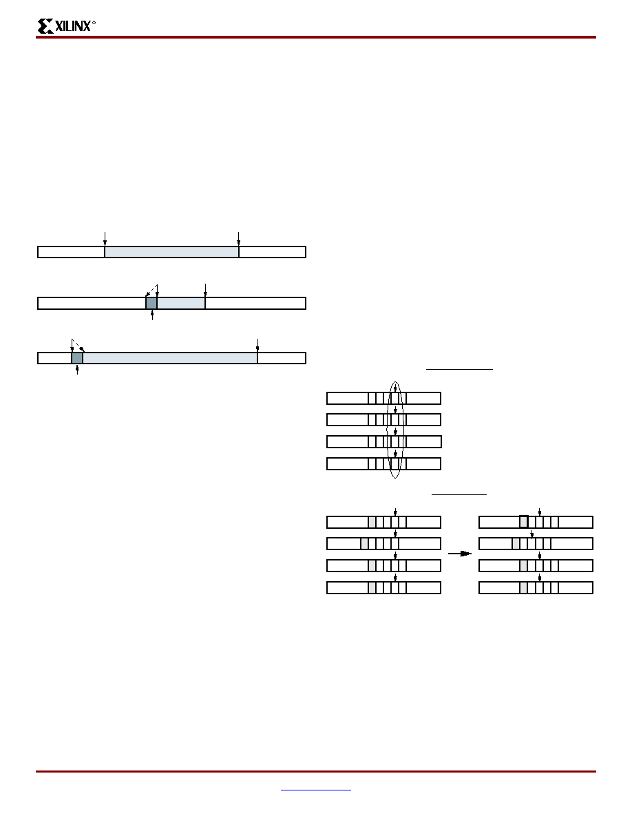
Clock Correction
Clock RXRECCLK (the recovered clock) reflects the data
rate of the incoming data. Clock RXUSRCLK defines the
rate at which the FPGA fabric consumes the data. Ideally,
these rates are identical. However, since the clocks typically
have different sources, one of the clocks will be faster than
the other. The receiver buffer accommodates this difference
between the clock rates. See
Figure 3
.
Nominally, the buffer is always half full. This is shown in the
top buffer,
Figure 3
, where the shaded area represents buff-
ered data not yet read. Received data is inserted via the
write pointer under control of RXRECCLK. The FPGA fabric
reads data via the read pointer under control of RXUSR-
CLK. The half full/half empty condition of the buffer gives a
cushion for the differing clock rates. This operation contin-
ues indefinitely, regardless of whether or not "meaningful"
data is being received. When there is no meaningful data to
be received, the incoming data will consist of IDLE charac-
ters or other padding.
If RXUSRCLK is faster than RXRECCLK, the buffer
becomes more empty over time. The clock correction logic
corrects for this by decrementing the read pointer to reread
a repeatable byte sequence. This is shown in the middle
buffer,
Figure 3
, where the solid read pointer decrements to
the value represented by the dashed pointer. By decrement-
ing the read pointer instead of incrementing it in the usual
fashion, the buffer is partially refilled. The transceiver design
will repeat a single repeatable byte sequence when neces-
sary to refill a buffer. If the byte sequence length is greater
than one, and if attribute CLK_COR_REPEAT_WAIT is 0,
then the transceiver may repeat the same sequence multi-
ple times until the buffer is refilled to the desired extent.
Similarly, if RXUSRCLK is slower than RXRECCLK, the
buffer will fill up over time. The clock correction logic cor-
rects for this by incrementing the read pointer to skip over a
removable byte sequence that need not appear in the final
FPGA fabric byte stream. This is shown in the bottom buffer,
Figure 3
, where the solid read pointer increments to the
value represented by the dashed pointer. This accelerates
the emptying of the buffer, preventing its overflow. The
transceiver design will skip a single byte sequence when
necessary to partially empty a buffer. If attribute
CLK_COR_REPEAT_WAIT is 0, the transceiver may also
skip two consecutive removable byte sequences in one step
to further empty the buffer when necessary.
These operations require the clock correction logic to recog-
nize a byte sequence that can be freely repeated or omitted
in the incoming data stream. This sequence is generally an
IDLE sequence, or other sequence comprised of special
values that occur in the gaps separating packets of mean-
ingful data. These gaps are required to occur sufficiently
often to facilitate the timely execution of clock correction.
Channel Bonding
Some gigabit I/O standards such as Infiniband specify the
use of multiple transceivers in parallel for even higher data
rates. Words of data are split into bytes, with each byte sent
over a separate channel (transceiver). See
Figure 4
.
The top half of the figure shows the transmission of words
split across four transceivers (channels or lanes). PPPP,
QQQQ, RRRR, SSSS, and TTTT represent words sent over
the four channels.
The bottom-left portion of
Figure 4
shows the initial situation
in the FPGA's receivers at the other end of the four chan-
nels. Due to variations in transmission delay--especially if
the channels are routed through repeaters--the FPGA fab-
ric might not correctly assemble the bytes into complete
Figure 3: Clock Correction in Receiver
Read
RXUSRCLK
Read
Read
Write
RXRECCLK
Write
Write
"Nominal" condition: buffer half-full
Buffer less than half -full (emptying)
Buffer more than half-full (filling up)
Repeatable sequence
Removable sequence
DS083-2_15_100901
Figure 4: Channel Bonding (Alignment)
P Q R S T
P Q R S T
P Q R S T
P Q R S T
P Q R S T
P Q R S T
P Q R S T
P Q R S T
P Q R S T
P Q R S T
P Q R S T
P Q R S T
Before channel bonding
After channel bonding
Read
RXUSRCLK
Read
RXUSRCLK
Full word SSSS sent over four channels, one byte per channel
Channel (lane) 0
Channel (lane) 1
Channel (lane) 2
Channel (lane) 3
DS083-2_16_010202
In Transmitters:
In Receivers:
Functional Description: RocketIO Multi-Gigabit Transceiver (MGT)
R
6
www.xilinx.com
DS083-2 (v2.9) October 14, 2003
1-800-255-7778
Advance Product Specification
words. The bottom-left illustration shows the incorrect
assembly of data words PQPP, QRQQ, RSRR, and so forth.
To support correction of this misalignment, the data stream
includes special byte sequences that define corresponding
points in the several channels. In the bottom half of
Figure 4
, the shaded "P" bytes represent these special
characters. Each receiver recognizes the "P" channel bond-
ing character, and remembers its location in the buffer. At
some point, one transceiver designated as the master
instructs all the transceivers to align to the channel bonding
character "P" (or to some location relative to the channel
bonding character).
After this operation, words transmitted to the FPGA fabric
are properly aligned: RRRR, SSSS, TTTT, and so forth, as
shown in the bottom-right portion of
Figure 4
. To ensure that
the channels remain properly aligned following the channel
bonding operation, the master transceiver must also control
the clock correction operations described in the previous
section for all channel-bonded transceivers.
Transmitter Buffer
The transmitter's buffer write pointer (TXUSRCLK) is fre-
quency-locked to its read pointer (REFCLK). Therefore,
clock correction and channel bonding are not required. The
purpose of the transmitter's buffer is to accommodate a
phase difference between TXUSRCLK and REFCLK. A
simple FIFO suffices for this purpose. A FIFO depth of four
will permit reliable operation with simple detection of over-
flow or underflow, which could occur if the clocks are not fre-
quency-locked.
CRC
The RocketIO transceiver CRC logic supports the 32-bit
invariant CRC calculation used by Infiniband, FibreChannel,
and Gigabit Ethernet.
On the transmitter side, the CRC logic recognizes where the
CRC bytes should be inserted and replaces four place-
holder bytes at the tail of a data packet with the computed
CRC. For Gigabit Ethernet and FibreChannel, transmitter
CRC may adjust certain trailing bytes to generate the
required running disparity at the end of the packet.
On the receiver side, the CRC logic verifies the received
CRC value, supporting the same standards as above.
The CRC logic also supports a user mode, with a simple
data packet stucture beginning and ending with
user-defined SOP and EOP characters.
Configuration
This section outlines functions that can be selected or con-
trolled by configuration. Xilinx implementation software sup-
ports 16 transceiver primitives, as shown in
Table 2
.
Each of the primitives in
Table 2
defines default values for
the configuration attributes, allowing some number of them
to be modified by the user. Refer to the RocketIO Trans-
ceiver User Guide for more details.
Reset
The receiver and transmitter have their own synchronous
reset inputs. The transmitter reset recenters the transmis-
sion FIFO, and resets all transmitter registers and the
8B/10B decoder. The receiver reset recenters the receiver
elastic buffer, and resets all receiver registers and the
8B/10B encoder. Neither reset has any effect on the PLLs.
Power
All RocketIO transceivers in the FPGA, whether instantiated
in the design or not, must be connected to power and
ground. Unused transceivers can be powered by any 2.5V
source, and passive filtering is not required.
Power Down
The Power Down module is controlled by the transceiver's
POWERDOWN input pin. The Power Down pin on the
FPGA package has no effect on the transceiver.
Power Sequencing
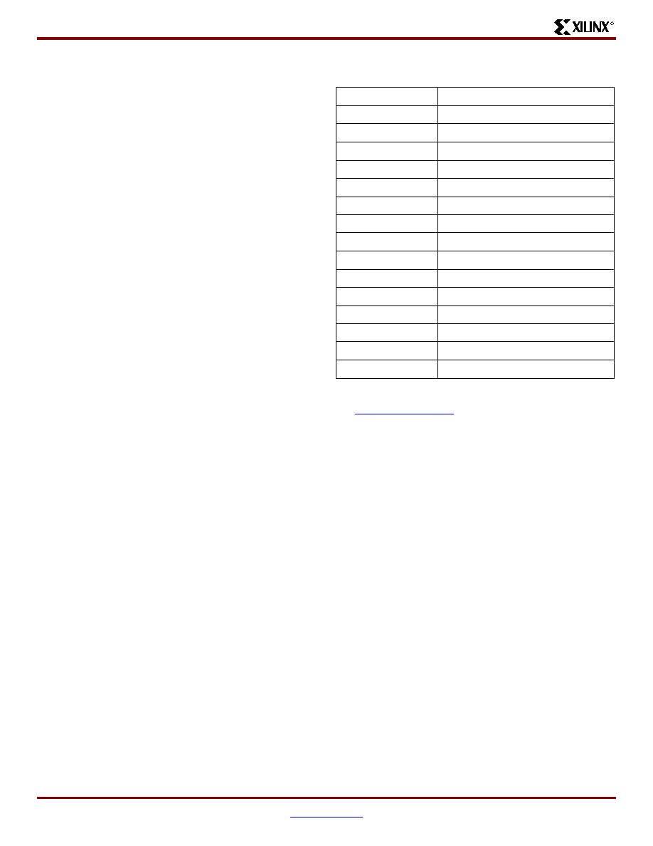
Table 2: Supported RocketIO Transceiver Protocol
Primitives
GT_CUSTOM
Fully customizable by user
GT_FIBRE_CHAN_1
Fibre Channel, 1-byte data path
GT_FIBRE_CHAN_2
Fibre Channel, 2-byte data path
GT_FIBRE_CHAN_4
Fibre Channel, 4-byte data path
GT_ETHERNET_1
Gigabit Ethernet, 1-byte data path
GT_ETHERNET_2
Gigabit Ethernet, 2-byte data path
GT_ETHERNET_4
Gigabit Ethernet, 4-byte data path
GT_XAUI_1
10-gigabit Ethernet, 1-byte data path
GT_XAUI_2
10-gigabit Ethernet, 2-byte data path
GT_XAUI_4
10-gigabit Ethernet, 4-byte data path
GT_INFINIBAND_1
Infiniband, 1-byte data path
GT_INFINIBAND_2
Infiniband, 2-byte data path
GT_INFINIBAND_4
Infiniband, 4-byte data path
GT_AURORA_1
(1)
1-byte data path
GT_AURORA_2
(1)
2-byte data path
GT_AURORA_4
(1)
4-byte data path
Notes:
1.
For more information on the Aurora protocol, visit
http://www.xilinx.com
.

Virtex-II ProTM Platform FPGAs: Functional Description
R
DS083-2 (v2.9) October 14, 2003
www.xilinx.com
7
Advance Product Specification
1-800-255-7778
Functional Description: Processor Block
This section briefly describes the interfaces and compo-
nents of the Processor Block. The subsequent section,
Functional Description: Embedded PowerPC 405 Core
beginning on
page 9
, offers a summary of major PPC405
core features. For an in-depth discussion on both the Pro-
cessor Block and PPC405, see tthe
PowerPC Processor
Reference Guide
and the
PowerPC 405 Processor Block
Reference Guide
available on the Xilinx website at
http://www.xilinx.com
.
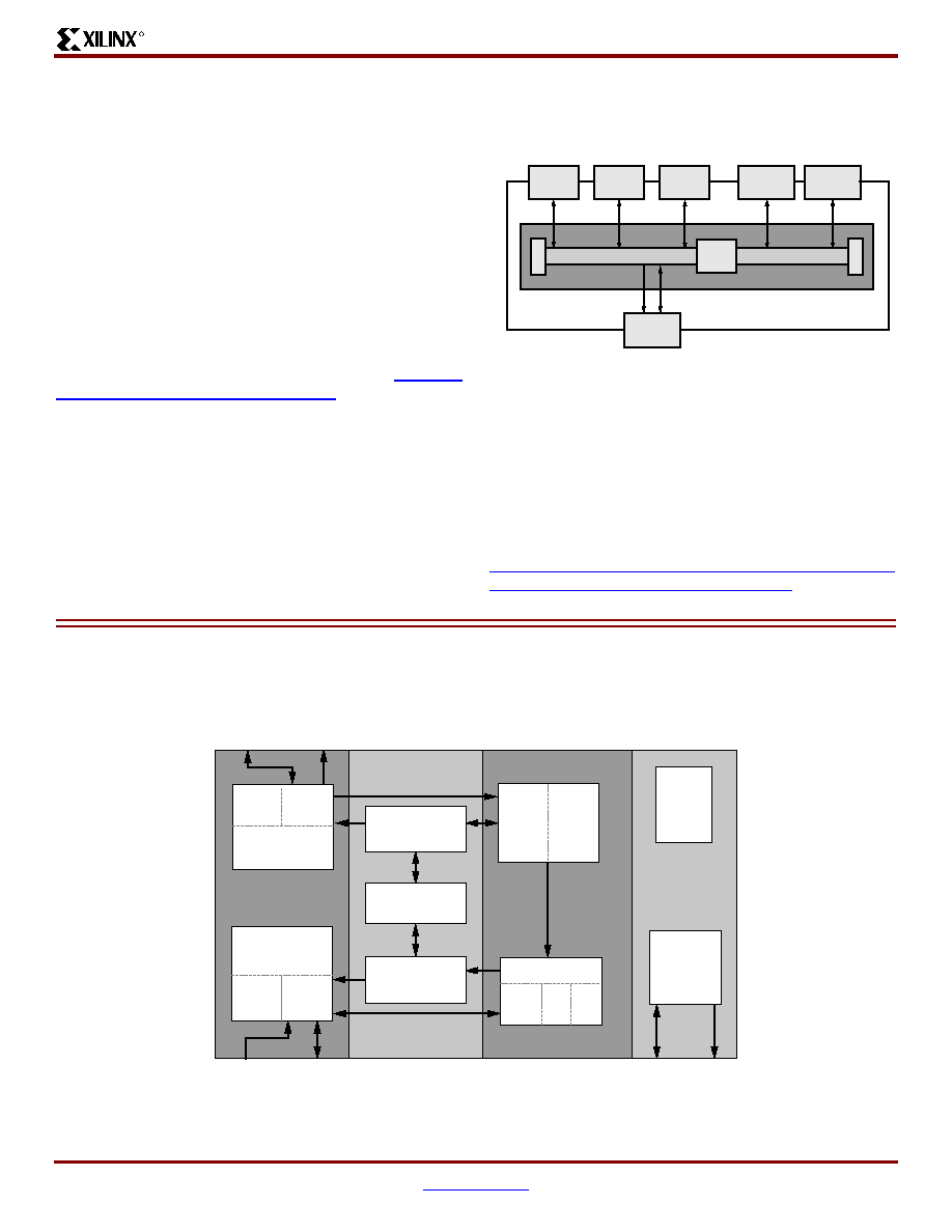
Processor Block Overview
Figure 5
shows the internal architecture of the Processor
Block.
Within the Virtex-II Pro Processor Block, there are four com-
ponents:
∑
Embedded IBM PowerPC 405-D5 RISC CPU core
∑
On-Chip Memory (OCM) controllers and interfaces
∑
Clock/control interface logic
∑
CPU-FPGA Interfaces
Embedded PowerPC 405 RISC Core
The PowerPC 405D5 core is a 0.13 µm implementation of
the IBM PowerPC 405D4 core. The advanced process tech-
nology enables the embedded PowerPC 405 (PPC405)
core to operate at 300+ MHz while maintaining low power
consumption. Specially designed interface logic integrates
the core with the surrounding CLBs, block RAMs, and gen-
eral routing resources. Up to four Processor Blocks can be
available in a single Virtex-II Pro device.
The embedded PPC405 core implements the PowerPC
User Instruction Set Architecture (UISA), user-level regis-
ters, programming model, data types, and addressing
modes for 32-bit fixed-point operations. 64-bit operations,
auxiliary processor operations, and floating-point opera-
tions are trapped and can be emulated in software.
Most of the PPC405 core features are compatible with the
specifications for the PowerPC Virtual Environment
Architecture (VEA) and Operating Environment Architecture
(OEA). They also provide a number of optimizations and
extensions to the lower layers of the PowerPC Architecture.
The full architecture of the PPC405 is defined by the
PowerPC Embedded Environment and PowerPC UISA
documentation, available from IBM.
On-Chip Memory (OCM) Controllers
Introduction
The OCM controllers serve as dedicated interfaces
between the block RAMs in the FPGA fabric (see
18 Kb
Block SelectRAM+ Resources, page 33
) and OCM signals
available on the embedded PPC405 core. The OCM signals
on the PPC405 core are designed to provide very quick
access to a fixed amount of instruction and data memory
space. The OCM controller provides an interface to both the
64-bit Instruction-Side Block RAM (ISBRAM) and the 32-bit
Data-Side Block RAM (DSBRAM). The designer can
choose to implement:
∑
ISBRAM only
∑
DSBRAM only
∑
Both ISBRAM and DSBRAM
∑
No ISBRAM and no DSBRAM
One of OCM's primary advantages is that it guarantees a
fixed latency of execution for a higher level of determinism.
Additionally, it reduces cache pollution and thrashing, since
the cache remains available for caching code from other
memory resources.
Typical applications for DSOCM include scratch-pad mem-
ory, as well as use of the dual-port feature of block RAM to
enable bidirectional data transfer between processor and
FPGA. Typical applications for ISOCM include storage of
interrupt service routines.
Functional Features
Common Features
∑
Separate Instruction and Data memory interface
between processor core and BRAMs in FPGA
∑
Dedicated interface to Device Control Register (DCR)
bus for ISOCM and DSOCM
Figure 5: Processor Block Architecture
Processor Block = CPU Core + Interface Logic + CPU-FPGA Interface
DS083-2_03a_060701
PPC 405
Core
OCM
Controller
OCM
Controller
Control
BRAM
BRAM
BRAM
BRAM
FPGA CLB Array
Interface Logic
CPU-FPGA Interfaces

Functional Description: Processor Block
R
8
www.xilinx.com
DS083-2 (v2.9) October 14, 2003
1-800-255-7778
Advance Product Specification
∑
Single-cycle and multi-cycle mode option for I-side and
D-side interfaces
∑
Single cycle = one CPU clock cycle;
multi-cycle = minimum of two and maximum of eight
CPU clock cycles
∑
FPGA configurable DCR addresses within DSOCM
and ISOCM.
∑
Independent 16 MB logical memory space available
within PPC405 memory map for each of the DSOCM
and ISOCM. The number of block RAMs in the device
might limit the maximum amount of OCM supported.
∑
Maximum of 64K and 128K bytes addressable from
DSOCM and ISOCM interfaces, respectively, using
address outputs from OCM directly without additional
decoding logic.
Data-Side OCM (DSOCM)
∑
32-bit Data Read bus and 32-bit Data Write bus
∑
Byte write access to DSBRAM support
∑
Second port of dual port DSBRAM is available to
read/write from an FPGA interface
∑
22-bit address to DSBRAM port
∑
8-bit DCR Registers: DSCNTL, DSARC
∑
Three alternatives to write into DSBRAM: BRAM
initialization, CPU, FPGA H/W using second port
Instruction-Side OCM (ISOCM)
The ISOCM interface contains a 64-bit read only port, for
instruction fetches, and a 32-bit write only port, to initialize
or test the ISBRAM. When implementing the read only port,
the user must deassert the write port inputs. The preferred
method of initializing the ISBRAM is through the configura-
tion bitstream.
∑
64-bit Data Read Only bus (two instructions per cycle)
∑
32-bit Data Write Only bus (through DCR)
∑
Separate 21-bit address to ISBRAM
∑
8-bit DCR Registers: ISCNTL, ISARC
∑
32-bit DCR Registers: ISINIT, ISFILL
∑
Two alternatives to write into ISBRAM: BRAM
initialization, DCR and write instruction
Clock/Control Interface Logic
The clock/control interface logic provides proper initializa-
tion and connections for PPC405 clock/power manage-
ment, resets, PLB cycle control, and OCM interfaces. It also
couples user signals between the FPGA fabric and the
embedded PPC405 CPU core.
The processor clock connectivity is similar to CLB clock
pins. It can connect either to global clock nets or general
routing resources. Therefore the processor clock source
can come from DCM, CLB, or user package pin.
CPU-FPGA Interfaces
All Processor Block user pins link up with the general FPGA
routing resources through the CPU-FPGA interface. There-
fore processor signals have the same routability as other
non-Processor Block user signals. Longlines and hex lines
travel across the Processor Block both vertically and hori-
zontally, allowing signals to route through the Processor
Block.
Processor Local Bus (PLB) Interfaces
The PPC405 core accesses high-speed system resources
through PLB interfaces on the instruction and data cache
controllers. The PLB interfaces provide separate 32-bit
address/64-bit data buses for the instruction and data sides.
The cache controllers are both PLB masters. PLB arbiters
are implemented in the FPGA fabric and are available as
soft IP cores.
Device Control Register (DCR) Bus Interface
The device control register (DCR) bus has 10 bits of
address space for components external to the PPC405
core. Using the DCR bus to manage status and configura-
tion registers reduces PLB traffic and improves system
integrity. System resources on the DCR bus are protected
or isolated from wayward code since the DCR bus is not
part of the system memory map.
External Interrupt Controller (EIC) Interface
Two level-sensitive user interrupt pins (critical and non-criti-
cal) are available. They can be either driven by user defined
logic or Xilinx soft interrupt controller IP core outside the
Processor Block.
Clock/Power Management (CPM) Interface
The CPM interface supports several methods of clock distri-
bution and power management. Three modes of operation
that reduce power consumption below the normal opera-
tional level are available.
Reset Interface
There are three user reset input pins (core, chip, and sys-
tem) and three user reset output pins for different levels of
reset, if required.
Debug Interface
Debugging interfaces on the embedded PPC405 core, con-
sisting of the JTAG and Trace ports, offer access to
resources internal to the core and assist in software devel-
opment. The JTAG port provides basic JTAG chip testing
functionality as well as the ability for external debug tools to
gain control of the processor for debug purposes. The Trace
port furnishes programmers with a mechanism for acquiring
instruction execution traces.
The JTAG port complies with IEEE Std 1149.1, which
defines a test access port (TAP) and boundary scan
architecture. Extensions to the JTAG interface provide
Virtex-II ProTM Platform FPGAs: Functional Description
R
DS083-2 (v2.9) October 14, 2003
www.xilinx.com
9
Advance Product Specification
1-800-255-7778
debuggers with processor control that includes stopping,
starting, and stepping the PPC405 core. These extensions
are compliant with the IEEE 1149.1 specifications for
vendor-specific extensions.
The Trace port provides instruction execution trace informa-
tion to an external trace tool. The PPC405 core is capable of
back trace and forward trace. Back trace is the tracing of
instructions prior to a debug event while forward trace is the
tracing of instructions after a debug event.
The processor JTAG port and the FPGA JTAG port can be
accessed independently, or the two can be programmati-
cally linked together and accessed via the dedicated FPGA
JTAG pins.
For detailed information on the PPC405 JTAG interface,
please refer to the "JTAG Interface" section of the
PowerPC
405 Processor Block Reference Guide
CoreConnectTM Bus Architecture
The Processor Block is compatible with the CoreConnectTM
bus architecture. Any CoreConnect compliant cores includ-
ing Xilinx soft IP can integrate with the Processor Block
through this high-performance bus architecture imple-
mented on FPGA fabric.
The CoreConnect architecture provides three buses for
interconnecting Processor Blocks, Xilinx soft IP, third party
IP, and custom logic, as shown in
Figure 6
:
∑
Processor Local Bus (PLB)
∑
On-Chip Peripheral Bus (OPB)
∑
Device Control Register (DCR) bus
High-performance peripherals connect to the high-band-
width, low-latency PLB. Slower peripheral cores connect to
the OPB, which reduces traffic on the PLB, resulting in
greater overall system performance.
For more information, refer to:
http://www-3.ibm.com/chips/techlib/techlib.nfs/product
families/CoreConnect_Bus_Architecture/
Functional Description: Embedded PowerPC 405 Core
This section offers a brief overview of the various functional blocks shown in
Figure 7
.
Figure 6: CoreConnect Block Diagram
DS083-2_02a_010202
System
Core
System
Core
System
Core
Processor
Block
Peripheral
Core
Peripheral
Core
Processor Local Bus
On-Chip Peripheral Bus
Bus
Bridge
CoreConnect Bus Architecture
Arbiter
Arbiter
DCR Bus
Instruction
Data
DCR Bus
DCR
Bus
Figure 7: Embedded PPC405 Core Block Diagram
MAC
ALU
DS083-2_01_062001
PLB Master
Interface
Data
OCM
JTAG
Instruction
Trace
D-Cache
Controller
D-Cache
Array
I-Cache
Controller
I-Cache
Array
Data
Cache
Unit
Instruction
Cache
Unit
32 x 32
GPR
Execution Unit (EXU)
PLB Master
Interface
Instruction
OCM
Instruction Shadow
TLB
(4 Entry)
Unified TLB
(64 Entry)
Data Shadow
TLB
(8 Entry)
Fetch
and
Decode
Logic
3-Element
Fetch
Queue
(PFB1,
PFB0,
DCD)
Timers
(FIT,
PIT,
Watchdog)
Debug Logic
Timers
&
Debug
Fetch & Decode
MMU
Cache Units
Execution Unit

Functional Description: Embedded PowerPC 405 Core
R
10
www.xilinx.com
DS083-2 (v2.9) October 14, 2003
1-800-255-7778
Advance Product Specification
Embedded PPC405 Core
The embedded PPC405 core is a 32-bit Harvard architec-
ture processor.
Figure 7
illustrates its functional blocks:
∑
Cache units
∑
Memory Management unit
∑
Fetch Decode unit
∑
Execution unit
∑
Timers
∑
Debug logic unit
It operates on instructions in a five stage pipeline consisting
of a fetch, decode, execute, write-back, and load write-back
stage. Most instructions execute in a single cycle, including
loads and stores.
Instruction and Data Cache
The embedded PPC405 core provides an instruction cache
unit (ICU) and a data cache unit (DCU) that allow concur-
rent accesses and minimize pipeline stalls. The instruction
and data cache array are 16 KB each. Both cache units are
two-way set associative. Each way is organized into 256
lines of 32 bytes (eight words). The instruction set provides
a rich assortment of cache control instructions, including
instructions to read tag information and data arrays.
The PPC405 core accesses external memory through the
instruction (ICU) and data cache units (DCU). The cache
units each include a 64-bit PLB master interface, cache
arrays, and a cache controller. The ICU and DCU handle
cache misses as requests over the PLB to another PLB
device such as an external bus interface unit. Cache hits are
handled as single cycle memory accesses to the instruction
and data caches.
Instruction Cache Unit (ICU)
The ICU provides one or two instructions per cycle to the
instruction queue over a 64-bit bus. A line buffer (built into
the output of the array for manufacturing test) enables the
ICU to be accessed only once for every four instructions, to
reduce power consumption by the array.
The ICU can forward any or all of the four or eight words of
a line fill to the EXU to minimize pipeline stalls caused by
cache misses. The ICU aborts speculative fetches aban-
doned by the EXU, eliminating unnecessary line fills and
enabling the ICU to handle the next EXU fetch. Aborting
abandoned requests also eliminates unnecessary external
bus activity, thereby increasing external bus utilization.
Data Cache Unit (DCU)
The DCU transfers one, two, three, four, or eight bytes per
cycle, depending on the number of byte enables presented
by the CPU. The DCU contains a single-element command
and store data queue to reduce pipeline stalls; this queue
enables the DCU to independently process load/store and
cache control instructions. Dynamic PLB request prioritiza-
tion reduces pipeline stalls even further. When the DCU is
busy with a low-priority request while a subsequent storage
operation requested by the CPU is stalled; the DCU auto-
matically increases the priority of the current request to the
PLB.
The DCU provides additional features that allow the pro-
grammer to tailor its performance for a given application.
The DCU can function in write-back or write-through mode,
as controlled by the Data Cache Write-through Register
(DCWR) or the Translation Look-aside Buffer (TLB); the
cache controller can be tuned for a balance of performance
and memory coherency. Write-on-allocate, controlled by the
store word on allocate (SWOA) field of the Core Configura-
tion Register 0 (CCR0), can inhibit line fills caused by store
misses, to further reduce potential pipeline stalls and
unwanted external bus traffic.
Fetch and Decode Logic
The fetch/decode logic maintains a steady flow of instruc-
tions to the execution unit by placing up to two instructions
in the fetch queue. The fetch queue consists of three buff-
ers: pre-fetch buffer 1 (PFB1), pre-fetch buffer 0 (PFB0),
and decode (DCD). The fetch logic ensures that instructions
proceed directly to decode when the queue is empty.
Static branch prediction as implemented on the PPC405
core takes advantage of some standard statistical proper-
ties of code. Branches with negative address displacement
are by default assumed taken. Branches that do not test the
condition or count registers are also predicted as taken. The
PPC405 core bases branch prediction upon these default
conditions when a branch is not resolved and speculatively
fetches along the predicted path. The default prediction can
be overridden by software at assembly or compile time.
Branches are examined in the decode and pre-fetch buffer 0
fetch queue stages. Two branch instructions can be handled
simultaneously. If the branch in decode is not taken, the
fetch logic fetches along the predicted path of the branch
instruction in pre-fetch buffer 0. If the branch in decode is
taken, the fetch logic ignores the branch instruction in
pre-fetch buffer 0.
Execution Unit
The embedded PPC405 core has a single issue execution
unit (EXU) containing the register file, arithmetic logic unit
(ALU), and the multiply-accumulate (MAC) unit. The execu-
tion unit performs all 32-bit PowerPC integer instructions in
hardware.
The register file is comprised of thirty-two 32-bit general
purpose registers (GPR), which are accessed with three
read ports and two write ports. During the decode stage,
data is read out of the GPRs and fed to the execution unit.
Likewise, during the write-back stage, results are written to
the GPR. The use of the five ports on the register file
enables either a load or a store operation to execute in par-
allel with an ALU operation.

Virtex-II ProTM Platform FPGAs: Functional Description
R
DS083-2 (v2.9) October 14, 2003
www.xilinx.com
11
Advance Product Specification
1-800-255-7778
Memory Management Unit (MMU)
The embedded PPC405 core has a 4 GB address space,
which is presented as a flat address space.
The MMU provides address translation, protection func-
tions, and storage attribute control for embedded applica-
tions. The MMU supports demand-paged virtual memory
and other management schemes that require precise con-
trol of logical-to-physical address mapping and flexible
memory protection. Working with appropriate system-level
software, the MMU provides the following functions:
∑
Translation of the 4 GB effective address space into
physical addresses
∑
Independent enabling of instruction and data
translation/protection
∑
Page-level access control using the translation
mechanism
∑
Software control of page replacement strategy
∑
Additional control over protection using zones
∑
Storage attributes for cache policy and speculative
memory access control
The MMU can be disabled under software control. If the
MMU is not used, the PPC405 core provides other storage
control mechanisms.
Translation Look-Aside Buffer (TLB)
The Translation Look-Aside Buffer (TLB) is the hardware
resource that controls translation and protection. It consists
of 64 entries, each specifying a page to be translated. The
TLB is fully associative; a given page entry can be placed
anywhere in the TLB. The translation function of the MMU
occurs pre-cache. Cache tags and indexing use physical
addresses.
Software manages the establishment and replacement of
TLB entries. This gives system software significant flexibility
in implementing a custom page replacement strategy. For
example, to reduce TLB thrashing or translation delays,
software can reserve several TLB entries in the TLB for glo-
bally accessible static mappings. The instruction set pro-
vides several instructions used to manage TLB entries.
These instructions are privileged and require the software
to be executing in supervisor state. Additional TLB instruc-
tions are provided to move TLB entry fields to and from
GPRs.
The MMU divides logical storage into pages. Eight page
sizes (1 KB, 4 KB, 16 KB, 64 KB, 256 KB, 1 MB, 4 MB, and
16 MB) are simultaneously supported, such that, at any
given time, the TLB can contain entries for any combination
of page sizes. In order for a logical to physical translation to
exist, a valid entry for the page containing the logical
address must be in the TLB. Addresses for which no TLB
entry exists cause TLB-Miss exceptions.
To improve performance, four instruction-side and eight
data-side TLB entries are kept in shadow arrays. The
shadow arrays allow single-cycle address translation and
also help to avoid TLB contention between load/store and
instruction fetch operations. Hardware manages the
replacement and invalidation of shadow-TLB entries; no
system software action is required.
Memory Protection
When address translation is enabled, the translation mech-
anism provides a basic level of protection.
The Zone Protection Register (ZPR) enables the system
software to override the TLB access controls. For example,
the ZPR provides a way to deny read access to application
programs. The ZPR can be used to classify storage by type;
access by type can be changed without manipulating indi-
vidual TLB entries.
The PowerPC Architecture provides WIU0GE (write-back /
write-through, cacheability, user-defined 0, guarded,
endian) storage attributes that control memory accesses,
using bits in the TLB or, when address translation is dis-
abled, storage attribute control registers.
When address translation is enabled, storage attribute con-
trol bits in the TLB control the storage attributes associated
with the current page. When address translation is disabled,
bits in each storage attribute control register control the
storage attributes associated with storage regions. Each
storage attribute control register contains 32 fields. Each
field sets the associated storage attribute for a 128 MB
memory region.
Timers
The embedded PPC405 core contains a 64-bit time base
and three timers, as shown in
Figure 8
:
∑
Programmable Interval Timer (PIT)
∑
Fixed Interval Timer (FIT)
∑
Watchdog Timer (WDT)
The time base counter increments either by an internal sig-
nal equal to the CPU clock rate or by a separate external
timer clock signal. No interrupts are generated when the
time base rolls over. The three timers are synchronous with
the time base.
The PIT is a 32-bit register that decrements at the same rate
as the time base is incremented. The user loads the PIT
register with a value to create the desired delay. When the
register reaches zero, the timer stops decrementing and
generates a PIT interrupt. Optionally, the PIT can be pro-
grammed to auto-reload the last value written to the PIT
register, after which the PIT continues to decrement.
The FIT generates periodic interrupts based on one of four
selectable bits in the time base. When the selected bit
changes from 0 to 1, the PPC405 core generates a FIT
interrupt.
The WDT provides a periodic critical-class interrupt based
on a selected bit in the time base. This interrupt can be used
for system error recovery in the event of software or system
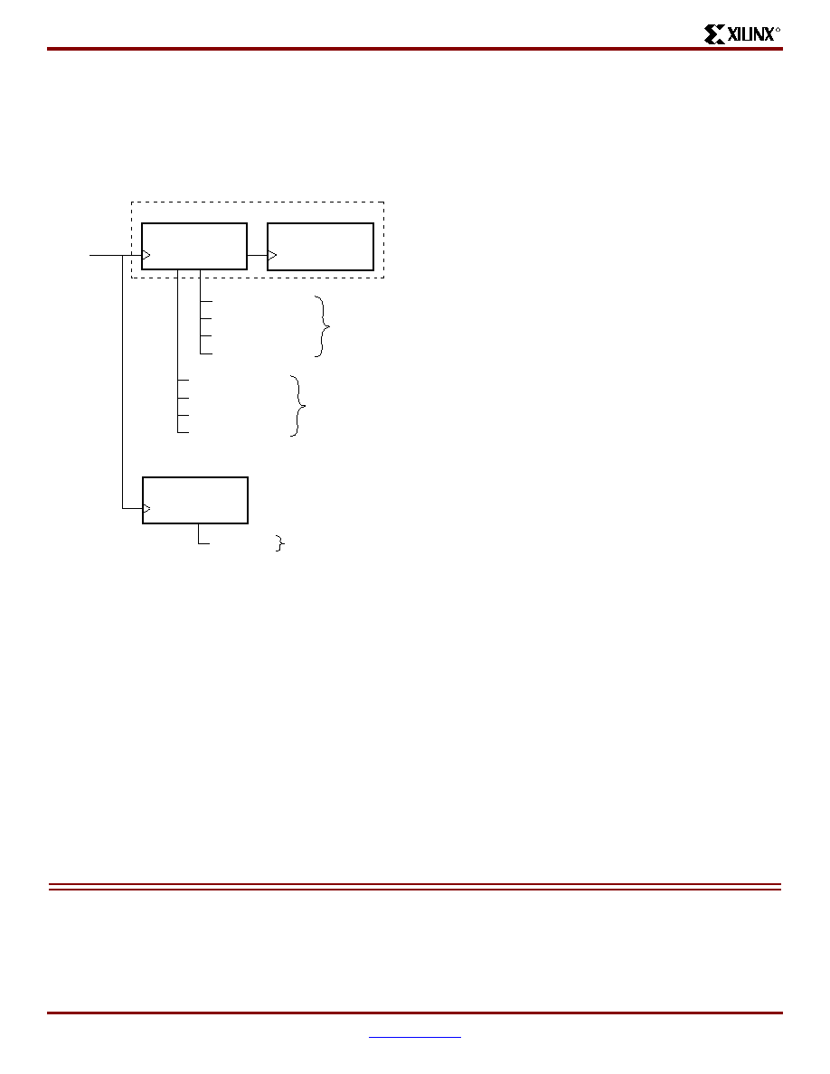
Functional Description: Embedded PowerPC 405 Core
R
12
www.xilinx.com
DS083-2 (v2.9) October 14, 2003
1-800-255-7778
Advance Product Specification
lockups. Users may select one of four time periods for the
interval and the type of reset generated if the WDT expires
twice without an intervening clear from software. If enabled,
the watchdog timer generates a reset unless an exception
handler updates the WDT status bit before the timer has
completed two of the selected timer intervals.
Interrupts
The PPC405 provides an interface to an interrupt controller
that is logically outside the PPC405 core. This controller
combines the asynchronous interrupt inputs and presents
them to the embedded core as a single interrupt signal. The
sources of asynchronous interrupts are external signals, the
JTAG/debug unit, and any implemented peripherals.
Debug Logic
All architected resources on the embedded PPC405 core
can be accessed through the debug logic. Upon a debug
event, the PPC405 core provides debug information to an
external debug tool. Three different types of tools are sup-
ported depending on the debug mode: ROM monitors,
JTAG debuggers, and instruction trace tools.
In internal debug mode, a debug event enables excep-
tion-handling software at a dedicated interrupt vector to take
over the CPU core and communicate with a debug tool. The
debug tool has read-write access to all registers and can set
hardware or software breakpoints. ROM monitors typically
use the internal debug mode.
In external debug mode, the CPU core enters stop state
(stops instruction execution) when a debug event occurs.
This mode offers a debug tool read-write access to all regis-
ters in the PPC405 core. Once the CPU core is in stop state,
the debug tool can start the CPU core, step an instruction,
freeze the timers, or set hardware or software break points.
In addition to CPU core control, the debug logic is capable
of writing instructions into the instruction cache, eliminating
the need for external memory during initial board bring-up.
Communication to a debug tool using external debug mode
is through the JTAG port.
Debug wait mode offers the same functionality as external
debug mode with one exception. In debug wait mode, the
CPU core goes into wait state instead of stop state after a
debug event. Wait state is identical to stop state until an
interrupt occurs. In wait state, the PPC405 core can vector
to an exception handler, service an interrupt and return to
wait state. This mode is particularly useful when debugging
real time control systems.
Real-time trace debug mode is always enabled. The debug
logic continuously broadcasts instruction trace information
to the trace port. When a debug event occurs, the debug
logic signals an external debug tool to save instruction trace
information before and after the event. The number of
instructions traced depends on the trace tool.
Debug events signal the debug logic to stop the CPU core,
put the CPU core in debug wait state, cause a debug excep-
tion or save instruction trace information.
Big Endian and Little Endian Support
The embedded PPC405 core supports big endian or little
endian byte ordering for instructions stored in external
memory. Since the PowerPC architecture is big endian
internally, the ICU rearranges the instructions stored as little
endian into the big endian format. Therefore, the instruction
cache always contains instructions in big endian format so
that the byte ordering is correct for the execution unit. This
feature allows the 405 core to be used in systems designed
to function in a little endian environment.
Figure 8: Relationship of Timer Facilities to Base Clock
TBU (32 bits)
Bit 3 (2
29
clocks)
Bit 7 (2
25
clocks)
Bit 11 (2
21
clocks)
Bit 15 (2
17
clocks)
Bit 11
(2
21
clocks)
Bit 15
(2
17
clocks)
Bit 19
(2
13
9
clocks)
Bit 23
(2 clocks)
WDT Events
FIT Events
Time Base (Incrementer)
31
TBL (32 bits)
31
0
0
PIT (Decrementer)
(32 bits)
31
0
Zero Detect
PIT Events
External
Clock
Source
DS083-2_06_062001
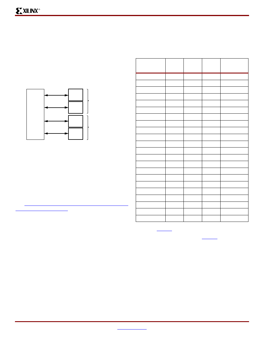
Virtex-II ProTM Platform FPGAs: Functional Description
R
DS083-2 (v2.9) October 14, 2003
www.xilinx.com
13
Advance Product Specification
1-800-255-7778
Functional Description: FPGA
Input/Output Blocks (IOBs)
Virtex-II Pro I/O blocks (IOBs) are provided in groups of two
or four on the perimeter of each device. Each IOB can be
used as input and/or output for single-ended I/Os. Two IOBs
can be used as a differential pair. A differential pair is always
connected to the same switch matrix, as shown in
Figure 9
.
IOB blocks are designed for high-performance I/O, support-
ing 22 single-ended standards, as well as differential sig-
naling with LVDS, LDT, bus LVDS, and LVPECL.
Note: Differential I/Os must use the same clock.
Supported I/O Standards
Virtex-II Pro IOB blocks feature SelectIO-Ultra inputs and out-
puts that support a wide variety of I/O signaling standards. In
addition to the internal supply voltage (V
CCINT
= 1.5V), out-
put driver supply voltage (V
CCO
) is dependent on the I/O stan-
dard (see
Table 3
and
Table 4
). An auxiliary supply voltage
(V
CCAUX
= 2.5V) is required, regardless of the I/O standard
used. For exact supply voltage absolute maximum ratings,
see
Virtex-II ProTM Platform FPGAs: DC and Switching
Characteristics (Module 3)
.
All of the user IOBs have fixed-clamp diodes to V
CCO
and to
ground. The IOBs are not compatible or compliant with 5V
I/O standards (not 5V-tolerant).
Table 5
lists supported I/O standards with Digitally Con-
trolled Impedance. See
Digitally Controlled Impedance
(DCI), page 19
.
Figure 9: Virtex-II Pro Input/Output Tile
IOB
PAD4
IOB
PAD3
Differential Pair
IOB
PAD2
IOB
PAD1
Differential Pair
Switch
Matrix
DS083-2_30_010202
Table 3: Supported Single-Ended I/O Standards
I/O
Standard
Output
V
CCO
Input
V
CCO
Input
V
REF
Board
Termination
Voltage (V
TT
)
LVTTL
(1)
3.3
3.3
N/R
N/R
LVCMOS33
(1)
3.3
3.3
N/R
N/R
LVCMOS25
2.5
2.5
N/R
N/R
LVCMOS18
1.8
1.8
N/R
N/R
LVCMOS15
1.5
1.5
N/R
N/R
PCI33_3
Note (2)
Note (2)
N/R
N/R
PCI66_3
Note (2)
Note (2)
N/R
N/R
PCI-X
Note (2)
Note (2)
N/R
N/R
GTL
Note (3)
Note (3)
0.8
1.2
GTLP
Note (3)
Note (3)
1.0
1.5
HSTL_I
1.5
N/R
0.75
0.75
HSTL_II
1.5
N/R
0.75
0.75
HSTL_III 1.5
N/R
0.9
1.5
HSTL_IV
1.5
N/R
0.9
1.5
HSTL_I_18
1.8 N/R
0.9
0.9
HSTL_II_18
1.8
N/R
0.9
0.9
HSTL_III _18
1.8
N/R
1.1
1.8
HSTL_IV_18
1.8
N/R
1.1
1.8
SSTL2_I 2.5
N/R
1.25
1.25
SSTL2_II
2.5
N/R
1.25
1.25
SSTL18_I
(4)
1.8
N/R
0.9
0.9
SSTL18_II
1.8
N/R
0.9
0.9
Notes:
1.
Refer to
XAPP659
for more details on interfacing to these 3.3V
standards.
2.
For PCI and PCI-X standards, refer to
XAPP653
.
3.
V
CCO
of GTL or GTLP should not be lower than the termination
voltage or the voltage seen at the I/O pad.
4.
SSTL18_I is not a JEDEC-supported standard.
5.
N/R = no requirement.
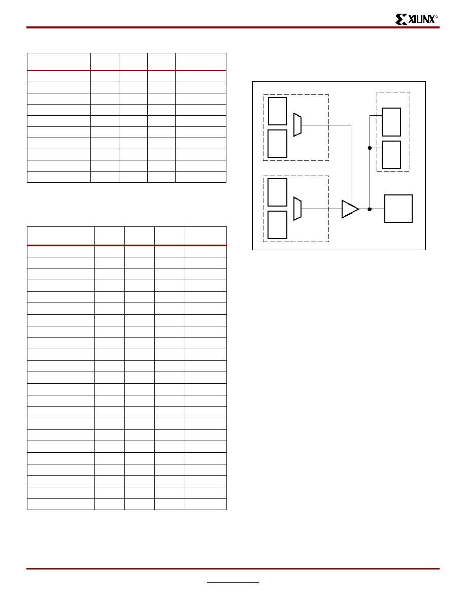
Functional Description: FPGA
R
14
www.xilinx.com
DS083-2 (v2.9) October 14, 2003
1-800-255-7778
Advance Product Specification
Logic Resources
IOB blocks include six storage elements, as shown in
Figure 10
.
Each storage element can be configured either as an
edge-triggered D-type flip-flop or as a level-sensitive latch.
On the input, output, and 3-state path, one or two DDR reg-
isters can be used.
Double data rate is directly accomplished by the two regis-
ters on each path, clocked by the rising edges (or falling
edges) from two different clock nets. The two clock signals
are generated by the DCM and must be 180 degrees out of
phase, as shown in
Figure 11
. There are two input, output,
and 3-state data signals, each being alternately clocked out.
Table 4: Supported Differential Signal I/O Standards
I/O
Standard
Output
V
CCO
Input
V
CCO
Input
V
REF
Output
V
OD
LDT_25
2.5
N/R
N/R
0.500 ≠ 0.740
LVDS_25
2.5
N/R
N/R
0.247 ≠ 0.454
LVDSEXT_25
2.5
N/R
N/R
0.330 ≠ 0.700
BLVDS_25
2.5
N/R
N/R
0.250 ≠ 0.450
ULVDS_25
2.5
N/R
N/R
0.500 ≠ 0.740
LVPECL_25
2.5
N/R
N/R
0.345 ≠ 1.185
LDT_25_DT
(1)
2.5
2.5
N/R
0.500 ≠ 0.740
LVDS_25_DT
(1)
2.5
2.5
N/R
0.247 ≠ 0.454
LVDSEXT_25_DT
(1)
2.5
2.5
N/R
0.330 ≠ 0.700
ULVDS_25_DT
(1)
2.5
2.5
N/R
0.500 ≠ 0.740
Notes:
1.
These standards support on-chip 100
termination.
2.
N/R = no requirement.
Table 5: Supported DCI I/O Standards
I/O
Standard
Output
V
CCO
Input
V
CCO
Input
V
REF
Termination
Type
LVDCI_33
(1)
3.3
3.3
N/R
Series
LVDCI_25
2.5
2.5
N/R
Series
LVDCI_DV2_25
2.5
2.5
N/R
Series
LVDCI_18
1.8
1.8
N/R
Series
LVDCI_DV2_18
1.8
1.8
N/R
Series
LVDCI_15
1.5
1.5
N/R
Series
LVDCI_DV2_15
1.5
1.5
N/R
Series
GTL_DCI
1.2
1.2
0.8
Single
GTLP_DCI
1.5
1.5
1.0
Single
HSTL_I_DCI
1.5
1.5
0.75
Split
HSTL_II_DCI
1.5
1.5
0.75
Split
HSTL_III_DCI
1.5
1.5
0.9
Single
HSTL_IV_DCI
1.5
1.5
0.9
Single
HSTL_I_DCI_18
1.8
1.8
0.9
Split
HSTL_II_DCI_18
1.8
1.8
0.9
Split
HSTL_III_DCI_18
1.8
1.8
1.1
Single
HSTL_IV_DCI_18
1.8
1.8
1.1
Single
SSTL2_I_DCI
(2)
2.5
2.5
1.25
Split
SSTL2_II_DCI
(2)
2.5
2.5
1.25
Split
SSTL18_I_DCI
(3)
1.8
1.8
0.9
Split
SSTL18_II_DCI
1.8
1.8
0.9
Split
LVDS_25_DCI
2.5
2.5
N/R
Split
LVDSEXT_25_DCI
2.5
2.5
N/R
Split
Notes:
1.
LVDCI_XX is LVCMOS output controlled impedance buffers,
matching all or half of the reference resistors.
2.
These are SSTL compatible.
3.
SSTL18_I is not a JEDEC-supported standard.
4.
N/R = no requirement.
Figure 10: Virtex-II Pro IOB Block
Reg
OCK1
Reg
OCK2
Reg
ICK1
Reg
ICK2
DDR mux
Input
PAD
3-State
Reg
OCK1
Reg
OCK2
DDR mux
Output
IOB
DS031_29_100900
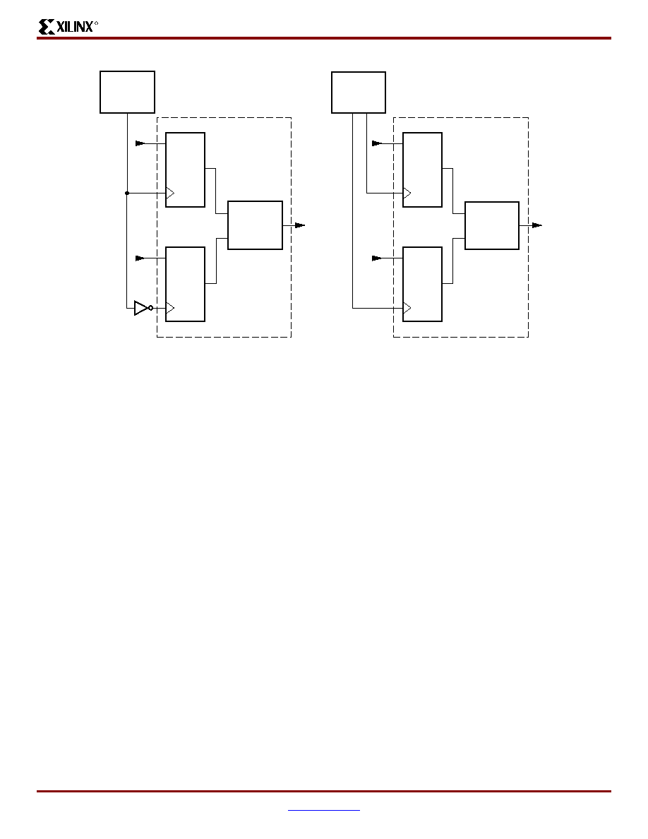
Virtex-II ProTM Platform FPGAs: Functional Description
R
DS083-2 (v2.9) October 14, 2003
www.xilinx.com
15
Advance Product Specification
1-800-255-7778
This DDR mechanism can be used to mirror a copy of the
clock on the output. This is useful for propagating a clock
along the data that has an identical delay. It is also useful for
multiple clock generation, where there is a unique clock
driver for every clock load. Virtex-II Pro devices can pro-
duce many copies of a clock with very little skew.
Each group of two registers has a clock enable signal (ICE
for the input registers, OCE for the output registers, and
TCE for the 3-state registers). The clock enable signals are
active High by default. If left unconnected, the clock enable
for that storage element defaults to the active state.
Each IOB block has common synchronous or asynchronous
set and reset (SR and REV signals). Two neighboring IOBs
have a shared routing resource connecting the ICLK and
OTCLK pins on pairs of IOBs. If two adjacent IOBs using
DDR registers do not share the same clock signals on their
clock pins (ICLK1, ICLK2, OTCLK1, and OTCLK2), one of
the clock signals will be unroutable.
The IOB pairing is identical to the LVDS IOB pairs. Hence,
the package pin-out table can also be used for pin assign-
ment to avoid conflict.
SR forces the storage element into the state specified by the
SRHIGH or SRLOW attribute. SRHIGH forces a logic 1.
SRLOW forces a logic "0". When SR is used, a second input
(REV) forces the storage element into the opposite state. The
reset condition predominates over the set condition. The ini-
tial state after configuration or global initialization state is
defined by a separate INIT0 and INIT1 attribute. By default,
the SRLOW attribute forces INIT0, and the SRHIGH attribute
forces INIT1.
For each storage element, the SRHIGH, SRLOW, INIT0,
and INIT1 attributes are independent. Synchronous or
asynchronous set / reset is consistent in an IOB block.
All the control signals have independent polarity. Any
inverter placed on a control input is automatically absorbed.
Each register or latch, independent of all other registers or
latches, can be configured as follows:
∑
No set or reset
∑
Synchronous set
∑
Synchronous reset
∑
Synchronous set and reset
∑
Asynchronous set (preset)
∑
Asynchronous reset (clear)
∑
Asynchronous set and reset (preset and clear)
The synchronous reset overrides a set, and an asynchro-
nous clear overrides a preset.
Refer to
Figure 12
.
Figure 11: Double Data Rate Registers
D1
CLK1
DDR MUX
Q1
FDDR
D2
CLK2
Q
Q
Q2
D1
CLK1
DDR MUX
DCM
Q1
FDDR
D2
CLK2
Q2
180
∞ 0∞
DCM
0
∞
DS083-2_26_122001

Functional Description: FPGA
R
16
www.xilinx.com
DS083-2 (v2.9) October 14, 2003
1-800-255-7778
Advance Product Specification
Input/Output Individual Options
Each device pad has optional pull-up/pull-down resistors
and weak-keeper circuit in the LVTTL, LVCMOS, and PCI
SelectIO-Ultra configurations, as illustrated in
Figure 13
.
Values of the optional pull-up and pull-down resistors fall
within a range of 40 K
to 120 K when V
CCO
= 2.5V (from
2.38V to 2.63V only). The clamp diodes are always present,
even when power is not.
The optional weak-keeper circuit is connected to each user
I/O pad. When selected, the circuit monitors the voltage on
the pad and weakly drives the pin High or Low. If the pin is
connected to a multiple-source signal, the weak-keeper
holds the signal in its last state if all drivers are disabled.
Maintaining a valid logic level in this way eliminates bus
chatter. An enabled pull-up or pull-down overrides the
weak-keeper circuit.
LVCMOS25 sinks and sources current up to 24 mA. The
current is programmable (see
Table 6
). Drive strength and
slew rate controls for each output driver minimize bus tran-
sients. For LVDCI and LVDCI_DV2 standards, drive strength
and slew rate controls are not available.
Figure 12: Register / Latch Configuration in an IOB Block
FF
LATCH
SR REV
D1
Q1
CE
CK1
FF
LATCH
SR REV
D2
FF1
FF2
DDR MUX
Q2
CE
CK2
REV
SR
(O/T) CLK1
(OQ or TQ)
(O/T) CE
(O/T) 1
(O/T) CLK2
(O/T) 2
Attribute INIT1
INIT0
SRHIGH
SRLOW
Attribute INIT1
INIT0
SRHIGH
SRLOW
Reset Type
SYNC
ASYNC
DS031_25_110300
Shared
by all
registers
Figure 13: LVTTL, LVCMOS, or PCI SelectIO-Ultra
Standard
VCCO
VCCO
VCCO
Weak
Keeper
Program
Delay
OBUF
IBUF
Program
Current
Clamp
Diode
PAD
VCCAUX = 2.5V
DS083-2_07_101801
VCCINT = 1.5V
40K
≠
120K
40K
≠
120K
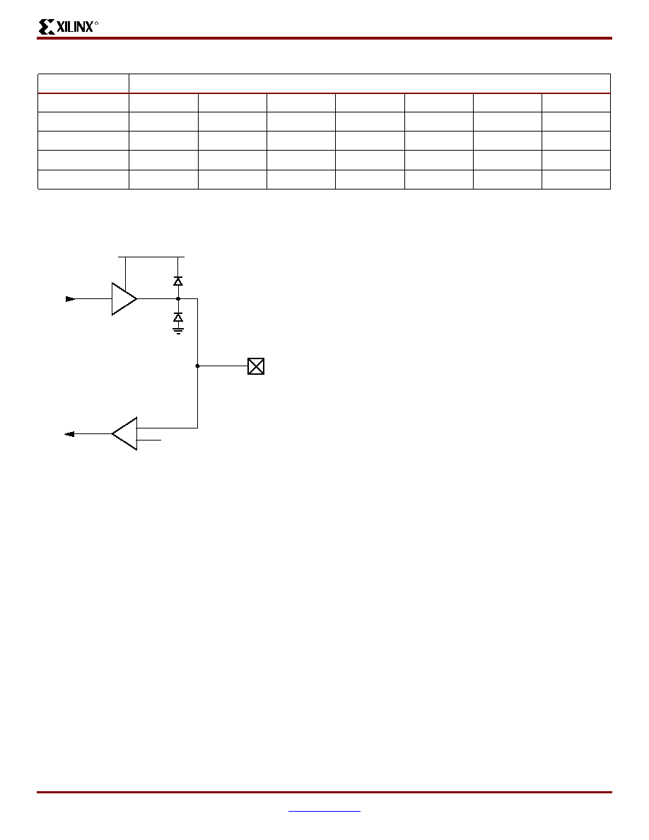
Virtex-II ProTM Platform FPGAs: Functional Description
R
DS083-2 (v2.9) October 14, 2003
www.xilinx.com
17
Advance Product Specification
1-800-255-7778
Figure 14
shows the SSTL2, SSTL18, and HSTL configura-
tions. HSTL can sink current up to 48 mA. (HSTL IV)
All pads are protected against damage from electrostatic
discharge (ESD) and from over-voltage transients.
Virtex-II Pro uses two memory cells to control the configura-
tion of an I/O as an input. This is to reduce the probability of
an I/O configured as an input from flipping to an output
when subjected to a single event upset (SEU) in space
applications.
Prior to configuration, all outputs not involved in configura-
tion are forced into their high-impedance state. The
pull-down resistors and the weak-keeper circuits are inac-
tive. The dedicated pin HSWAP_EN controls the pull-up
resistors prior to configuration. By default, HSWAP_EN is
set High, which disables the pull-up resistors on user I/O
pins. When HSWAP_EN is set Low, the pull-up resistors are
activated on user I/O pins.
All Virtex-II Pro IOBs (except RocketIO transceiver pins)
support IEEE 1149.1 and IEEE 1532 compatible boundary
scan testing.
Input Path
The Virtex-II Pro IOB input path routes input signals directly
to internal logic and / or through an optional input flip-flop or
latch, or through the DDR input registers. An optional delay
element at the D-input of the storage element eliminates
pad-to-pad hold time. The delay is matched to the internal
clock-distribution delay of the Virtex-II Pro device, and when
used, assures that the pad-to-pad hold time is zero.
Each input buffer can be configured to conform to any of the
low-voltage signaling standards supported. In some of
these standards the input buffer utilizes a user-supplied
threshold voltage, V
REF
. The need to supply V
REF
imposes
constraints on which standards can be used in the same
bank. See I/O banking description.
Output Path
The output path includes a 3-state output buffer that drives
the output signal onto the pad. The output and / or the
3-state signal can be routed to the buffer directly from the
internal logic or through an output / 3-state flip-flop or latch,
or through the DDR output / 3-state registers.
Each output driver can be individually programmed for a
wide range of low-voltage signaling standards. In most sig-
naling standards, the output High voltage depends on an
externally supplied V
CCO
voltage. The need to supply V
CCO
imposes constraints on which standards can be used in the
same bank. See I/O banking description.
I/O Banking
Some of the I/O standards described above require V
CCO
and V
REF
voltages. These voltages are externally supplied
and connected to device pins that serve groups of IOB
blocks, called banks. Consequently, restrictions exist about
which I/O standards can be combined within a given bank.
Eight I/O banks result from dividing each edge of the FPGA
into two banks, as shown in
Figure 15
and
Figure 16
. Each
bank has multiple V
CCO
pins, all of which must be con-
nected to the same voltage. This voltage is determined by
the output standards in use.
Table 6: LVCMOS Programmable Currents (Sink and Source)
SelectIO-Ultra
Programmable Current (Worst-Case Guaranteed Minimum)
LVTTL
2 mA
4 mA
6 mA
8 mA
12 mA
16 mA
24 mA
LVCMOS33
2 mA
4 mA
6 mA
8 mA
12 mA
16 mA
24 mA
LVCMOS25
2 mA
4 mA
6 mA
8 mA
12 mA
16 mA
24 mA
LVCMOS18
2 mA
4 mA
6 mA
8 mA
12 mA
16 mA
n/a
LVCMOS15
2 mA
4 mA
6 mA
8 mA
12 mA
16 mA
n/a
Figure 14: SSTL or HSTL SelectIO-Ultra Standards
VCCO
OBUF
VREF
Clamp
Diode
PAD
VCCAUX = 2.5V
VCCINT = 1.5V
DS031_24_100900
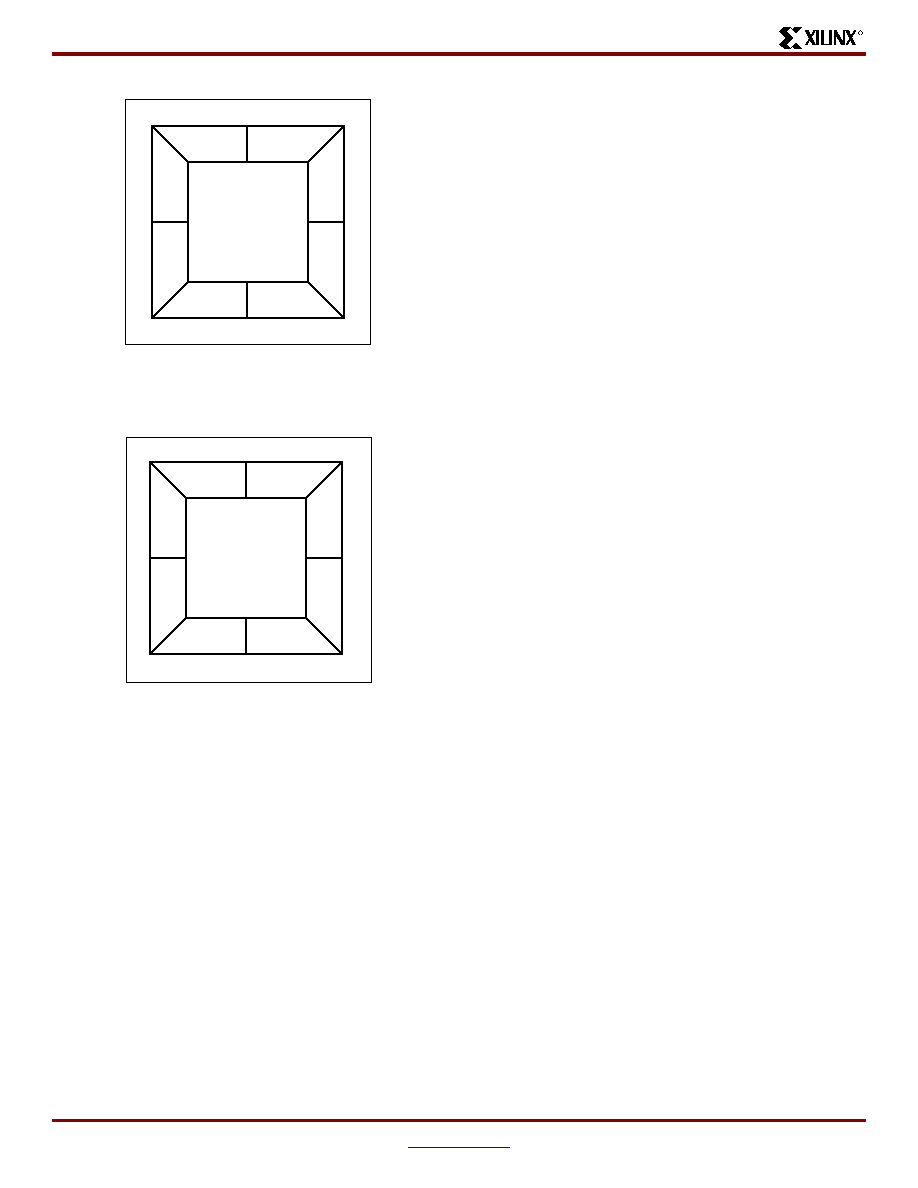
Functional Description: FPGA
R
18
www.xilinx.com
DS083-2 (v2.9) October 14, 2003
1-800-255-7778
Advance Product Specification
Some input standards require a user-supplied threshold
voltage (V
REF
), and certain user-I/O pins are automatically
configured as V
REF
inputs. Approximately one in six of the
I/O pins in the bank assume this role.
V
REF
pins within a bank are interconnected internally, and
thus only one V
REF
voltage can be used within each bank.
However, for correct operation, all V
REF
pins in the bank
must be connected to the external reference voltage source.
The V
CCO
and the V
REF
pins for each bank appear in the
device pinout tables. Within a given package, the number of
V
REF
and V
CCO
pins can vary depending on the size of
device. In larger devices, more I/O pins convert to V
REF
pins. Since these are always a superset of the V
REF
pins
used for smaller devices, it is possible to design a PCB that
permits migration to a larger device if necessary.
All V
REF
pins for the largest device anticipated must be con-
nected to the V
REF
voltage and not used for I/O. In smaller
devices, some V
CCO
pins used in larger devices do not con-
nect within the package. These unconnected pins can be
left unconnected externally, or, if necessary, they can be
connected to V
CCO
to permit migration to a larger device.
Rules for Combining I/O Standards in the Same
Bank
The following rules must be obeyed to combine different
input, output, and bi-directional standards in the same bank:
1.
Combining output standards only. Output standards
with the same output V
CCO
requirement can be
combined in the same bank.
Compatible example:
SSTL2_I and LVDS_25_DCI outputs
Incompatible example:
SSTL2_I (output V
CCO
= 2.5V) and
LVCMOS33 (output V
CCO
= 3.3V) outputs
2.
Combining input standards only. Input standards
with the same input V
CCO
and input V
REF
requirements
can be combined in the same bank.
Compatible example:
LVCMOS15 and HSTL_IV inputs
Incompatible example:
LVCMOS15 (input V
CCO
= 1.5V) and
LVCMOS18 (input V
CCO
= 1.8V) inputs
Incompatible example:
HSTL_I_DCI_18 (V
REF
= 0.9V) and
HSTL_IV_DCI_18 (V
REF
= 1.1V) inputs
3.
Combining input standards and output standards.
Input standards and output standards with the same
input V
CCO
and output V
CCO
requirement can be
combined in the same bank.
Compatible example:
LVDS_25 output and HSTL_I input
Incompatible example:
LVDS_25 output (output V
CCO
= 2.5V) and
HSTL_I_DCI_18 input (input V
CCO
= 1.8V)
4.
Combining bi-directional standards with input or
output standards. When combining bi-directional I/O
with other standards, make sure the bi-directional
standard can meet rules 1 through 3 above.
5.
Additional rules for combining DCI I/O standards.
a.
No more than one Single Termination type (input or
output) is allowed in the same bank.
Incompatible example:
HSTL_IV_DCI input and HSTL_III_DCI input
b.
No more than one Split Termination type (input or
output) is allowed in the same bank.
Incompatible example:
HSTL_I_DCI input and HSTL_II_DCI input
The implementation tools will enforce the above design
rules.
Table 7, page 19
, summarizes all standards and voltage
supplies.
Figure 15: I/O Banks: Wire-Bond Packages (FG) Top
View
Figure 16: I/O Banks: Flip-Chip Packages (FF) Top View
ug002_c2_014_041403
Bank 0
Bank 1
Bank 5
Bank 4
Bank 7
Bank 6
Bank 2
Bank 3
ds031_66_041403
Bank 1
Bank 0
Bank 4
Bank 5
Bank 2
Bank 3
Bank 7
Bank 6
Virtex-II ProTM Platform FPGAs: Functional Description
R
DS083-2 (v2.9) October 14, 2003
www.xilinx.com
19
Advance Product Specification
1-800-255-7778
Digitally Controlled Impedance (DCI)
Today's chip output signals with fast edge rates require ter-
mination to prevent reflections and maintain signal integrity.
High pin count packages (especially ball grid arrays) can
not accommodate external termination resistors.
Virtex-II Pro XCITE DCI provides controlled impedance
drivers and on-chip termination for single-ended and differ-
ential I/Os. This eliminates the need for external resistors
and improves signal integrity. The DCI feature can be used
on any IOB by selecting one of the DCI I/O standards.
When applied to inputs, DCI provides input parallel termina-
tion. When applied to outputs, DCI provides controlled
impedance drivers (series termination) or output parallel
termination.
DCI operates independently on each I/O bank. When a DCI
I/O standard is used in a particular I/O bank, external refer-
ence resistors must be connected to two dual-function pins
on the bank. These resistors, voltage reference of N transis-
tor (VRN) and the voltage reference of P transistor (VRP)
are shown in
Figure 17
.
Table 7: Summary of Voltage Supply Requirements for
All Input and Output Standards
I/O Standard
V
CCO
V
REF
Termination Type
Output
Input
Input
Output
Input
LVTTL
(1)
3.3
3.3
N/R
N/R
N/R
LVCMOS33
(1)
N/R
N/R
N/R
LVDCI_33
(1)
N/R
Series
N/R
PCIX
(2)
N/R
N/R
N/R
PCI33_3
(2)
N/R
N/R
N/R
PCI66_3
(2)
N/R
N/R
N/R
LVDS_25
2.5
Note (3)
N/R
N/R
N/R
LVDSEXT_25
N/R
N/R
N/R
LDT_25
N/R
N/R
N/R
ULVDS_25
N/R
N/R
N/R
BLVDS_25
N/R
N/R
N/R
LVPECL_25
N/R
N/R
N/R
SSTL2_I
1.25
N/R
N/R
SSTL2_II
1.25
N/R
N/R
LVCMOS25
2.5
N/R
N/R
N/R
LVDCI_25
N/R
Series
N/R
LVDCI_DV2_25
N/R
Series
N/R
LVDS_25_DCI
N/R
N/R
Split
LVDSEXT_25_DCI
N/R
N/R
Split
SSTL2_I_DCI
1.25
N/R
Split
SSTL2_II_DCI
1.25
Split
Split
LVDS_25_DT
N/R
N/R
N/R
LVDSEXT_25_DT
N/R
N/R
N/R
LDT_25_DT
N/R
N/R
N/R
ULVDS_25_DT
N/R
N/R
N/R
HSTL_III_18
1.8
Note (3)
1.1
N/R
N/R
HSTL_IV_18
1.1
N/R
N/R
HSTL_I_18
0.9
N/R
N/R
HSTL_II_18
0.9
N/R
N/R
SSTL18_I
0.9
N/R
N/R
SSTL18_II
0.9
N/R
N/R
LVCMOS18
1.8
N/R
N/R
N/R
LVDCI_18
N/R
Series
N/R
LVDCI_DV2_18
N/R
Series
N/R
HSTL_III_DCI_18
1.1
N/R
Single
HSTL_IV_DCI_18
1.1
Single
Single
HSTL_I_DCI_18
0.9
N/R
Split
HSTL_II_DCI_18
0.9
Split
Split
SSTL18_I_DCI
0.9
N/R
Split
SSTL18_II_DCI
0.9
Split
Split
HSTL_III
1.5
Note (3)
0.9
N/R
N/R
HSTL_IV
0.9
N/R
N/R
HSTL_I
0.75
N/R
N/R
HSTL_II
0.75
N/R
N/R
LVCMOS15
1.5
N/R
N/R
N/R
LVDCI_15
N/R
Series
N/R
LVDCI_DV2_15
N/R
Series
N/R
GTLP_DCI
1
Single
Single
HSTL_III_DCI
0.9
N/R
Single
HSTL_IV_DCI
0.9
Single
Single
HSTL_I_DCI
0.75
N/R
Split
HSTL_II_DCI
0.75
Split
Split
GTL_DCI
1.2
1.2
0.8
Single
Single
GTLP
N/R
Note (3)
1
N/R
N/R
GTL
0.8
N/R
N/R
Notes:
1.
See application note
XAPP659
for more detailed information.
2.
See application note
XAPP653
for more detailed information.
3.
Pin voltage must not exceed V
CCO
.
4.
N/R = no requirement.
Table 7: Summary of Voltage Supply Requirements for
All Input and Output Standards (Continued)
I/O Standard
V
CCO
V
REF
Termination Type
Output
Input
Input
Output
Input
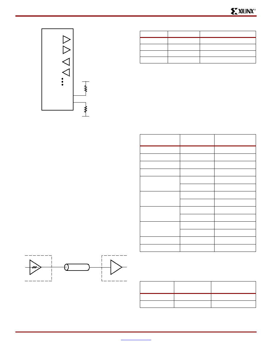
Functional Description: FPGA
R
20
www.xilinx.com
DS083-2 (v2.9) October 14, 2003
1-800-255-7778
Advance Product Specification
When used with a terminated I/O standard, the value of the
resistors are specified by the standard (typically 50
).
When used with a controlled impedance driver, the resistors
set the output impedance of the driver within the specified
range (20
to 100). For all series and parallel termina-
tions listed in
Table 8
and
Table 9
, the reference resistors
must have the same value for any given bank. One percent
resistors are recommended.
The DCI system adjusts the I/O impedance to match the two
external reference resistors, or half of the reference resis-
tors, and compensates for impedance changes due to volt-
age and/or temperature fluctuations. The adjustment is
done by turning parallel transistors in the IOB on or off.
Controlled Impedance Drivers (Series Termination)
DCI can be used to provide a buffer with a controlled output
impedance. It is desirable for this output impedance to
match the transmission line impedance (Z
0
). Virtex-II Pro
input buffers also support LVDCI and LVDCI_DV2 I/O stan-
dards.
Controlled Impedance Terminations
(Parallel Termination)
DCI also provides on-chip termination for SSTL2, SSTL18,
HSTL (Class I, II, III, or IV), LVDS_25, LVDSEXT_25, and
GTL/GTLP receivers or transmitters on bidirectional lines.
Table 9
and
Table 10
list the on-chip parallel terminations
available in Virtex-II Pro devices. V
CCO
must be set accord-
ing to
Table 5
. There is a V
CCO
requirement for GTL_DCI
and GTLP_DCI, due to the on-chip termination resistor.
Figure 17: DCI in a Virtex-II Pro Bank
Figure 18: Internal Series Termination
DS031_50_101200
VCCO
GND
DCI
DCI
DCI
DCI
VRN
VRP
1 Bank
R
REF
(1%)
R
REF
(1%)
Z
0
IOB
Z
Virtex-II Pro DCI
DS083-2_09_082902
V
CCO
= 3.3V, 2.5 V, 1.8 V, or 1.5 V
Table 8: SelectIO-Ultra Controlled Impedance Buffers
V
CCO
DCI
DCI Half Impedance
3.3V
LVDCI_33
N/A
2.5V
LVDCI_25
LVDCI_DV2_25
1.8V
LVDCI_18
LVDCI_DV2_18
1.5V
LVDCI_15
LVDCI_DV2_15
Table 9: SelectIO-Ultra Buffers With On-Chip Parallel
Termination
I/O Standard
External
Termination
On-Chip
Termination
SSTL2 Class I
SSTL2_I
SSTL2_I_DCI
(1)
SSTL2 Class II
SSTL2_II
SSTL2_II_DCI
(1)
SSTL18 Class I
SSTL18_I
SSTL18_I_DCI
SSTL18 Class II
SSTL18_II
SSTL18_II_DCI
HSTL Class I
HSTL_I
HSTL_I_DCI
HSTL_I_18
HSTL_I_DCI_18
HSTL Class II
HSTL_II
HSTL_II_DCI
HSTL_II_18
HSTL_II_DCI_18
HSTL Class III
HSTL_III
HSTL_III_DCI
HSTL_III_18
HSTL_III_DCI_18
HSTL Class IV
HSTL_IV
HSTL_IV_DCI
HSTL_IV_18
HSTL_IV_DCI_18
GTL
GTL
GTL_DCI
GTLP
GTLP
GTLP_DCI
Notes:
1.
SSTL compatible.
Table 10: SelectIO-Ultra Differential Buffers With
On-Chip Termination
I/O Standard
External
Termination
On-Chip Termination
LVDS
LVDS_25 LVDS_25_DCI
LVDSEXT
LVDSEXT_25
LVDSEXT_25_DCI
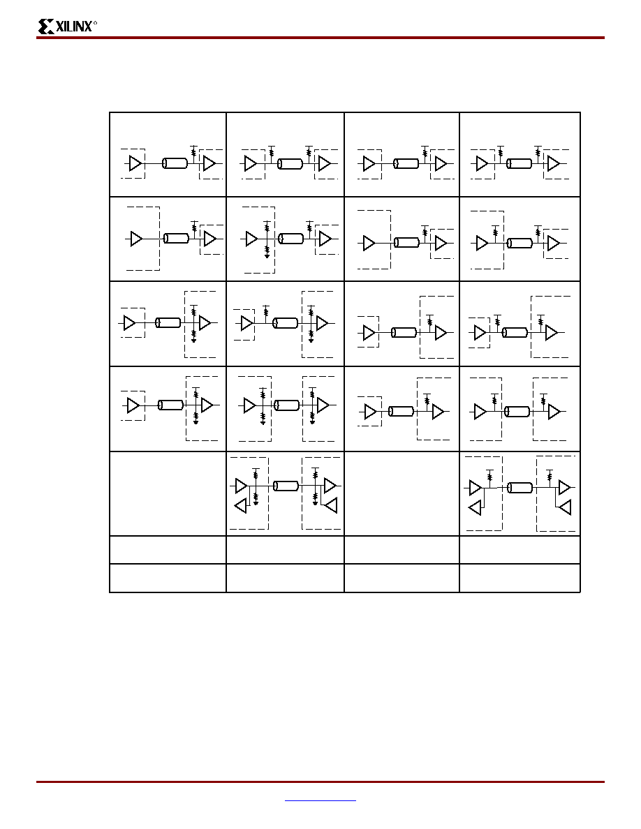
Virtex-II ProTM Platform FPGAs: Functional Description
R
DS083-2 (v2.9) October 14, 2003
www.xilinx.com
21
Advance Product Specification
1-800-255-7778
Figure 19
provides examples illustrating the use of the HSTL_I_DCI, HSTL_II_DCI, HSTL_III_DCI, and HSTL_IV_DCI I/O
standards. For a complete list, see the Virtex-II Pro Platform FPGA User Guide.
Figure 20
provides examples illustrating the use of the SSTL2_I_DCI, SSTL2_II_DCI, SSTL18_I_DCI, and SSTL18_II_DCI
Figure 19: HSTL DCI Usage Examples
R
R
R
R
R
R
R
R
R
R
2R
2R
R
2R
R
2R
2R
2R
2R
2R
DS083-2_65a_082102
Conventional
DCI Transmit
Conventional
Receive
Conventional
Transmit
DCI Receive
DCI Transmit
DCI Receive
Bidirectional
Reference
Resistor
Recommended
Z0
VRN = VRP = R = Z0
50
VRN = VRP = R = Z0
50
VRN = VRP = R = Z0
50
VRN = VRP = R = Z0
50
HSTL_I
HSTL_II
HSTL_III
HSTL_IV
N/A
N/A
R
R
R
R
Z0
R
R
2R
2R
2R
2R
Z0
Z0
Z0
Z0
Z0
Z0
Z0
Z0
Z0
Z0
Z0
Z0
Z0
Z0
Z0
Virtex-II Pro
DCI
Virtex-II Pro
DCI
Virtex-II Pro
DCI
Z0
Virtex-II Pro
DCI
Virtex-II Pro
DCI
Virtex-II Pro
DCI
Virtex-II Pro
DCI
Virtex-II Pro
DCI
Virtex-II Pro
DCI
Virtex-II Pro
DCI
Virtex-II Pro
DCI
Virtex-II Pro
DCI
Virtex-II Pro
DCI
Virtex-II Pro
DCI
Virtex-II Pro
DCI
Virtex-II Pro
DCI
Virtex-II Pro
DCI
Virtex-II Pro
DCI
2R
2R
2R
2R
Z0
R
R
V
CCO
/2
V
CCO
/2
V
CCO
/2
V
CCO
/2
V
CCO
/2
V
CCO
/2
V
CCO
V
CCO
V
CCO
V
CCO
V
CCO
V
CCO
V
CCO
V
CCO
V
CCO
V
CCO
V
CCO
V
CCO
V
CCO
V
CCO
V
CCO
V
CCO
V
CCO
V
CCO
V
CCO
V
CCO
V
CCO
V
CCO
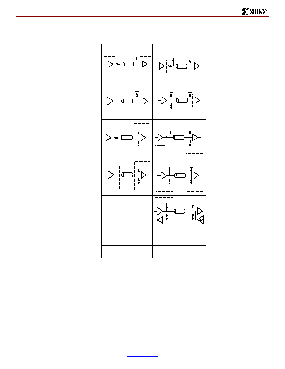
Functional Description: FPGA
R
22
www.xilinx.com
DS083-2 (v2.9) October 14, 2003
1-800-255-7778
Advance Product Specification
I/O standards. For a complete list, see the Virtex-II Pro Platform FPGA User Guide.
Figure 20: SSTL DCI Usage Examples
DS083-2_65b_011603
Conventional
DCI Transmit
Conventional
Receive
Conventional
Transmit
DCI Receive
DCI Transmit
DCI Receive
Bidirectional
Reference
Resistor
Recommended
Z0
(2)
VRN = VRP = R = Z0
50
VRN = VRP = R = Z0
50
SSTL2_I or SSTL18_I
SSTL2_II or SSTL18_II
N/A
Z0
R
V
CCO
/2
Z0
R/2
R
R
V
CCO
/2
V
CCO
/2
Z0
R/2
R
V
CCO
/2
Z0
R/2
2R
2R
V
CCO
Z0
R/2
2R
2R
V
CCO
2R
R
V
CCO
V
CCO
/2
2R
Z0
R
V
CCO
/2
Z0
2R
2R
V
CCO
2R
2R
V
CCO
Z0
2R
2R
V
CCO
Z0
2R
2R
V
CCO
2R
2R
V
CCO
25
(1)
25
(1)
25
(1)
25
(1)
25
(1)
25
Virtex-II Pro
DCI
Virtex-II Pro
DCI
Virtex-II Pro
DCI
Virtex-II Pro
DCI
Virtex-II Pro
DCI
Virtex-II Pro
DCI
Virtex-II Pro
DCI
Virtex-II Pro
DCI
Virtex-II Pro
DCI
Virtex-II Pro
DCI
Notes:
1. The SSTL-compatible 25
series resistor is accounted for in the DCI buffer,
and it is not DCI controlled.
2. Z0 is the recommended PCB trace impedance.
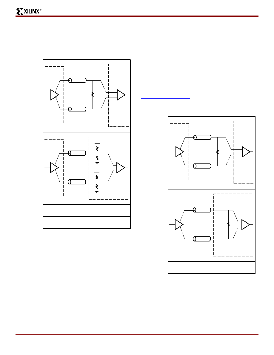
Virtex-II ProTM Platform FPGAs: Functional Description
R
DS083-2 (v2.9) October 14, 2003
www.xilinx.com
23
Advance Product Specification
1-800-255-7778
Figure 21
provides examples illustrating the use of the
LVDS_25_DCI and LVDSEXT_25_DCI I/O standards. For a
complete list, see the Virtex-II Pro Platform FPGA User
Guide.
On-Chip Differential Termination
Virtex-II Pro provides a true 100
differential termination
(DT) across the input differential receiver terminals. The
LVDS_25_DT, LVDSEXT_25_DT, LDT_25_DT, and
ULVDS_25_DT standards support on-chip differential termi-
nation.
The on-chip input differential termination in Virtex-II Pro
provides major advantages over the external resistor or the
DCI termination solution:
∑
Eliminates the stub at the receiver completely and
therefore greatly improve signal integrity
∑
Consumes less power than DCI termination
∑
Supports LDT (not supported by DCI termination)
∑
Frees up VRP/VRN pins
Figure 22
provides examples illustrating the use of the
LVDS_25_DT, LVDSEXT_25_DT, LDT_25_DT, and
ULVDS_25_DT I/O standards. For further details, refer to
Solution Record 17244
. Also see the
Virtex-II Pro Plat-
form FPGA User Guide
for more design information.
Figure 21: LVDS DCI Usage Examples
DS083-2_65c_022103
Conventional
Conventional
Transmit
DCI Receive
Reference
Resistor
Recommended
Z0
VRN = VRP = R = Z0
50
LVDS_25_DCI and LVDSEXT_25_DCI Receiver
Virtex-II Pro
LVDS DCI
Z0
2R
2R
V
CCO
Z0
2R
2R
V
CCO
Virtex-II Pro
LVDS
Z0
2R
Z0
NOTE: Only LVDS25_DCI is supported (V
CCO
= 2.5V only)
Figure 22: LVDS Differential Termination Usage
Examples
DS083-2_65e_052703
Conventional
Conventional
Transmit,
On-Chip
Differential
Termination
Receive
Recommended
Z0
50
LVDS_25_DT, LVDSEXT_25_DT,
LDT_25_DT, and ULVDS_25_DT Receiver
Virtex-II Pro
LVDS On-Chip
Differential
Termination
Z0
100
Z0
Virtex-II Pro
LVDS
Z0
2R
Z0
NOTE: Only 2.5V LVDS standards are supported (V
CCO
= 2.5V only)
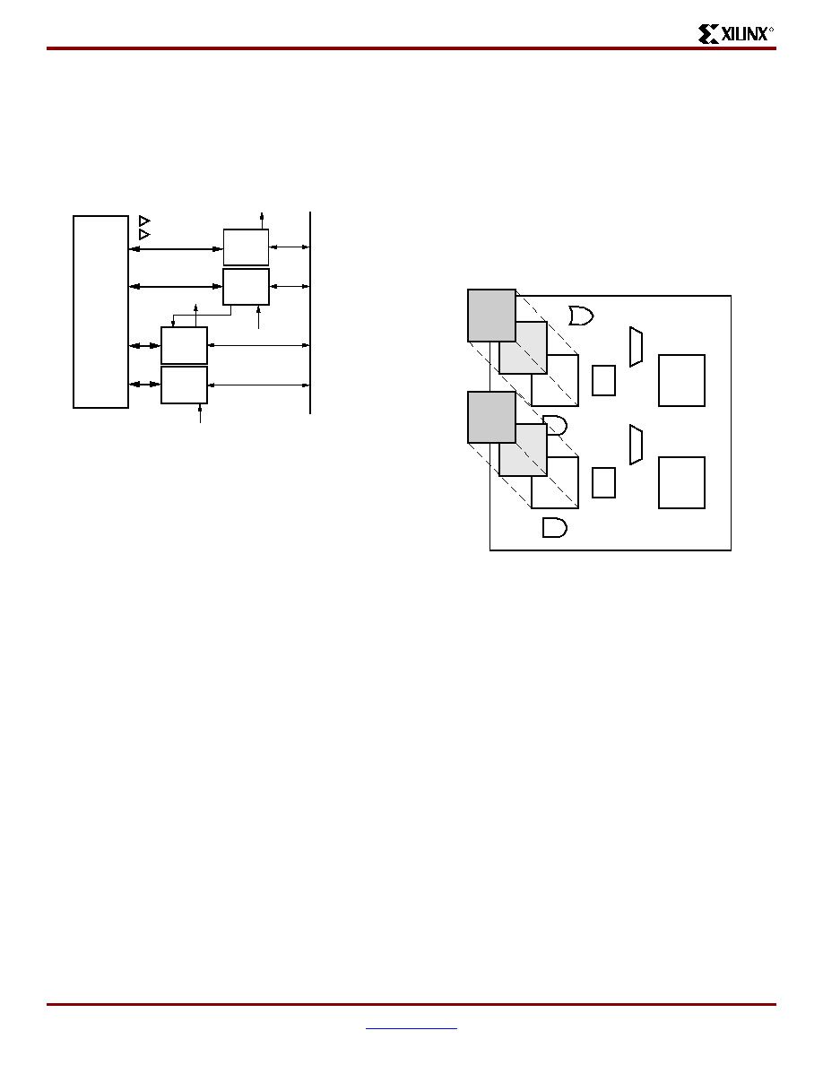
Functional Description: FPGA
R
24
www.xilinx.com
DS083-2 (v2.9) October 14, 2003
1-800-255-7778
Advance Product Specification
Configurable Logic Blocks (CLBs)
The Virtex-II Pro configurable logic blocks (CLB) are orga-
nized in an array and are used to build combinatorial and
synchronous logic designs. Each CLB element is tied to a
switch matrix to access the general routing matrix, as
shown in
Figure 23
.
A CLB element comprises 4 similar slices, with fast local
feedback within the CLB. The four slices are split in two col-
umns of two slices with two independent carry logic chains
and one common shift chain.
Slice Description
Each slice includes two 4-input function generators, carry
logic, arithmetic logic gates, wide function multiplexers and
two storage elements. As shown in
Figure 24
, each 4-input
function generator is programmable as a 4-input LUT, 16
bits of distributed SelectRAM+ memory, or a 16-bit vari-
able-tap shift register element.
Figure 23: Virtex-II Pro CLB Element
Slice
X1Y1
Slice
X1Y0
Slice
X0Y1
Slice
X0Y0
Fast
Connects
to neighbors
Switch
Matrix
DS083-2_32_122001
SHIFT
CIN
COUT
TBUF
COUT
CIN
TBUF
Figure 24: Virtex-II Pro Slice Configuration
Register/
Latch
MUXF5
MUXFx
CY
SRL16
RAM16
LUT
G
Register/
Latch
Arithmetic Logic
CY
LUT
F
DS083-2_31_122001
SRL16
RAM16
ORCY
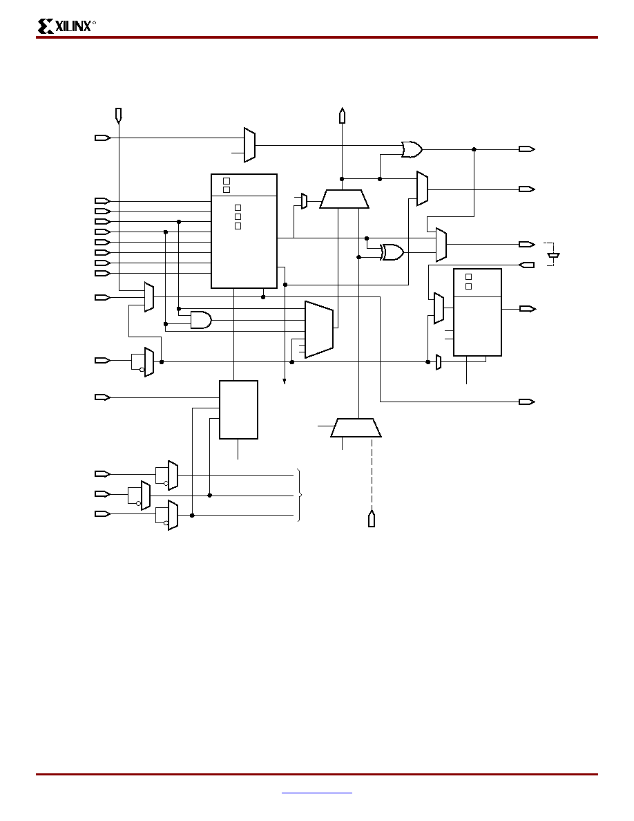
Virtex-II ProTM Platform FPGAs: Functional Description
R
DS083-2 (v2.9) October 14, 2003
www.xilinx.com
25
Advance Product Specification
1-800-255-7778
The output from the function generator in each slice drives both the slice output and the D input of the storage element.
Figure 25
shows a more detailed view of a single slice.
Configurations
Look-Up Table
Virtex-II Pro function generators are implemented as
4-input look-up tables (LUTs). Four independent inputs are
provided to each of the two function generators in a slice (F
and G). These function generators are each capable of
implementing any arbitrarily defined boolean function of four
inputs. The propagation delay is therefore independent of
the function implemented. Signals from the function gener-
ators can exit the slice (X or Y output), can input the XOR
dedicated gate (see arithmetic logic), or input the carry-logic
multiplexer (see fast look-ahead carry logic), or feed the D
input of the storage element, or go to the MUXF5 (not
shown in
Figure 25
).
In addition to the basic LUTs, the Virtex-II Pro slice contains
logic (MUXF5 and MUXFX multiplexers) that combines
function generators to provide any function of five, six,
seven, or eight inputs. The MUXFX is either MUXF6,
MUXF7, or MUXF8 according to the slice considered in the
CLB. Selected functions up to nine inputs (MUXF5 multi-
plexer) can be implemented in one slice. The MUXFX can
also be a MUXF6, MUXF7, or MUXF8 multiplexer to map
any function of six, seven, or eight inputs and selected wide
logic functions.
Register/Latch
The storage elements in a Virtex-II Pro slice can be config-
ured either as edge-triggered D-type flip-flops or as
level-sensitive latches. The D input can be directly driven by
Figure 25: Virtex-II Pro Slice (Top Half)
G4
SOPIN
A4
G3
A3
G2
A2
G1
A1
WG4
WG4
WG3
WG3
WG2
WG2
WG1
BY
WG1
Dual-Port
LUT
FF
LATCH
RAM
ROM
Shift-Reg
D
0
MC15
WS
SR
SR
REV
DI
G
Y
G2
G1
BY
1
0
PROD
D
Q
CE
CE
CK
CLK
MUXCY
YB
DIG
DY
Y
0
1
MUXCY
0
1
1
SOPOUT
DYMUX
GYMUX
YBMUX
ORCY
WSG
WE[2:0]
SHIFTOUT
CYOG
XORG
WE
CLK
WSF
ALTDIG
CE
SR
CLK
SLICEWE[2:0]
MULTAND
Shared between
x & y Registers
SHIFTIN
COUT
CIN
DS031_01_112502
Q
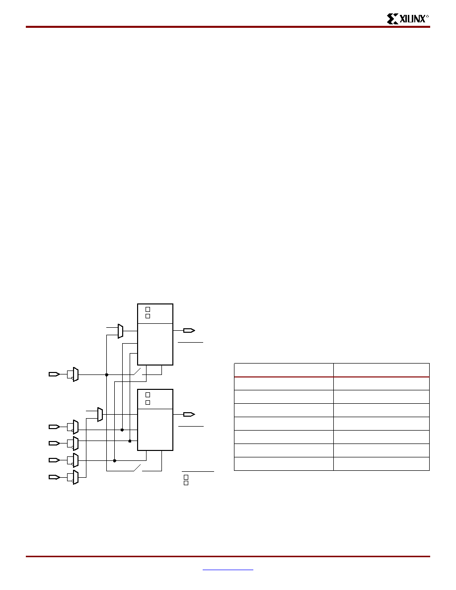
Functional Description: FPGA
R
26
www.xilinx.com
DS083-2 (v2.9) October 14, 2003
1-800-255-7778
Advance Product Specification
the X or Y output via the DX or DY input, or by the slice
inputs bypassing the function generators via the BX or BY
input. The clock enable signal (CE) is active High by default.
If left unconnected, the clock enable for that storage ele-
ment defaults to the active state.
In addition to clock (CK) and clock enable (CE) signals,
each slice has set and reset signals (SR and BY slice
inputs). SR forces the storage element into the state speci-
fied by the attribute SRHIGH or SRLOW. SRHIGH forces a
logic 1 when SR is asserted. SRLOW forces a logic 0. When
SR is used, an optional second input (BY) forces the stor-
age element into the opposite state via the REV pin. The
reset condition is predominant over the set condition. (See
Figure 26
.)
The initial state after configuration or global initial state is
defined by a separate INIT0 and INIT1 attribute. By default,
setting the SRLOW attribute sets INIT0, and setting the
SRHIGH attribute sets INIT1.
For each slice, set and reset can be set to be synchronous
or asynchronous. Virtex-II Pro devices also have the ability
to set INIT0 and INIT1 independent of SRHIGH and
SRLOW.
The control signals clock (CLK), clock enable (CE) and
set/reset (SR) are common to both storage elements in one
slice. All of the control signals have independent polarity. Any
inverter placed on a control input is automatically absorbed.
The set and reset functionality of a register or a latch can be
configured as follows:
∑
No set or reset
∑
Synchronous set
∑
Synchronous reset
∑
Synchronous set and reset
∑
Asynchronous set (preset)
∑
Asynchronous reset (clear)
∑
Asynchronous set and reset (preset and clear)
The synchronous reset has precedence over a set, and an
asynchronous clear has precedence over a preset.
Distributed SelectRAM+ Memory
Each function generator (LUT) can implement a 16 x 1-bit
synchronous RAM resource called a distributed
SelectRAM+ element. SelectRAM+ elements are config-
urable within a CLB to implement the following:
∑
Single-Port 16 x 8-bit RAM
∑
Single-Port 32 x 4-bit RAM
∑
Single-Port 64 x 2-bit RAM
∑
Single-Port 128 x 1-bit RAM
∑
Dual-Port 16 x 4-bit RAM
∑
Dual-Port 32 x 2-bit RAM
∑
Dual-Port 64 x 1-bit RAM
Distributed SelectRAM+ memory modules are synchronous
(write) resources. The combinatorial read access time is
extremely fast, while the synchronous write simplifies
high-speed designs. A synchronous read can be imple-
mented with a storage element in the same slice. The dis-
tributed SelectRAM+ memory and the storage element
share the same clock input. A Write Enable (WE) input is
active High, and is driven by the SR input.
Table 11
shows the number of LUTs (2 per slice) occupied
by each distributed SelectRAM+ configuration.
For single-port configurations, distributed SelectRAM+
memory has one address port for synchronous writes and
asynchronous reads.
For dual-port configurations, distributed SelectRAM+ mem-
ory has one port for synchronous writes and asynchronous
Figure 26: Register / Latch Configuration in a Slice
FF
FFY
LATCH
SR REV
D
Q
CE
CK
YQ
FF
FFX
LATCH
SR REV
D
Q
CE
CK
XQ
CE
DX
DY
BY
CLK
BX
SR
Attribute
INIT1
INIT0
SRHIGH
SRLOW
Attribute
INIT1
INIT0
SRHIGH
SRLOW
Reset Type
SYNC
ASYNC
DS083-2_22_122001
Table 11: Distributed SelectRAM+ Configurations
RAM
Number of LUTs
16 x 1S
1
16 x 1D
2
32 x 1S
2
32 x 1D
4
64 x 1S
4
64 x 1D
8
128 x 1S
8
Notes:
1.
S = single-port configuration; D = dual-port configuration
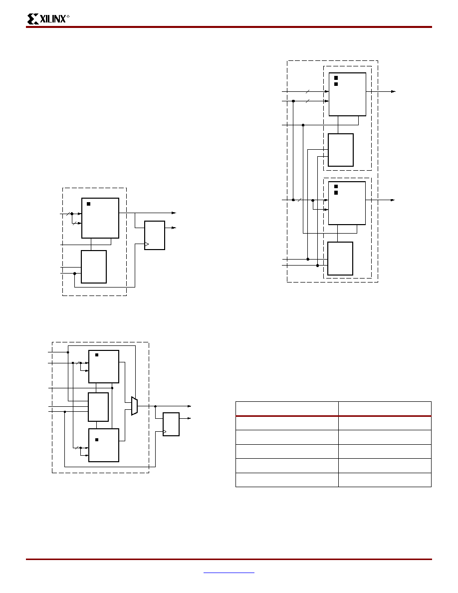
Virtex-II ProTM Platform FPGAs: Functional Description
R
DS083-2 (v2.9) October 14, 2003
www.xilinx.com
27
Advance Product Specification
1-800-255-7778
reads and another port for asynchronous reads. The func-
tion generator (LUT) has separated read address inputs
(A1, A2, A3, A4) and write address inputs (WG1/WF1,
WG2/WF2, WG3/WF3, WG4/WF4).
In single-port mode, read and write addresses share the
same address bus. In dual-port mode, one function genera-
tor (R/W port) is connected with shared read and write
addresses. The second function generator has the A inputs
(read) connected to the second read-only port address and
the W inputs (write) shared with the first read/write port
address.
Figure 27
,
Figure 28
, and
Figure 29
illustrate various exam-
ple configurations.
Similar to the RAM configuration, each function generator
(LUT) can implement a 16 x 1-bit ROM. Five configurations
are available: ROM16x1, ROM32x1, ROM64x1,
ROM128x1, and ROM256x1. The ROM elements are cas-
cadable to implement wider or/and deeper ROM. ROM con-
tents are loaded at configuration.
Table 12
shows the
number of LUTs occupied by each configuration.
Figure 27: Distributed SelectRAM+ (RAM16x1S)
Figure 28: Single-Port Distributed SelectRAM+
(RAM32x1S)
A[3:0]
D
D
DI
WS
WSG
WE
WCLK
RAM 16x1S
D
Q
RAM
WE
CK
A[4:1]
WG[4:1]
Output
Registered
Output
(optional)
(SR)
4
4
(BY)
DS031_02_100900
A[3:0]
D
WSG
F5MUX
WE
WCLK
RAM 32x1S
D
Q
WE
WE0
CK
WSF
D
DI
WS
RAM
G[4:1]
A[4]
WG[4:1]
D
DI
WS
RAM
F[4:1]
WF[4:1]
Output
Registered
Output
(optional)
(SR)
4
(BY)
(BX)
4
DS083-2_10_050901
Figure 29: Dual-Port Distributed SelectRAM+
(RAM16x1D)
Table 12: ROM Configuration
ROM
Number of LUTs
16 x 1
1
32 x 1
2
64 x 1
4
128 x 1
8 (1 CLB)
256 x 1
16 (2 CLBs)
A[3:0]
D
WSG
WE
WCLK
RAM 16x1D
WE
CK
D
DI
WS
RAM
G[4:1]
WG[4:1]
dual_port
RAM
dual_port
4
(BY)
DPRA[3:0]
SPO
A[3:0]
WSG
WE
CK
D
DI
WS
G[4:1]
WG[4:1]
DPO
4
4
DS031_04_110100
(SR)

Functional Description: FPGA
R
28
www.xilinx.com
DS083-2 (v2.9) October 14, 2003
1-800-255-7778
Advance Product Specification
Shift Registers
Each function generator can also be configured as a 16-bit
shift register. The write operation is synchronous with a
clock input (CLK) and an optional clock enable, as shown in
Figure 30
. A dynamic read access is performed through the
4-bit address bus, A[3:0]. The configurable 16-bit shift regis-
ter cannot be set or reset. The read is asynchronous; how-
ever, the storage element or flip-flop is available to
implement a synchronous read. Any of the 16 bits can be
read out asynchronously by varying the address. The stor-
age element should always be used with a constant
address. For example, when building an 8-bit shift register
and configuring the addresses to point to the 7th bit, the 8th
bit can be the flip-flop. The overall system performance is
improved by using the superior clock-to-out of the flip-flops.
An additional dedicated connection between shift registers
allows connecting the last bit of one shift register to the first
bit of the next, without using the ordinary LUT output. (See
Figure 31
.) Longer shift registers can be built with dynamic
access to any bit in the chain. The shift register chaining
and the MUXF5, MUXF6, and MUXF7 multiplexers allow up
to a 128-bit shift register with addressable access to be
implemented in one CLB.
Figure 30: Shift Register Configurations
A[3:0]
SHIFTIN
SHIFTOUT
D(BY)
D
MC15
DI
WSG
CE (SR)
CLK
SRLC16
D
Q
SHIFT-REG
WE
CK
A[4:1]
Output
Registered
Output
(optional)
4
DS031_05_110600
WS
Figure 31: Cascadable Shift Register
SRLC16
MC15
MC15
D
SRLC16
DI
SHIFTIN
CASCADABLE OUT
SLICE S0
SLICE S1
SLICE S2
SLICE S3
1 Shift Chain
in CLB
CLB
DS031_06_110200
FF
FF
D
SRLC16
MC15
MC15
D
SRLC16
DI
SHIFTIN
SHIFTOUT
FF
FF
D
SRLC16
MC15
MC15
D
SRLC16
DI
DI
SHIFTIN
IN
SHIFTOUT
FF
FF
D
SRLC16
MC15
MC15
D
SRLC16
DI
SHIFTOUT
FF
FF
D
DI
DI
DI
OUT
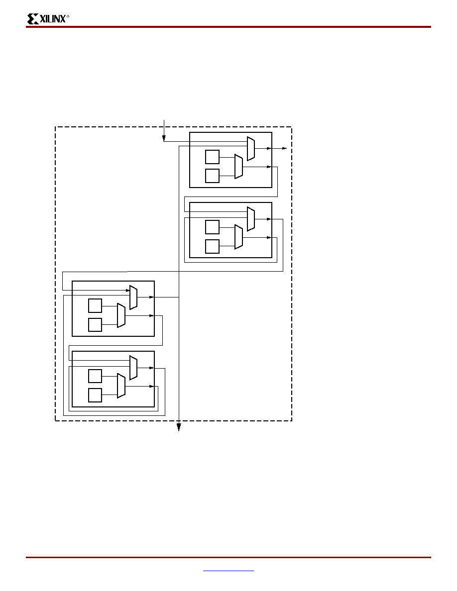
Virtex-II ProTM Platform FPGAs: Functional Description
R
DS083-2 (v2.9) October 14, 2003
www.xilinx.com
29
Advance Product Specification
1-800-255-7778
Multiplexers
Virtex-II Pro function generators and associated multiplex-
ers can implement the following:
∑
4:1 multiplexer in one slice
∑
8:1 multiplexer in two slices
∑
16:1 multiplexer in one CLB element (4 slices)
∑
32:1 multiplexer in two CLB elements (8 slices)
Each Virtex-II Pro slice has one MUXF5 multiplexer and
one MUXFX multiplexer. The MUXFX multiplexer imple-
ments the MUXF6, MUXF7, or MUXF8, as shown in
Figure 32
. Each CLB element has two MUXF6 multiplexers,
one MUXF7 multiplexer and one MUXF8 multiplexer. Exam-
ples of multiplexers are shown in the Virtex-II Pro Platform
FPGA User Guide. Any LUT can implement a 2:1 multi-
plexer.
Fast Lookahead Carry Logic
Dedicated carry logic provides fast arithmetic addition and
subtraction. The Virtex-II Pro CLB has two separate carry
chains, as shown in the
Figure 33
.
The height of the carry chains is two bits per slice. The carry
chain in the Virtex-II Pro device is running upward. The ded-
icated carry path and carry multiplexer (MUXCY) can also
be used to cascade function generators for implementing
wide logic functions.
Figure 32: MUXF5 and MUXFX multiplexers
Slice S1
Slice S0
Slice S3
Slice S2
CLB
DS031_08_110200
F5
F6
F5
F7
F5
F6
F5
F8
MUXF8 combines
the two MUXF7 outputs
(Two CLBs)
MUXF6 combines the two MUXF5
outputs from slices S2 and S3
MUXF7 combines the two MUXF6
outputs from slices S0 and S2
MUXF6 combines the two MUXF6
outputs from slices S0 and S1
G
F
G
F
G
F
G
F
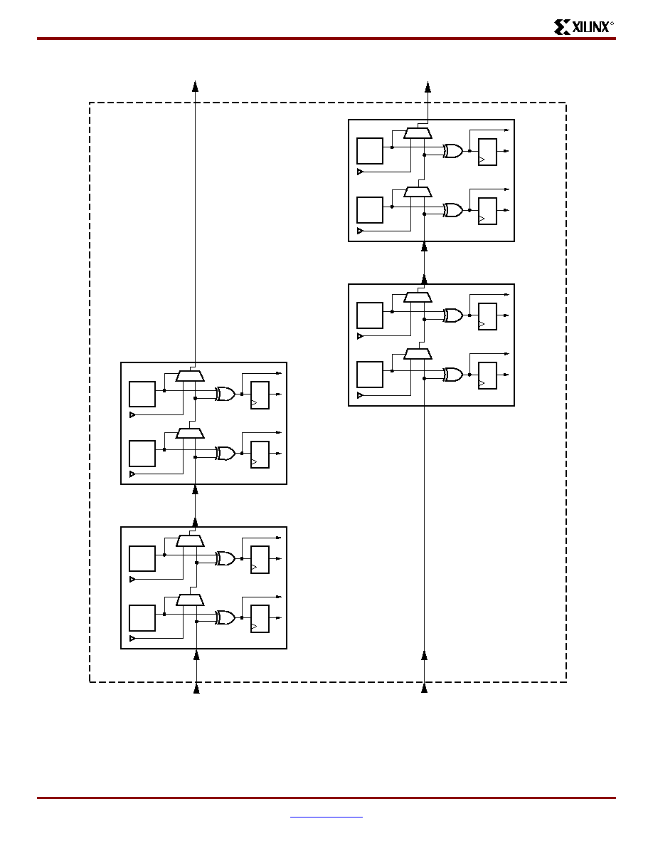
Functional Description: FPGA
R
30
www.xilinx.com
DS083-2 (v2.9) October 14, 2003
1-800-255-7778
Advance Product Specification
Arithmetic Logic
The arithmetic logic includes an XOR gate that allows a
2-bit full adder to be implemented within a slice. In addition,
a dedicated AND (MULT_AND) gate (shown in
Figure 25
)
improves the efficiency of multiplier implementation.
Figure 33: Fast Carry Logic Path
FF
LUT
O I
MUXCY
FF
LUT
O I
MUXCY
FF
LUT
O I
MUXCY
FF
LUT
O I
MUXCY
CIN
CIN
CIN
COUT
FF
LUT
O I
MUXCY
FF
LUT
O I
MUXCY
FF
LUT
O I
MUXCY
FF
LUT
O I
MUXCY
CIN
COUT
COUT
to CIN of S2 of the next CLB
COUT
to S0 of the next CLB
(First Carry Chain)
(Second Carry Chain)
SLICE S1
SLICE S0
SLICE S3
SLICE S2
CLB
DS031_07_110200
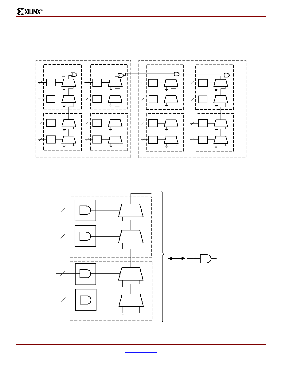
Virtex-II ProTM Platform FPGAs: Functional Description
R
DS083-2 (v2.9) October 14, 2003
www.xilinx.com
31
Advance Product Specification
1-800-255-7778
Sum of Products
Each Virtex-II Pro slice has a dedicated OR gate named
ORCY, ORing together outputs from the slices carryout and
the ORCY from an adjacent slice. The ORCY gate with the
dedicated Sum of Products (SOP) chain are designed for
implementing large, flexible SOP chains. One input of each
ORCY is connected through the fast SOP chain to the output
of the previous ORCY in the same slice row. The second input
is connected to the output of the top MUXCY in the same slice,
as shown in
Figure 34
.
LUTs and MUXCYs can implement large AND gates or
other combinatorial logic functions.
Figure 35
illustrates
LUT and MUXCY resources configured as a 16-input AND
gate.
Figure 34: Horizontal Cascade Chain
MUXCY
4
MUXCY
4
Slice 1
ds031_64_110300
ORCY
LUT
LUT
MUXCY
4
MUXCY
4
Slice 0
V
CC
LUT
LUT
MUXCY
4
MUXCY
4
Slice 3
ORCY
LUT
LUT
MUXCY
4
MUXCY
4
Slice 2
V
CC
LUT
LUT
SOP
CLB
MUXCY
4
MUXCY
4
Slice 1
ORCY
LUT
LUT
MUXCY
4
MUXCY
4
Slice 0
V
CC
LUT
LUT
MUXCY
4
MUXCY
4
Slice 3
ORCY
LUT
LUT
MUXCY
4
MUXCY
4
Slice 2
V
CC
LUT
LUT
CLB
Figure 35: Wide-Input AND Gate (16 Inputs)
MUXCY
AND
4
16
MUXCY
4
"0"
0
1
0
1
"0"
0
1
"0"
MUXCY
4
Slice
OUT
OUT
Slice
LUT
DS031_41_110600
LUT
LUT
V
CC
MUXCY
4
0
1
LUT
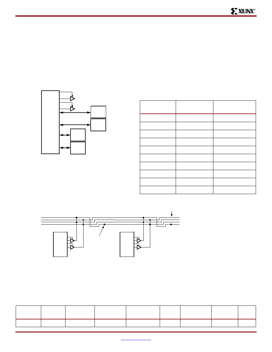
Functional Description: FPGA
R
32
www.xilinx.com
DS083-2 (v2.9) October 14, 2003
1-800-255-7778
Advance Product Specification
3-State Buffers
Introduction
Each Virtex-II Pro CLB contains two 3-state drivers
(TBUFs) that can drive on-chip buses. Each 3-state buffer
has its own 3-state control pin and its own input pin.
Each of the four slices have access to the two 3-state buff-
ers through the switch matrix, as shown in
Figure 36
.
TBUFs in neighboring CLBs can access slice outputs by
direct connects. The outputs of the 3-state buffers drive hor-
izontal routing resources used to implement 3-state buses.
The 3-state buffer logic is implemented using AND-OR logic
rather than 3-state drivers, so that timing is more predict-
able and less load dependant especially with larger devices.
Locations / Organization
Four horizontal routing resources per CLB are provided for
on-chip 3-state buses. Each 3-state buffer has access alter-
nately to two horizontal lines, which can be partitioned as
shown in
Figure 37
. The switch matrices corresponding to
SelectRAM+ memory and multiplier or I/O blocks are
skipped.
Number of 3-State Buffers
Table 13
shows the number of 3-state buffers available in
each Virtex-II Pro device. The number of 3-state buffers is
twice the number of CLB elements.
CLB/Slice Configurations
Table 14
summarizes the logic resources in one CLB. All of
the CLBs are identical and each CLB or slice can be imple-
mented in one of the configurations listed.
Table 15
shows
the available resources in all CLBs.
Figure 36: Virtex-II Pro 3-State Buffers
Slice
S3
Slice
S2
Slice
S1
Slice
S0
Switch
Matrix
DS031_37_060700
TBUF
TBUF
Table 13: Virtex-II Pro 3-State Buffers
Device
3-State Buffers
per Row
Total Number
of 3-State Buffers
XC2VP2
44
704
XC2VP4
44
1,760
XC2VP7
68
2,720
XC2VP20
92
5,152
XC2VP30
92
6,848
XC2VP40
116
9,696
XC2VP50
140
11,808
XC2VP70
164
16,544
XC2VP100
188
22,048
XC2VP125
212
27,808
Figure 37: 3-State Buffer Connection to Horizontal Lines
Switch
matrix
CLB-II
Switch
matrix
CLB-II
DS031_09_032700
Programmable
connection
3 - state lines
Table 14: Logic Resources in One CLB
Slices
LUTs
Flip-Flops
MULT_ANDs
Arithmetic &
Carry-Chains
SOP
Chains
Distributed
SelectRAM+
Shift
Registers
TBUF
4
8
8
8
2
2
128 bits
128 bits
2

Virtex-II ProTM Platform FPGAs: Functional Description
R
DS083-2 (v2.9) October 14, 2003
www.xilinx.com
33
Advance Product Specification
1-800-255-7778
18 Kb Block SelectRAM+
Resources
Introduction
Virtex-II Pro devices incorporate large amounts of 18 Kb
block SelectRAM+ resources. These complement the dis-
tributed SelectRAM+ resources that provide shallow RAM
structures implemented in CLBs. Each Virtex-II Pro block
SelectRAM+ resource is an 18 Kb true dual-port RAM with
two independently clocked and independently controlled
synchronous ports that access a common storage area.
Both ports are functionally identical. CLK, EN, WE, and
SSR polarities are defined through configuration.
Each port has the following types of inputs: Clock and Clock
Enable, Write Enable, Set/Reset, and Address, as well as
separate Data/parity data inputs (for write) and Data/parity
data outputs (for read).
Operation is synchronous; the block SelectRAM+ behaves
like a register. Control, address and data inputs must (and
need only) be valid during the set-up time window prior to a
rising (or falling, a configuration option) clock edge. Data
outputs change as a result of the same clock edge.
Configuration
Virtex-II Pro block SelectRAM+ supports various configura-
tions, including single- and dual-port RAM and various
data/address aspect ratios. Supported memory configura-
tions for single- and dual-port modes are shown in
Table 16
.
Single-Port Configuration
As a single-port RAM, the block SelectRAM+ has access to
the 18 Kb memory locations in any of the 2K x 9-bit,
1K x 18-bit, or 512 x 36-bit configurations and to 16 Kb
memory locations in any of the 16K x 1-bit, 8K x 2-bit, or
4K x 4-bit configurations. The advantage of the 9-bit, 18-bit
and 36-bit widths is the ability to store a parity bit for each
eight bits. Parity bits must be generated or checked exter-
nally in user logic. In such cases, the width is viewed as
8 + 1, 16 + 2, or 32 + 4. These extra parity bits are stored
and behave exactly as the other bits, including the timing
parameters. Video applications can use the 9-bit ratio of
Virtex-II Pro block SelectRAM+ memory to advantage.
Each block SelectRAM+ cell is a fully synchronous memory
as illustrated in
Figure 38
. Input data bus and output data
bus widths are identical.
Table 15: Virtex-II Pro Logic Resources Available in All CLBs
Device
CLB Array:
Row x
Column
Number
of
Slices
Number
of LUTs
Max Distributed
SelectRAM+ or
Shift Register
(bits)
Number of
Flip-Flops
Number of
Carry Chains
(1)
Number
of SOP
Chains
(1)
XC2VP2
16 x 22
1,408
2,816
45,056
2,816
44
32
XC2VP4
40 x 22
3,008
6,016
96,256
6,016
44
80
XC2VP7
40 x 34
4,928
9,856
157,696
9,856
68
80
XC2VP20
56 x 46
9,280
18,560
296,960
18,560
92
112
XC2VP30
80 x 46
13,696
27,392
438,272
27,392
92
160
XC2VP40
88 x 58
19,392
38,784
620,544
38,784
116
176
XC2VP50
88 x 70
23,616
47,232
755,712
47,232
140
176
XC2VP70
104 x 82
33,088
66,176
1,058,816
66,176
164
208
XC2VP100
120 x 94
44,096
88,192
1,411,072
88,192
188
240
XC2VP125
136 x 106
55,616
111,232
1,779,712
111,232
212
272
Notes:
1.
The carry-chains and SOP chains can be split or cascaded.
Table 16: Dual- and Single-Port Configurations
16K x 1 bit
2K x 9 bits
8K x 2 bits
1K x 18 bits
4K x 4 bits
512 x 36 bits
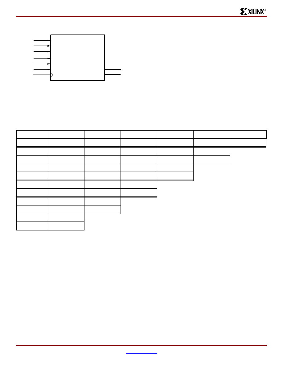
Functional Description: FPGA
R
34
www.xilinx.com
DS083-2 (v2.9) October 14, 2003
1-800-255-7778
Advance Product Specification
Dual-Port Configuration
As a dual-port RAM, each port of block SelectRAM+ has
access to a common 18 Kb memory resource. These are
fully synchronous ports with independent control signals for
each port. The data widths of the two ports can be config-
ured independently, providing built-in bus-width conversion.
Table 17
illustrates the different configurations available on
ports A and B.
If both ports are configured in either 2K x 9-bit, 1K x 18-bit,
or 512 x 36-bit configurations, the 18 Kb block is accessible
from port A or B. If both ports are configured in either 16K x
1-bit, 8K x 2-bit. or 4K x 4-bit configurations, the 16 K-bit
block is accessible from Port A or Port B. All other configu-
rations result in one port having access to an 18 Kb memory
block and the other port having access to a 16 K-bit subset
of the memory block equal to 16 Kbs.
Figure 38: 18 Kb Block SelectRAM+ Memory in
Single-Port Mode
DOP
DIP
ADDR
WE
EN
SSR
CLK
18-Kbit Block SelectRAM
DS031_10_102000
DI
DO
Table 17: Dual-Port Mode Configurations
Port A
16K x 1
16K x 1
16K x 1
16K x 1
16K x 1
16K x 1
Port B
16K x 1
8K x 2
4K x 4
2K x 9
1K x 18
512 x 36
Port A
8K x 2
8K x 2
8K x 2
8K x 2
8K x 2
Port B
8K x 2
4K x 4
2K x 9
1K x 18
512 x 36
Port A
4K x 4
4K x 4
4K x 4
4K x 4
Port B
4K x 4
2K x 9
1K x 18
512 x 36
Port A
2K x 9
2K x 9
2K x 9
Port B
2K x 9
1K x 18
512 x 36
Port A
1K x 18
1K x 18
Port B
1K x 18
512 x 36
Port A
512 x 36
Port B
512 x 36
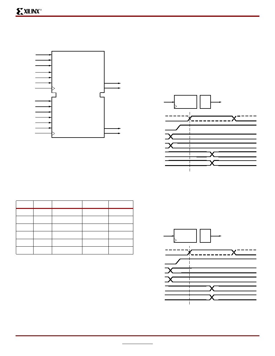
Virtex-II ProTM Platform FPGAs: Functional Description
R
DS083-2 (v2.9) October 14, 2003
www.xilinx.com
35
Advance Product Specification
1-800-255-7778
Each block SelectRAM+ cell is a fully synchronous memory,
as illustrated in
Figure 39
. The two ports have independent
inputs and outputs and are independently clocked.
Port Aspect Ratios
Table 18
shows the depth and the width aspect ratios for the
18 Kb block SelectRAM+ resource. Virtex-II Pro block
SelectRAM+ also includes dedicated routing resources to
provide an efficient interface with CLBs, block SelectRAM+,
and multipliers.
Read/Write Operations
The Virtex-II Pro block SelectRAM+ read operation is fully
synchronous. An address is presented, and the read opera-
tion is enabled by control signal ENA or ENB. Then,
depending on clock polarity, a rising or falling clock edge
causes the stored data to be loaded into output registers.
The write operation is also fully synchronous. Data and
address are presented, and the write operation is enabled
by control signals WEA and WEB in addition to ENA or
ENB. Then, again depending on the clock input mode, a ris-
ing or falling clock edge causes the data to be loaded into
the memory cell addressed.
A write operation performs a simultaneous read operation.
Three different options are available, selected by configura-
tion:
1.
WRITE_FIRST
The WRITE_FIRST option is a transparent mode. The
same clock edge that writes the data input (DI) into the
memory also transfers DI into the output registers DO,
as shown in
Figure 40
.
2.
READ_FIRST
The READ_FIRST option is a read-before-write mode.
The same clock edge that writes data input (DI) into the
memory also transfers the prior content of the memory cell
addressed into the data output registers DO, as shown in
Figure 41
.
Figure 39: 18 Kb Block SelectRAM+ in Dual-Port Mode
Table 18: 18 Kb Block SelectRAM+ Port Aspect Ratio
Width
Depth
Address Bus
Data Bus
Parity Bus
1
16,384
ADDR[13:0]
DATA[0]
N/A
2
8,192
ADDR[12:0]
DATA[1:0]
N/A
4
4,096
ADDR[11:0]
DATA[3:0]
N/A
9
2,048
ADDR[10:0]
DATA[7:0] Parity[0]
18
1,024
ADDR[9:0]
DATA[15:0] Parity[1:0]
36
512
ADDR[8:0]
DATA[31:0]
Parity[3:0]
DOPA
DOPB
DIPA
ADDRA
WEA
ENA
SSRA
CLKA
DIPB
ADDRB
WEB
ENB
SSRB
CLKB
18-Kbit Block SelectRAM
DS031_11_102000
DOB
DOA
DIA
DIB
Figure 40: WRITE_FIRST Mode
Figure 41: READ_FIRST Mode
CLK
WE
Data_in
Data_in
New
aa
Address
Internal
Memory
DO
Data_out = Data_in
Data_out
DI
DS083-2_14_050901
New
RAM Contents
New
Old
CLK
WE
Data_in
Data_in
New
aa
Old
Address
Internal
Memory
DO
Prior stored data
Data_out
DI
DS083-2_13_050901
RAM Contents
New
Old
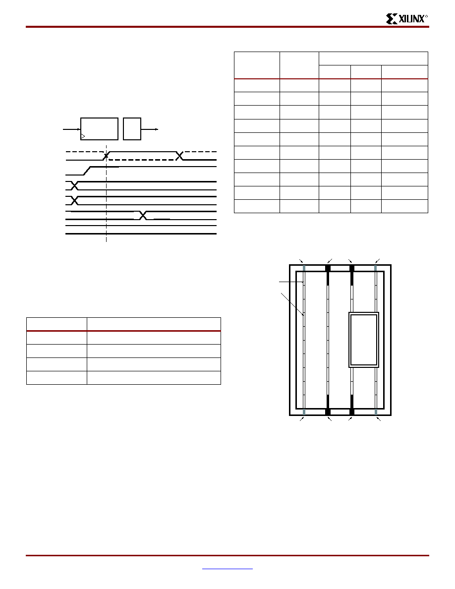
Functional Description: FPGA
R
36
www.xilinx.com
DS083-2 (v2.9) October 14, 2003
1-800-255-7778
Advance Product Specification
3.
NO_CHANGE
The NO_CHANGE option maintains the content of the out-
put registers, regardless of the write operation. The clock
edge during the write mode has no effect on the content of
the data output register DO. When the port is configured as
NO_CHANGE, only a read operation loads a new value in
the output register DO, as shown in
Figure 42
.
Control Pins and Attributes
Virtex-II Pro SelectRAM+ memory has two independent
ports with the control signals described in
Table 19
. All con-
trol inputs including the clock have an optional inversion.
Initial memory content is determined by the INIT_xx
attributes. Separate attributes determine the output register
value after device configuration (INIT) and SSR is asserted
(SRVAL). Both attributes (INIT_B and SRVAL) are available
for each port when a block SelectRAM+ resource is config-
ured as dual-port RAM.
Total Amount of SelectRAM+ Memory
Virtex-II Pro SelectRAM+ memory blocks are organized in
multiple columns. The number of blocks per column
depends on the row size, the number of Processor Blocks,
and the number of RocketIO transceivers.
Table 20
shows the number of columns as well as the total
amount of block SelectRAM+ memory available for each
Virtex-II Pro device. The 18 Kb SelectRAM+ blocks are
cascadable to implement deeper or wider single- or dual-port
memory resources.
Figure 43
shows the layout of the block RAM columns in the
XC2VP4 device.
18-Bit x 18-Bit Multipliers
Introduction
A Virtex-II Pro multiplier block is an 18-bit by 18-bit 2's com-
plement signed multiplier. Virtex-II Pro devices incorporate
many embedded multiplier blocks. These multipliers can be
associated with an 18 Kb block SelectRAM+ resource or
can be used independently. They are optimized for
high-speed operations and have a lower power consump-
tion compared to an 18-bit x 18-bit multiplier in slices.
Figure 42: NO_CHANGE Mode
Table 19: Control Functions
Control Signal
Function
CLK
Read and Write Clock
EN
Enable affects Read, Write, Set, Reset
WE
Write Enable
SSR
Set DO register to SRVAL (attribute)
CLK
WE
Data_in
Data_in
New
aa
Last Read Cycle Content (no change)
Address
Internal
Memory
DO
No change during write
Data_out
DI
DS083-2_12_050901
RAM Contents
New
Old
Table 20: Virtex-II Pro SelectRAM+ Memory Available
Device
Columns
Total SelectRAM+ Memory
Blocks
in Kb
in Bits
XC2VP2
4
12
216
221,184
XC2VP4
4
28
504
516,096
XC2VP7
6
44
792
811,008
XC2VP20
8
88
1,584
1,622,016
XC2VP30
8
136
2,448
2,506,752
XC2VP40
10
192
3,456
3,538,944
XC2VP50
12
232
4,176
4,276,224
XC2VP70
14
328
5,904
6,045,696
XC2VP100
16
444
7,992
8,183,808
XC2VP125
18
556
10,008
10,248,192
Figure 43: XC2VP4 Block RAM Column Layout
BRAM
Multiplier
Blocks
PPC405
CPU
CLBs
CLBs
CLBs
CLBs
CLBs
DS083-2_11_010802
TM
RocketIO
Serial Transceivers
TM
RocketIO
Serial Transceivers
DCM
DCM
DCM
DCM
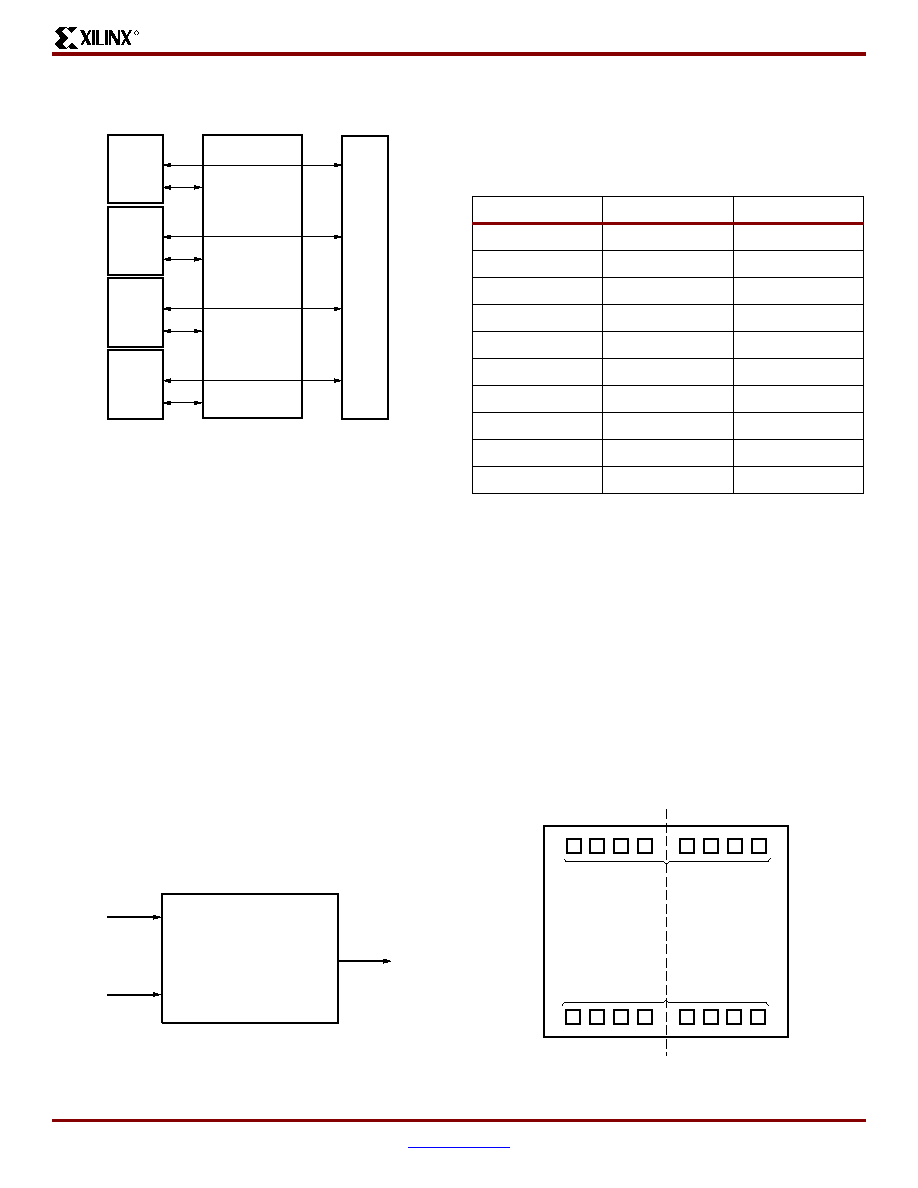
Virtex-II ProTM Platform FPGAs: Functional Description
R
DS083-2 (v2.9) October 14, 2003
www.xilinx.com
37
Advance Product Specification
1-800-255-7778
Each SelectRAM+ memory and multiplier block is tied to
four switch matrices, as shown in
Figure 44
.
Association With Block SelectRAM+ Memory
The interconnect is designed to allow SelectRAM+ memory
and multiplier blocks to be used at the same time, but some
interconnect is shared between the SelectRAM+ and the
multiplier. Thus, SelectRAM+ memory can be used only up
to 18 bits wide when the multiplier is used, because the mul-
tiplier shares inputs with the upper data bits of the
SelectRAM+ memory.
This sharing of the interconnect is optimized for an
18-bit-wide block SelectRAM+ resource feeding the multi-
plier. The use of SelectRAM+ memory and the multiplier
with an accumulator in LUTs allows for implementation of a
digital signal processor (DSP) multiplier-accumulator (MAC)
function, which is commonly used in finite and infinite
impulse response (FIR and IIR) digital filters.
Configuration
The multiplier block is an 18-bit by 18-bit signed multiplier
(2's complement). Both A and B are 18-bit-wide inputs, and
the output is 36 bits.
Figure 45
shows a multiplier block.
Locations / Organization
Multiplier organization is identical to the 18 Kb SelectRAM+
organization, because each multiplier is associated with an
18 Kb block SelectRAM+ resource.
In addition to the built-in multiplier blocks, the CLB elements
have dedicated logic to implement efficient multipliers in
logic. (Refer to
Configurable Logic Blocks (CLBs), page 24
).
Global Clock Multiplexer Buffers
Virtex-II Pro devices have 16 clock input pins that can also
be used as regular user I/Os. Eight clock pads center on
both the top edge and the bottom edge of the device, as
illustrated in
Figure 46
.
The global clock multiplexer buffer represents the input to
dedicated low-skew clock tree distribution in Virtex-II Pro
devices. Like the clock pads, eight global clock multiplexer
buffers are on the top edge of the device and eight are on
the bottom edge.
Figure 44: SelectRAM+ and Multiplier Blocks
Figure 45: Multiplier Block
Switch
Matrix
Switch
Matrix
18-Kbit block
SelectRAM
18 x 18 Multiplier
Switch
Matrix
Switch
Matrix
DS031_33_101000
MULT 18 x 18
A[17:0]
P[35:0]
B[17:0]
Multiplier Block
DS031_40_100400
Table 21: Multiplier Resources
Device
Columns
Total Multipliers
XC2VP2
4
12
XC2VP4
4
28
XC2VP7
6
44
XC2VP20
8
88
XC2VP30
8
136
XC2VP40
10
192
XC2VP50
12
232
XC2VP70
14
328
XC2VP100
16
444
XC2VP125
18
556
Figure 46: Virtex-II Pro Clock Pads
8 clock pads
8 clock pads
Virtex-II Pro
Device
DS083-2_42_052902

Functional Description: FPGA
R
38
www.xilinx.com
DS083-2 (v2.9) October 14, 2003
1-800-255-7778
Advance Product Specification
Each global clock multiplexer buffer can be driven either by
the clock pad to distribute a clock directly to the device, or
by the Digital Clock Manager (DCM), discussed in
Digital
Clock Manager (DCM), page 40
. Each global clock multi-
plexer buffer can also be driven by local interconnects. The
DCM has clock output(s) that can be connected to global
clock multiplexer buffer inputs, as shown in
Figure 47
.
Global clock buffers are used to distribute the clock to some
or all synchronous logic elements (such as registers in
CLBs and IOBs, and SelectRAM+ blocks.
Eight global clocks can be used in each quadrant of the
Virtex-II Pro device. Designers should consider the clock
distribution detail of the device prior to pin-locking and floor-
planning. (See the Virtex-II Pro Platform FPGA User
Guide.)
Figure 48
shows clock distribution in Virtex-II Pro devices.
In each quadrant, up to eight clocks are organized in clock
rows. A clock row supports up to 16 CLB rows (eight up and
eight down).
To reduce power consumption, any unused clock branches
remain static.
Figure 47: Virtex-II Pro Clock Multiplexer Buffer Configuration
Clock
Pad
Local
Interconnect
Clock
Pad
Clock
Buffer
Clock Multiplexer
I
O
Clock Distribution
CLKIN
CLKOUT
DCM
DS083-2_43_122001
Figure 48: Virtex-II Pro Clock Distribution
8
8
8
8
NW
NE
SW
SE
DS083-2_45_122001
8 BUFGMUX
8 max
8 BUFGMUX
16 Clocks
NW
NE
SW
SE
8 BUFGMUX
8 BUFGMUX
16 Clocks
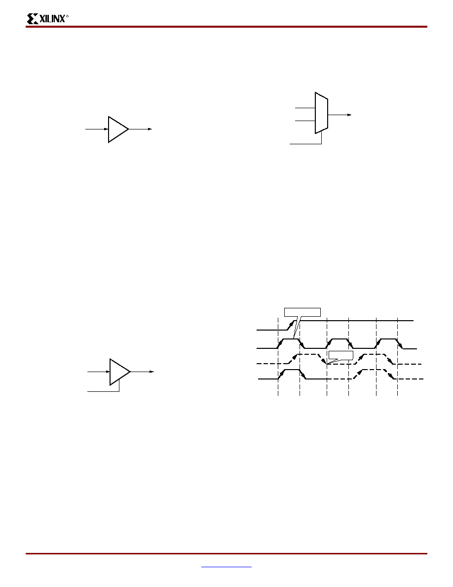
Virtex-II ProTM Platform FPGAs: Functional Description
R
DS083-2 (v2.9) October 14, 2003
www.xilinx.com
39
Advance Product Specification
1-800-255-7778
Global clocks are driven by dedicated clock buffers (BUFG),
which can also be used to gate the clock (BUFGCE) or to mul-
tiplex between two independent clock inputs (BUFGMUX).
The most common configuration option of this element is as
a buffer. A BUFG function in this (global buffer) mode, is
shown in
Figure 49
.
The Virtex-II Pro global clock buffer BUFG can also be con-
figured as a clock enable/disable circuit (
Figure 50
), as well
as a two-input clock multiplexer (
Figure 51
). A functional
description of these two options is provided below. Each of
them can be used in either of two modes, selected by con-
figuration: rising clock edge or falling clock edge.
This section describes the rising clock edge option. For the
opposite option, falling clock edge, just change all "rising"
references to "falling" and all "High" references to "Low",
except for the description of the CE and S levels. The rising
clock edge option uses the BUFGCE and BUFGMUX prim-
itives. The falling clock edge option uses the BUFGCE_1
and BUFGMUX_1 primitives.
BUFGCE
If the CE input is active (High) prior to the incoming rising
clock edge, this Low-to-High-to-Low clock pulse passes
through the clock buffer. Any level change of CE during the
incoming clock High time has no effect.
If the CE input is inactive (Low) prior to the incoming rising
clock edge, the following clock pulse does not pass through
the clock buffer, and the output stays Low. Any level change
of CE during the incoming clock High time has no effect. CE
must not change during a short setup window just prior to
the rising clock edge on the BUFGCE input I. Violating this
setup time requirement can result in an undefined runt
pulse output.
BUFGMUX
BUFGMUX can switch between two unrelated, even asyn-
chronous clocks. Basically, a Low on S selects the I
0
input,
a High on S selects the I
1
input. Switching from one clock to
the other is done in such a way that the output High and Low
time is never shorter than the shortest High or Low time of
either input clock. As long as the presently selected clock is
High, any level change of S has no effect.
If the presently selected clock is Low while S changes, or if
it goes Low after S has changed, the output is kept Low until
the other ("to-be-selected") clock has made a transition
from High to Low. At that instant, the new clock starts driv-
ing the output.
The two clock inputs can be asynchronous with regard to
each other, and the S input can change at any time, except
for a short setup time prior to the rising edge of the presently
selected clock; that is, prior to the rising edge of the
BUFGMUX output O. Violating this setup time requirement
can result in an undefined runt pulse output.
All Virtex-II Pro devices have 16 global clock multiplexer
buffers.
Figure 52
shows a switchover from CLK0 to CLK1.
∑
The current clock is CLK0.
∑
S is activated High.
∑
If CLK0 is currently High, the multiplexer waits for CLK0
to go Low.
∑
Once CLK0 is Low, the multiplexer output stays Low
until CLK1 transitions High to Low.
∑
When CLK1 transitions from High to Low, the output
switches to CLK1.
∑
No glitches or short pulses can appear on the output.
Figure 49: Virtex-II Pro BUFG Function
Figure 50: Virtex-II Pro BUFGCE Function
O
I
BUFG
DS031_61_101200
O
I
CE
BUFGCE
DS031_62_101200
Figure 51: Virtex-II Pro BUFGMUX Function
Figure 52: Clock Multiplexer Waveform Diagram
O
I
0
I
1
S
BUFGMUX
DS083-2_63_121701
S
C L K 0
CLK1
Out
Wait for Low
Switch
DS083-2_46_121701

Functional Description: FPGA
R
40
www.xilinx.com
DS083-2 (v2.9) October 14, 2003
1-800-255-7778
Advance Product Specification
Local Clocking
In addition to global clocks, there are local clock resources
in the Virtex-II Pro devices. There are more than 72 local
clocks in the Virtex-II Pro family. These resources can be
used for many different applications, including but not lim-
ited to memory interfaces. For example, even using only the
left and right I/O banks, Virtex-II Pro FPGAs can support up
to 50 local clocks for DDR SDRAM. These interfaces can
operate beyond 200 MHz on Virtex-II Pro devices.
Digital Clock Manager (DCM)
The Virtex-II Pro DCM offers a wide range of powerful clock
management features.
∑
Clock De-skew: The DCM generates new system
clocks (either internally or externally to the FPGA),
which are phase-aligned to the input clock, thus
eliminating clock distribution delays.
∑
Frequency Synthesis: The DCM generates a wide
range of output clock frequencies, performing very
flexible clock multiplication and division.
∑
Phase Shifting: The DCM provides both coarse phase
shifting and fine-grained phase shifting with dynamic
phase shift control.
The DCM utilizes fully digital delay lines allowing robust
high-precision control of clock phase and frequency. It also
utilizes fully digital feedback systems, operating dynamically
to compensate for temperature and voltage variations dur-
ing operation.
Up to four of the nine DCM clock outputs can drive inputs to
global clock buffers or global clock multiplexer buffers simul-
taneously (see
Figure 53
). All DCM clock outputs can simul-
taneously drive general routing resources, including routes
to output buffers.
The DCM can be configured to delay the completion of the
Virtex-II Pro configuration process until after the DCM has
achieved lock. This guarantees that the chip does not begin
operating until after the system clocks generated by the
DCM have stabilized.
The DCM has the following general control signals:
∑
RST input pin
:
resets the entire DCM
∑
LOCKED output pin: asserted High when all enabled
DCM circuits have locked.
∑
STATUS output pins (active High): shown in
Table 22
.
Clock De-skew
The DCM de-skews the output clocks relative to the input
clock by automatically adjusting a digital delay line. Addi-
tional delay is introduced so that clock edges arrive at inter-
nal registers and block RAMs simultaneously with the clock
edges arriving at the input clock pad. Alternatively, external
clocks, which are also de-skewed relative to the input clock,
can be generated for board-level routing. All DCM output
clocks are phase-aligned to CLK0 and, therefore, are also
phase-aligned to the input clock.
To achieve clock de-skew, the CLKFB input must be con-
nected, and its source must be either CLK0 or CLK2X. Note
that CLKFB must always be connected, unless only the
CLKFX or CLKFX180 outputs are used and de-skew is not
required.
Frequency Synthesis
The DCM provides flexible methods for generating new
clock frequencies. Each method has a different operating
frequency range and different AC characteristics. The
CLK2X and CLK2X180 outputs double the clock frequency.
The CLKDV output creates divided output clocks with divi-
sion options of 1.5, 2, 2.5, 3, 3.5, 4, 4.5, 5, 5.5, 6, 6.5, 7, 7.5,
8, 9, 10, 11, 12, 13, 14, 15, and 16.
The CLKFX and CLKFX180 outputs can be used to pro-
duce clocks at the following frequency:
Figure 53: Digital Clock Manager
CLKIN
CLKFB
CLK180
CLK270
CLK0
CLK90
CLK2X
CLK2X180
CLKDV
DCM
DS031_67_112900
CLKFX
CLKFX180
LOCKED
STATUS[7:0]
PSDONE
RST
DSSEN
PSINCDEC
PSEN
PSCLK
clock signal
control signal
Table 22: DCM Status Pins
Status Pin
Function
0
Phase Shift Overflow
1
CLKIN Stopped
2
CLKFX Stopped
3
N/A
4
N/A
5
N/A
6
N/A
7
N/A
FREQ
CLKFX
M D
/
(
) FREQ
CLKIN
∑
=
Virtex-II ProTM Platform FPGAs: Functional Description
R
DS083-2 (v2.9) October 14, 2003
www.xilinx.com
41
Advance Product Specification
1-800-255-7778
where M and D are two integers. Specifications for M and D
are provided under DCM Timing Parameters in
Data
Sheet Module 3
.
By default, M = 4 and D = 1, which results
in a clock output frequency four times faster than the clock
input frequency (CLKIN).
CLK2X180 is phase shifted 180 degrees relative to CLK2X.
CLKFX180 is phase shifted 180 degrees relative to CLKFX.
All frequency synthesis outputs automatically have 50/50
duty cycles, with the exception of the CLKDV output when
performing a non-integer divide in high-frequency mode.
See
Table 23
for more details.
Note that CLK2X and CLK2X180 are not available in
high-frequency mode.
Phase Shifting
The DCM provides additional control over clock skew
through either coarse or fine-grained phase shifting. The
CLK0, CLK90, CLK180, and CLK270 outputs are each
phase shifted by º of the input clock period relative to each
other, providing coarse phase control. Note that CLK90 and
CLK270 are not available in high-frequency mode.
Fine-phase adjustment affects all nine DCM output clocks.
When activated, the phase shift between the rising edges of
CLKIN and CLKFB is a specified fraction of the input clock
period.
In variable mode, the
PHASE_SHIFT
value can also be
dynamically incremented or decremented as determined by
PSINCDEC synchronously to PSCLK, when the PSEN
input is active.
Figure 54
illustrates the effects of fine-phase
shifting. For more information on DCM features, see the
Virtex-II Pro Platform FPGA User Guide.
Table 24
lists fine-phase shifting control pins, when used in
variable mode.
Two separate components of the phase shift range must be
understood:
∑
PHASE_SHIFT
attribute range
∑
FINE_SHIFT_RANGE
DCM timing parameter range
The
PHASE_SHIFT
attribute is the numerator in the following
equation:
Phase Shift (ns) = (
PHASE_SHIFT
/256) * PERIOD
CLKIN
The full range of this attribute is always -255 to +255, but its
practical range varies with CLKIN frequency, as constrained
by the
FINE_SHIFT_RANGE
component, which represents
the total delay achievable by the phase shift delay line. Total
delay is a function of the number of delay taps used in the
Table 23: CLKDV Duty Cycle for Non-integer Divides
CLKDV_DIVIDE
Duty Cycle
1.5
1/ 3
2.5
2 / 5
3.5
3 / 7
4.5
4 / 9
5.5
5 / 11
6.5
6 / 13
7.5
7 / 15
Table 24: Fine Phase Shifting Control Pins
Control Pin
Direction
Function
PSINCDEC
In
Increment or decrement
PSEN
In
Enable ± phase shift
PSCLK
In
Clock for phase shift
PSDONE
Out
Active when completed
Figure 54: Fine-Phase Shifting Effects
CLKOUT_PHASE_SHIFT
= FIXED
CLKOUT_PHASE_SHIFT
= VARIABLE
CLKOUT_PHASE_SHIFT
= NONE
CLKIN
CLKFB
CLKIN
CLKIN
CLKFB
(PS/256) x PERIODCLKIN
(PS negative)
(PS/256) x PERIODCLKIN
(PS positive)
CLKFB
(PS/256) x PERIODCLKIN
(PS negative)
(PS/256) x PERIODCLKIN
(PS positive)
DS031_48_110300
Functional Description: FPGA
R
42
www.xilinx.com
DS083-2 (v2.9) October 14, 2003
1-800-255-7778
Advance Product Specification
circuit. Across process, voltage, and temperature, this abso-
lute range is guaranteed to be as specified under DCM Tim-
ing Parameters in
Data Sheet Module 3
.
Absolute range (fixed mode) = ±
FINE_SHIFT_RANGE
Absolute range (variable mode) = ±
FINE_SHIFT_RANGE
/2
The reason for the difference between fixed and variable
modes is as follows. For variable mode to allow symmetric,
dynamic sweeps from -255/256 to +255/256, the DCM sets
the "zero phase skew" point as the middle of the delay line,
thus dividing the total delay line range in half. In fixed mode,
since the
PHASE_SHIFT
value never changes after configu-
ration, the entire delay line is available for insertion into
either the CLKIN or CLKFB path (to create either positive or
negative skew).
Taking both of these components into consideration, the fol-
lowing are some usage examples:
∑
If PERIOD
CLKIN
= 2 *
FINE_SHIFT_RANGE
, then
PHASE_SHIFT in
fixed mode is limited to
±
128, and in
variable mode it is limited to
±
64.
∑
If PERIOD
CLKIN
=
FINE_SHIFT_RANGE
, then
PHASE_SHIFT in
fixed mode is limited to
±
255, and in
variable mode it is limited to
±
128.
∑
If PERIOD
CLKIN
0.5 *
FINE_SHIFT_RANGE
, then
PHASE_SHIFT
is limited to
±
255 in either mode.
Operating Modes
The frequency ranges of DCM input and output clocks
depend on the operating mode specified, either
low-frequency mode or high-frequency mode, according to
Table 25
. For actual values, see
Virtex-II Pro Switching
Characteristics (Module 3)
. The CLK2X, CLK2X180,
CLK90, and CLK270 outputs are not available in high-fre-
quency mode.
High or low-frequency mode is selected by an attribute.
Routing
DCM and MGT Locations/Organization
Virtex-II Pro DCMs and serial transceivers (MGTs) are
placed on the top and bottom of each block RAM and multi-
plier column in some combination, as shown in
Table 26
.
The number of DCMs and RocketIO transceivers total twice
the number of block RAM columns in the device. Refer to
Figure 43, page 36
for an illustration of this in the XC2VP4
device.
Place-and-route software takes advantage of this regular
array to deliver optimum system performance and fast com-
pile times. The segmented routing resources are essential
to guarantee IP cores portability and to efficiently handle an
incremental design flow that is based on modular imple-
mentations. Total design time is reduced due to fewer and
shorter design iterations.
Hierarchical Routing Resources
Most Virtex-II Pro signals are routed using the global rout-
ing resources, which are located in horizontal and vertical
routing channels between each switch matrix.
As shown in
Figure 55, page 43
, Virtex-II Pro has fully buff-
ered programmable interconnections, with a number of
resources counted between any two adjacent switch matrix
rows or columns. Fanout has minimal impact on the perfor-
mance of each net.
Table 25: DCM Frequency Ranges
Output Clock
Low-Frequency Mode
High-Frequency Mode
CLKIN Input
CLK Output
CLKIN Input
CLK Output
CLK0, CLK180
CLKIN_FREQ_DLL_LF
CLKOUT_FREQ_1X_LF
CLKIN_FREQ_DLL_HF
CLKOUT_FREQ_1X_HF
CLK90, CLK270
CLKIN_FREQ_DLL_LF
CLKOUT_FREQ_1X_LF
NA
NA
CLK2X, CLK2X180
CLKIN_FREQ_DLL_LF
CLKOUT_FREQ_2X_LF
NA
NA
CLKDV
CLKIN_FREQ_DLL_LF
CLKOUT_FREQ_DV_LF
CLKIN_FREQ_DLL_HF
CLKOUT_FREQ_DV_HF
CLKFX, CLKFX180
CLKIN_FREQ_FX_LF
CLKOUT_FREQ_FX_LF
CLKIN_FREQ_FX_HF
CLKOUT_FREQ_FX_HF
Table 26: DCM Organization
Device
Block RAM
Columns
DCMs
MGTs
XC2VP2
4
4
4
XC2VP4
4
4
4
XC2VP7
6
4
8
XC2VP20
8
8
8
XC2VP30
8
8
8
XC2VP40
10
8
12
XC2VP50
12
8
16
XC2VP70
14
8
20
XC2VP100
16
12
20
XC2VP125
18
12
24
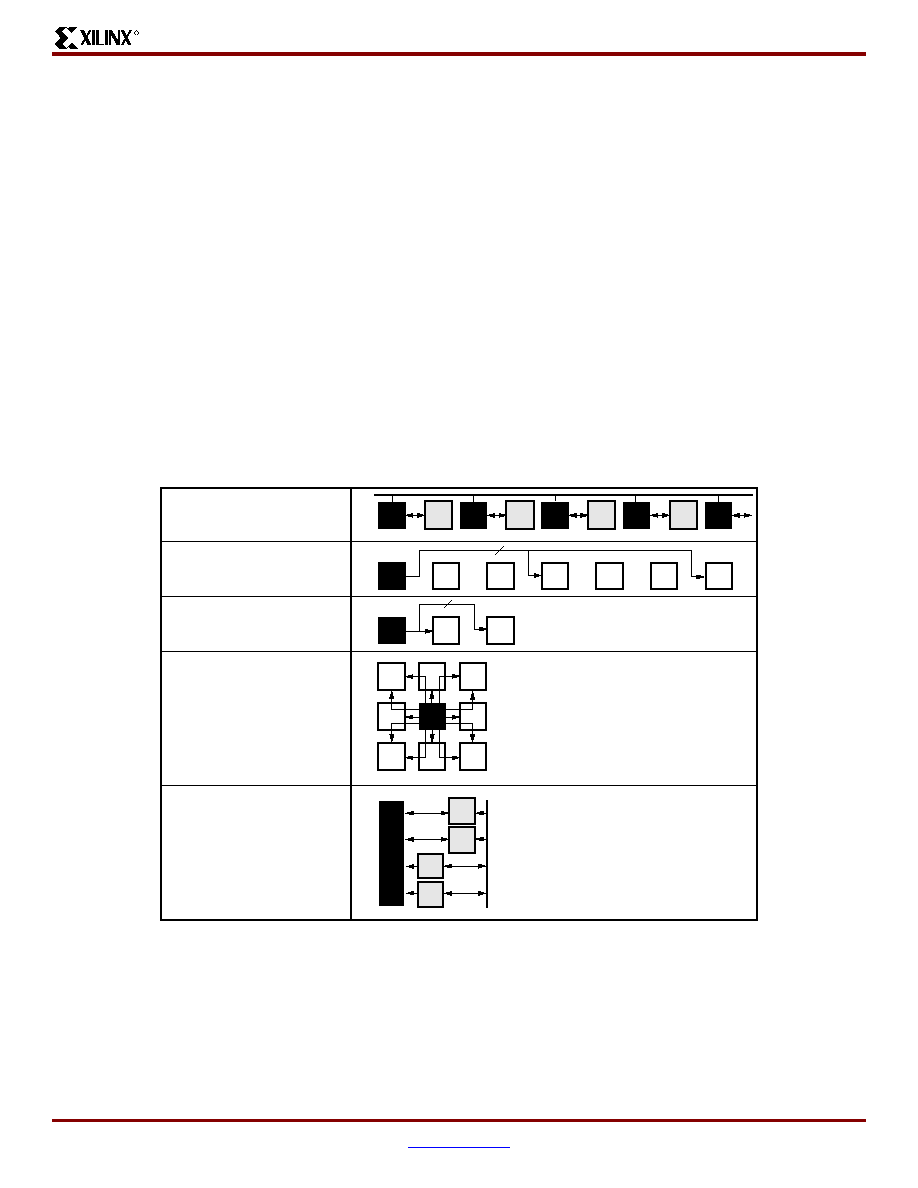
Virtex-II ProTM Platform FPGAs: Functional Description
R
DS083-2 (v2.9) October 14, 2003
www.xilinx.com
43
Advance Product Specification
1-800-255-7778
∑
The long lines are bidirectional wires that distribute
signals across the device. Vertical and horizontal long
lines span the full height and width of the device.
∑
The hex lines route signals to every third or sixth block
away in all four directions. Organized in a staggered
pattern, hex lines can only be driven from one end.
Hex-line signals can be accessed either at the
endpoints or at the midpoint (three blocks from the
source).
∑
The double lines route signals to every first or second
block away in all four directions. Organized in a
staggered pattern, double lines can be driven only at
their endpoints. Double-line signals can be accessed
either at the endpoints or at the midpoint (one block
from the source).
∑
The direct connect lines route signals to neighboring
blocks: vertically, horizontally, and diagonally.
∑
The fast connect lines are the internal CLB local
interconnections from LUT outputs to LUT inputs.
Dedicated Routing
In addition to the global and local routing resources, dedi-
cated signals are available.
∑
There are eight global clock nets per quadrant. (See
Global Clock Multiplexer Buffers, page 37
.)
∑
Horizontal routing resources are provided for on-chip
3-state buses. Four partitionable bus lines are provided
per CLB row, permitting multiple buses within a row.
(See
3-State Buffers, page 32
.)
∑
Two dedicated carry-chain resources per slice column
(two per CLB column) propagate carry-chain MUXCY
output signals vertically to the adjacent slice. (See
CLB/Slice Configurations, page 32
.)
∑
One dedicated SOP chain per slice row (two per CLB
row) propagate ORCY output logic signals horizontally
to the adjacent slice. (See
Sum of Products, page 31
.)
∑
One dedicated shift-chain per CLB connects the output
of LUTs in shift-register mode to the input of the next
LUT in shift-register mode (vertically) inside the CLB.
(See
Shift Registers, page 28
.)
∑
Configuration
Virtex-II Pro devices are configured by loading application
specific configuration data into the internal configuration
memory. Configuration is carried out using a subset of the
device pins, some of which are dedicated, while others can
be re-used as general purpose inputs and outputs once
configuration is complete.
Depending on the system design, several configuration
modes are supported, selectable via mode pins. The mode
pins M2, M1, and M0 are dedicated pins. The M2, M1, and
M0 mode pins should be set at a constant DC voltage level,
Figure 55: Hierarchical Routing Resources
24 Horizontal Long Lines
24 Vertical Long Lines
120 Horizontal Hex Lines
120 Vertical Hex Lines
40 Horizontal Double Lines
40 Vertical Double Lines
16 Direct Connections
(total in all four directions)
8 Fast Connects
DS031_60_110200

Functional Description: FPGA
R
44
www.xilinx.com
DS083-2 (v2.9) October 14, 2003
1-800-255-7778
Advance Product Specification
either through pullup or pulldown resistors, or tied directly to
ground or V
CCAUX
. The mode pins should not be toggled
during and after configuration.
An additional pin, HSWAP_EN is used in conjunction with
the mode pins to select whether user I/O pins have pull-ups
during configuration. By default, HSWAP_EN is tied High
(internal pull-up) which shuts off the pull-ups on the user I/O
pins during configuration. When HSWAP_EN is tied Low,
user I/Os have pull-ups during configuration. Other dedi-
cated pins are CCLK (the configuration clock pin), DONE,
PROG_B, and the boundary-scan pins: TDI, TDO, TMS,
and TCK. (The TDO pin is open-drain and does not have an
internal pullup resistor.) Depending on the configuration
mode chosen, CCLK can be an output generated by the
FPGA, or an input accepting an externally generated clock.
The configuration pins and boundary scan pins are inde-
pendent of the V
CCO
. The auxiliary power supply (V
CCAUX
)
of 2.5V is used for these pins. All configuration pins are
LVCMOS25 12mA. See
Virtex-II Pro Switching Charac-
teristics (Module 3)
.
Configuration Modes
A "persist" option is available which can be used to force the
configuration pins to retain their configuration function even
after device configuration is complete. If the persist option is
not selected then the configuration pins with the exception
of CCLK, PROG_B, and DONE can be used as user I/O in
normal operation. The persist option does not apply to the
boundary-scan related pins. The persist feature is valuable
in applications which employ partial reconfiguration or
reconfiguration on the fly.
Virtex-II Pro supports the following five configuration
modes:
∑
Slave-Serial Mode
∑
Master-Serial Mode
∑
Slave SelectMAP Mode
∑
Master SelectMAP Mode
∑
Boundary-Scan (JTAG, IEEE 1532) Mode
Refer to
Table 27, page 45
.
A detailed description of configuration modes is provided in
the Virtex-II Pro Platform FPGA User Guide.
Slave-Serial Mode
In slave-serial mode, the FPGA receives configuration data
in bit-serial form from a serial PROM or other serial source
of configuration data. The CCLK pin on the FPGA is an
input in this mode. The serial bitstream must be setup at the
DIN input pin a short time before each rising edge of the
externally generated CCLK.
Multiple FPGAs can be daisy-chained for configuration from
a single source. After a particular FPGA has been config-
ured, the data for the next device is routed internally to the
DOUT pin. The data on the DOUT pin changes on the falling
edge of CCLK.
Slave-serial mode is selected by applying [111] to the mode
pins (M2, M1, M0). A weak pull-up on the mode pins makes
slave serial the default mode if the pins are left uncon-
nected.
Master-Serial Mode
In master-serial mode, the CCLK pin is an output pin. It is the
Virtex-II Pro FPGA device that drives the configuration clock
on the CCLK pin to a Xilinx Serial PROM which in turn feeds
bit-serial data to the DIN input. The FPGA accepts this data
on each rising CCLK edge. After the FPGA has been loaded,
the data for the next device in a daisy-chain is presented on
the DOUT pin after the falling CCLK edge.
The interface is identical to slave serial except that an inter-
nal oscillator is used to generate the configuration clock
(CCLK). A wide range of frequencies can be selected for
CCLK which always starts at a slow default frequency. Con-
figuration bits then switch CCLK to a higher frequency for
the remainder of the configuration.
Slave SelectMAP Mode
The SelectMAP mode is the fastest configuration option.
Byte-wide data is written into the Virtex-II Pro FPGA device
with a BUSY flag controlling the flow of data. An external
data source provides a byte stream, CCLK, an active Low
Chip Select (CS_B) signal and a Write signal (RDWR_B). If
BUSY is asserted (High) by the FPGA, the data must be
held until BUSY goes Low. Data can also be read using the
SelectMAP mode. If RDWR_B is asserted, configuration
data is read out of the FPGA as part of a readback opera-
tion.
After configuration, the pins of the SelectMAP port can be
used as additional user I/O. Alternatively, the port can be
retained to permit high-speed 8-bit readback using the per-
sist option.
Multiple Virtex-II Pro FPGAs can be configured using the
SelectMAP mode, and be made to start-up simultaneously.
To configure multiple devices in this way, wire the individual
CCLK, Data, RDWR_B, and BUSY pins of all the devices in
parallel. The individual devices are loaded separately by
deasserting the CS_B pin of each device in turn and writing
the appropriate data.
Master SelectMAP Mode
This mode is a master version of the SelectMAP mode. The
device is configured byte-wide on a CCLK supplied by the
Virtex-II Pro FPGA device. Timing is similar to the Slave
SerialMAP mode except that CCLK is supplied by the
Virtex-II Pro FPGA.
Boundary-Scan (JTAG, IEEE 1532) Mode
In boundary-scan mode, dedicated pins are used for config-
uring the Virtex-II Pro device. The configuration is done
entirely through the IEEE 1149.1 Test Access Port (TAP).
Virtex-II Pro device configuration using Boundary scan is
compliant with IEEE 1149.1-1993 standard and the new

Virtex-II ProTM Platform FPGAs: Functional Description
R
DS083-2 (v2.9) October 14, 2003
www.xilinx.com
45
Advance Product Specification
1-800-255-7778
IEEE 1532 standard for In-System Configurable (ISC)
devices. The IEEE 1532 standard is backward compliant
with the IEEE 1149.1-1993 TAP and state machine. The
IEEE Standard 1532 for In-System Configurable (ISC)
devices is intended to be programmed, reprogrammed, or
tested on the board via a physical and logical protocol. Con-
figuration through the boundary-scan port is always avail-
able, independent of the mode selection. Selecting the
boundary-scan mode simply turns off the other modes.
Table 28
lists the total number of bits required to configure
each device.
Configuration Sequence
The configuration of Virtex-II Pro devices is a three-phase
process. First, the configuration memory is cleared. Next,
configuration data is loaded into the memory, and finally, the
logic is activated by a start-up process.
Configuration is automatically initiated on power-up unless
it is delayed by the user. The INIT_B pin can be held Low
using an open-drain driver. An open-drain is required since
INIT_B is a bidirectional open-drain pin that is held Low by a
Virtex-II Pro FPGA device while the configuration memory
is being cleared. Extending the time that the pin is Low
causes the configuration sequencer to wait. Thus, configu-
ration is delayed by preventing entry into the phase where
data is loaded.
The configuration process can also be initiated by asserting
the PROG_B pin. The end of the memory-clearing phase is
signaled by the INIT_B pin going High, and the completion
of the entire process is signaled by the DONE pin going
High. The Global Set/Reset (GSR) signal is pulsed after the
last frame of configuration data is written but before the
start-up sequence. The GSR signal resets all flip-flops on
the device.
The default start-up sequence is that one CCLK cycle after
DONE goes High, the global 3-state signal (GTS) is
released. This permits device outputs to turn on as neces-
sary. One CCLK cycle later, the Global Write Enable (GWE)
signal is released. This permits the internal storage ele-
ments to begin changing state in response to the logic and
the user clock.
The relative timing of these events can be changed via con-
figuration options in software. In addition, the GTS and
GWE events can be made dependent on the DONE pins of
multiple devices all going High, forcing the devices to start
synchronously. The sequence can also be paused at any
stage, until lock has been achieved on any or all DCMs, as
well as DCI.
Readback
In this mode, configuration data from the Virtex-II Pro FPGA
device can be read back. Readback is supported only in the
SelectMAP (master and slave) and Boundary Scan mode.
Along with the configuration data, it is possible to read back
the contents of all registers, distributed SelectRAM+, and
block RAM resources. This capability is used for real-time
debugging. For more detailed configuration information, see
the Virtex-II Pro Platform FPGA User Guide.
Table 27: Virtex-II Pro Configuration Mode Pin Settings
Configuration Mode
(1)
M2
M1
M0
CCLK Direction
Data Width
Serial D
OUT
(2)
Master Serial
0
0
0
Out
1
Yes
Slave Serial
1
1
1
In
1
Yes
Master SelectMAP
0
1
1
Out
8
No
Slave SelectMAP
1
1
0
In
8
No
Boundary Scan
1
0
1
N/A
1
No
Notes:
1.
The HSWAP_EN pin controls the pullups. Setting M2, M1, and M0 selects the configuration mode, while the HSWAP_EN pin controls
whether or not the pullups are used.
2.
Daisy chaining is possible only in modes where Serial D
OUT
is used. For example, in SelectMAP modes, the first device does NOT
support daisy chaining of downstream devices.
Table 28: Virtex-II Pro Bitstream Lengths
Device
Number of Configuration
Bits
XC2VP2
1,305,440
XC2VP4
3,006,560
XC2VP7
4,485,472
XC2VP20
8,214,624
XC2VP30
11,589,984
XC2VP40
15,868,256
XC2VP50
19,021,408
XC2VP70
26,099,040
XC2VP100
34,292,832
XC2VP125
43,602,784

Revision History
R
46
www.xilinx.com
DS083-2 (v2.9) October 14, 2003
1-800-255-7778
Advance Product Specification
Bitstream Encryption
Virtex-II Pro devices have an on-chip decryptor using one or
two sets of three keys for triple-key Data Encryption Stan-
dard (DES) operation. Xilinx software tools offer an optional
encryption of the configuration data (bitstream) with a tri-
ple-key DES determined by the designer.
The keys are stored in the FPGA by JTAG instruction and
retained by a battery connected to the V
BATT
pin, when the
device is not powered. Virtex-II Pro devices can be config-
ured with the corresponding encrypted bitstream, using any
of the configuration modes described previously.
A detailed description of how to use bitstream encryption is
provided in the Virtex-II Pro Platform FPGA User Guide.
Your local FAE can also provide specific information on this
feature.
Partial Reconfiguration
Partial reconfiguration of Virtex-II Pro devices can be
accomplished in either Slave SelectMAP mode or Bound-
ary-Scan mode. Instead of resetting the chip and doing a
full configuration, new data is loaded into a specified area of
the chip, while the rest of the chip remains in operation.
Data is loaded on a column basis, with the smallest load unit
being a configuration "frame" of the bitstream (device size
dependent).
Partial reconfiguration is useful for applications that require
different designs to be loaded into the same area of a chip,
or that require the ability to change portions of a design
without having to reset or reconfigure the entire chip.
For more information on Partial Reconfiguration in
Virtex-II Pro devices, please refer to Xilinx Application Note
XAPP290
, Two Flows for Partial Reconfiguration.
Revision History
This section records the change history for this module of the data sheet.
Date
Version
Revision
01/31/02
1.0
Initial Xilinx release.
06/13/02
2.0
New Virtex-II Pro family members. New timing parameters per speedsfile v1.62.
09/03/02
2.1
∑
Revised
Reset
and
Power
sections.
∑
Updated
Table 8
, which lists compatible input standards. [Table deleted in v2.6.]
∑
Added
Figure 19
,
Figure 20
, and
Figure 21
, which provide examples illustrating the
use of I/O standards.
09/27/02
2.2
∑
In section
Overview
, corrected max number of MGTs from 16 to 24.
∑
In section
Input/Output Blocks (IOBs)
, added references to XAPP653 regarding
implementation of 3.3V I/O standards.
11/20/02
2.3
∑
Table 3
: Added rows for LVTTL, LVCMOS33, and PCI-X.
∑
Table 8
: Added LVTTL and LVCMOS33 to compatible 3.3V cells. [Table deleted in v2.6.]
∑
Table 28
: Correct bitstream lengths.
12/03/02
2.4
∑
Added mention of LVTTL and PCI with respect to SelectIO-Ultra configurations. See
section
Input/Output Individual Options
and
Figure 13
.
01/20/03
2.5
∑
Added qualification to features vs. Virtex-II (open-drain output pin TDO does not have
internal pullup resistor)
∑
Table 7: Added HSTL18 (I, II, III, & IV) and HSTL18_DCI (I,II, III & IV) to 1.8V VCCO
row. [Table deleted in v2.6.]
∑
Table 8: Numerous revisions. [Table deleted in v2.6.]
03/24/03
2.5.1
∑
Table 5
: Corrected I/O standard names SSTL18_I and SSTL18_II to SSTL18_I_DCI
and SSTL18_II_DCI respectively.
∑
Figure 52
, text below: Corrected wording of criteria for clock switching.
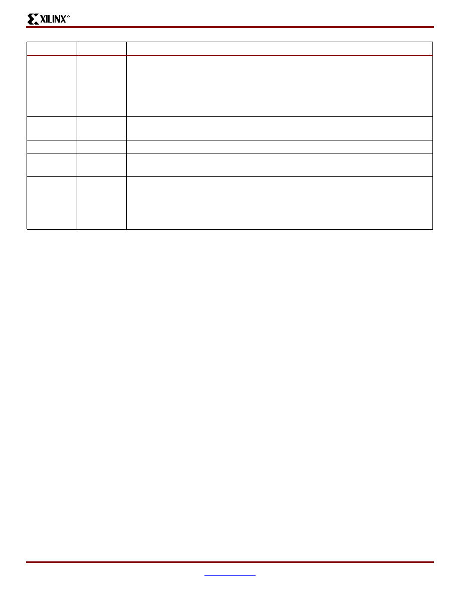
Virtex-II ProTM Platform FPGAs: Functional Description
R
DS083-2 (v2.9) October 14, 2003
www.xilinx.com
47
Advance Product Specification
1-800-255-7778
Virtex-II Pro Data Sheet
The Virtex-II Pro Data Sheet contains the following modules:
∑
Virtex-II ProTM Platform FPGAs: Introduction and
Overview (Module 1)
∑
Virtex-II ProTM Platform FPGAs: Functional Description
(Module 2)
∑
Virtex-II ProTM Platform FPGAs: DC and Switching
Characteristics (Module 3)
∑
Virtex-II ProTM Platform FPGAs: Pinout Information
(Module 4)
05/27/03
2.6
∑
Removed Compatible Output Standards and Compatible Input Standards tables.
∑
Added new
Table 7
,
Summary of Voltage Supply Requirements for All Input and
Output Standards
. This table replaces deleted I/O standards tables.
∑
Corrected sentence in section
Input/Output Individual Options, page 16
, to read "The
optional weak-keeper circuit is connected to each user I/O pad."
∑
Added section
Rules for Combining I/O Standards in the Same Bank, page 18
.
06/02/03
2.7
∑
Added four Differential Termination I/O standards to
Table 4
and
Table 7
.
∑
Added section
On-Chip Differential Termination
and
Figure 22, page 23
.
08/25/03
2.7.1
∑
Added footnote referring to XAPP659 to 3.3V I/O callouts in
Table 3
and
Table 7
.
09/10/03
2.8
∑
Section
Configuration, page 43
: Added text indicating that the mode pins M0-M2 must
be held to a constant DC level during and after configuration.
10/14/03
2.9
∑
Deleted section
Power Sequencing, page 6
. Added section
Local Clocking, page 40
.
∑
Sections
Slave-Serial Mode
and
Master-Serial Mode, page 44
: Changed "rising" to
"falling" edge with respect to DOUT.
∑
Table 3, page 13
and
Table 5, page 14
: Corrected Input V
REF
for HSTL_III-IV_18 from
1.08V to 1.1V.
Date
Version
Revision

Virtex-II Pro Data Sheet
R
48
www.xilinx.com
DS083-2 (v2.9) October 14, 2003
1-800-255-7778
Advance Product Specification
© 2003 Xilinx, Inc. All rights reserved. All Xilinx trademarks, registered trademarks, patents, and disclaimers are as listed at
http://www.xilinx.com/legal.htm
.
All other trademarks and registered trademarks are the property of their respective owners. All specifications are subject to change without notice.
DS083-3 (v2.12) November 11, 2003
www.xilinx.com
1
Advance Product Specification
1-800-255-7778
`6
Virtex-II Pro Electrical Characteristics
Virtex-II Pro devices are provided in -7, -6, and -5 speed
grades, with -7 having the highest performance.
Virtex-II Pro DC and AC characteristics are specified for
both commercial and industrial grades. Except the operat-
ing temperature range or unless otherwise noted, all the DC
and AC electrical parameters are the same for a particular
speed grade (that is, the timing characteristics of a -6 speed
grade industrial device are the same as for a -6 speed grade
commercial device). However, only selected speed grades
and/or devices might be available in the industrial range.
All supply voltage and junction temperature specifications
are representative of worst-case conditions. The parame-
ters included are common to popular designs and typical
applications. Contact Xilinx for design considerations
requiring more detailed information.
All specifications are subject to change without notice.
Virtex-II Pro DC Characteristics
0
54
Virtex-II ProTM Platform FPGAs:
DC and
Switching
Characteristics
DS083-3 (v2.12) November 11, 2003
0
0
Advance Product Specification
R
Table 1: Absolute Maximum Ratings
Symbol
Description
Units
V
CCINT
Internal supply voltage relative to GND
≠0.5 to 1.6
V
V
CCAUX
Auxiliary supply voltage relative to GND
≠0.5 to 3.0
V
V
CCO
Output drivers supply voltage relative to GND
≠0.5 to 3.75
V
V
BATT
Key memory battery backup supply
≠0.5 to 3.0
V
V
REF
Input reference voltage
≠0.3 to 3.75
V
V
IN
3.3V I/O input voltage relative to GND (user and dedicated I/Os)
≠0.3 to 4.05
(3)
V
2.5V or below I/O input voltage relative to GND (user and dedicated I/Os)
≠0.5 to V
CCO
+ 0.5
V
V
TS
Voltage applied to 3-state 3.3V output (user and dedicated I/Os)
≠0.3 to 4.05
(3)
V
Voltage applied to 3-state 2.5V or below output (user and dedicated I/Os)
≠0.5 to V
CCO
+ 0.5
V
V
CCAUXRX
Auxilliary supply voltage relative to analog ground, GNDA (RocketIO pins)
≠0.5 to 3.0
V
V
CCAUXTX
Auxilliary supply voltage relative to analog ground, GNDA (RocketIO pins)
≠0.5 to 3.0
V
V
TTX
Terminal transmit supply voltage relative to GND (RocketIO pins)
≠0.5 to 3.0
V
V
TRX
Terminal receive supply voltage relative to GND (RocketIO pins)
≠0.5 to 3.0
V
T
STG
Storage temperature (ambient)
≠65 to +150
∞C
T
SOL
Maximum soldering temperature
(2)
+220
∞C
T
J
Maximum junction temperature
(2)
+125
∞C
Notes:
1.
Stresses beyond those listed under Absolute Maximum Ratings might cause permanent damage to the device. These are stress
ratings only, and functional operation of the device at these or any other conditions beyond those listed under Operating Conditions
is not implied. Exposure to Absolute Maximum Ratings conditions for extended periods of time might affect device reliability.
2.
For soldering guidelines and thermal considerations, see the
Device Packaging
information on the Xilinx website.
3.
3.3V I/O Absolute Maximum limit applied to DC and AC signals. Refer to
XAPP659
for more details.

R
2
www.xilinx.com
DS083-3 (v2.12) November 11, 2003
1-800-255-7778
Advance Product Specification
Table 2: Recommended Operating Conditions
Symbol
Description
Min
Max
Units
V
CCINT
Internal supply voltage relative to GND, T
J
= 0
∞C to +85∞C
Commercial
1.425
1.575
V
Internal supply voltage relative to GND, T
J
= ≠40
∞C to +100∞C
Industrial
1.425
1.575
V
V
CCAUX
(1)
Auxiliary supply voltage relative to GND, T
J
= 0
∞C to +85∞C
Commercial
2.375
2.625
V
Auxiliary supply voltage relative to GND, T
J
= ≠40
∞C to +100∞C
Industrial
2.375
2.625
V
V
CCO
(2,3)
Supply voltage relative to GND, T
J
= 0
∞C to +85∞C
Commercial
1.2
3.45
(5)
V
Supply voltage relative to GND, T
J
= ≠40
∞C to +100∞C
Industrial
1.2
3.45
(5)
V
V
IN
3.3V supply voltage relative to GND, T
J
= 0
∞C to +85∞C
Commercial
GND ≠ 0.2
3.45
(5)
V
3.3V supply voltage relative to GND, T
J
= ≠40
∞C to +100∞C
Industrial
GND ≠ 0.2
3.45
(5)
V
2.5V and below supply voltage relative to GND, T
J
= 0
∞C to +85∞C
Commercial
GND ≠ 0.2
V
CCO
+ 0.2
V
2.5V and below supply voltage relative to GND, T
J
= ≠40
∞C to +100∞C
Industrial
GND ≠ 0.2
V
CCO
+ 0.2
V
V
BATT
(4)
Battery voltage relative to GND, T
J
= 0
∞C to +85∞C
Commercial
1.0
2.63
V
Battery voltage relative to GND, T
J
= ≠40
∞C to +100∞C
Industrial
1.0
2.63
V
V
CCAUXRX,
(6)
V
CCAUXTX
(6)
Auxilliary supply voltage relative to GNDA
Commercial
2.375
2.625
V
Auxilliary supply voltage relative to GNDA
Industrial
2.375
2.625
V
V
TTX,
V
TRX
Terminal supply voltage relative to GND
Commercial
1.8
2.625
V
Terminal supply voltage relative to GND
Industrial
1.8
2.625
V
Notes:
1.
Recommended maximum voltage droop for V
CCAUX
is 10 mV/ms.
2.
Configuration data is retained even if V
CCO
drops to 0V.
3.
For 3.3V I/O operation, refer to
XAPP659
, available on the Xilinx website at
www.xilinx.com
.
4.
If battery is not used, do not connect V
BATT
.
5.
For PCI and PCI-X, refer to
XAPP653
, available on the Xilinx website at
www.xilinx.com
.
6.
IMPORTANT! All unused RocketIO transceivers in the FPGA must be connected to power and ground. If RocketIO transceivers in the
FPGA are used, refer to the information on power filtering in the
RocketIO Transceiver User Guide
. Unused transceivers can be
powered by any 2.5V source, and passive filtering is not required.
Virtex-II ProTM Platform FPGAs: DC and Switching Characteristics
R
DS083-3 (v2.12) November 11, 2003
www.xilinx.com
3
Advance Product Specification
1-800-255-7778
Table 3: DC Characteristics Over Recommended Operating Conditions
Symbol
Description
Min
Typ
Max
Units
V
DRINT
Data retention V
CCINT
voltage
(below which configuration data might be lost)
1.25
V
V
DRI
Data retention V
CCAUX
voltage
(below which configuration data might be lost)
2.0
V
I
REF
V
REF
current per pin
10
µA
I
L
Input or output leakage current per pin (sample-tested)
10
µA
C
IN
Input capacitance (sample-tested)
10
pF
I
RPU
Pad pull-up (when selected) @ V
in
= 0V, V
CCO
= 2.5V
(sample tested)
150
µA
I
RPD
Pad pull-down (when selected) @ V
in
= 2.5V
(sample-tested)
150
µA
I
BATT
Battery supply current
100
nA
I
CCAUXTX
Operating V
CCAUXTX
supply current
60
mA
I
CCAUXRX
Operating V
CCAUXRX
supply current
35
mA
I
TTX
Operating I
TTX
supply current when transmitter is AC coupled
30
mA
Operating I
TTX
supply current when transmitter is DC coupled
15
mA
I
TRX
Operating I
TRX
supply current when receiver is AC coupled
mA
Operating I
TRX
supply current when receiver is DC coupled
15
mA
P
CPU
Power dissipation of PowerPC
Æ
405 processor block
0.9
mW/MHz
P
RXTX
Power dissipation of RocketIO @ 3.125 Gb/s per channel
350
mW
Power dissipation of RocketIO @ 2.5 Gb/s per channel
310
mW
Power dissipation of RocketIO @ 1.25 Gb/s per channel
230
mW

R
4
www.xilinx.com
DS083-3 (v2.12) November 11, 2003
1-800-255-7778
Advance Product Specification
Table 4: Quiescent Supply Current
Symbol
Description
Device
Typ
Max
Units
I
CCINTQ
Quiescent V
CCINT
supply current
XC2VP2
100
300
mA
XC2VP4
150
400
mA
XC2VP7
175
500
mA
XC2VP20
200
600
mA
XC2VP30
250
800
mA
XC2VP40
300
1050
mA
XC2VP50
350
1250
mA
XC2VP70
425
1700
mA
XC2VP100
TBD
TBD
mA
XC2VP125
TBD
TBD
mA
I
CCOQ
Quiescent V
CCO
supply current
XC2VP2
2
8
mA
XC2VP4
2
8
mA
XC2VP7
2
8
mA
XC2VP20
2.5
10
mA
XC2VP30
2.5
10
mA
XC2VP40
2.5
10
mA
XC2VP50
3
12
mA
XC2VP70
3
12
mA
XC2VP100
TBD
TBD
mA
XC2VP125
TBD
TBD
mA
I
CCAUXQ
Quiescent V
CCAUX
supply current
XC2VP2
10
50
mA
XC2VP4
10
50
mA
XC2VP7
10
50
mA
XC2VP20
15
75
mA
XC2VP30
15
75
mA
XC2VP40
15
75
mA
XC2VP50
20
100
mA
XC2VP70
20
100
mA
XC2VP100
TBD
TBD
mA
XC2VP125
TBD
TBD
mA
Notes:
1.
Quiescent current parameter values are specified for Commercial Grade. For Industrial Grade values, multiply Commercial Grade
values by 1.5.
2.
With no output current loads, no active input pull-up resistors, all I/O pins are 3-state and floating.
3.
If DCI or differential signaling is used, more accurate quiescent current estimates can be obtained by using the Power Estimator or
XPOWERTM.
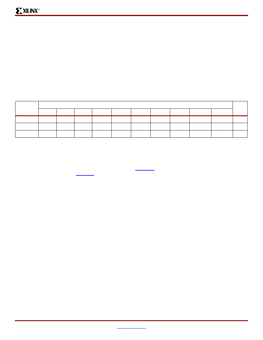
Virtex-II ProTM Platform FPGAs: DC and Switching Characteristics
R
DS083-3 (v2.12) November 11, 2003
www.xilinx.com
5
Advance Product Specification
1-800-255-7778
Power-On Power Supply Requirements
Xilinx FPGAs require a certain amount of supply current
during power-on to insure proper device initialization. The
actual current consumed depends on the power-on ramp
rate of the power supply.
The V
CCINT
power supply must ramp on no faster than
200
µs and no slower than 50 ms. Ramp-on is defined as:
0 V
DC
to minimum supply voltages (see
Table 2
).
V
CCAUX
and V
CCO
can power on at any ramp rate. Power
supplies can be turned on in any sequence, though V
CCAUX
must power on before or with V
CCO
for the specifications
shown in
Table 5
to apply.
Table 5
shows the minimum current required by Virtex-II Pro
devices for proper power-on and configuration.
If the current minimums shown in
Table 5
are met, the
device powers on properly after all three supplies have
passed through their power-on reset threshold voltages.
Once initialized and configured, use the power calculator to
estimate current drain on these supplies.
For more information on V
CCAUX
, V
CCO
, and configuration
mode, refer to Chapter 3 in the Virtex-II Pro Platform FPGA
User Guide.
General Power Supply Requirements
Proper decoupling of all FPGA power supplies is essential.
Consult Xilinx Application Note
XAPP623
for detailed infor-
mation on power distribution system design.
V
CCAUX
powers critical resources in the FPGA. Therefore,
this supply voltage is especially susceptible to power supply
noise. V
CCAUX
can share a power plane with V
CCO
, but only
if V
CCO
does not have excessive noise. Staying within
simultaneously switching output (SSO) limits is essential for
keeping power supply noise to a minimum. Refer to
XAPP689
, "Managing Ground Bounce in Large FPGAs," to
determine the number of simultaneously switching outputs
allowed per bank at the package level.
Changes in V
CCAUX
voltage beyond 200 mV peak-to-peak
should take place at a rate no faster than 10 mV per milli-
second.
Recommended practices that can help reduce jitter and
period distortion are described in Xilinx Answer Record
13756.
Table 5: Power-On Current for Virtex-II Pro Devices
Symbol
Device
Units
XC2VP2
XC2VP4
XC2VP7
XC2VP20
XC2VP30
XC2VP40
XC2VP50
XC2VP70
XC2VP100
XC2VP125
I
CCINTMIN
500
500
500
600
800
1050
1250
1700
TBD
TBD
mA
I
CCAUXMIN
250
250
250
250
250
250
250
250
250
250
mA
I
CCOMIN
100
100
100
100
100
100
100
100
100
100
mA
Notes:
1.
Power-on current parameter values are specified for Commercial Grade. For Industrial Grade values, multiply Commercial Grade
values by 1.5.
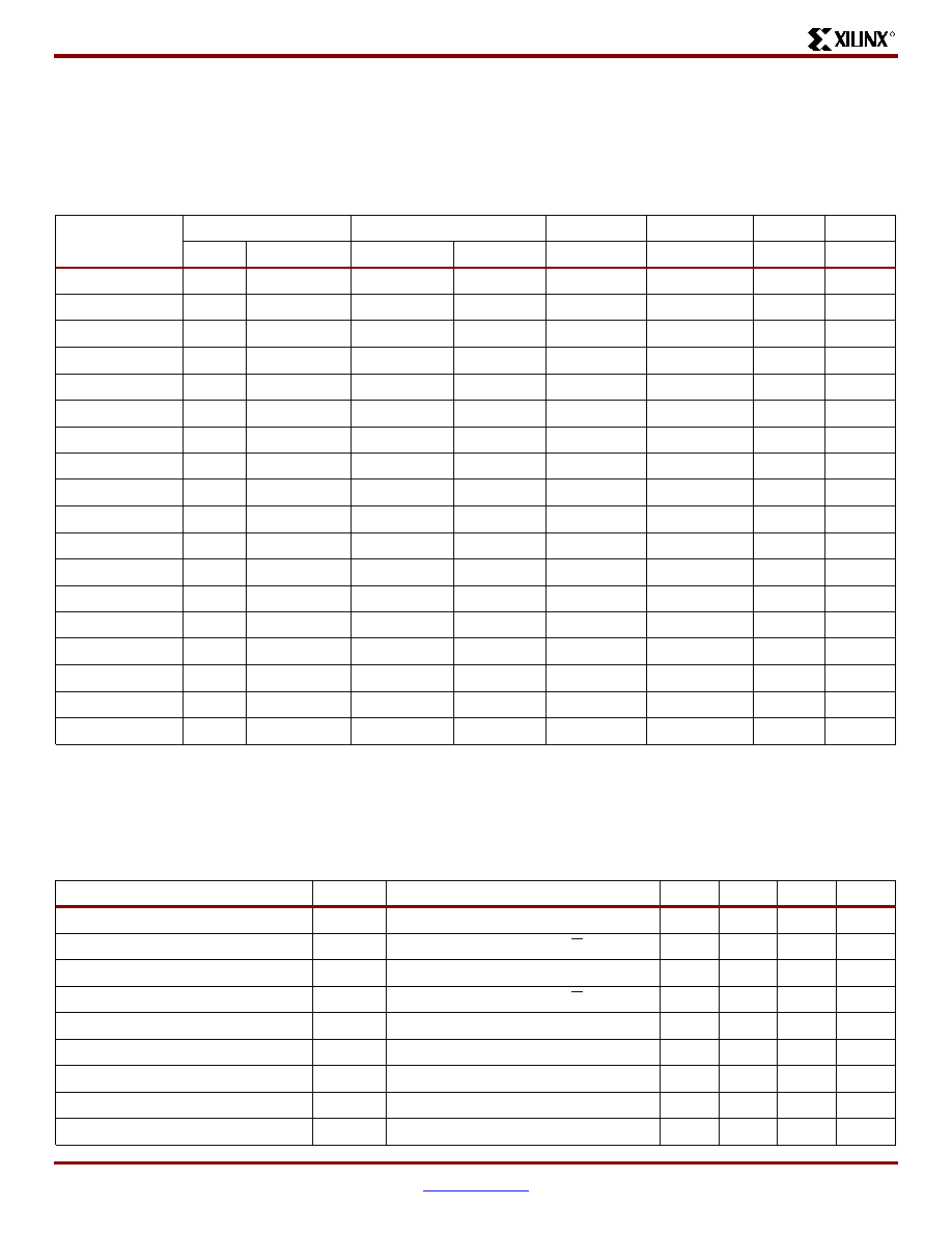
R
6
www.xilinx.com
DS083-3 (v2.12) November 11, 2003
1-800-255-7778
Advance Product Specification
SelectIO-Ultra DC Input and Output Levels
Values for V
IL
and V
IH
are recommended input voltages.
Values for I
OL
and I
OH
are guaranteed over the recom-
mended operating conditions at the V
OL
and V
OH
test
points. Only selected standards are tested. These are cho-
sen to ensure that all standards meet their specifications.
The selected standards are tested at minimum V
CCO
with
the respective V
OL
and V
OH
voltage levels shown. Other
standards are sample tested.
LDT DC Specifications (LDT_25)
Table 6: DC Input and Output Levels
Input/Output
Standard
V
IL
V
IH
V
OL
V
OH
I
OL
I
OH
V, min
V, max
V, min
V, max
V, max
V, min
mA
mA
LVTTL
≠0.2
0.8
2.0
3.45
0.4
2.4
24
≠24
LVCMOS33
≠0.2
0.8
2.0
3.45
0.4
V
CCO
≠ 0.4
24
≠24
LVCMOS25
≠0.2
0.7
1.7
V
CCO
+ 0.4
0.4
V
CCO
≠ 0.4
24
≠24
LVCMOS18
≠0.2
30% V
CCO
70% V
CCO
V
CCO
+ 0.4
0.4
V
CCO
≠ 0.45
16
≠16
LVCMOS15
≠0.2
30% V
CCO
70% V
CCO
V
CCO
+ 0.4
0.4
V
CCO
≠ 0.45
16
≠16
PCI33_3
≠0.2
30% V
CCO
50% V
CCO
3.6
10% V
CCO
90% V
CCO
PCI66_3
≠0.2
30% V
CCO
50% V
CCO
3.6
10% V
CCO
90% V
CCO
PCI-X
≠0.2
Note (1)
Note (1)
Note (1)
Note (1)
Note (1)
Note (1)
Note (1)
GTLP
≠0.2
V
REF
≠ 0.1
V
REF
+ 0.1
V
CCO
+ 0.4
0.6
n/a
36
n/a
GTL
≠0.2
V
REF
≠ 0.05
V
REF
+ 0.05
V
CCO
+ 0.4
0.4
n/a
40
n/a
HSTL I
≠0.2
V
REF
≠ 0.1
V
REF
+ 0.1
V
CCO
+ 0.4
0.4
(2)
V
CCO
≠ 0.4
8
(2)
≠8
(2)
HSTL II
≠0.2
V
REF
≠ 0.1
V
REF
+ 0.1
V
CCO
+ 0.4
0.4
(2)
V
CCO
≠ 0.4
16
(2)
≠16
(2)
HSTL III
≠0.2
V
REF
≠ 0.1
V
REF
+ 0.1
V
CCO
+ 0.4
0.4
(2)
V
CCO
≠ 0.4
24
(2)
≠8
(2)
HSTL IV
≠0.2
V
REF
≠ 0.1
V
REF
+ 0.1
V
CCO
+ 0.4
0.4
(2)
V
CCO
≠ 0.4
48
(2)
≠8
(2)
SSTL2 I
≠0.2
V
REF
≠ 0.15
V
REF
+ 0.15
V
CCO
+ 0.3
V
TT
≠ 0.61
V
TT
+ 0.61
8.1
≠8.1
SSTL2 II
≠0.2
V
REF
≠ 0.15
V
REF
+ 0.15
V
CCO
+ 0.3
V
TT
≠ 0.81
V
TT
+ 0.81
16.2
≠16.2
SSTL18 I
≠0.2
V
REF
≠ 0.125
V
REF
+ 0.125
V
CCO
+ 0.3
V
TT
≠ 0.61
V
TT
+ 0.61
6.7
≠6.7
SSTL18 II
≠0.2
V
REF
≠ 0.125
V
REF
+ 0.125
V
CCO
+ 0.3
V
TT
≠ 0.61
V
TT
+ 0.61
13.4
≠13.4
Notes:
1.
Tested according to relevant specifications.
2.
This applies to 1.5V and 1.8V HSTL.
Table 7: LDT DC Specifications
DC Parameter
Symbol
Conditions
Min
Typ
Max
Units
Supply Voltage
V
CCO
2.38
2.5
2.63
V
Differential Output Voltage
V
OD
R
T
= 100 ohm across Q and Q signals
495
600
715
mV
Change in V
OD
Magnitude
V
OD
≠15
15
mV
Output Common Mode Voltage
V
OCM
R
T
= 100 ohm across Q and Q signals
495
600
715
mV
Change in V
OS
Magnitude
V
OCM
≠15
15
mV
Input Differential Voltage
V
ID
200
600
1000
mV
Change in V
ID
Magnitude
V
ID
≠15
15
mV
Input Common Mode Voltage
V
ICM
440
600
780
mV
Change in V
ICM
Magnitude
V
ICM
≠15
15
mV
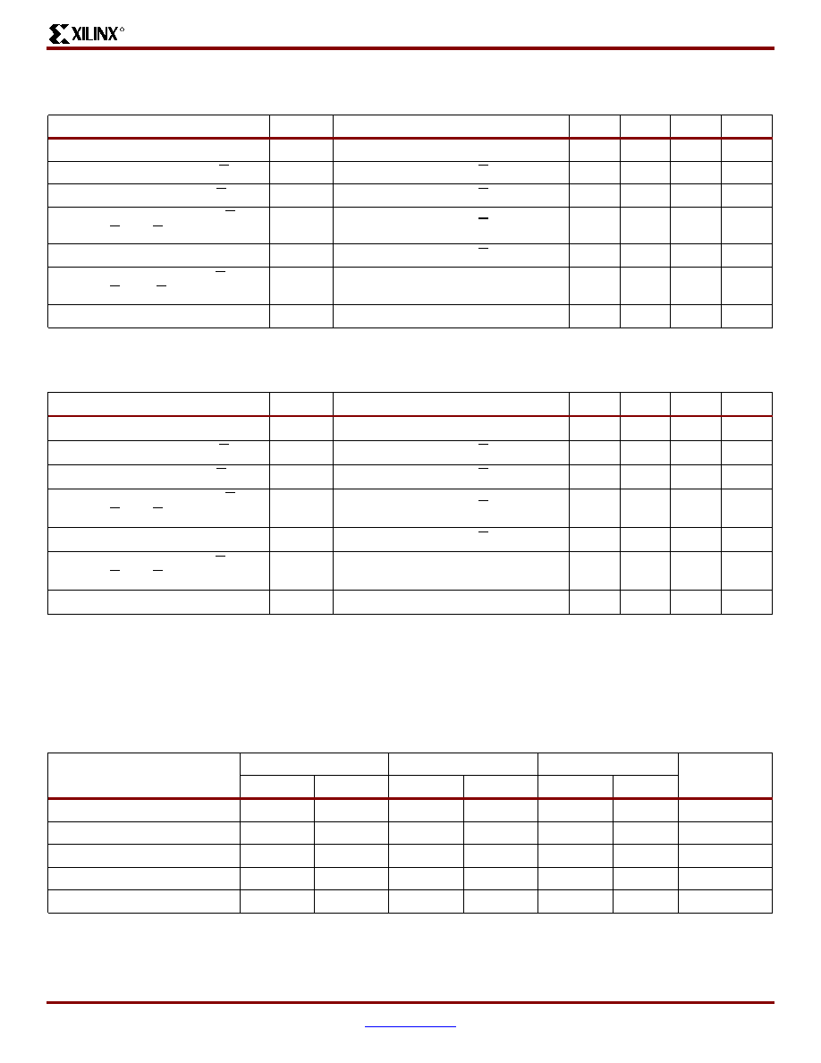
Virtex-II ProTM Platform FPGAs: DC and Switching Characteristics
R
DS083-3 (v2.12) November 11, 2003
www.xilinx.com
7
Advance Product Specification
1-800-255-7778
LVDS DC Specifications (LVDS_25)
Extended LVDS DC Specifications
(LVDSEXT_25)
LVPECL DC Specifications
(LVPECL_25)
These values are valid when driving a 100
differential
load only, i.e., a 100
resistor between the two receiver
pins. The V
OH
levels are 200 mV below standard LVPECL
levels and are compatible with devices tolerant of lower
common-mode ranges.
Table 10
summarizes the DC output
specifications of LVPECL. For more information on using
LVPECL
,
see the Virtex-II Pro Platform FPGA User Guide.
Table 8: LVDS DC Specifications
DC Parameter
Symbol
Conditions
Min
Typ
Max
Units
Supply Voltage
V
CCO
2.38
2.5
2.63
V
Output High Voltage for Q and Q
V
OH
R
T
= 100
across Q and Q signals
1.602
V
Output Low Voltage for Q and Q
V
OL
R
T
= 100
across Q and Q signals
0.898
V
Differential Output Voltage (Q ≠ Q),
Q = High (Q ≠ Q), Q = High
V
ODIFF
R
T
= 100
across Q and Q signals
247
350
454
mV
Output Common-Mode Voltage
V
OCM
R
T
= 100
across Q and Q signals
1.125
1.250
1.375
V
Differential Input Voltage (Q ≠ Q),
Q = High (Q ≠ Q), Q = High
V
IDIFF
Common-mode input voltage = 1.25V
100
350
600
mV
Input Common-Mode Voltage
V
ICM
Differential input voltage =
±350 mV
0.3
1.2
2.2
V
Table 9: Extended LVDS DC Specifications
DC Parameter
Symbol
Conditions
Min
Typ
Max
Units
Supply Voltage
V
CCO
2.38
2.5
2.63
V
Output High Voltage for Q and Q
V
OH
R
T
= 100
across Q and Q signals
1.785
V
Output Low Voltage for Q and Q
V
OL
R
T
= 100
across Q and Q signals
0.715
V
Differential Output Voltage (Q ≠ Q),
Q = High (Q ≠ Q), Q = High
V
ODIFF
R
T
= 100
across Q and Q signals
440
820
mV
Output Common-Mode Voltage
V
OCM
R
T
= 100
across Q and Q signals
1.125
1.250
1.375
V
Differential Input Voltage (Q ≠ Q),
Q = High (Q ≠ Q), Q = High
V
IDIFF
Common-mode input voltage = 1.25V
100
1000
mV
Input Common-Mode Voltage
V
ICM
Differential input voltage =
±350 mV
0.3
1.2
2.2
V
Table 10: LVPECL DC Specifications
DC Parameter
V
CCO
= 2.375V
V
CCO
= 2.5V
V
CCO
= 2.625V
Units
Min
Max
Min
Max
Min
Max
V
OH
1.35
1.495
1.475
1.62
1.6
1.745
V
V
OL
0.565
0.755
0.69
0.88
0.815
1.005
V
V
IH
0.8
2.0
0.8
2.0
0.8
2.0
V
V
IL
0.5
1.7
0.5
1.7
0.5
1.7
V
Differential Input Voltage
0.100
-
0.100
-
0.100
-
V

R
8
www.xilinx.com
DS083-3 (v2.12) November 11, 2003
1-800-255-7778
Advance Product Specification
RocketIO DC Input and Output Levels
Table 11: RocketIO DC Specifications
DC Parameter
Symbol
Conditions
Min
Typ
Max
Units
Peak-to-Peak Differential Input Voltage
DV
IN
175
2000
mV
Single-Ended Output Voltage Swing
(1,2)
DV
OUT
400
mV
500
mV
600
mV
700
mV
800
mV
Peak-to-Peak Differential Output Voltage
(1,2)
DV
PPOUT
800
mV
1000
mV
1200
mV
1400
mV
1600
mV
Notes:
1.
Output swing levels are selectable using TX_DIFF_CTRL attribute. Refer to the RocketIO Transceiver User Guide for details.
2.
Output preemphasis levels are selectable at 10% (default), 20%, 25%, and 33% using the TX_PREEMPHASIS attribute. Refer to the
RocketIO Transceiver User Guide or Chapter 2 in the Virtex-II Pro Platform FPGA User Guide for details.
Figure 1: Single-Ended Output Voltage Swing
0
+V
TXP
TXN
DV
OUT
DS083-3_04_120302
Figure 2: Peak-to-Peak Differential Output Voltage
0
+V
≠V
TXP≠TXN
DV
PPOUT
DS083-3_05_120302
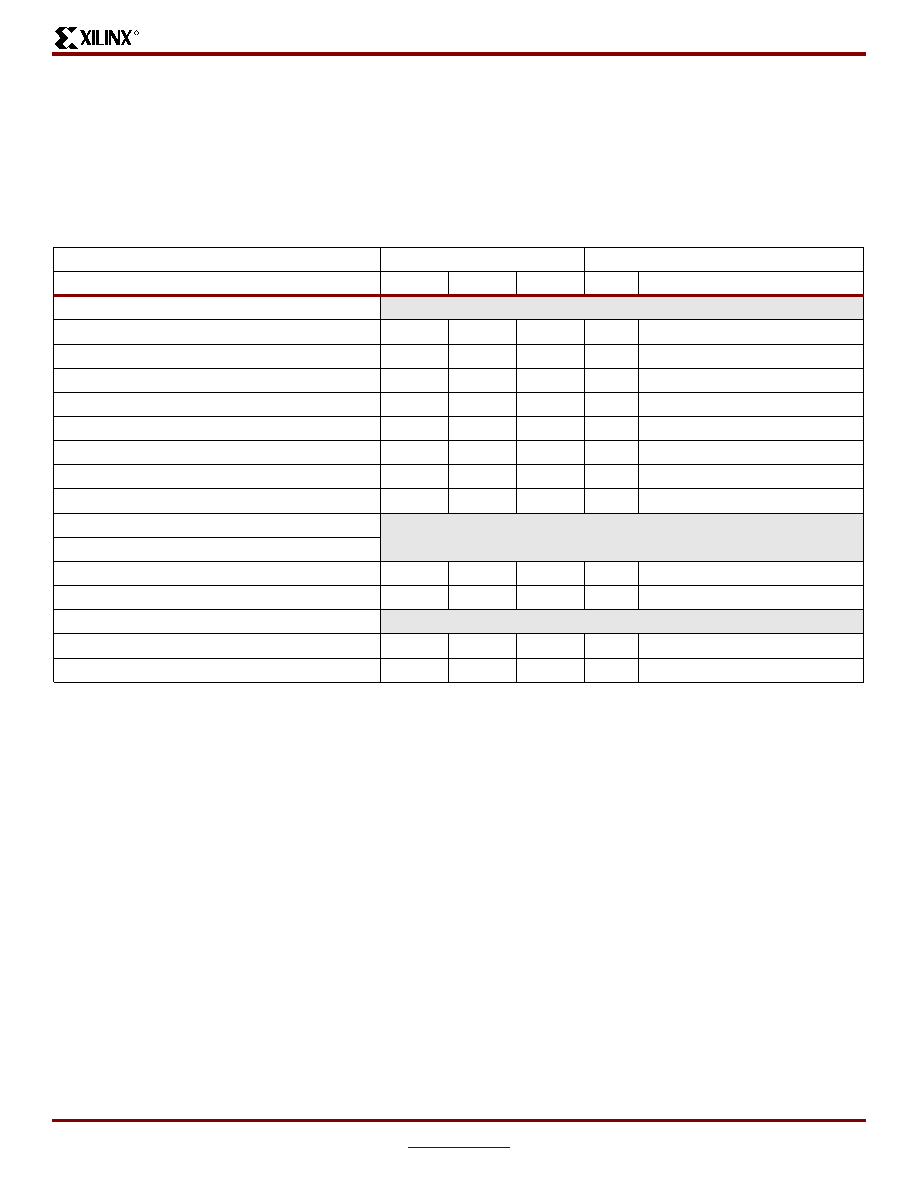
Virtex-II ProTM Platform FPGAs: DC and Switching Characteristics
R
DS083-3 (v2.12) November 11, 2003
www.xilinx.com
9
Advance Product Specification
1-800-255-7778
Virtex-II Pro
Performance Characteristics
This section provides the performance characteristics of
some common functions and designs implemented in
Virtex-II Pro devices. The numbers reported here are fully
characterized worst-case values. Note that these values are
subject to the same guidelines as
Virtex-II Pro Switching
Characteristics
(speed files).
Table 12
provides pin-to-pin values (in nanoseconds)
including IOB delays; that is, delay through the device from
input pin to output pin. In the case of multiple inputs and out-
puts, the worst delay is reported.
Table 12: Pin-to-Pin Performance
Pin-to-Pin (w/ I/O delays)
Description
-7
-6
-5
Units
Device Used & Speed Grade
Basic Functions:
16-bit Address Decoder
ns
XC2VP20FF1152-6
32-bit Address Decoder
ns
XC2VP20FF1152-6
64-bit Address Decoder
ns
XC2VP20FF1152-6
4:1 MUX
ns
XC2VP20FF1152-6
8:1 MUX
ns
XC2VP20FF1152-6
16:1 MUX
ns
XC2VP20FF1152-6
32:1 MUX
ns
XC2VP20FF1152-6
Combinatorial (pad to LUT to pad)
ns
XC2VP20FF1152-6
Memory:
Block RAM
Pad to setup
ns
XC2VP20FF1152-6
Clock to Pad
ns
XC2VP20FF1152-6
Distributed RAM
Pad to setup
ns
XC2VP20FF1152-6
Clock to Pad
ns
XC2VP20FF1152-6
Virtex-II Pro Performance Characteristics
R
10
www.xilinx.com
DS083-3 (v2.12) November 11, 2003
1-800-255-7778
Advance Product Specification
Table 13
shows internal (register-to-register) performance. Values are reported in MHz.
Table 13: Register-to-Register Performance
Register-to-Register
Performance
Description
-7
-6
-5
Units
Device Used & Speed Grade
Basic Functions:
16-bit Address Decoder
MHz
XC2VP20FF1152-6
32-bit Address Decoder
MHz
XC2VP20FF1152-6
64-bit Address Decoder
MHz
XC2VP20FF1152-6
4:1 MUX
MHz
XC2VP20FF1152-6
8:1 MUX
MHz
XC2VP20FF1152-6
16:1 MUX
MHz
XC2VP20FF1152-6
32:1 MUX
MHz
XC2VP20FF1152-6
Register to LUT to Register
MHz
XC2VP20FF1152-6
8-bit Adder
MHz
XC2VP20FF1152-6
16-bit Adder
MHz
XC2VP20FF1152-6
32-bit Adder
MHz
XC2VP20FF1152-6
64-bit Adder
MHz
XC2VP20FF1152-6
128-bit Adder
MHz
XC2VP20FF1152-6
24-bit Counter
MHz
XC2VP20FF1152-6
64-bit Counter
MHz
XC2VP20FF1152-6
64-bit Accumulator
MHz
XC2VP20FF1152-6
Multiplier 18x18 (with Block RAM inputs)
MHz
XC2VP20FF1152-6
Multiplier 18x18 (with Register inputs)
MHz
XC2VP20FF1152-6
Memory:
Block RAM
Single-Port 4096 x 4 bits
MHz
XC2VP20FF1152-6
Single-Port 2048 x 9 bits
MHz
XC2VP20FF1152-6
Single-Port 1024 x 18 bits
MHz
XC2VP20FF1152-6
Single-Port 512 x 36 bits
MHz
XC2VP20FF1152-6
Dual-Port A:4096 x 4 bits & B:1024 x 18 bits
MHz
XC2VP20FF1152-6
Dual-Port A:1024 x 18 bits & B:1024 x 18 bits
MHz
XC2VP20FF1152-6
Dual-Port A:2048 x 9 bits & B: 512 x 36 bits
MHz
XC2VP20FF1152-6
Distributed RAM
Single-Port 16 x 8-bit
MHz
XC2VP20FF1152-6
Single-Port 32 x 8-bit
MHz
XC2VP20FF1152-6
Single-Port 64 x 8-bit
MHz
XC2VP20FF1152-6
Single-Port 128 x 8-bit
MHz
XC2VP20FF1152-6
Dual-Port 16 x 8-bit
MHz
XC2VP20FF1152-6
Dual-Port 32 x 8-bit
MHz
XC2VP20FF1152-6
Dual-Port 64 x 8-bit
MHz
XC2VP20FF1152-6
Dual-Port 128 x 8-bit
MHz
XC2VP20FF1152-6
Virtex-II ProTM Platform FPGAs: DC and Switching Characteristics
R
DS083-3 (v2.12) November 11, 2003
www.xilinx.com
11
Advance Product Specification
1-800-255-7778
Shift Registers
128-bit SRL
MHz
XC2VP20FF1152-6
256-bit SRL
MHz
XC2VP20FF1152-6
FIFOs (Async. in Block RAM)
1024 x 18-bit
MHz
XC2VP20FF1152-6
1024 x 18-bit
MHz
XC2VP20FF1152-6
FIFOs (Sync. in SRL)
128 x 8-bit
MHz
XC2VP20FF1152-6
128 x 16-bit
MHz
XC2VP20FF1152-6
CAMs in Block RAM
32 x 9-bit
MHz
XC2VP20FF1152-6
64 x 9-bit
MHz
XC2VP20FF1152-6
128 x 9-bit
MHz
XC2VP20FF1152-6
256 x 9-bit
MHz
XC2VP20FF1152-6
CAMs in SRL
32 x 16-bit
MHz
XC2VP20FF1152-6
64 x 32-bit
MHz
XC2VP20FF1152-6
128 x 40-bit
MHz
XC2VP20FF1152-6
256 x 48-bit
MHz
XC2VP20FF1152-6
1024 x 16-bit
MHz
XC2VP20FF1152-6
1024 x 72-bit
MHz
XC2VP20FF1152-6
Table 13: Register-to-Register Performance (Continued)
Register-to-Register
Performance
Description
-7
-6
-5
Units
Device Used & Speed Grade
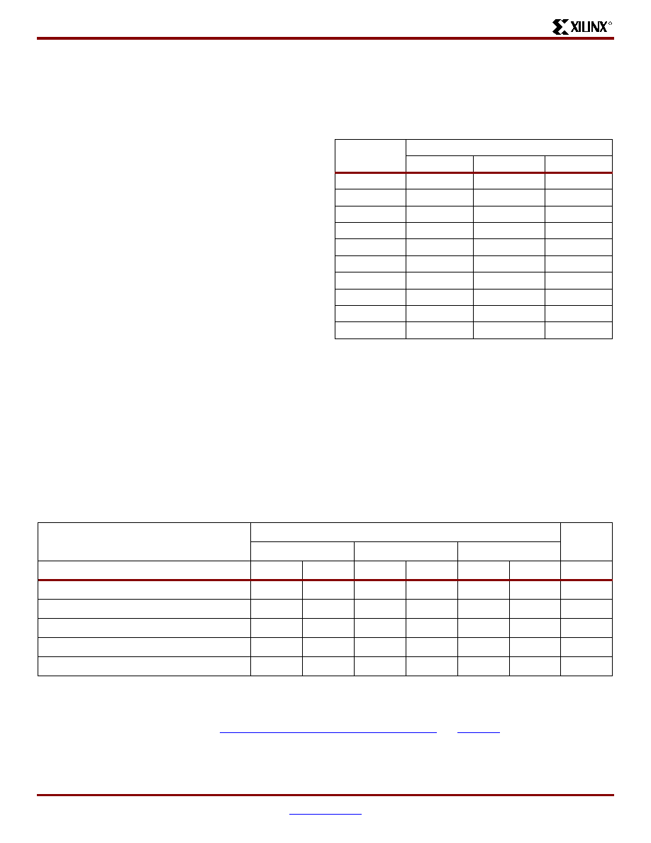
Virtex-II Pro Switching Characteristics
R
12
www.xilinx.com
DS083-3 (v2.12) November 11, 2003
1-800-255-7778
Advance Product Specification
Virtex-II Pro Switching Characteristics
Switching characteristics are specified on a
per-speed-grade basis and can be designated as Advance,
Preliminary, or Production. Note that
Virtex-II Pro Perfor-
mance Characteristics
are subject to these guidelines, as
well. Each designation is defined as follows:
Advance: These speed files are based on simulations only
and are typically available soon after device design specifi-
cations are frozen. Although speed grades with this desig-
nation are considered relatively stable and conservative,
some under-reporting might still occur.
Preliminary: These speed files are based on complete ES
(engineering sample) silicon characterization. Devices and
speed grades with this designation are intended to give a
better indication of the expected performance of production
silicon. The probability of under-reporting delays is greatly
reduced as compared to Advance data.
Production: These speed files are released once enough
production silicon of a particular device family member has
been characterized to provide full correlation between
speed files and devices over numerous production lots.
There is no under-reporting of delays, and customers
receive formal notification of any subsequent changes. Typ-
ically, the slowest speed grades transition to Production
before faster speed grades.
Since individual family members are produced at different
times, the migration from one category to another depends
completely on the status of the fabrication process for each
device.
Table 14
correlates the current status of each
Virtex-II Pro device with a corresponding speed file desig-
nation.
All specifications are always representative of worst-case
supply voltage and junction temperature conditions.
Testing of Switching Characteristics
All devices are 100% functionally tested. Internal timing
parameters are derived from measuring internal test pat-
terns. Listed below are representative values. For more
specific, more precise, and worst-case guaranteed data,
use the values reported by the static timing analyzer (TRCE
in the Xilinx Development System) and back-annotate to the
simulation net list. Unless otherwise noted, values apply to
all Virtex-II Pro devices.
PowerPC Switching Characteristics
Table 14: Virtex-II Pro Device Speed Grade
Designations
Device
Speed Grade Designations
Advance
Preliminary
Production
XC2VP2
-7, -6, -5
XC2VP4
-7, -6, -5
XC2VP7
-7
-6, -5
XC2VP20
-7
-6, -5
XC2VP30
-7
-6, -5
XC2VP40
-7
-6, -5
XC2VP50
-7
-6, -5
XC2VP70
-7
-6, -5
XC2VP100
XC2VP125
Table 15: Processor Clocks Absolute AC Characteristics
Speed Grade
-7
-6
-5
Description
Min
Max
Min
Max
Min
Max
Units
CPMC405CLOCK frequency
0
400
0
350
0
300
MHz
JTAGC405TCK frequency
(1)
0
200
0
175
0
150
MHz
PLBCLK
(2)
0
400
0
350
0
300
MHz
BRAMDSOCMCLK
(2)
0
400
0
350
0
300
MHz
BRAMISOCMCLK
(2)
0
400
0
350
0
300
MHz
Notes:
1.
The theoretical maximum frequency of this clock is one-half the CPMC405CLOCK. However, the achievable maximum is dependent
on the system, and will be much less.
2.
The theoretical maximum frequency of these clocks is equal to the CPMC405CLOCK. However, the achievable maximum is
dependent on the system. Please see
PowerPC 405 Processor Block Reference Guide
and
XAPP640
for more information.
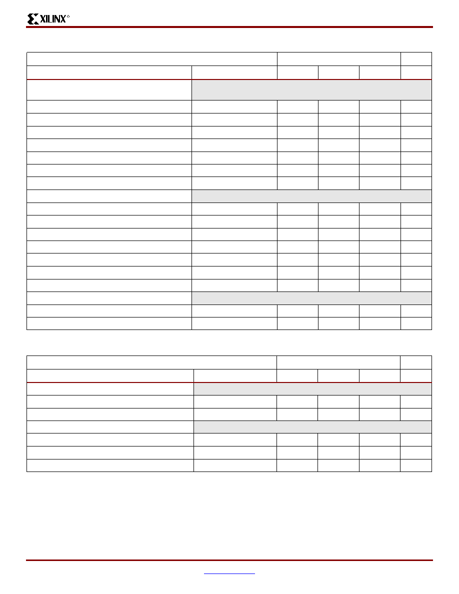
Virtex-II ProTM Platform FPGAs: DC and Switching Characteristics
R
DS083-3 (v2.12) November 11, 2003
www.xilinx.com
13
Advance Product Specification
1-800-255-7778
Table 16: Processor Block Switching Characteristics
Speed Grade
Description
Symbol
-7
-6
-5
Units
Setup and Hold Relative to Clock
(CPMC405CLOCK)
Device Control Register Bus control inputs
T
PCCK
_DCR/T
PCKC
_DCR
0.38/≠0.18
0.44/≠0.20
0.48/≠0.23
ns, min
Device Control Register Bus data inputs
T
PDCK
_DCR/T
PCKD
_DCR
0.65/≠0.01
0.75/≠0.01
0.82/≠0.02
ns, min
Clock and Power Management control inputs
T
PCCK
_CPM/T
PCKC
_CPM
0.16/ 0.03
0.19/ 0.03
0.20/ 0.03
ns, min
Reset control inputs
T
PCCK
_RST/T
PCKC
_RST
0.16/ 0.03
0.19/ 0.03
0.20/ 0.03
ns, min
Debug control inputs
T
PCCK
_DBG/T
PCKC
_DBG
0.27/ 0.30
0.31/ 0.35
0.34/ 0.38
ns, min
Trace control inputs
T
PCCK
_TRC/T
PCKC
_TRC
1.37/≠0.41
1.57/≠0.48
1.73/≠0.52
ns, min
External Interrupt Controller control inputs
T
PCCK
_EIC/T
PCKC
_EIC
0.57/≠0.22
0.66/≠0.25
0.72/≠0.27
ns, min
Clock to Out
Device Control Register Bus control outputs
T
PCKCO
_DCR
1.32
1.52
1.67
ns, max
Device Control Register Bus address outputs
T
PCKAO
_DCR
1.72
1.98
2.17
ns, max
Device Control Register Bus data outputs
T
PCKDO
_DCR
1.76
2.02
2.22
ns, max
Clock and Power Management control outputs
T
PCKCO
_CPM
1.26
1.45
1.59
ns, max
Reset control outputs
T
PCKCO
_RST
1.32
1.51
1.66
ns, max
Debug control outputs
T
PCKCO
_DBG
1.94
2.22
2.44
ns, max
Trace control outputs
T
PCKCO
_TRC
1.35
1.56
1.71
ns, max
Clock
CPMC405CLOCK minimum pulse width, high
T
CPWH
ns, min
CPMC405CLOCK minimum pulse width, low
T
CPWL
ns, min
Table 17: Processor Block PLB Switching Characteristics
Speed Grade
Description
Symbol
-7
-6
-5
Units
Setup and Hold Relative to Clock (PLBCLK)
Processor Local Bus(ICU/DCU) control inputs
T
PCCK
_PLB/T
PCKC
_PLB
0.98/ 0.18
1.12/ 0.21
1.23/ 0.23
ns, min
Processor Local Bus (ICU/DCU) data inputs
T
PDCK
_PLB/T
PCKD
_PLB
0.62/ 0.16
0.71/ 0.18
0.78/ 0.20
ns, min
Clock to Out
Processor Local Bus(ICU/DCU) control outputs
T
PCKCO
_PLB
1.34
1.54
1.69
ns, max
Processor Local Bus(ICU/DCU) address bus outputs
T
PCKAO
_PLB
1.16
1.34
1.47
ns, max
Processor Local Bus(ICU/DCU) data bus outputs
T
PCKDO
_PLB
1.44
1.65
1.81
ns, max

Virtex-II Pro Switching Characteristics
R
14
www.xilinx.com
DS083-3 (v2.12) November 11, 2003
1-800-255-7778
Advance Product Specification
Table 18: Processor Block JTAG Switching Characteristics
Speed Grade
Description
Symbol
-7
-6
-5
Units
Setup and Hold Relative to Clock (JTAGC405TCK)
JTAG control inputs
T
PCCK
_JTAG/
T
PCKC
_JTAG
0.80/ 0.70
0.80/ 0.70
0.88/ 0.77
ns, min
JTAG reset input
T
PCCK
_JTAGRST/
T
PCKC
_JTAGRST
0.80/ 0.70
0.80/ 0.70
0.88/ 0.77
ns, min
Clock to Out
JTAG control outputs
T
PCKCO
_JTAG
1.34
1.54
1.69
ns, max
Table 19: PowerPC 405 Data-Side On-Chip Memory Switching Characteristics
Speed Grade
Description
Symbol
-7
-6
-5
Units
Setup and Hold Relative to Clock
(BRAMDSOCMCLK)
Data-Side On-Chip Memory data bus inputs
T
PDCK
_DSOCM/
T
PCKD
_DSOCM
0.73/ 0.83
0.84/ 0.95
0.92/ 1.05
ns, min
Clock to Out
Data-Side On-Chip Memory control outputs
T
PCKCO
_DSOCM
1.58
1.82
1.99
ns, max
Data-Side On-Chip Memory address bus outputs
T
PCKAO
_DSOCM
1.46
1.68
1.84
ns, max
Data-Side On-Chip Memory data bus outputs
T
PCKDO
_DSOCM
0.90
1.03
1.13
ns, max
Table 20: PowerPC 405 Instruction-Side On-Chip Memory Switching Characteristics
Speed Grade
Description
Symbol
-7
-6
-5
Units
Setup and Hold Relative to Clock (BRAMISOCMCLK)
Instruction-Side On-Chip Memory data bus inputs
T
PDCK
_ISOCM/
T
PCKD
_ISOCM
0.81/ 0.68
0.93/ 0.78
1.02/ 0.86
ns, min
Clock to Out
Instruction-Side On-Chip Memory control outputs
T
PCKCO
_ISOCM
1.33
1.53
1.68
ns, max
Instruction-Side On-Chip Memory address bus outputs
T
PCKAO
_ISOCM
1.52
1.75
1.92
ns, max
Instruction-Side On-Chip Memory data bus outputs
T
PCKDO
_ISOCM
1.35
1.55
1.70
ns, max
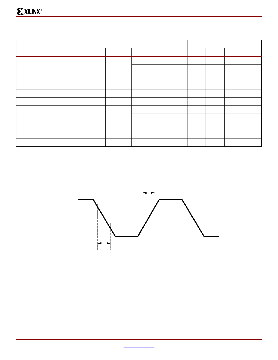
Virtex-II ProTM Platform FPGAs: DC and Switching Characteristics
R
DS083-3 (v2.12) November 11, 2003
www.xilinx.com
15
Advance Product Specification
1-800-255-7778
RocketIO Switching Characteristics
Table 21: RocketIO Reference Clock Switching Characteristics
All Speed Grades
Description
Symbol
Conditions
Min
Typ
Max
Units
Reference Clock frequency range
(1)
F
GCLK
Full rate operation
50
156.25
MHz
Half rate operation
60
100
MHz
Reference Clock frequency tolerance
F
GTOL
±100
ppm
Reference Clock rise time
T
RCLK
20% ≠ 80%
600
1000
ps
Reference Clock fall time
T
FCLK
20% ≠ 80%
600
1000
ps
Reference Clock duty cycle
T
DCREF
45
50
55
%
Reference Clock total jitter, peak-peak
(2)
T
GJTT
3.125 Gbps operation
40
ps
2.5 Gbps operation
50
ps
1.06 Gbps operation
120
ps
Clock recovery frequency acquisition time
T
LOCK
10
µs
Clock recovery phase acquisition time
T
PHASE
960
bits
Notes:
1.
BREFCLK/BREFCLK2 can be used for all serial bit rates up to the maximum shown. REFCLK/REFCLK2 can be used for serial bit
rates up to 2.5 Gb/s (REFCLK = 125 MHz). All other parameters apply equally to REFCLK, REFCLK2, BREFCLK, and BREFCLK2
except as noted.
2.
Measured at the package pin. For reference clock frequencies equal to or above 125 MHz, BREFCLK/BREFCLK2 must be used.
Figure 3: Reference Clock Timing Parameters
DS083-3_01_120302
80%
20%
T
FCLK
T
RCLK

Virtex-II Pro Switching Characteristics
R
16
www.xilinx.com
DS083-3 (v2.12) November 11, 2003
1-800-255-7778
Advance Product Specification
Table 22: RocketIO Receiver Switching Characteristics
Description
Symbol
Conditions
Min
Typ
Max
Units
Receive total jitter tolerance
T
JTOL
0.65
UI
(1)
Receive deterministic jitter tolerance
T
DJTOL
0.41
UI
Receive latency
(2)
T
RXLAT
25
42
RXUSRCLK cycles
RXUSRCLK duty cycle
T
RXDC
45
50
55
%
RXUSRCLK2 duty cycle
T
RX2DC
45
50
55
%
Bit error rate
BER
10
≠12
Notes:
1.
UI = Unit Interval
2.
Receive latency delay RXP/RXN to RXDATA. Refer to
RocketIO Transceiver User Guide
for more information on calculating latency.
Figure 4: Receive Latency (Maximum)
DS083-3_02_082301
RXDATA[16:0]
RXP/RXN
RXUSRCLK2
T
RXLAT
DATA ARRIVES
DATA ORIGINATES
0
1
41
42
1
2
. . . . .
20
821 822
. . . . .
. . . .
840 841 842
21
22
. . . . .
820

Virtex-II ProTM Platform FPGAs: DC and Switching Characteristics
R
DS083-3 (v2.12) November 11, 2003
www.xilinx.com
17
Advance Product Specification
1-800-255-7778
Table 23: RocketIO Transmitter Switching Characteristics
Description
Symbol
Conditions
Min
Typ
Max
Units
Serial data rate, full-speed clock
F
GTX
Flipchip packages
1.0
3.125
(1)
Gb/s
Wirebond packages
1.0
2.5
(1)
Gb/s
Serial data rate, half-speed clock
Flipchip packages
0.600
1.0
Gb/s
Wirebond packages
0.600
1.0
Gb/s
Serial data output deterministic jitter
T
DJ
0.17
UI
(2)
Serial data output random jitter
T
RJ
0.18
UI
TX rise time
T
RTX
20% ≠ 80%
120
ps
TX fall time
T
FTX
120
ps
Transmit latency
(3)
T
TXLAT
Including CRC
14
17
TXUSR
CLK
cycles
Excluding CRC
8
11
TXUSRCLK duty cycle
T
TXDC
45
50
55
%
TXUSRCLK2 duty cycle
T
TX2DC
45
50
55
%
Notes:
1.
Serial data rate in the -5 speed grade is limited to 2.0 Gb/s in both wirebond and flipchip packages.
2.
UI = Unit Interval
3.
Transmit latency delay TXDATA to TXP/TXN. Refer to
RocketIO Transceiver User Guide
for more information on calculating latency.
Figure 5: Transmit Latency (Maximum, Including CRC)
DS083-3_03_082301
TXP/TXN
TXDATA[16:0]
TXUSRCLK2
T
TXLAT
DATA ORIGINATES
1
0
2
1
. . . . .
16
17
20
321 322
. . . . .
. . . .
340 341 342
21
22
. . . . .
320
DATA ARRIVES
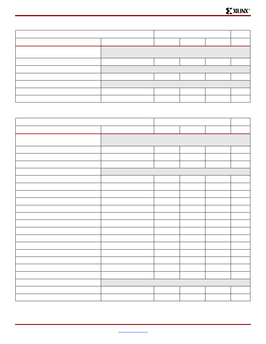
Virtex-II Pro Switching Characteristics
R
18
www.xilinx.com
DS083-3 (v2.12) November 11, 2003
1-800-255-7778
Advance Product Specification
Table 24: RocketIO RXUSRCLK Switching Characteristics
Speed Grade
Description
Symbol
-7
-6
-5
Units
Setup and Hold Relative to Clock
(RXUSRCLK)
CHBONDI control inputs
T
GCCK
_CHBI/T
GCKC
_CHBI
0.00/ 0.12
0.00/ 0.12
0.00/ 0.14
ns, min
Clock to Out
CHBONDO control outputs
T
GCKCO
_CHBO
0.50
0.50
0.55
ns, max
Clock
RXUSRCLK minimum pulse width, High
T
GPWH
_RX
0.80
0.80
0.88
ns, min
RXUSRCLK minimum pulse width, Low
T
GPWL
_RX
0.40
0.40
0.44
ns, min
Table 25: RocketIO RXUSRCLK2 Switching Characteristics
Speed Grade
Description
Symbol
-7
-6
-5
Units
Setup and Hold Relative to Clock
(RXUSRCLK2)
RXRESET control input
T
GCCK
_RRST/T
GCKC
_RRST
0.02/ 0.00
0.02/ 0.00
0.02/ 0.00
ns, min
RXPOLARITY control input
T
GCCK
_RPOL/T
GCKC
_RPOL
0.02/ 0.00
0.02/ 0.00
0.02/ 0.00
ns, min
ENCHANSYNC control input
T
GCCK
_ECSY/T
GCKC
_ECSY
0.02/ 0.00
0.02/ 0.00
0.02/ 0.00
ns, min
Clock to Out
RXNOTINTABLE status outputs
T
GCKST
_RNIT
0.50
0.50
0.55
ns, max
RXDISPERR status outputs
T
GCKST
_RDERR
0.50
0.50
0.55
ns, max
RXCHARISCOMMA status outputs
T
GCKST
_RCMCH
0.50
0.50
0.55
ns, max
RXREALIGN status output
T
GCKST
_ALIGN
0.41
0.41
0.46
ns, max
RXCOMMADET status output
T
GCKST
_CMDT
0.41
0.41
0.46
ns, max
RXLOSSOFSYNC status outputs
T
GCKST
_RLOS
0.50
0.50
0.55
ns, max
RXCLKCORCNT status outputs
T
GCKST
_RCCCNT
0.41
0.41
0.46
ns, max
RXBUFSTATUS status outputs
T
GCKST
_RBSTA
0.45
0.45
0.50
ns, max
RXCHECKINGCRC status output
T
GCKST
_RCCRC
0.36
0.40
0.44
ns, max
RXCRCERR status output
T
GCKST
_RCRCE
0.36
0.40
0.44
ns, max
CHBONDDONE status output
T
GCKST
_CHBD
0.50
0.50
0.55
ns, max
RXCHARISK status outputs
T
GCKST
_RKCH
0.50
0.50
0.55
ns, max
RXRUNDISP status outputs
T
GCKST
_RRDIS
0.50
0.50
0.55
ns, max
RXDATA data outputs
T
GCKDO
_RDAT
0.50
0.50
0.55
ns, max
Clock
RXUSRCLK2 minimum pulse width, High
T
GPWH
_RX2
1.44
1.44
2.25
ns, min
RXUSRCLK2 minimum pulse width, Low
T
GPWL
_RX2
0.72
0.72
1.13
ns, min

Virtex-II ProTM Platform FPGAs: DC and Switching Characteristics
R
DS083-3 (v2.12) November 11, 2003
www.xilinx.com
19
Advance Product Specification
1-800-255-7778
Table 26: RocketIO TXUSRCLK Switching Characteristics
Speed Grade
Description
Symbol
-7
-6
-5
Units
Setup and Hold Relative to Clock
(TXUSRCLK2)
CONFIGENABLE control input
T
GCCK
_CFGEN/T
GCKC
_CFGEN
0.35/ 0.10
0.35/ 0.10
0.39/ 0.11
ns, min
TXBYPASS8B10B control inputs
T
GCCK
_TBYP/T
GCKC
_TBYP
0.02/ 0.00
0.02/ 0.00
0.02/ 0.00
ns, min
TXFORCECRCERR control input
T
GCCK
_TCRCE/T
GCKC
_TCRCE
0.39/ 0.12
0.44/ 0.14
0.49/ 0.15
ns, min
TXPOLARITY control input
T
GCCK
_TPOL/T
GCKC
_TPOL
0.02/ 0.00
0.02/ 0.00
0.02/ 0.00
ns, min
TXINHIBIT control inputs
T
GCCK
_TINH/T
GCKC
_TINH
0.02/ 0.00
0.02/ 0.00
0.02/ 0.00
ns, min
LOOPBACK control inputs
T
GCCK
_LBK/T
GCKC
_LBK
0.02/ 0.00
0.02/ 0.00
0.02/ 0.00
ns, min
TXRESET control input
T
GCCK
_TRST/T
GCKC
_TRST
0.02/ 0.10
0.02/ 0.10
0.02/ 0.11
ns, min
TXCHARISK control inputs
T
GCCK
_TKCH/T
GCKC
_TKCH
0.02/ 0.00
0.02/ 0.00
0.02/ 0.00
ns, min
TXCHARDISPMODE control inputs
T
GCCK
_TCDM/T
GCKC
_TCDM
0.02/ 0.00
0.02/ 0.00
0.02/ 0.00
ns, min
TXCHARDISPVAL control inputs
T
GCCK
_TCDV/T
GCKC
_TCDV
0.02/ 0.00
0.02/ 0.00
0.02/ 0.00
ns, min
CONFIGIN data input
T
GDCK
_CFGIN/T
GCKD
_CFGIN
0.35/ 0.10
0.35/ 0.10
0.39/ 0.11
ns, min
TXDATA data inputs
T
GDCK
_TDAT/T
GCKD
_TDAT
0.02/ 0.00
0.02/ 0.00
0.02/ 0.00
ns, min
Clock to Out
TXBUFERR status output
T
GCKST
_TBERR
0.54
0.54
0.60
ns, max
TXKERR status outputs
T
GCKST
_TKERR
0.41
0.41
0.46
ns, max
TXRUNDISP status outputs
T
GCKST
_TRDIS
0.41
0.41
0.46
ns, max
CONFIGOUT data output
T
GCKDO
_CFGOUT
0.25
0.25
0.28
ns, max
Clock
TXUSRCLK minimum pulse width, High
T
GPWH
_TX
2.88
2.88
4.50
ns, min
TXUSRCLK minimum pulse width, Low
T
GPWL
_TX
1.44
1.44
2.25
ns, min
TXUSRCLK2 minimum pulse width, High
T
GPWH
_TX2
1.44
1.44
2.25
ns, min
TXUSRCLK2 minimum pulse width, Low
T
GPWL
_TX2
0.72
0.72
1.13
ns, min
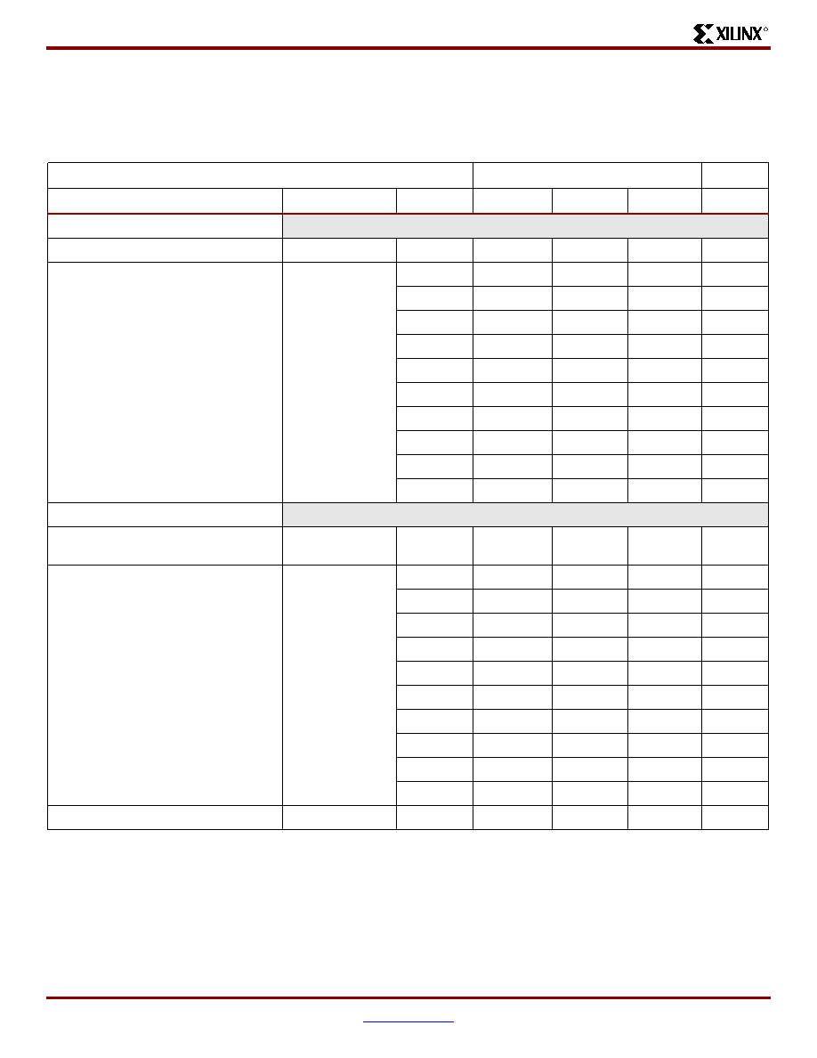
Virtex-II Pro Switching Characteristics
R
20
www.xilinx.com
DS083-3 (v2.12) November 11, 2003
1-800-255-7778
Advance Product Specification
IOB
Input Switching Characteristics
Input delays associated with the pad are specified for LVCMOS 2.5V levels. For other standards, adjust the delays with the
values shown in
IOB Input Switching Characteristics Standard Adjustments
.
Table 27: IOB Input Switching Characteristics
Speed Grade
Description
Symbol
Device
-7
-6
-5
Units
Propagation Delays
Pad to I output, no delay
T
IOPI
All
0.87
0.91
ns, max
Pad to I output, with delay
T
IOPID
XC2VP2
2.07
2.26
ns, max
XC2VP4
2.07
2.26
ns, max
XC2VP7
2.07
2.26
ns, max
XC2VP20
2.32
2.54
ns, max
XC2VP30
1.72
1.83
ns, max
XC2VP40
1.89
2.02
ns, max
XC2VP50
2.07
2.17
ns, max
XC2VP70
2.21
2.33
ns, max
XC2VP100
ns, max
XC2VP125
ns, max
Propagation Delays
Pad to output IQ via transparent latch,
no delay
T
IOPLI
All
0.89
0.93
ns, max
Pad to output IQ via transparent latch,
with delay
T
IOPLID
XC2VP2
4.76
5.21
ns, max
XC2VP4
4.76
5.21
ns, max
XC2VP7
4.76
5.21
ns, max
XC2VP20
3.62
3.86
ns, max
XC2VP30
3.77
4.01
ns, max
XC2VP40
4.31
4.57
ns, max
XC2VP50
4.92
5.11
ns, max
XC2VP70
4.99
5.19
ns, max
XC2VP100
ns, max
XC2VP125
ns, max
Clock CLK to output IQ
T
IOCKIQ
All
0.60
0.67
ns, max
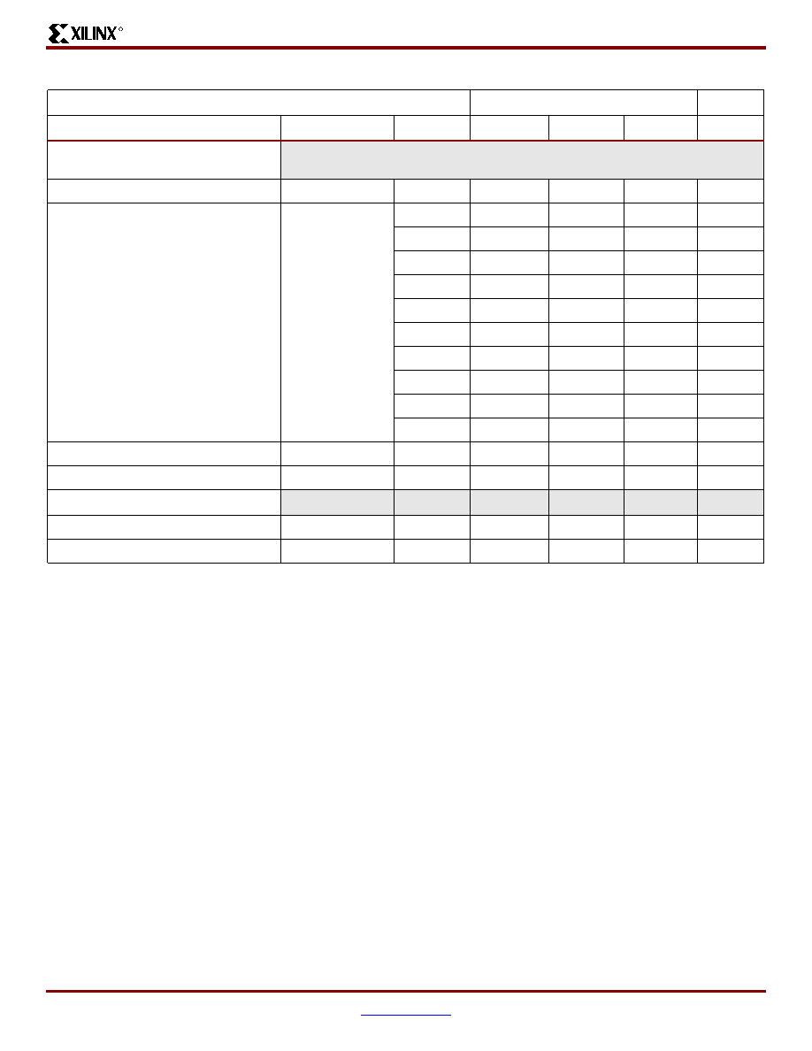
Virtex-II ProTM Platform FPGAs: DC and Switching Characteristics
R
DS083-3 (v2.12) November 11, 2003
www.xilinx.com
21
Advance Product Specification
1-800-255-7778
Setup and Hold Times With Respect to
Clock at IOB Input Register
Pad, no delay
T
IOPICK
/T
IOICKP
All
0.87/≠0.17
0.91/≠0.19
ns, min
Pad, with delay
T
IOPICKD
/T
IOICKPD
XC2VP2
4.74/≠3.27
5.19/≠3.62
ns, max
XC2VP4
4.74/≠3.27
5.19/≠3.62
ns, max
XC2VP7
4.74/≠3.27
5.19/≠3.62
ns, max
XC2VP20
3.60/≠2.36
3.84/≠2.53
ns, max
XC2VP30
3.75/≠2.48
3.99/≠2.65
ns, max
XC2VP40
4.29/≠2.91
4.55/≠3.10
ns, max
XC2VP50
4.90/≠3.40
5.09/≠3.54
ns, max
XC2VP70
4.97/≠3.46
5.17/≠3.59
ns, max
XC2VP100
ns, max
XC2VP125
ns, max
ICE input
T
IOICECK
/T
IOCKICE
All
0.44/ 0.01
0.49/ 0.01
ns, min
SR input (IFF, synchronous)
T
IOSRCKI
All
0.57
0.75
ns, min
Set/Reset Delays
SR input to IQ (asynchronous)
T
IOSRIQ
All
1.27
1.42
ns, max
GSR to output IQ
T
GSRQ
All
6.75
7.43
ns, max
Notes:
1.
Input timing for LVCMOS25 is measured at 1.25V. For other I/O standards, see
Table 31
.
Table 27: IOB Input Switching Characteristics (Continued)
Speed Grade
Description
Symbol
Device
-7
-6
-5
Units
Virtex-II Pro Switching Characteristics
R
22
www.xilinx.com
DS083-3 (v2.12) November 11, 2003
1-800-255-7778
Advance Product Specification
IOB Input Switching Characteristics Standard Adjustments
Table 28: IOB Input Switching Characteristics Standard Adjustments
Speed Grade
Description
Symbol
Standard
-7
-6
-5
Units
Data Input Delay Adjustments
Standard-specific data input delay
adjustments
T
ILVTTL
LVTTL
0.08
0.09
ns
T
ILVCMOS33
LVCMOS
0.05
0.05
ns
T
ILVCMOS25
LVCMOS25
0.00
0.00
ns
T
ILVCMOS18
LVCMOS18
0.33
0.36
ns
T
ILVCMOS15
LVCMOS15
0.41
0.45
ns
T
ILVDS_25
LVDS_25
0.36
0.40
ns
T
ILVDS_25_DT
LVDS_25_DT
0.36
0.40
ns
T
IPCI33_3
PCI, 33 MHz, 3.3V
0.16
0.18
ns
T
IPCI66_3
PCI, 66 MHz, 3.3V
0.17
0.19
ns
T
IPCIX
PCI-X
0.13
0.15
ns
T
IGTL
GTL
0.68
0.74
ns
T
IGTLP
GTLP
0.72
0.79
ns
T
IHSTL_I
HSTL_I
0.68
0.75
ns
T
IHSTL_II
HSTL_II
0.68
0.75
ns
T
IHSTL_III
HSTL_III
0.66
0.72
ns
T
IHSTL_IV
HSTL_IV
0.67
0.74
ns
T
IHSTL_I_18
HSTL_I_18
0.65
0.72
ns
T
IHSTL_II_18
HSTL_II_18
0.63
0.69
ns
T
IHSTL_III_18
HSTL_III_18
0.64
0.70
ns
T
IHSTL_IV_18
HSTL_IV_18
0.65
0.71
ns
T
ISSTL2_I
SSTL2_I
0.72
0.79
ns
T
ISSTL2_II
SSTL2_II
0.73
0.81
ns
T
ILVDCI33
LVDCI_33
≠0.05
≠0.06
ns
T
ILVDCI25
LVDCI_25
0.00
0.00
ns
T
ILVDCI18
LVDCI_18
0.09
0.09
ns
T
ILVDCI15
LVDCI_15
0.15
0.17
ns
T
ILVDCI_DV2_25
LVDCI_DV2_25
0.00
0.00
ns
T
ILVDCI_DV2_18
LVDCI_DV2_18
0.09
0.09
ns
T
ILVDCI_DV2_15
LVDCI_DV2_15
0.15
0.17
ns
T
IGTL_DCI
GTL_DCI
0.57
0.62
ns
T
IGTLP_DCI
GTLP_DCI
0.31
0.35
ns
T
IHSTL_I_DCI
HSTL_I_DCI
0.31
0.35
ns
T
IHSTL_II_DCI
HSTL_II_DCI
0.31
0.35
ns
T
IHSTL_III_DCI
HSTL_III_DCI
0.31
0.35
ns
Virtex-II ProTM Platform FPGAs: DC and Switching Characteristics
R
DS083-3 (v2.12) November 11, 2003
www.xilinx.com
23
Advance Product Specification
1-800-255-7778
Standard-specific data input delay
adjustments (continued)
T
IHSTL_IV_DCI
HSTL_IV_DCI
0.31
0.35
ns
T
IHSTL_I_DCI_18
HSTL_I_DCI_18
0.31
0.35
ns
T
IHSTL_II_DCI_18
HSTL_II_DCI_18
0.31
0.35
ns
T
IHSTL_III_DCI_18
HSTL_III_DCI_18
0.31
0.35
ns
T
IHSTL_IV_DCI_18
HSTL_IV_DCI_18
0.31
0.35
ns
T
ISSTL2_I_DCI
SSTL2_I_DCI
0.20
0.22
ns
T
ISSTL2_II_DCI
SSTL2_II_DCI
0.20
0.22
ns
T
ILVDSEXT_25
LVDSEXT_25
0.37
0.41 ns
T
ILVDSEXT_25_DT
LVDSEXT_25_DT
0.37
0.41 ns
T
ILDT_25
LDT_25
0.36
0.40
ns
T
ILDT_25_DT
LDT_25_DT
0.36
0.40
ns
T
IBLVDS_25
BLVDS_25
0.00
0.00
ns
T
IULVDS_25
ULVDS_25
0.36
0.40
ns
T
IULVDS_25_DT
ULVDS_25_DT
0.36
0.40
ns
T
ILVDS_25_DCI
LVDS_25_DCI
0.36
0.40
ns
T
ILVDSEXT_25_DCI
LVDSEXT_25_DCI
0.37
0.41
ns
T
ILVPECL_25
LVPECL_25
0.80
0.88
ns
T
ISSTL18_I
SSTL18_I
0.72
0.79
ns
T
ISSTL18_II
SSTL18_II
0.73
0.81
ns
T
ISSTL18_I_DCI
SSTL18_I_DCI
0.72
0.79
ns
T
ISSTL18_II_DCI
SSTL18_II_DCI
0.73
0.81
ns
Table 28: IOB Input Switching Characteristics Standard Adjustments (Continued)
Speed Grade
Description
Symbol
Standard
-7
-6
-5
Units
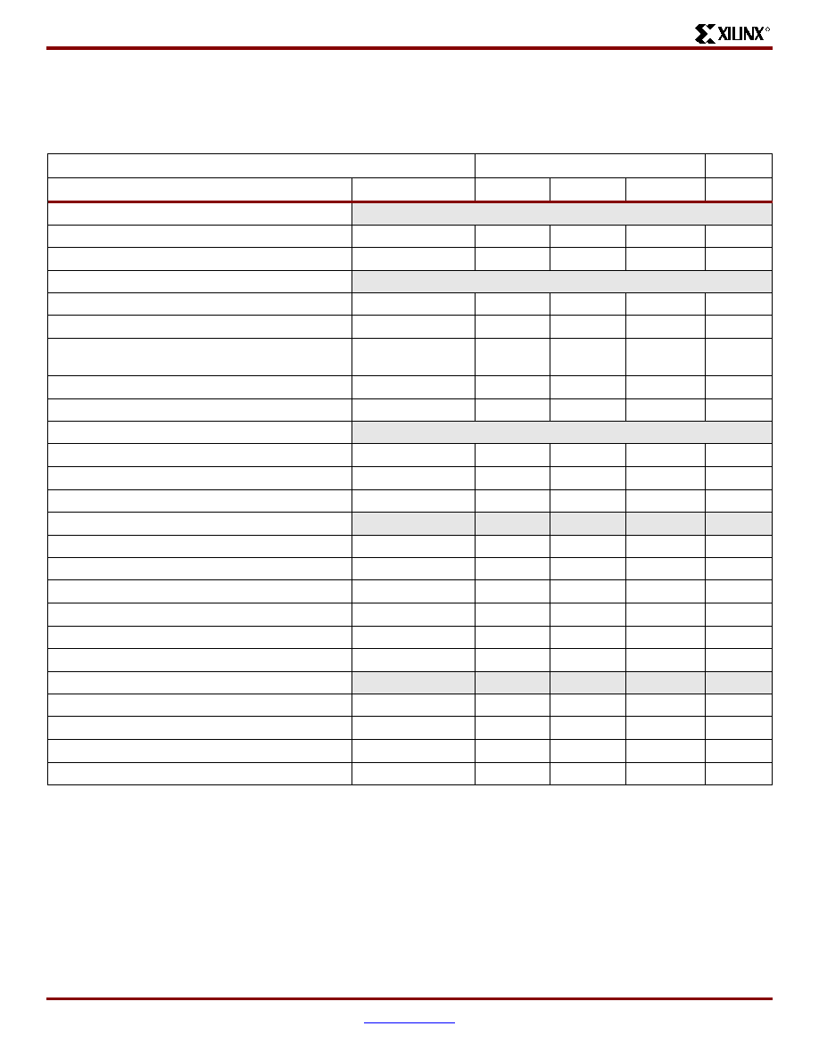
Virtex-II Pro Switching Characteristics
R
24
www.xilinx.com
DS083-3 (v2.12) November 11, 2003
1-800-255-7778
Advance Product Specification
IOB Output Switching Characteristics
Output delays terminating at a pad are specified for LVCMOS25 with 12 mA drive and fast slew rate. For other standards,
adjust the delays with the values shown in
IOB Output Switching Characteristics Standard Adjustments
.
Table 29: IOB Output Switching Characteristics
Speed Grade
Description
Symbol
-7
-6
-5
Units
Propagation Delays
O input to Pad
T
IOOP
2.33
2.55
ns, max
O input to Pad via transparent latch
T
IOOLP
2.47
2.69
ns, max
3-State Delays
T input to Pad high-impedance
(2)
T
IOTHZ
1.36
1.53
ns, max
T input to valid data on Pad
T
IOTP
2.28
2.48
ns, max
T input to Pad high-impedance via
transparent latch
(2)
T
IOTLPHZ
1.23
1.38
ns, max
T input to valid data on Pad via transparent latch
T
IOTLPON
2.34
2.55
ns, max
GTS to Pad high-impedance
(2)
T
GTS
4.73
5.20
ns, max
Sequential Delays
Clock CLK to Pad
T
IOCKP
2.41
2.63
ns, max
Clock CLK to Pad high-impedance (synchronous)
(2)
T
IOCKHZ
1.56
1.75
ns, max
Clock CLK to valid data on Pad (synchronous)
T
IOCKON
2.47
2.70
ns, max
Setup and Hold Times Before/After Clock CLK
O input
T
IOOCK
/T
IOCKO
0.26/ 0.14
0.29/ 0.15
ns, min
OCE input
T
IOOCECK
/T
IOCKOCE
0.44/ 0.01
0.49/ 0.01
ns, min
SR input (OFF)
T
IOSRCKO
/T
IOCKOSR
0.57/ 0.00
0.75/ 0.00
ns, min
3≠State Setup Times, T input
T
IOTCK
/T
IOCKT
0.26/ 0.14
0.29/ 0.15
ns, min
3-State Setup Times, TCE input
T
IOTCECK
/T
IOCKTCE
0.44/ 0.01
0.49/ 0.01
ns, min
3-State Setup Times, SR input (TFF)
T
IOSRCKT
/T
IOCKTSR
0.57/ 0.00
0.75/ 0.00
ns, min
Set/Reset Delays
SR input to Pad (asynchronous)
T
IOSRP
3.21
3.53
ns, max
SR input to Pad high-impedance (asynchronous)
(2)
T
IOSRHZ
2.17
2.44
ns, max
SR input to valid data on Pad (asynchronous)
T
IOSRON
3.09
3.39
ns, max
GSR to Pad
T
IOGSRQ
6.75
7.43
ns, max
Notes:
1.
A Zero "0" Hold Time listing indicates no hold time or a negative hold time. Negative values can not be guaranteed "best-case", but
if a "0" is listed, there is no positive hold time.
2.
The 3-state turn-off delays should not be adjusted.

Virtex-II ProTM Platform FPGAs: DC and Switching Characteristics
R
DS083-3 (v2.12) November 11, 2003
www.xilinx.com
25
Advance Product Specification
1-800-255-7778
IOB Output Switching Characteristics Standard Adjustments
Output delays terminating at a pad are specified for LVCMOS25 with 12 mA drive and fast slew rate. For other standards,
adjust the delays by the values shown.
Table 30: IOB Output Switching Characteristics Standard Adjustments
Output Delay Adjustments
Speed Grade
Description
Symbol
Standard
-7
-6
-5
Units
Standard-specific adjustments for
output delays terminating at pads
(based on standard capacitive load,
Csl)
T
OLVDS_25
LVDS 0.01
0.01
ns
T
OLVDSEXT_25
LVDSEXT 0.15
0.16
ns
T
OLDT_25
LDT 0.14
0.16
ns
T
OBLVDS_25
BLVDS
0.00
0.00
ns
T
OULVDS_25
ULVDS
0.14
0.16
ns
T
OPCI33_3
PCI, 33 MHz, 3.3V
0.75
0.83
ns
T
OPCI66_3
PCI, 66 MHz, 3.3V
0.79
0.87
ns
T
OPCIX
PCI-X
0.79
0.87
ns
T
OGTL
GTL
1.41
1.55
ns
T
OGTLP
GTLP
2.69
2.96
ns
T
OHSTL_I
HSTL_I
0.64
0.70
ns
T
OHSTL_II
HSTL_II
0.35
0.38
ns
T
OHSTL_IIII
HSTL_III
0.35
0.39
ns
T
OHSTL_IV
HSTL_IV
0.17
0.19
ns
T
OHSTL_I_18
HSTL_I_18
0.64
0.70
ns
T
OHSTL_II_18
HSTL_II_18
0.35
0.38
ns
T
OHSTL_IIII_18
HSTL_III_18
0.41
0.45
ns
T
OHSTL_IV_18
HSTL_IV_18
0.22
0.24
ns
T
OSSTL2_I
SSTL2_I
0.72
0.79
ns
T
OSSTL2_II
SSTL2_II
0.25
0.27
ns
T
OLVTTL_S2
LVTTL, Slow, 2 mA
6.24
6.86
ns
T
OLVTTL_S4
4 mA
3.55
3.91
ns
T
OLVTTL_S6
6 mA
2.60
2.86
ns
T
OLVTTL_S8
8 mA
1.69
1.86
ns
T
OLVTTL_S12
12 mA
1.18
1.29
ns
T
OLVTTL_S16
16 mA
0.53
0.58
ns
T
OLVTTL_S24
24 mA
0.42
0.47
ns
T
OLVTTL_F2
LVTTL, Fast, 2 mA
5.09
5.59
ns
T
OLVTTL_F4
4 mA
2.24
2.46
ns
T
OLVTTL_F6
6 mA
1.26
1.39
ns
T
OLVTTL_F8
8 mA
0.46
0.51
ns
T
OLVTTL_F12
12 mA
0.27
0.30
ns
T
OLVTTL_F16
16 mA
0.06
0.07
ns
T
OLVTTL_F24
24 mA
≠0.01
≠0.01
ns
T
OLVCMOS33_S2
LVCMOS33, Slow, 2 mA
6.23
6.86
ns
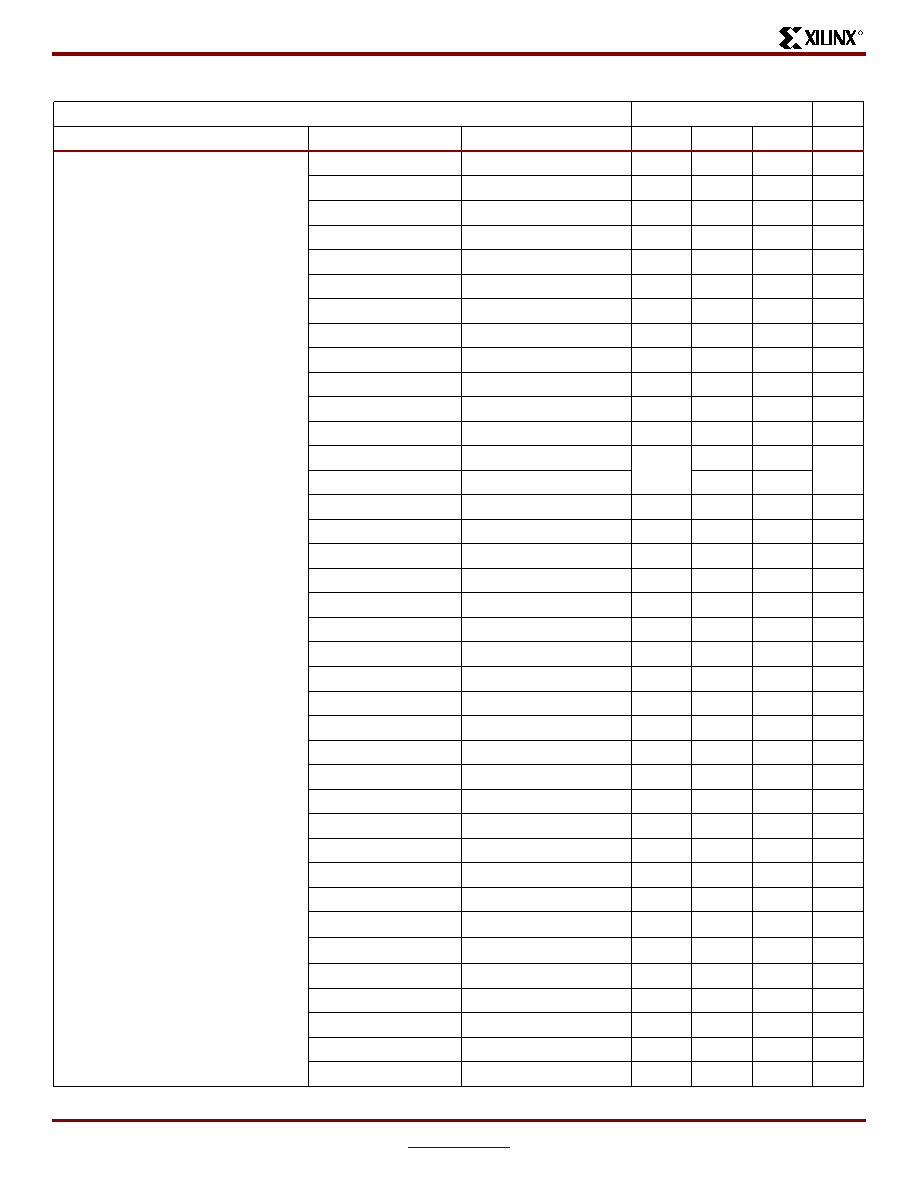
Virtex-II Pro Switching Characteristics
R
26
www.xilinx.com
DS083-3 (v2.12) November 11, 2003
1-800-255-7778
Advance Product Specification
Standard-specific adjustments for
output delays terminating at pads
(based on standard capacitive load,
Csl)
T
OLVCMOS33_S4
4 mA
3.61
3.97
ns
T
OLVCMOS33_S6
6 mA
2.60
2.86
ns
T
OLVCMOS33_S8
8 mA
1.69
1.86
ns
T
OLVCMOS33_S12
12 mA
1.18
1.30
ns
T
OLVCMOS33_S16
16 mA
0.52
0.57
ns
T
OLVCMOS33_S24
24 mA
0.44
0.49
ns
T
OLVCMOS33_F2
LVCMOS33, Fast, 2 mA
5.13
5.64
ns
T
OLVCMOS33_F4
4 mA
2.25
2.48
ns
T
OLVCMOS33_F6
6 mA
1.28
1.40
ns
T
OLVCMOS33_F8
8 mA
0.47
0.52
ns
T
OLVCMOS33_F12
12 mA
0.26
0.28
ns
T
OLVCMOS33_F16
16 mA
0.02
0.03
ns
T
OLVCMOS33_F24
24 mA
≠0.08
≠0.09
ns
T
OLVCMOS25_S2
LVCMOS25, Slow, 2 mA
4.74
5.21
ns
T
OLVCMOS25_S4
4 mA
2.80
3.07
ns
T
OLVCMOS25_S6
6 mA
2.02
2.22
ns
T
OLVCMOS25_S8
8 mA
1.19
1.31
ns
T
OLVCMOS25_S12
12 mA
0.87
0.96
ns
T
OLVCMOS25_S16
16 mA
0.47
0.52
ns
T
OLVCMOS25_S24
24 mA
0.26
0.28
ns
T
OLVCMOS25_F2
LVCMOS25, Fast, 2 mA
3.78
4.16
ns
T
OLVCMOS25_F4
4 mA
1.50
1.65
ns
T
OLVCMOS25_F6
6 mA
0.71
0.78
ns
T
OLVCMOS25_F8
8 mA
0.23
0.25
ns
T
OLVCMOS25_F12
12 mA
0.00
0.00
ns
T
OLVCMOS25_F16
16 mA
≠0.03
≠0.04
ns
T
OLVCMOS25_F24
24 mA
≠0.18
≠0.20
ns
T
OLVCMOS18_S2
LVCMOS18, Slow, 2 mA
4.83
5.31
ns
T
OLVCMOS18_S4
4 mA
3.18
3.49
ns
T
OLVCMOS18_S6
6 mA
2.20
2.41
ns
T
OLVCMOS18_S8
8 mA
2.20
2.42
ns
T
OLVCMOS18_S12
1 mA
1.81
1.99
ns
T
OLVCMOS18_S16
16 mA
0.87
0.96
ns
T
OLVCMOS18_F2
LVCMOS18, Fast, 2 mA
2.69
2.95
ns
T
OLVCMOS18_F4
4 mA
0.81
0.89
ns
T
OLVCMOS18_F6
6 mA
0.57
0.63
ns
T
OLVCMOS18_F8
8 mA
0.55
0.61
ns
T
OLVCMOS18_F12
12 mA
0.34
0.38
ns
Table 30: IOB Output Switching Characteristics Standard Adjustments (Continued)
Output Delay Adjustments
Speed Grade
Description
Symbol
Standard
-7
-6
-5
Units

Virtex-II ProTM Platform FPGAs: DC and Switching Characteristics
R
DS083-3 (v2.12) November 11, 2003
www.xilinx.com
27
Advance Product Specification
1-800-255-7778
Standard-specific adjustments for
output delays terminating at pads
(based on standard capacitive load,
Csl)
T
OLVCMOS18_F16
16 mA
0.12
0.13
ns
T
OLVCMOS15_S2
LVCMOS15, Slow, 2 mA
7.12
7.83
ns
T
OLVCMOS15_S4
4 mA
4.93
5.42
ns
T
OLVCMOS15_S6
6 mA
3.24
3.56
ns
T
OLVCMOS15_S8
8 mA
2.93
3.23
ns
T
OLVCMOS15_S12
12 mA
1.51
1.66
ns
T
OLVCMOS15_S16
16 mA
1.47
1.62
ns
T
OLVCMOS15_F2
LVCMOS15, Fast, 2 mA
2.60
2.86
ns
T
OLVCMOS15_F4
4 mA
1.90
2.09
ns
T
OLVCMOS15_F6
6 mA
0.75
0.82
ns
T
OLVCMOS15_F8
8 mA
1.08
1.19
ns
T
OLVCMOS15_F12
12 mA
0.29
0.32
ns
T
OLVCMOS15_F16
16 mA
0.32
0.35
ns
T
OLVDCI33
LVDCI_33
0.83
0.91
ns
T
OLVDCI25
LVDCI_25
0.64
0.71
ns
T
OLVDCI18
LVDCI_18
0.75
0.82
ns
T
OLVDCI15
LVDCI_15
1.15
1.26
ns
T
OLVDCI_DV2_25
LVDCI_DV2_25
0.07
0.08
ns
T
OLVDCI_DV2_18
LVDCI_DV2_18
0.34
0.38
ns
T
OLVDCI_DV2_15
LVDCI_DV2_15
0.69
0.76
ns
T
OGTL_DCI
GTL_DCI
1.39
1.53
ns
T
OGTLP_DCI
GTLP_DCI
2.71
2.98
ns
T
OHSTL_I_DCI
HSTL_I_DCI
0.63
0.69
ns
T
OHSTL_II_DCI
HSTL_II_DCI
0.54
0.60
ns
T
OHSTL_III_DCI
HSTL_III_DCI
0.36
0.40
ns
T
OHSTL_IV_DCI
HSTL_IV_DCI
2.08
2.29
ns
T
OHSTL_I_DCI_18
HSTL_I_DCI_18
0.63
0.70
ns
T
OHSTL_II_DCI_18
HSTL_II_DCI_18
0.28
0.31
ns
T
OHSTL_III_DCI_18
HSTL_III_DCI_18
0.40
0.44
ns
T
OHSTL_IV_DCI_18
HSTL_IV_DCI_18
1.70
1.87
ns
T
OSSTL2_I_DCI
SSTL2_I_DCI
0.56
0.61
ns
T
OSSTL2_II_DCI
SSTL2_II_DCI
0.56
0.61
ns
T
OLVPECL_25
LVPECL_25
0.19
0.21
ns
T
OSSTL18_I
SSTL18_I
0.92
1.01
ns
T
OSSTL18_II
SSTL18_II
0.51
0.56
ns
T
OSSTL18_I_DCI
SSTL18_I_DCI
0.62
0.68
ns
T
OSSTL18_II_DCI
SSTL18_II_DCI
0.28
0.31
ns
Table 30: IOB Output Switching Characteristics Standard Adjustments (Continued)
Output Delay Adjustments
Speed Grade
Description
Symbol
Standard
-7
-6
-5
Units
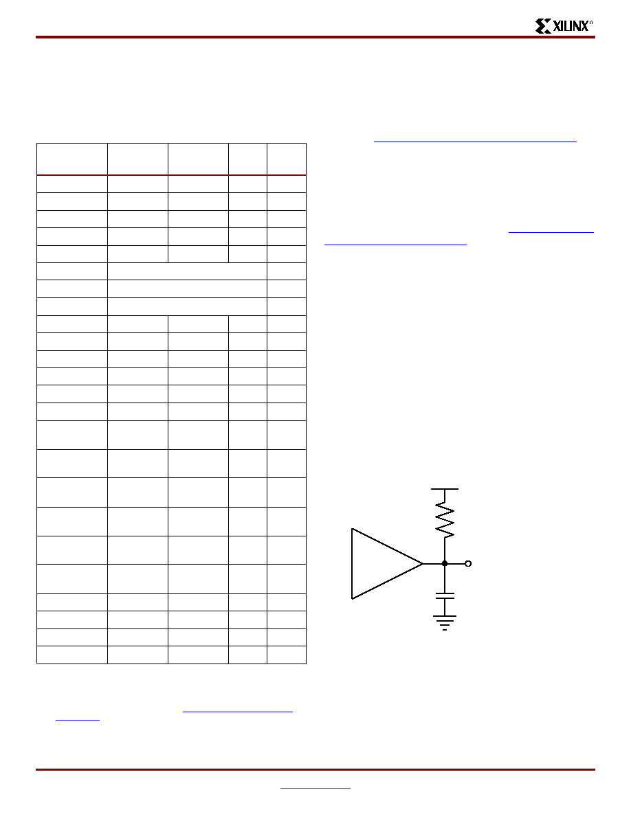
Virtex-II Pro Switching Characteristics
R
28
www.xilinx.com
DS083-3 (v2.12) November 11, 2003
1-800-255-7778
Advance Product Specification
I/O
Standard Adjustment Measurement Methodology
Input Delay Measurements
Table 31
shows the test setup parameters used for measur-
ing Input standard adjustments (see
Table 28, page 22
).
Output Delay Measurements
Output delays are measured using a Tektronix P6245
TDS500/600 probe (< 1 pf) across approximately 4" of FR4
microstrip trace. Standard termination was used for all test-
ing. (See
Virtex-II Pro Platform FPGA User Guide
for
details.) The propagation delay of the 4" trace is character-
ized separately and subtracted from the final measurement,
and is therefore not included in the generalized test setup
shown in
Figure 6
.
Measurements and test conditions are reflected in the IBIS
models except where the IBIS format precludes it. (IBIS
models can be found on the web at
http://support.xil-
inx.com/support/sw_ibis.htm
.) Parameters V
REF
, R
REF
,
C
REF
, and V
MEAS
fully describe the test conditions for each
I/O standard. The most accurate prediction of propagation
delay in any given application can be obtained through IBIS
simulation, using the following method:
1.
Simulate the output driver of choice into the generalized
test setup, using values from
Table 32
.
2.
Record the time to V
MEAS
.
3.
Simulate the output driver of choice into the actual PCB
trace and load, using the appropriate IBIS model or
capacitance value to represent the load.
4.
Record the time to V
MEAS
.
5.
Compare the results of steps 2 and 4. The increase or
decrease in delay should be added to or subtracted
from the I/O Output Standard Adjustment value
(
Table 30
) to yield the actual worst-case propagation
delay (clock-to-input) of the PCB trace.
Table 31: Input Delay Measurement Methodology
Standard
V
L
(1)
V
H
(1)
V
MEAS
(3,4)
V
REF
(2,4)
LVTTL
0
3.3
1.65
≠
LVCMOS33
0
3.3
1.65
≠
LVCMOS25
0
2.5
1.25
≠
LVCMOS18
0
1.8
0.9
≠
LVCMOS15
0
1.5
0.75
≠
PCI33_3
Per PCI Specification
≠
PCI66_3
Per PCI Specification
≠
PCI-X
Per PCI-X Specification
≠
GTL
V
REF
≠ 0.2
V
REF
+ 0.2
V
REF
0.80
GTLP
V
REF
≠ 0.2
V
REF
+ 0.2
V
REF
1.0
HSTL Class I
V
REF
≠ 0.5
V
REF
+ 0.5
V
REF
0.75
HSTL Class II
V
REF
≠ 0.5
V
REF
+ 0.5
V
REF
0.75
HSTL Class III
V
REF
≠ 0.5
V
REF
+ 0.5
V
REF
0.90
HSTL Class IV
V
REF
≠ 0.5
V
REF
+ 0.5
V
REF
0.90
HSTL18
Class I
V
REF
≠ 0.5
V
REF
+ 0.5
V
REF
0.90
HSTL18
Class II
V
REF
≠ 0.5
V
REF
+ 0.5
V
REF
0.90
HSTL18
Class III
V
REF
≠ 0.5
V
REF
+ 0.5
V
REF
1.08
HSTL18
Class IV
V
REF
≠ 0.5
V
REF
+ 0.5
V
REF
1.08
SSTL2
Class I & II
V
REF
≠ 0.75
V
REF
+ 0.75
V
REF
1.25
SSTL18
Class I & II
V
REF
≠ 0.5
V
REF
+ 0.5
V
REF
0.9
LVDS25
1.2 ≠ 0.125
1.2 + 0.125
1.2
LVDSEXT25
1.2 ≠ 0.125
1.2 + 0.125
1.2
ULVDS25
0.6 ≠ 0.125
0.6 + 0.125
0.6
LDT25
0.6 ≠ 0.125
0.6 + 0.125
0.6
Notes:
1.
Input waveform switches between V
L
and V
H
.
2.
Measurements are made at typical, minimum, and maximum V
REF
values. Reported delays reflect worst case of these measurements.
V
REF
values listed are typical. See
Virtex-II Pro Platform FPGA
User Guide
for min/max specifications.
3.
Input voltage level from which measurement starts.
4.
Note that this is an input voltage reference that bears no relation to
the V
REF
/ V
MEAS
parameters found in IBIS models and/or noted in
Figure 6
.
Figure 6: Generalized Test Setup
V
REF
R
REF
V
MEAS
(voltage level at which
delay measurement is taken)
C
REF
(probe capacitance)
FPGA Output
ds083-3_06a_092503
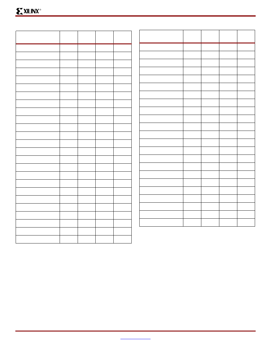
Virtex-II ProTM Platform FPGAs: DC and Switching Characteristics
R
DS083-3 (v2.12) November 11, 2003
www.xilinx.com
29
Advance Product Specification
1-800-255-7778
Table 32: Output Delay Measurement Methodology
Standard
R
REF
(ohms)
C
REF
(1)
(pF)
V
MEAS
(V)
V
REF
(V)
LVTTL (all)
1M
0
1.4
0
LVCMOS33
1M
0
1.65
0
LVCMOS25
1M
0
1.25
0
LVCMOS18
1M
0
0.9
0
LVCMOS15
1M
0
0.75
0
PCI33_3 - rising edge
25
0
0.94
0
PCI33_3 - falling edge
25
0
2.03
3.3
PCI66_3 - rising edge
25
0
0.94
0
PCI66_3 - falling edge
25
0
2.03
3.3
PCI-X - rising edge
25
0
0.94
PCI-X - falling edge
25
0
2.03
3.3
GTL
25
0
0.8
1.2
GTLP
25
0
1.0
1.5
HSTL Class I
50
0
V
REF
0.75
HSTL Class II
25
0
V
REF
0.75
HSTL Class III
50
0
0.9
1.5
HSTL Class IV
25
0
0.9
1.5
HSTL18 Class I
50
0
V
REF
0.9
HSTL18 Class II
25
0
V
REF
0.9
HSTL18 Class III
50
0
1.1
1.8
HSTL18 Class IV
25
0
1.1
1.8
SSTL2 Class I
50
0
V
REF
1.25
SSTL2 Class II
25
0
V
REF
1.25
SSTL18 Class I
50
0
V
REF
0.9
SSTL18 Class II
25
0
V
REF
0.9
LVDS25
50
0
V
REF
1.2
LVDSEXT25
50
0
V
REF
1.2
BLVDS
1M
0
1.2
0
LDT25
50
0
V
REF
0.6
LVPECL25
1M
0
1.23
0
LVDCI33
1M
0
1.65
0
LVDCI25
1M
0
1.25
0
LVDCI18
1M
0
0.9
0
LVDCI15
1M
0
0.75
0
HSTL DCI Class I
50
0
V
REF
0.75
HSTL DCI Class II
50
0
V
REF
0.75
HSTL DCI Class III
50
0
0.9
1.5
HSTL DCI Class IV
50
0
0.9
1.5
HSTL18 DCI Class I
50
0
V
REF
0.9
HSTL18 DCI Class II
50
0
V
REF
0.9
HSTL18 DCI Class III
50
0
1.1
1.8
HSTL18 DCI Class IV
50
0
1.1
1.8
SSTL2 DCI Class I
50
0
V
REF
1.25
SSTL2 DCI Class II
50
0
V
REF
1.25
SSTL DCI Class I
50
0
V
REF
0.9
SSTL DCI Class II
50
0
V
REF
0.9
GTL DCI
50
0
0.8
1.2
GTLP DCI
50
0
1.0
1.5
Notes:
1.
C
REF
is the capacitance of the probe, nominally 0 pF.
Table 32: Output Delay Measurement Methodology
Standard
R
REF
(ohms)
C
REF
(1)
(pF)
V
MEAS
(V)
V
REF
(V)

Virtex-II Pro Switching Characteristics
R
30
www.xilinx.com
DS083-3 (v2.12) November 11, 2003
1-800-255-7778
Advance Product Specification
CLB Switching Characteristics
Delays originating at F/G inputs vary slightly according to the input used (see
Figure 25
in Module 2). The values listed below
are worst-case. Precise values are provided by the timing analyzer.
Table 33: CLB Switching Characteristics
Speed
Grade
Description
Symbol
-
7
-
6 -5
Units
Combinatorial Delays
4-input function: F/G inputs to X/Y outputs
T
ILO
0.28
0.32
0.36
ns, max
5-input function: F/G inputs to F5 output
T
IF5
0.59
0.65
0.73
ns, max
5-input function: F/G inputs to X output
T
IF5X
0.63
0.70
0.79
ns, max
FXINA or FXINB inputs to Y output via MUXFX
T
IFXY
0.29
0.32
0.36
ns, max
FXINA input to FX output via MUXFX
T
INAFX
0.29
0.32
0.36
ns, max
FXINB input to FX output via MUXFX
T
INBFX
0.29
0.32
0.36
ns, max
SOPIN input to SOPOUT output via ORCY
T
SOPSOP
0.11
0.13
0.14
ns, max
Incremental delay routing through transparent latch to XQ/YQ
outputs
T
IFNCTL
0.23
0.24
0.27
ns, max
Sequential Delays
FF Clock CLK to XQ/YQ outputs
T
CKO
0.37
0.38
0.42
ns, max
Latch Clock CLK to XQ/YQ outputs
T
CKLO
0.54
0.57
0.64
ns, max
Setup and Hold Times Before/After Clock CLK
BX/BY inputs
T
DICK
/T
CKDI
0.21/≠0.04
0.24/≠0.05
0.27/≠0.06
ns, min
DY inputs
T
DYCK
/T
CKDY
0.00/ 0.12
0.00/ 0.14
0.00/ 0.15
ns, min
DX inputs
T
DXCK
/T
CKDX
0.00/ 0.12
0.00/ 0.14
0.00/ 0.15
ns, min
CE input
T
CECK
/T
CKCE
0.27/ 0.01
0.34/ 0.01
0.47/ 0.01
ns, min
SR/BY inputs (synchronous)
T
RCK/
T
CKR
0.55/≠0.01
0.60/≠0.01
0.78/≠0.01
ns, min
Clock CLK
Minimum Pulse Width, High
T
CH
0.37
0.40
0.45
ns, min
Minimum Pulse Width, Low
T
CL
0.37
0.40
0.45
ns, min
Set/Reset
Minimum Pulse Width, SR/BY inputs
T
RPW
0.37
0.40
0.45
ns, min
Delay from SR/BY inputs to XQ/YQ outputs
(asynchronous)
T
RQ
1.09
1.25
1.40
ns, max
Toggle Frequency (MHz) (for export control)
F
TOG
1350
1200
1050
MHz
Notes:
1.
A Zero "0" Hold Time listing indicates no hold time or a negative hold time. Negative values can not be guaranteed "best-case", but
if a "0" is listed, there is no positive hold time.
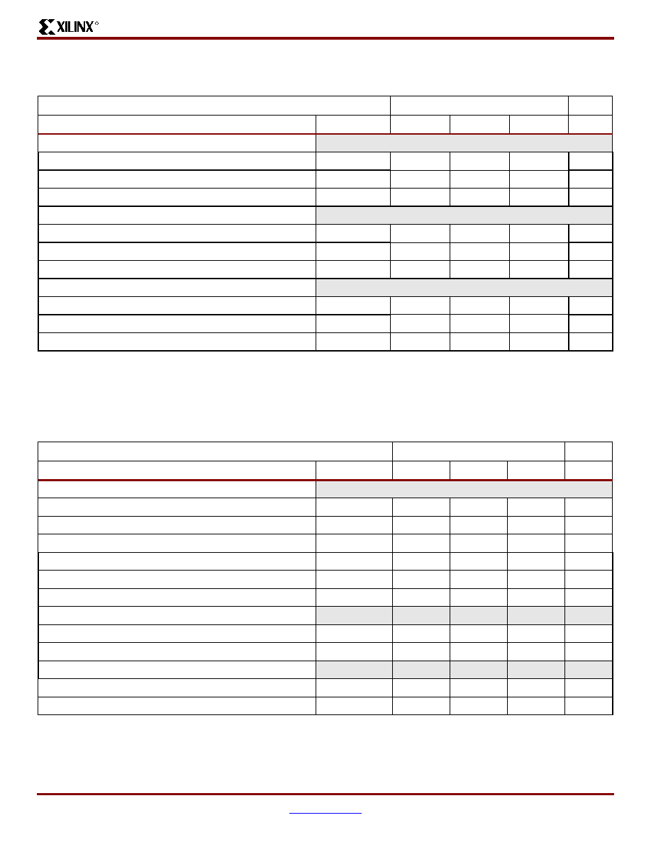
Virtex-II ProTM Platform FPGAs: DC and Switching Characteristics
R
DS083-3 (v2.12) November 11, 2003
www.xilinx.com
31
Advance Product Specification
1-800-255-7778
CLB Distributed RAM Switching Characteristics
CLB Shift Register Switching Characteristics
Table 34: CLB Distributed RAM Switching Characteristics
Speed
Grade
Description
Symbol
-
7
-
6 -5
Units
Sequential Delays
Clock CLK to X/Y outputs (WE active) in 16 x 1 mode
T
SHCKO16
1.25
1.38
1.54
ns, max
Clock CLK to X/Y outputs (WE active) in 32 x 1 mode
T
SHCKO32
1.57
1.75
1.95
ns, max
Clock CLK to F5 output
T
SHCKOF5
1.52
1.68
1.88
ns, max
Setup and Hold Times Before/After Clock CLK
BX/BY data inputs (DIN)
T
DS
/T
DH
0.38/≠0.07
0.41/≠0.07
0.46/≠0.08
ns, min
F/G address inputs
T
AS
/T
AH
0.42/ 0.00
0.47/ 0.00
0.52/ 0.00
ns, min
SR input
T
WES
/T
WEH
0.22/ 0.04
0.24/ 0.05
0.26/ 0.05
ns, min
Clock CLK
Minimum Pulse Width, High
T
WPH
0.63
0.72
0.79
ns, min
Minimum Pulse Width, Low
T
WPL
0.63
0.72
0.79
ns, min
Minimum clock period to meet address write cycle time
T
WC
1.25
1.44
1.58
ns, min
Notes:
1.
A Zero "0" Hold Time listing indicates no hold time or a negative hold time. Negative values cannot be guaranteed "best-case", but if
a "0" is listed, there is no positive hold time.
Table 35: CLB Shift Register Switching Characteristics
Speed
Grade
Description
Symbol
-7
-6
-5
Units
Sequential Delays
Clock CLK to X/Y outputs
T
REG
2.78
3.12
3.49
ns, max
Clock CLK to X/Y outputs
T
REG32
3.10
3.49
3.90
ns, max
Clock CLK to XB output via MC15 LUT output
T
REGXB
2.84
3.18
3.55
ns, max
Clock CLK to YB output via MC15 LUT output
T
REGYB
2.55
2.88
3.21
ns, max
Clock CLK to Shiftout
T
CKSH
2.50
2.83
3.15
ns, max
Clock CLK to F5 output
T
REGF5
3.05
3.42
3.83
ns, max
Setup and Hold Times Before/After Clock CLK
BX/BY data inputs (DIN)
T
SRLDS
/T
SRLDH
0.70/≠0.16
0.77/≠0.18
0.98/≠0.21
ns, min
SR input
T
WSS
/T
WSH
0.27/ 0.01
0.34/ 0.01
0.47/ 0.01
ns, min
Clock CLK
Minimum Pulse Width, High
T
SRPH
0.63
0.72
0.79
ns, min
Minimum Pulse Width, Low
T
SRPL
0.63
0.72
0.79
ns, min
Notes:
1.
A Zero "0" Hold Time listing indicates no hold time or a negative hold time. Negative values cannot be guaranteed "best-case", but if
a "0" is listed, there is no positive hold time.
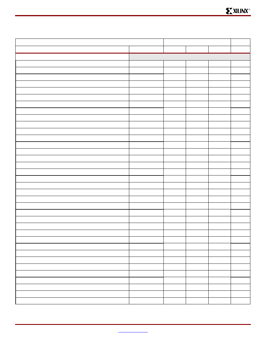
Virtex-II Pro Switching Characteristics
R
32
www.xilinx.com
DS083-3 (v2.12) November 11, 2003
1-800-255-7778
Advance Product Specification
Multiplier Switching Characteristics
Table 36: Multiplier Switching Characteristics
Speed Grade
Description
Symbol
-7
-6
-5
Units
Propagation Delay to Output Pin
Input to Pin35
T
MULT_P35
4.08
4.64
5.19
ns, max
Input to Pin34
T
MULT_P34
3.99
4.55
5.09
ns, max
Input to Pin33
T
MULT_P33
3.90
4.45
4.99
ns, max
Input to Pin32
T
MULT_P32
3.80
4.36
4.88
ns, max
Input to Pin31
T
MULT_P31
3.71
4.27
4.78
ns, max
Input to Pin30
T
MULT_P30
3.62
4.17
4.67
ns, max
Input to Pin29
T
MULT_P29
3.53
4.08
4.57
ns, max
Input to Pin28
T
MULT_P28
3.43
3.99
4.46
ns, max
Input to Pin27
T
MULT_P27
3.34
3.89
4.36
ns, max
Input to Pin26
T
MULT_P26
3.25
3.80
4.26
ns, max
Input to Pin25
T
MULT_P25
3.16
3.71
4.15
ns, max
Input to Pin24
T
MULT_P24
3.06
3.61
4.05
ns, max
Input to Pin23
T
MULT_P23
2.97
3.52
3.94
ns, max
Input to Pin22
T
MULT_P22
2.88
3.43
3.84
ns, max
Input to Pin21
T
MULT_P21
2.79
3.34
3.73
ns, max
Input to Pin20
T
MULT_P20
2.70
3.24
3.63
ns, max
Input to Pin19
T
MULT_P19
2.60
3.15
3.53
ns, max
Input to Pin18
T
MULT_P18
2.51
3.06
3.42
ns, max
Input to Pin17
T
MULT_P17
2.42
2.96
3.32
ns, max
Input to Pin16
T
MULT_P16
2.34
2.86
3.21
ns, max
Input to Pin15
T
MULT_P15
2.27
2.76
3.09
ns, max
Input to Pin14
T
MULT_P14
2.19
2.67
2.98
ns, max
Input to Pin13
T
MULT_P13
2.12
2.57
2.87
ns, max
Input to Pin12
T
MULT_P12
2.04
2.47
2.76
ns, max
Input to Pin11
T
MULT_P11
1.96
2.37
2.65
ns, max
Input to Pin10
T
MULT_P10
1.89
2.27
2.54
ns, max
Input to Pin9
T
MULT_P9
1.81
2.17
2.43
ns, max
Input to Pin8
T
MULT_P8
1.74
2.07
2.32
ns, max
Input to Pin7
T
MULT_P7
1.66
1.97
2.21
ns, max
Input to Pin6
T
MULT_P6
1.59
1.87
2.09
ns, max
Input to Pin5
T
MULT_P5
1.51
1.77
1.98
ns, max
Input to Pin4
T
MULT_P4
1.44
1.67
1.87
ns, max
Input to Pin3
T
MULT_P3
1.36
1.57
1.76
ns, max
Input to Pin2
T
MULT_P2
1.28
1.47
1.65
ns, max
Input to Pin1
T
MULT_P1
1.21
1.37
1.54
ns, max
Input to Pin0
T
MULT_P0
1.13
1.27
1.43
ns, max
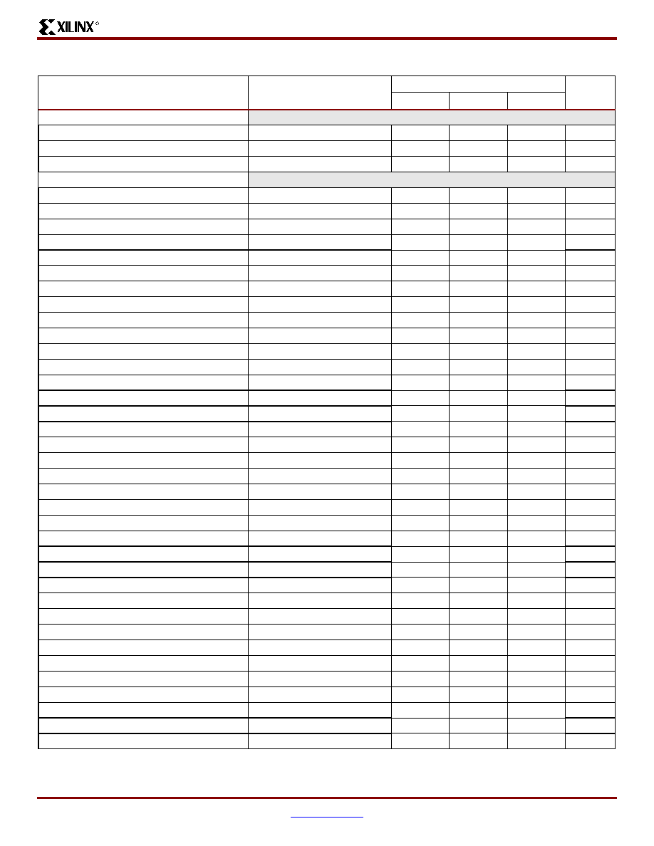
Virtex-II ProTM Platform FPGAs: DC and Switching Characteristics
R
DS083-3 (v2.12) November 11, 2003
www.xilinx.com
33
Advance Product Specification
1-800-255-7778
Table 37: Pipelined Multiplier Switching Characteristics
Description
Symbol
Speed Grade
Units
-7 -6 -5
Setup and Hold Times Before/After Clock
Data Inputs
T
MULIDCK
/T
MULCKID
1.86/ 0.00
2.06/ 0.00
2.31/ 0.00
ns, max
Clock Enable
T
MULIDCK_CE
/T
MULCKID_CE
0.23/ 0.00
0.25/ 0.00
0.28/ 0.00
ns, max
Reset
T
MULIDCK_RST
/T
MULCKID_RST
0.21/≠0.09
0.24/≠0.09
0.26/≠0.10
ns, max
Clock to Output Pin
Clock to Pin35
T
MULTCK_P35
2.45
2.92
3.27
ns, max
Clock to Pin34
T
MULTCK_P34
2.36
2.82
3.16
ns, max
Clock to Pin33
T
MULTCK_P33
2.28
2.72
3.05
ns, max
Clock to Pin32
T
MULTCK_P32
2.20
2.62
2.93
ns, max
Clock to Pin31
T
MULTCK_P31
2.12
2.52
2.82
ns, max
Clock to Pin30
T
MULTCK_P30
2.03
2.42
2.71
ns, max
Clock to Pin29
T
MULTCK_P29
1.95
2.32
2.60
ns, max
Clock to Pin28
T
MULTCK_P28
1.87
2.22
2.48
ns, max
Clock to Pin27
T
MULTCK_P27
1.79
2.12
2.37
ns, max
Clock to Pin26
T
MULTCK_P26
1.70
2.02
2.26
ns, max
Clock to Pin25
T
MULTCK_P25
1.62
1.92
2.15
ns, max
Clock to Pin24
T
MULTCK_P24
1.54
1.82
2.03
ns, max
Clock to Pin23
T
MULTCK_P23
1.46
1.71
1.92
ns, max
Clock to Pin22
T
MULTCK_P22
1.37
1.61
1.81
ns, max
Clock to Pin21
T
MULTCK_P21
1.29
1.51
1.69
ns, max
Clock to Pin20
T
MULTCK_P20
1.21
1.41
1.58
ns, max
Clock to Pin19
T
MULTCK_P19
1.13
1.31
1.47
ns, max
Clock to Pin18
T
MULTCK_P18
1.04
1.21
1.36
ns, max
Clock to Pin17
T
MULTCK_P17
0.96
1.11
1.24
ns, max
Clock to Pin16
T
MULTCK_P16
0.88
1.01
1.13
ns, max
Clock to Pin15
T
MULTCK_P15
0.80
0.91
1.02
ns, max
Clock to Pin14
T
MULTCK_P14
0.71
0.81
0.91
ns, max
Clock to Pin13
T
MULTCK_P13
0.63
0.71
0.79
ns, max
Clock to Pin12
T
MULTCK_P12
0.63
0.71
0.79
ns, max
Clock to Pin11
T
MULTCK_P11
0.63
0.71
0.79
ns, max
Clock to Pin10
T
MULTCK_P10
0.63
0.71
0.79
ns, max
Clock to Pin9
T
MULTCK_P9
0.63
0.71
0.79
ns, max
Clock to Pin8
T
MULTCK_P8
0.63
0.71
0.79
ns, max
Clock to Pin7
T
MULTCK_P7
0.63
0.71
0.79
ns, max
Clock to Pin6
T
MULTCK_P6
0.63
0.71
0.79
ns, max
Clock to Pin5
T
MULTCK_P5
0.63
0.71
0.79
ns, max
Clock to Pin4
T
MULTCK_P4
0.63
0.71
0.79
ns, max
Clock to Pin3
T
MULTCK_P3
0.63
0.71
0.79
ns, max
Clock to Pin2
T
MULTCK_P2
0.63
0.71
0.79
ns, max
Clock to Pin1
T
MULTCK_P1
0.63
0.71
0.79
ns, max
Clock to Pin0
T
MULTCK_P0
0.63
0.71
0.79
ns, max
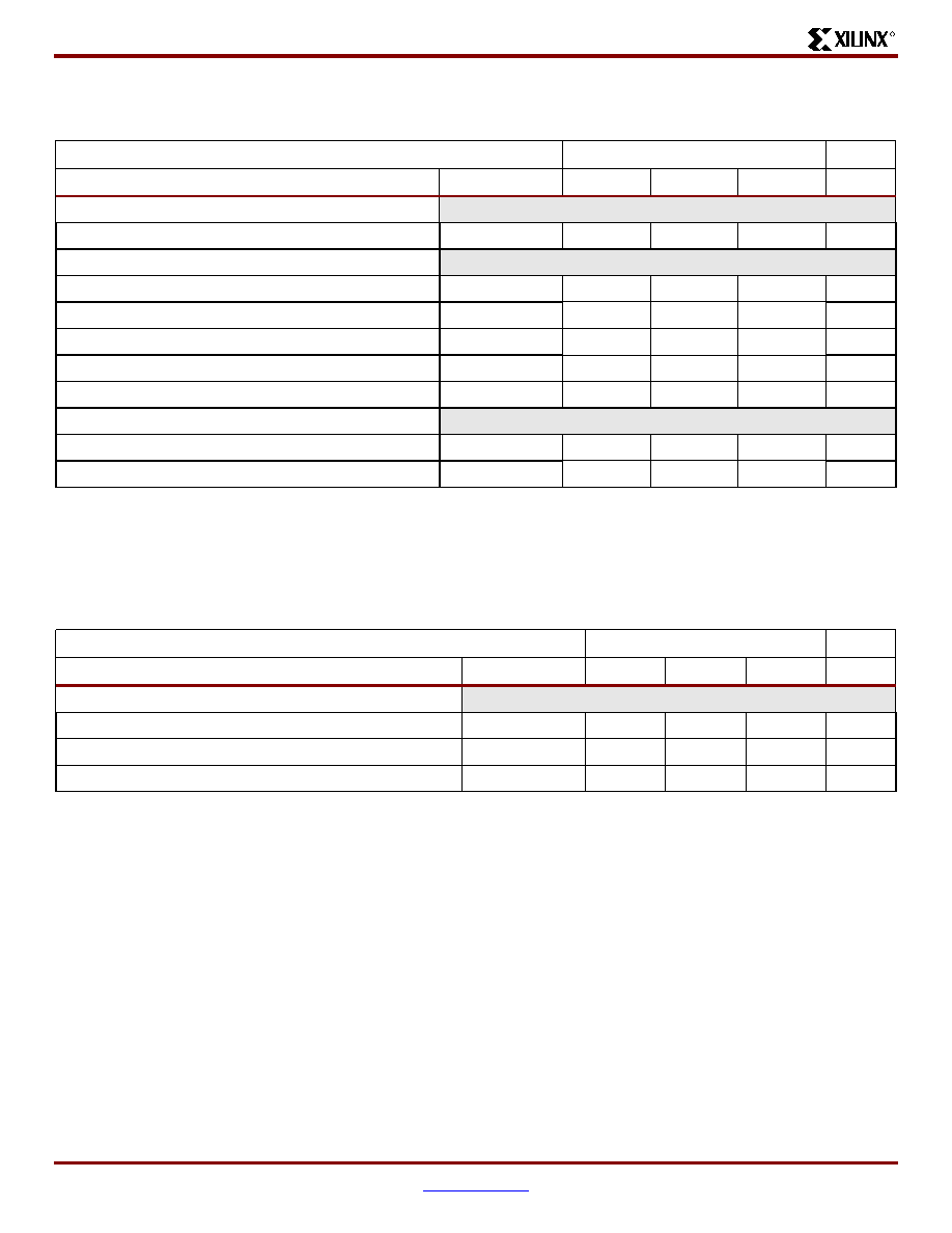
Virtex-II Pro Switching Characteristics
R
34
www.xilinx.com
DS083-3 (v2.12) November 11, 2003
1-800-255-7778
Advance Product Specification
Block SelectRAM+ Switching Characteristics
TBUF Switching Characteristics
Table 38: Block SelectRAM+ Switching Characteristics
Speed Grade
Description
Symbol
-7
-6
-5
Units
Sequential Delays
Clock CLK to DOUT output
T
BCKO
1.41
1.50
1.68
ns, max
Setup and Hold Times Before Clock CLK
ADDR inputs
T
BACK
/T
BCKA
0.27/ 0.22
0.31/ 0.25
0.35/ 0.28
ns, min
DIN inputs
T
BDCK
/T
BCKD
0.20/ 0.22
0.23/ 0.25
0.26/ 0.28
ns, min
EN input
T
BECK
/T
BCKE
0.28/ 0.00
0.32/ 0.00
0.35/ 0.00
ns, min
RST input
T
BRCK
/T
BCKR
0.28/ 0.00
0.32/ 0.00
0.35/ 0.00
ns, min
WEN input
T
BWCK
/T
BCKW
0.33/ 0.00
0.35/ 0.00
0.39/ 0.00
ns, min
Clock CLK
Minimum Pulse Width, High
T
BPWH
1.17
1.30
1.50
ns, min
Minimum Pulse Width, Low
T
BPWL
1.17
1.30
1.50
ns, min
Notes:
1.
A Zero "0" Hold Time listing indicates no hold time or a negative hold time. Negative values can not be guaranteed "best-case", but
if a "0" is listed, there is no positive hold time.
Table 39: TBUF Switching Characteristics
Speed Grade
Description
Symbol
-7
-6
-5
Units
Combinatorial Delays
IN input to OUT output
T
IO
0.88
1.01
1.12
ns, max
TRI input to OUT output high-impedance
T
OFF
0.48
0.55
0.61
ns, max
TRI input to valid data on OUT output
T
ON
0.48
0.55
0.61
ns, max
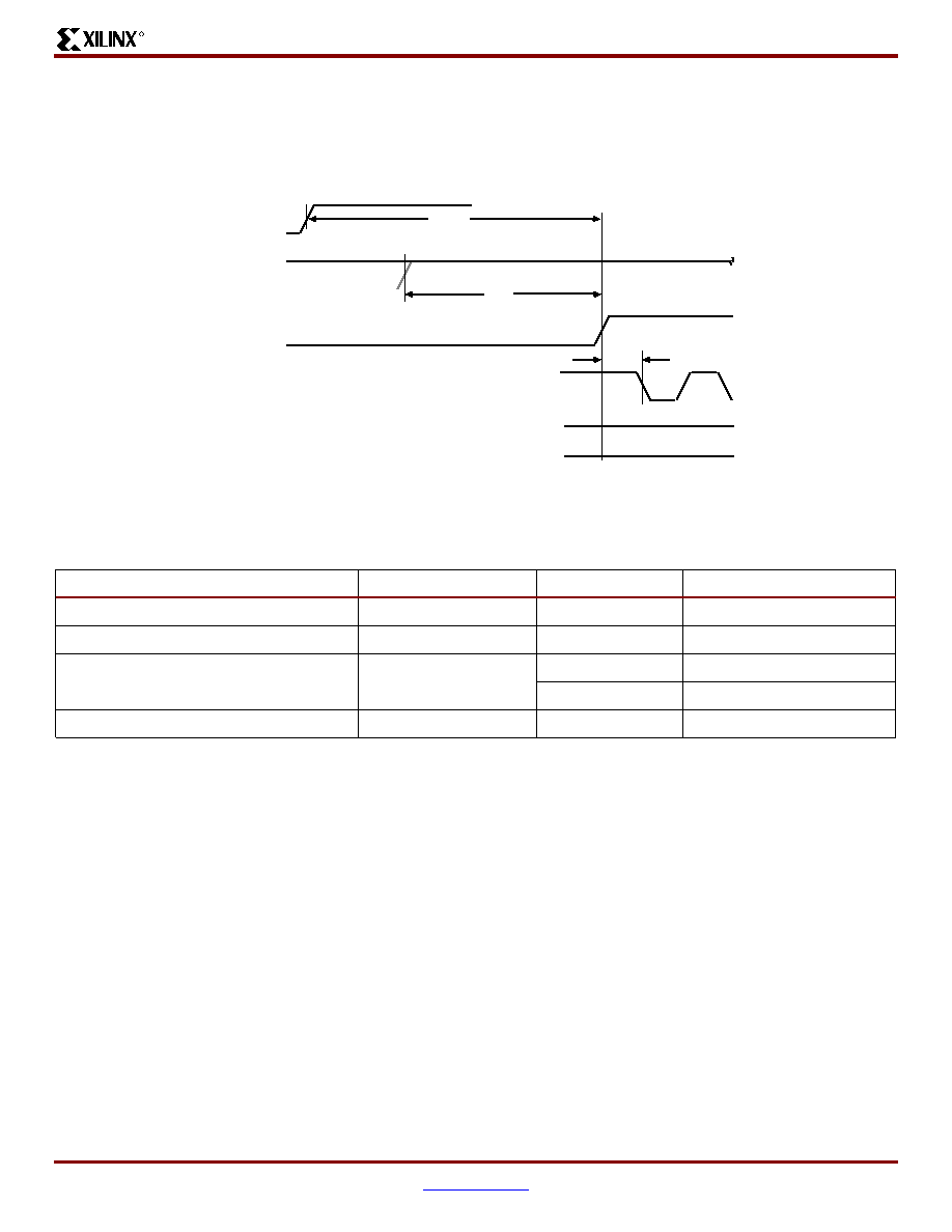
Virtex-II ProTM Platform FPGAs: DC and Switching Characteristics
R
DS083-3 (v2.12) November 11, 2003
www.xilinx.com
35
Advance Product Specification
1-800-255-7778
Configuration Timing
Configuration Memory Clearing Parameters
Power-up timing of configuration signals is shown in
Figure 7
; corresponding timing characteristics are listed in
Table 40
.
Figure 7: Power-Up Timing Configuration Signals
PROG_B
Vcc
CCLK OUTPUT or INPUT
M0, M1, M2*
(Required)
T
PL
T
ICCK
ds083-3_07_091003
T
POR
INIT_B
*Can be either 0 or 1, but must not toggle during and after configuration.
Table 40: Power-Up Timing Characteristics
Description
Symbol
Value
Units
Program Latency
T
PL
4
µ
s per frame, max
Power-on-Reset
T
POR
T
PL
+ 2
ms, max
CCLK (output) Delay
T
ICCK
µ
s, min
µ
s, max
Program Pulse Width
T
PROGRAM
300
ns, min
Notes:
1.
The M2, M1, and M0 mode pins should be set at a constant DC voltage level, either through pullup or pulldown resistors, or tied
directly to ground or V
CCAUX
. The mode pins should not be toggled during and after configuration.
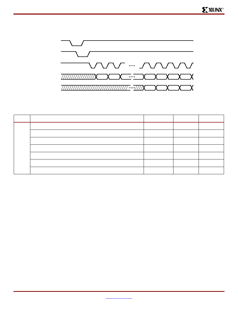
Virtex-II Pro Switching Characteristics
R
36
www.xilinx.com
DS083-3 (v2.12) November 11, 2003
1-800-255-7778
Advance Product Specification
Master/Slave Serial Mode Parameters
For Slave configurations, a free running CCLK can be used, as shown in
Figure 8
.
.
Figure 8: Serial Configuration Clocking Sequence
PROG_B
INIT_B
CCLK
DIN
ug002_c3_028_112900
BIT 0
BIT 1
BIT n
BIT n+1
BIT n-63
BIT n-64
DOUT
Table 41: Master/Slave Serial Mode Programming Switching
Description
Symbol
Values
Units
CCLK
DIN setup/hold, slave mode
T
DCC
/T
CCD
5.0/0.0
ns, min
DIN setup/hold, master mode
T
DSCK
/T
SCKD
5.0/0.0
ns, min
DOUT
T
CCO
12.0
ns, max
High time
T
CCH
5.0
ns, min
Low time
T
CCL
5.0
ns, min
Maximum Frequency
F
CC_SERIAL
66
MHz, max
Frequency Tolerance, master mode with respect to nominal
+45% -30%

Virtex-II ProTM Platform FPGAs: DC and Switching Characteristics
R
DS083-3 (v2.12) November 11, 2003
www.xilinx.com
37
Advance Product Specification
1-800-255-7778
Master/Slave SelectMAP Parameters
Figure 9
is a generic diagram for data loading using SelectMAP. For other data loading diagrams, refer to the Virtex-II Pro
Platform FPGA User Guide.
Figure 9: Data Loading in SelectMAP
PROGRAM
INIT
CCLK
CS
WRITE
DATA[0:7]
x138_06_022400
Byte 0
Byte 1
Byte n
Byte n
Byte n
Loaded
Byte n
Ignored
Byte 0
Loaded
Device
Ready
BUSY
Byte n+1
BUSY
Table 42: SelectMAP Write Timing Characteristics
Description
Symbol
Value
Units
CCLK
D
0-7
Setup/Hold T
SMDCC
/T
SMCCD
5.0/0.0
ns, min
CS_B Setup/Hold
T
SMCSCC
/T
SMCCCS
7.0/0.0
ns, min
RDWR_B Setup/Hold
T
SMCCW
/T
SMWCC
7.0/0.0
ns, min
BUSY Propagation Delay
T
SMCKBY
12.0
ns, max
Maximum Frequency
F
CC_
SelectMAP
50
MHz, max
Maximum Frequency with No Handshake
F
CCNH
50
MHz, max

Virtex-II Pro Switching Characteristics
R
38
www.xilinx.com
DS083-3 (v2.12) November 11, 2003
1-800-255-7778
Advance Product Specification
JTAG Test Access Port Switching Characteristics
Characterization data for some of the most commonly requested timing parameters shown in
Figure 10
is listed in
Table 43
.
Figure 10: Virtex-II Pro Boundary Scan Port Timing Waveforms
Table 43: Boundary-Scan Port Timing Specifications
Symbol
Parameter
Value
Units
T
TAPTCK
TMS and TDI setup time before TCK
5.5
ns, min
T
TCKTAP
TMS and TDI hold times after TCK
2.0
ns, min
T
TCKTDO
TCK falling edge to TDO output valid
11.0
ns, min
F
TCK
Maximum TCK clock frequency
33.0
MHz, max
x139_05_020300
Data to be captured
Data to be driven out
TDO
TCK
TDI
TMS
Data Valid
Data Valid
T
TCKTDO
T
TAPTCK
T
TCKTAP
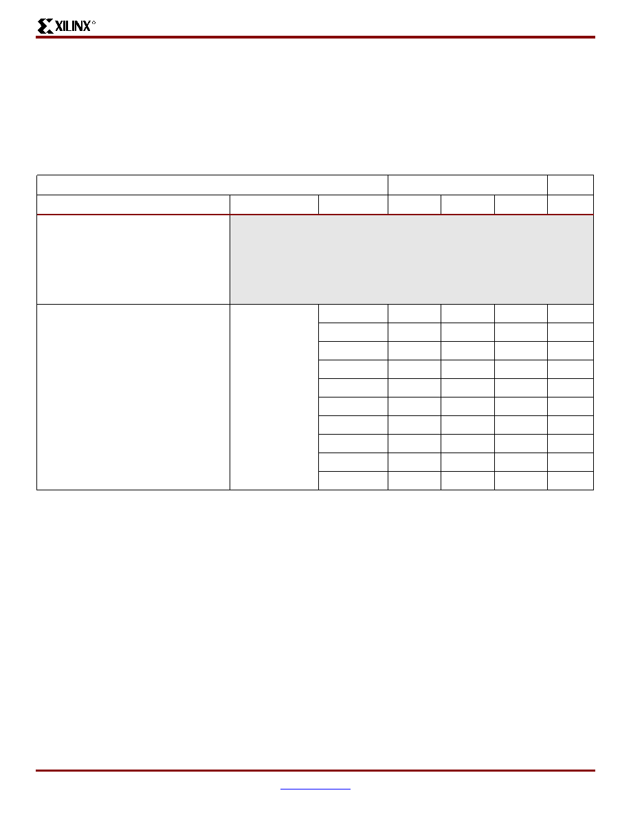
Virtex-II ProTM Platform FPGAs: DC and Switching Characteristics
R
DS083-3 (v2.12) November 11, 2003
www.xilinx.com
39
Advance Product Specification
1-800-255-7778
Virtex-II Pro Pin-to-Pin Output Parameter Guidelines
All devices are 100% functionally tested. Listed below are representative values for typical pin locations and normal clock
loading. Values are expressed in nanoseconds unless otherwise noted.
Global Clock Input to Output Delay for LVCMOS25, 12 mA, Fast Slew Rate,
With DCM
Table 44: Global Clock Input to Output Delay for LVCMOS25, 12 mA, Fast Slew Rate,
With DCM
Speed Grade
Description
Symbol
Device
-7
-6
-5
Units
LVCMOS25 Global Clock Input to Output
Delay using Output Flip-flop, 12 mA, Fast
Slew Rate, with DCM.
For data output with different standards,
adjust the delays with the values shown in
IOB Output Switching Characteristics
Standard Adjustments
, page 25
.
Global Clock and OFF with DCM
T
ICKOFDCM
XC2VP2
2.40
2.50
ns
XC2VP4
2.40
2.50
ns
XC2VP7
2.40
2.50
ns
XC2VP20
2.40
2.50
ns
XC2VP30
2.50
2.60
ns
XC2VP40
2.60
2.70
ns
XC2VP50
2.70
2.80
ns
XC2VP70
2.80
2.90
ns
XC2VP100
ns
XC2VP125
ns
Notes:
1.
Listed above are representative values where one global clock input drives one vertical clock line in each accessible column, and
where all accessible IOB and CLB flip-flops are clocked by the global clock net.
2.
Output timing is measured at 50% V
CC
threshold with test setup shown in
Figure 6
. For other I/O standards, see
Table 32
.
3.
DCM output jitter is already included in the timing calculation.

Virtex-II Pro Pin-to-Pin Output Parameter Guidelines
R
40
www.xilinx.com
DS083-3 (v2.12) November 11, 2003
1-800-255-7778
Advance Product Specification
Global Clock Input to Output Delay for LVCMOS25, 12 mA, Fast Slew Rate,
Without DCM
Table 45: Global Clock Input to Output Delay for LVCMOS25, 12 mA, Fast Slew Rate,
Without DCM
Speed Grade
Description
Symbol
Device
-7
-6
-5
Units
LVCMOS25 Global Clock Input to Output
Delay using Output Flip-flop, 12 mA, Fast
Slew Rate, without DCM.
For data output with different standards,
adjust the delays with the values shown in
IOB Output Switching Characteristics
Standard Adjustments
, page 25
.
Global Clock and OFF without DCM
T
ICKOF
XC2VP2
4.80
5.26
ns
XC2VP4
4.80
5.26
ns
XC2VP7
4.80
5.26
ns
XC2VP20
4.90
5.31
ns
XC2VP30
5.00
5.40
ns
XC2VP40
5.10
5.50
ns
XC2VP50
5.20
5.60
ns
XC2VP70
5.60
6.10
ns
XC2VP100
ns
XC2VP125
ns
Notes:
1.
Listed above are representative values where one global clock input drives one vertical clock line in each accessible column, and
where all accessible IOB and CLB flip-flops are clocked by the global clock net.
2.
Output timing is measured at 50% V
CC
threshold with test setup shown in
Figure 6
. For other I/O standards, see
Table 32
.
3.
DCM output jitter is already included in the timing calculation.
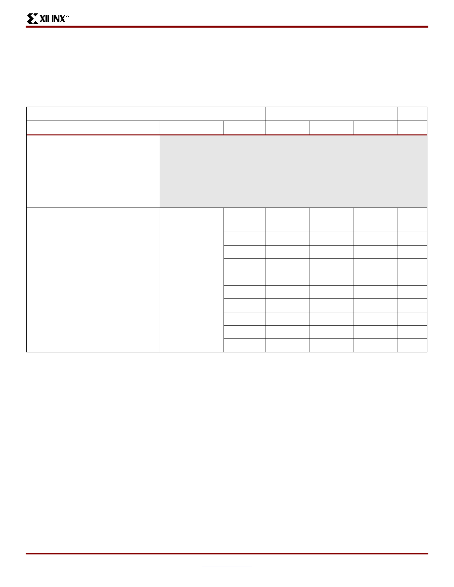
Virtex-II ProTM Platform FPGAs: DC and Switching Characteristics
R
DS083-3 (v2.12) November 11, 2003
www.xilinx.com
41
Advance Product Specification
1-800-255-7778
Virtex-II Pro Pin-to-Pin Input Parameter Guidelines
All devices are 100% functionally tested. Listed below are representative values for typical pin locations and normal clock
loading. Values are expressed in nanoseconds unless otherwise noted
Global Clock Set-Up and Hold for LVCMOS25 Standard, With DCM
Table 46: Global Clock Set-Up and Hold for LVCMOS25 Standard, With DCM
Speed Grade
Description
Symbol
Device
-7
-6
-5
Units
Input Setup and Hold Time Relative to
Global Clock Input Signal for LVCMOS25
Standard.
For data input with different standards,
adjust the setup time delay by the values
shown in IOB Input Switching
Characteristics Standard Adjustments
,
page 22
.
No Delay
Global Clock and IFF with DCM
T
PSDCM
/T
PHDCM
XC2VP2
ns
XC2VP4
ns
XC2VP7
ns
XC2VP20
ns
XC2VP30
ns
XC2VP40
ns
XC2VP50
ns
XC2VP70
ns
XC2VP100
ns
XC2VP125
ns
Notes:
1.
IFF = Input Flip-Flop or Latch
2.
Setup time is measured relative to the Global Clock input signal with the fastest route and the lightest load. Hold time is measured
relative to the Global Clock input signal with the slowest route and heaviest load.
3.
DCM output jitter is already included in the timing calculation.
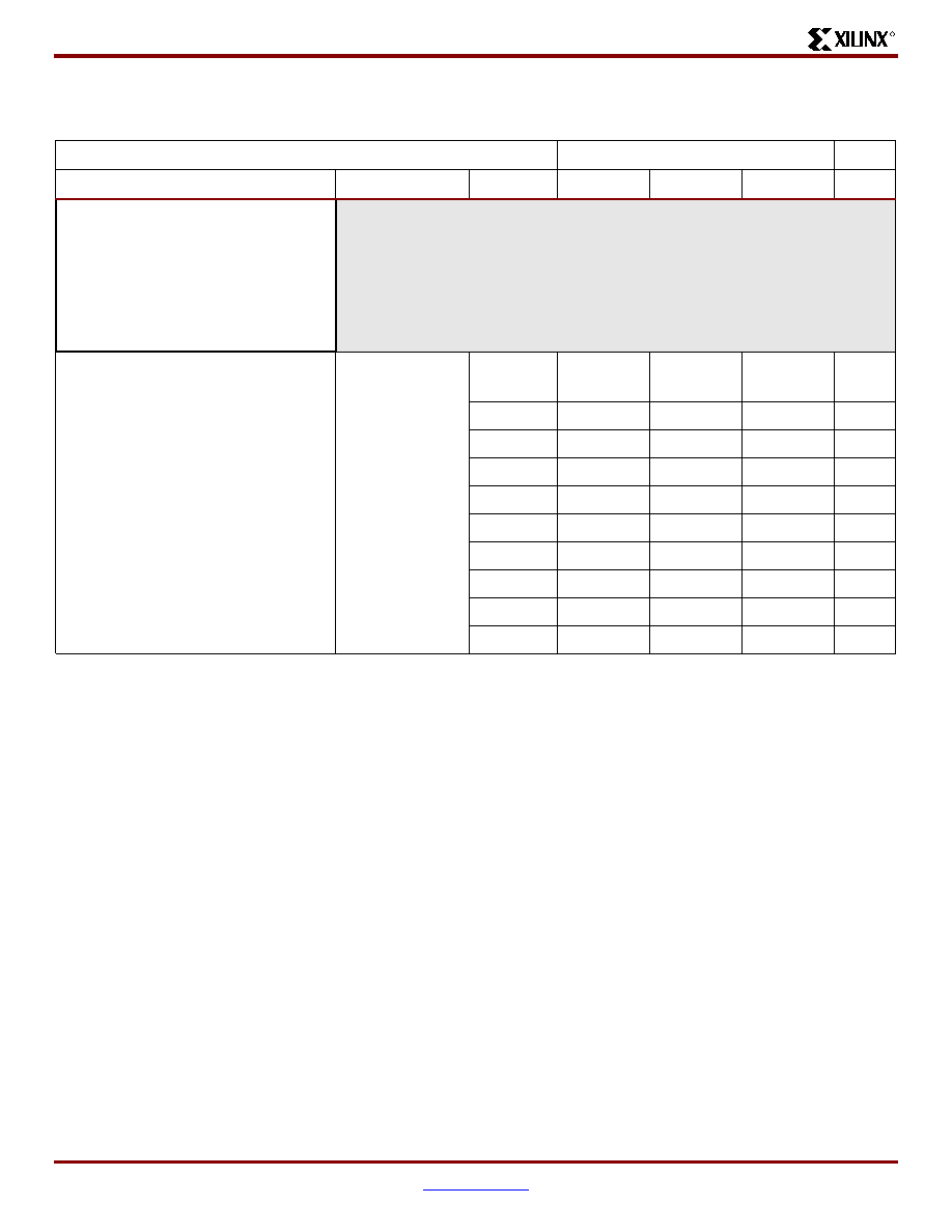
Virtex-II Pro Pin-to-Pin Input Parameter Guidelines
R
42
www.xilinx.com
DS083-3 (v2.12) November 11, 2003
1-800-255-7778
Advance Product Specification
Global Clock Set-Up and Hold for LVCMOS25 Standard, Without DCM
,
Table 47: Global Clock Set-Up and Hold for LVCMOS25 Standard, Without DCM
Speed Grade
Description
Symbol
Device
-7
-6
-5
Units
Input Setup and Hold Time Relative to
Global Clock Input Signal for LVCMOS25
Standard.
For data input with different standards,
adjust the setup time delay by the values
shown in IOB Input Switching
Characteristics Standard Adjustments
,
page 22
.
Full Delay
Global Clock and IFF without DCM
T
PSFD
/T
PHFD
XC2VP2
1.92/ 0.00
1.92/ 0.00
ns
XC2VP4
1.92/ 0.00
1.92/ 0.00
ns
XC2VP7
1.92/ 0.00
1.92/ 0.00
ns
XC2VP20
1.92/ 0.00
1.92/ 0.00
ns
XC2VP30
2.00/ 0.00
2.00/ 0.00
ns
XC2VP40
2.70/≠0.39
2.70/≠0.39
ns
XC2VP50
3.00/≠0.70
3.00/≠0.70
ns
XC2VP70
2.80/≠0.15
2.80/≠0.15
ns
XC2VP100
ns
XC2VP125
ns
Notes:
1.
IFF = Input Flip-Flop or Latch
2.
Setup time is measured relative to the Global Clock input signal with the fastest route and the lightest load. Hold time is measured
relative to the Global Clock input signal with the slowest route and heaviest load.
3.
A Zero "0" Hold Time listing indicates no hold time or a negative hold time. Negative values can not be guaranteed "best-case", but
if a "0" is listed, there is no positive hold time.
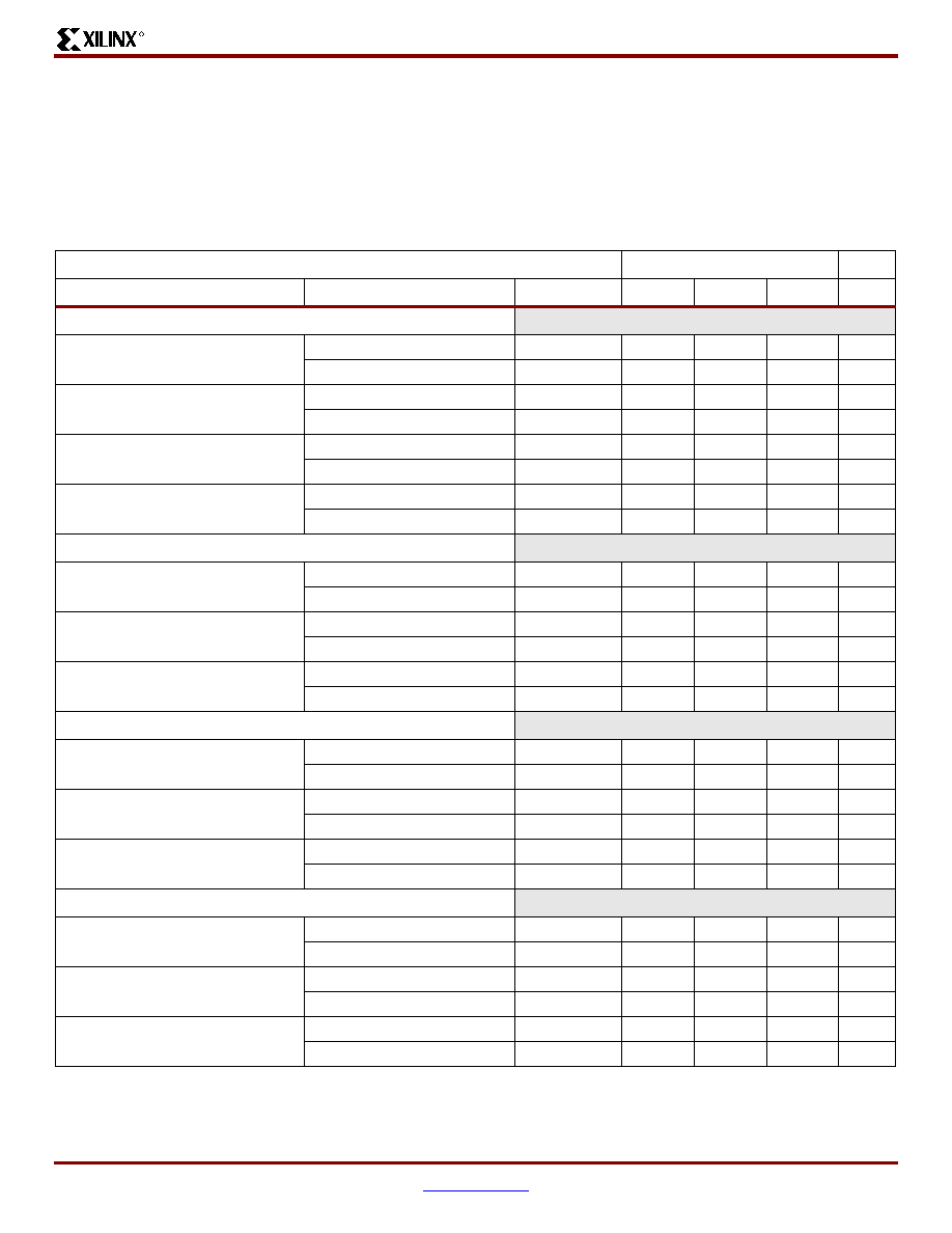
Virtex-II ProTM Platform FPGAs: DC and Switching Characteristics
R
DS083-3 (v2.12) November 11, 2003
www.xilinx.com
43
Advance Product Specification
1-800-255-7778
DCM Timing Parameters
All devices are 100% functionally tested. Because of the dif-
ficulty in directly measuring many internal timing parame-
ters, those parameters are derived from benchmark timing
patterns. The following guidelines reflect worst-case values
across the recommended operating conditions. All output
jitter and phase specifications are determined through sta-
tistical measurement at the package pins.
Operating Frequency Ranges
e
Table 48: Operating Frequency Ranges
Speed Grade
Description
Symbol
Constraints
-7
-6
-5
Units
Output Clocks (Low Frequency Mode)
CLK0, CLK90, CLK180, CLK270
CLKOUT_FREQ_1X_LF_MIN
24.00
24.00
MHz
CLKOUT_FREQ_1X_LF_MAX
210.00
180.00
MHz
CLK2X, CLK2X180
CLKOUT_FREQ_2X_LF_MIN
48.00
48.00
MHz
CLKOUT_FREQ_2X_LF_MAX
420.00
360.00
MHz
CLKDV
CLKOUT_FREQ_DV_LF_MIN
1.50
1.50
MHz
CLKOUT_FREQ_DV_LF_MAX
140.00
120.00
MHz
CLKFX, CLKFX180
CLKOUT_FREQ_FX_LF_MIN
24.00
24.00
MHz
CLKOUT_FREQ_FX_LF_MAX
240.00
210.00
MHz
Input Clocks (Low Frequency Mode)
CLKIN (using DLL outputs)
(1)
CLKIN_FREQ_DLL_LF_MIN
24.00
24.00
MHz
CLKIN_FREQ_DLL_LF_MAX
210.00
180.00
MHz
CLKIN (using CLKFX outputs)
(2)
CLKIN_FREQ_FX_LF_MIN
1.00
1.00
MHz
CLKIN_FREQ_FX_LF_MAX
240.00
210.00
MHz
PSCLK
PSCLK_FREQ_LF_MIN
0.01
0.01
MHz
PSCLK_FREQ_LF_MAX
420.00
360.00
MHz
Output Clocks (High Frequency Mode)
CLK0, CLK180
CLKOUT_FREQ_1X_HF_MIN
48.00
48.00
MHz
CLKOUT_FREQ_1X_HF_MAX
420.00
360.00
MHz
CLKDV
CLKOUT_FREQ_DV_HF_MIN
3.00
3.00
MHz
CLKOUT_FREQ_DV_HF_MAX
280.00
240.00
MHz
CLKFX, CLKFX180
CLKOUT_FREQ_FX_HF_MIN
210.00
210.00
MHz
CLKOUT_FREQ_FX_HF_MAX
320.00
270.00
MHz
Input Clocks (High Frequency Mode)
CLKIN (using DLL outputs)
(1)
CLKIN_FREQ_DLL_HF_MIN
48.00
48.00
MHz
CLKIN_FREQ_DLL_HF_MAX
420.00
360.00
MHz
CLKIN (using CLKFX outputs)
(2)
CLKIN_FREQ_FX_HF_MIN
50.00
50.00
MHz
CLKIN_FREQ_FX_HF_MAX
320.00
270.00
MHz
PSCLK
PSCLK_FREQ_HF_MIN
0.01
0.01
MHz
PSCLK_FREQ_HF_MAX
420.00
360.00
MHz
Notes:
1.
"DLL outputs" is used here to describe the outputs: CLK0, CLK90, CLK180, CLK270, CLK2X, CLK2X180, and CLKDV.
2.
If both DLL and CLKFX outputs are used, follow the more restrictive specification.
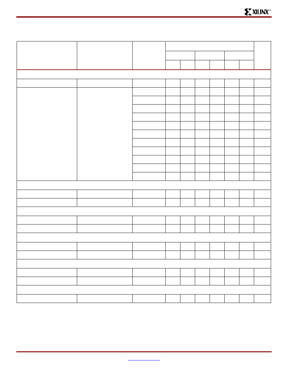
DCM Timing Parameters
R
44
www.xilinx.com
DS083-3 (v2.12) November 11, 2003
1-800-255-7778
Advance Product Specification
Input Clock Tolerances
Table 49: Input Clock Tolerances
Description
Symbol
Constraints
F
CLKIN
Speed Grade
Units
≠7
≠6
≠5
Min
Max
Min
Max
Min
Max
Input Clock Low/High Pulse Width
PSCLK
PSCLK_PULSE
< 1MHz
25.00
25.00
ns
PSCLK and CLKIN
(3)
PSCLK_PULSE and
CLKIN_PULSE
1 ≠ 10 MHz
25.00
25.00
ns
10 ≠ 25 MHz
10.00
10.00
ns
25 ≠ 50 MHz
5.00
5.00
ns
50 ≠ 100 MHz
3.00
3.00
ns
100 ≠ 150 MHz
2.40
2.40
ns
150 ≠ 200 MHz
2.00
2.00
ns
200 ≠ 250 MHz
1.80
1.80
ns
250 ≠ 300 MHz
1.50
1.50
ns
300 ≠ 350 MHz
1.30
1.30
ns
350 ≠ 400 MHz
1.15
1.15
ns
> 400 MHz
1.05
1.05
ns
Input Clock Cycle-Cycle Jitter (Low Frequency Mode)
CLKIN (using DLL outputs)
(1)
CLKIN_CYC_JITT_DLL_LF
±300
±300
ps
CLKIN (using CLKFX outputs)
(2)
CLKIN_CYC_JITT_FX_LF
±300
±300
ps
Input Clock Cycle-Cycle Jitter (High Frequency Mode)
CLKIN (using DLL outputs)
(1)
CLKIN_CYC_JITT_DLL_HF
±150
±150
ps
CLKIN (using CLKFX outputs)
(2)
CLKIN_CYC_JITT_FX_HF
±150
±150
ps
Input Clock Period Jitter (Low Frequency Mode)
CLKIN (using DLL outputs)
(1)
CLKIN_PER_JITT_DLL_LF
±1
±1
ns
CLKIN (using CLKFX outputs)
(2)
CLKIN_PER_JITT_FX_LF
±1
±1
ns
Input Clock Period Jitter (High Frequency Mode)
CLKIN (using DLL outputs)
(1)
CLKIN_PER_JITT_DLL_HF
±1
±1
ns
CLKIN (using CLKFX outputs)
(2)
CLKIN_PER_JITT_FX_HF
±1
±1
ns
Feedback Clock Path Delay Variation
CLKFB off-chip feedback
CLKFB_DELAY_VAR_EXT
±1
±1
ns
Notes:
1.
"DLL outputs" is used here to describe the outputs: CLK0, CLK90, CLK180, CLK270, CLK2X, CLK2X180, and CLKDV.
2.
If both DLL and CLKFX outputs are used, follow the more restrictive specification.
3.
If DCM phase shift feature is used and CLKIN frequency > 200 Mhz, CLKIN duty cycle must be within ±5% (45/55 to 55/45).
Virtex-II ProTM Platform FPGAs: DC and Switching Characteristics
R
DS083-3 (v2.12) November 11, 2003
www.xilinx.com
45
Advance Product Specification
1-800-255-7778
Output Clock Jitter
Output Clock Phase Alignment
Table 50: Output Clock Jitter
Description
Symbol
Constraints
Speed Grade
Units
≠7
≠6
≠5
Clock Synthesis Period Jitter
CLK0
CLKOUT_PER_JITT_0
±100
±100
ps
CLK90
CLKOUT_PER_JITT_90
±150
±150
ps
CLK180
CLKOUT_PER_JITT_180
±150
±150
ps
CLK270
CLKOUT_PER_JITT_270
±150
±150
ps
CLK2X, CLK2X180
CLKOUT_PER_JITT_2X
±200
±200
ps
CLKDV (integer division)
CLKOUT_PER_JITT_DV1
±150
±150
ps
CLKDV (non-integer division)
CLKOUT_PER_JITT_DV2
±300
±300
ps
CLKFX, CLKFX180
CLKOUT_PER_JITT_FX
Note (1)
Note (1)
ps
Notes:
1.
Use the Jitter Calculator on the Xilinx website (
http://www.xilinx.com/applications/web_ds_v2/jitter_calc.htm
) for CLKFX and
CLKFX180 output jitter.
Table 51: Output Clock Phase Alignment
Description
Symbol
Constraints
Speed Grade
Units
≠7
≠6
≠5
Phase Offset Between CLKIN and CLKFB
CLKIN/CLKFB
CLKIN_CLKFB_PHASE
±50
±50
ps
Phase Offset Between Any DCM Outputs
All CLK* outputs
CLKOUT_PHASE
±140
±140
ps
Duty Cycle Precision
DLL outputs
(1)
CLKOUT_DUTY_CYCLE_DLL
(2)
±150
±150
ps
CLKFX outputs
CLKOUT_DUTY_CYCLE_FX
±100
±100
ps
Notes:
1.
"DLL outputs" is used here to describe the outputs: CLK0, CLK90, CLK180, CLK270, CLK2X, CLK2X180, and CLKDV.
2.
CLKOUT_DUTY_CYCLE_DLL applies to the 1X clock outputs (CLK0, CLK90, CLK180, and CLK270) only if
DUTY_CYCLE_CORRECTION = TRUE.
3.
Specification also applies to PSCLK.
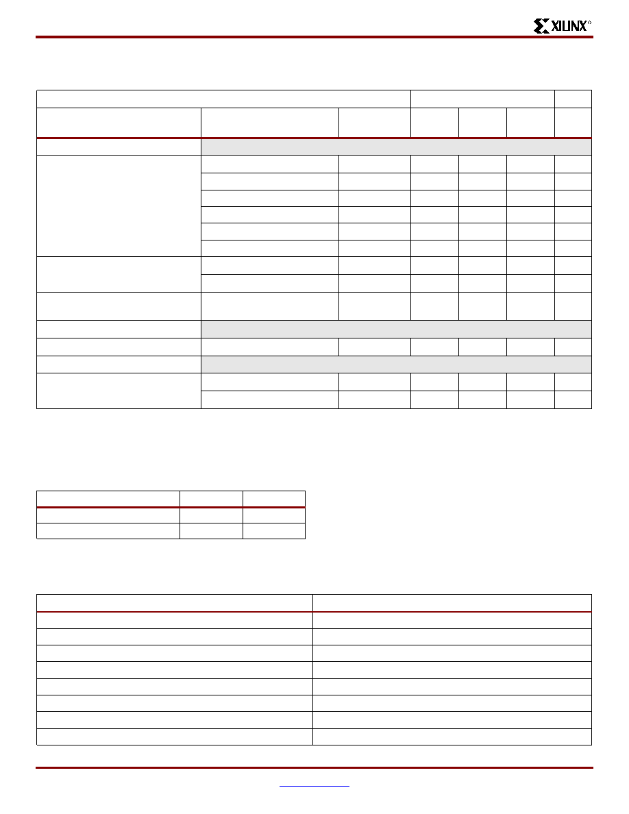
DCM Timing Parameters
R
46
www.xilinx.com
DS083-3 (v2.12) November 11, 2003
1-800-255-7778
Advance Product Specification
Miscellaneous Timing Parameters
Frequency Synthesis
Parameter Cross-Reference
Table 52: Miscellaneous Timing Parameters
Speed Grade
Description
Symbol
Constraints
F
CLKIN
-7
-6
-5
Units
Time Required to Achieve LOCK
Using DLL outputs
(1)
LOCK_DLL:
LOCK_DLL_60
> 60MHz
20.00
20.00
us
LOCK_DLL_50_60
50 - 60 MHz
25.00
25.00
us
LOCK_DLL_40_50
40 - 50 MHz
50.00
50.00
us
LOCK_DLL_30_40
30 - 40 MHz
90.00
90.00
us
LOCK_DLL_24_30
24 - 30 MHz
120.00
120.00
us
Using CLKFX outputs
LOCK_FX_MIN
10.00
10.00
ms
LOCK_FX_MAX
10.00
10.00
ms
Additional lock time with fine phase
shifting
LOCK_DLL_FINE_SHIFT
50.00
50.00
us
Fine Phase Shifting
Absolute shifting range
FINE_SHIFT_RANGE
10.00
10.00
ns
Delay Lines
Tap delay resolution
DCM_TAP_MIN
30.00
30.00
ps
DCM_TAP_MAX
50.00
50.00
ps
Notes:
1.
"DLL outputs" is used here to describe the outputs: CLK0, CLK90, CLK180, CLK270, CLK2X, CLK2X180, and CLKDV.
Table 53: Frequency Synthesis
Attribute
Min
Max
CLKFX_MULTIPLY
2
32
CLKFX_DIVIDE
1
32
Table 54: Parameter Cross-Reference
Libraries Guide
Data Sheet
DLL_CLKOUT_{MIN|MAX}_LF
CLKOUT_FREQ_{1X|2X|DV}_LF
DFS_CLKOUT_{MIN|MAX}_LF
CLKOUT_FREQ_FX_LF
DLL_CLKIN_{MIN|MAX}_LF
CLKIN_FREQ_DLL_LF
DFS_CLKIN_{MIN|MAX}_LF
CLKIN_FREQ_FX_LF
DLL_CLKOUT_{MIN|MAX}_HF
CLKOUT_FREQ_{1X|DV}_HF
DFS_CLKOUT_{MIN|MAX}_HF
CLKOUT_FREQ_FX_HF
DLL_CLKIN_{MIN|MAX}_HF
CLKIN_FREQ_DLL_HF
DFS_CLKIN_{MIN|MAX}_HF
CLKIN_FREQ_FX_HF
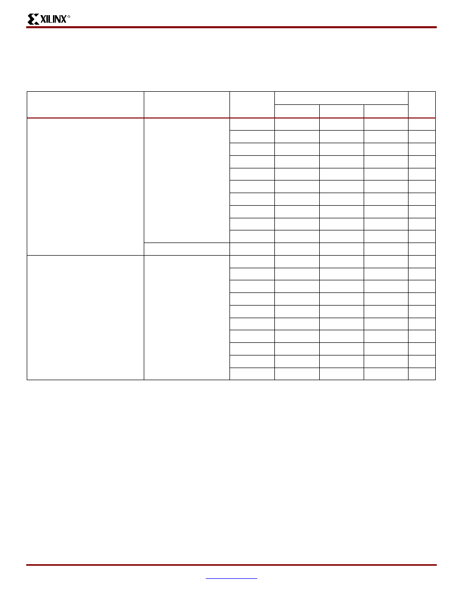
Virtex-II ProTM Platform FPGAs: DC and Switching Characteristics
R
DS083-3 (v2.12) November 11, 2003
www.xilinx.com
47
Advance Product Specification
1-800-255-7778
Source-Synchronous Switching Characteristics
The parameters in this section provide the necessary values for calculating timing budgets for Virtex-II Pro
source-synchronous transmitter and receiver data-valid windows.
Table 55: Duty Cycle Distortion and Clock-Tree Skew
Description
Symbol
Device
Speed Grade
Units
≠
7
≠
6
≠
5
Duty Cycle Distortion
(1)
T
DCD_CLK0
XC2VP2
ns
XC2VP4
ns
XC2VP7
ns
XC2VP20
ns
XC2VP30
ns
XC2VP40
ns
XC2VP50
ns
XC2VP70
ns
XC2VP100
ns
XC2VP125
ns
T
DCD_CLK180
All
ns
Clock Tree Skew
(2)
T
CKSKEW
XC2VP2
ns
XC2VP4
ns
XC2VP7
0.13
0.13
ns
XC2VP20
0.21
0.22
ns
XC2VP30
0.22
0.24
ns
XC2VP40
0.30
0.32
ns
XC2VP50
0.41
0.42
ns
XC2VP70
0.59
0.64
ns
XC2VP100
ns
XC2VP125
ns
Notes:
1.
These parameters represent the worst-case duty cycle distortion observable at the pins of the device using LVDS output buffers. For
cases where other I/O standards are used, IBIS can be used to calculate any additional duty cycle distortion that might be caused by
asymmetrical rise/fall times.
T
DCD_CLK0
applies to cases where local (IOB) inversion is used to provide the negative-edge clock to the DDR element in the I/O.
T
DCD_CLK180
applies to cases where the CLK180 output of the DCM is used to provide the negative-edge clock to the DDR element
in the I/O.
2.
This value represents the worst-case clock-tree skew observable between sequential I/O elements. Significantly less clock-tree skew
exists for I/O registers that are close to each other and fed by the same or adjacent clock-tree branches. Use the Xilinx FPGA_Editor
and Timing Analyzer tools to evaluate clock skew specific to your application.
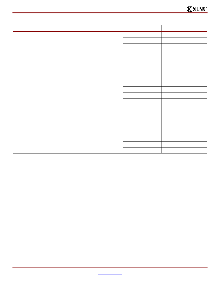
Source-Synchronous Switching Characteristics
R
48
www.xilinx.com
DS083-3 (v2.12) November 11, 2003
1-800-255-7778
Advance Product Specification
Table 56: Package Skew
Description
Symbol
Device/Package
Value
Units
Package Skew
(1)
T
PKGSKEW
XC2VP2FF672
104
ps
XC2VP4FF672
102
ps
XC2VP7FF672
92
ps
XC2VP7FF896
101
ps
XC2VP20FF896
93
ps
XC2VP20FF1152
106
ps
XC2VP30FF896
ps
XC2VP30FF1152
ps
XC2VP40FF1152
92
ps
XC2VP40FF1148
ps
XC2VP40FF1517
104
ps
XC2VP50FF1152
88
ps
XC2VP50FF1148
101
ps
XC2VP50FF1517
97
ps
XC2VP70FF1517
95
ps
XC2VP70FF1704
101
ps
XC2VP100FF1704
ps
XC2VP100FF1696
ps
XC2VP125FF1704
ps
XC2VP125FF1696
ps
Notes:
1.
These values represent the worst-case skew between any two balls of the package: shortest flight time to longest flight time from Pad
to Ball (7.1ps per mm).
2.
Package trace length information is available for these device/package combinations. This information can be used to deskew the
package.

Virtex-II ProTM Platform FPGAs: DC and Switching Characteristics
R
DS083-3 (v2.12) November 11, 2003
www.xilinx.com
49
Advance Product Specification
1-800-255-7778
Table 57: Sample Window
Description
Symbol
Device
Speed Grade
Units
≠
7
≠
6
≠
5
Sampling Error at Receiver Pins
(1)
T
SAMP
XC2VP2
ns
XC2VP4
ns
XC2VP7
0.50
0.50
ns
XC2VP20
0.50
0.50
ns
XC2VP30
0.50
0.50
ns
XC2VP40
0.50
0.50
ns
XC2VP50
0.50
0.50
ns
XC2VP70
0.50
0.50
ns
XC2VP100
ns
XC2VP125
ns
Notes:
1.
This parameter indicates the total sampling error of Virtex-II Pro
DDR input registers across voltage, temperature, and process. The
characterization methodology uses the DCM to capture the DDR input registers' edges of operation. These measurements include:
- CLK0 and CLK180 DCM jitter
- Worst-case Duty-Cycle Distortion - T
DCD_CLK180
- DCM accuracy (phase offset)
- DCM phase shift resolution.
These measurements do not include package or clock tree skew.
Table 58: Pin-to-Pin Setup/Hold: Source-Synchronous Configuration
Description
Symbol
Device
Speed Grade
Units
≠
7
≠
6
≠
5
Data Input Set-Up and Hold Times Relative to a
Forwarded Clock Input Pin, Using DCM and
Global Clock Buffer.
For situations where clock and data inputs
conform to different standards, adjust the setup
and hold values accordingly using the values
shown in IOB Input Switching Characteristics
Standard Adjustments
, page 22
.
No Delay
Global Clock and IFF with DCM
T
PSDCM_0
/T
PHDCM_0
XC2VP2
ns
XC2VP4
ns
XC2VP7
ns
XC2VP20
ns
XC2VP30
ns
XC2VP40
ns
XC2VP50
ns
XC2VP70
ns
XC2VP100
ns
XC2VP125
ns
Notes:
1.
IFF = Input Flip-Flop
2.
The timing values were measured using the fine-phase adjustment feature of the DCM.
3.
The worst-case duty-cycle distortion and DCM jitter on CLK0 and CLK180 is included in these measurements.
Revision History
R
50
www.xilinx.com
DS083-3 (v2.12) November 11, 2003
1-800-255-7778
Advance Product Specification
Source Synchronous Timing Budgets
This section describes how to use the parameters provided
in the
Source-Synchronous Switching Characteristics
sec-
tion to develop system-specific timing budgets. The follow-
ing analysis provides information necessary for determining
Virtex-II Pro contributions to an overall system timing analy-
sis; no assumptions are made about the effects of
Inter-Symbol Interference or PCB skew.
Virtex-II Pro Transmitter Data-Valid Window (T
X
)
T
X
is the minimum aggregate valid data period for a
source-synchronous data bus at the pins of the device and
is calculated as follows:
T
X
= Data Period - [Jitter
(1)
+ Duty Cycle Distortion
(2)
+
TCKSKEW
(3)
+ TPKGSKEW
(4)
]
Notes:
1.
Jitter values and accumulation methodology to be provided in
a future release of this document. The absolute period jitter
values found in the
DCM Timing Parameters
section of the
particular DCM output clock used to clock the IOB FF can be
used for a best case analysis.
2.
This value depends on the clocking methodology used. See
Note1 for
Table 55
.
3.
This value represents the worst-case clock-tree skew
observable between sequential I/O elements. Significantly
less clock-tree skew exists for I/O registers that are close to
each other and fed by the same or adjacent clock-tree
branches. Use the Xilinx FPGA_Editor and Timing Analyzer
tools to evaluate clock skew specific to your application.
4.
These values represent the worst-case skew between any two
balls of the package: shortest flight time to longest flight time
from Pad to Ball.
Virtex-II Pro Receiver Data-Valid Window (R
X
)
R
X
is the required minimum aggregate valid data period for
a source-synchronous data bus at the pins of the device
and is calculated as follows:
R
X
= [TSAMP
(1)
+ TCKSKEW
(2)
+ TPKGSKEW
(3)
]
Notes:
1.
This parameter indicates the total sampling error of
Virtex-II Pro
DDR input registers across voltage, temperature,
and process. The characterization methodology uses the DCM
to capture the DDR input registers' edges of operation. These
measurements include:
-
CLK0 and CLK180 DCM jitter in a quiet system
-
Worst-case duty-cycle distortion
-
DCM accuracy (phase offset)
-
DCM phase shift resolution.
These measurements do not include package or clock tree
skew.
2.
This value represents the worst-case clock-tree skew
observable between sequential I/O elements. Significantly
less clock-tree skew exists for I/O registers that are close to
each other and fed by the same or adjacent clock-tree
branches. Use the Xilinx FPGA_Editor and Timing Analyzer
tools to evaluate clock skew specific to your application.
3.
These values represent the worst-case skew between any two
balls of the package: shortest flight time to longest flight time
from Pad to Ball.
Revision History
This section records the change history for this module of the data sheet.
Date
Version
Revision
01/31/02
1.0
Initial Xilinx release.
06/17/02
2.0
∑
Added new Virtex-II Pro family members.
∑
Added timing parameters from speedsfile v1.62.
∑
Added
Table 37
,
Pipelined Multiplier Switching Characteristics
.
∑
Added 3.3V-vs-2.5V table entries for some parameters.
09/03/02
2.1
∑
Added
Source-Synchronous Switching Characteristics
section.
∑
Added absolute max ratings for 3.3V-vs-2.5V parameters in
Table 1
.
∑
Added recommended operating conditions for V
IN
and RocketIO footnote to
Table 2
.
∑
Updated SSTL2 values in
Table 6
. Added SSTL18 values:
Table 6
,
Table 31
,
Table 32
.
[
Table 32
removed in v2.8.]
∑
Added
Table 10
, which contains LVPECL DC specifications.
09/27/02
2.2
Added section
General Power Supply Requirements
.
Virtex-II ProTM Platform FPGAs: DC and Switching Characteristics
R
DS083-3 (v2.12) November 11, 2003
www.xilinx.com
51
Advance Product Specification
1-800-255-7778
11/20/02
2.3
Updated parametric information in:
∑
Table 1
: Increase Absolute Max Rating for V
CCO
, V
REF
, V
IN
, and V
TS
from 3.6V to
3.75V. Delete cautionary footnotes related to voltage overshoot/undershoot.
∑
Table 2
: Delete V
CCO
specifications for 2.5V and below operation. Delete footnote
referencing special information for 3.3V operation. Add footnote for PCI/PCI-X.
∑
Table 3
: Add I
BATT
. Delete I
L
specifications for 2.5V and below operation.
∑
Table 4
: Add Typical Quiescent Supply Currents for XC2VP4 and XC2VP7 only
∑
Table 6
: Correct I
OL
and I
OH
for SSTL2 I. Add rows for LVTTL, LVCMOS33, and PCI-X.
Correct max V
IH
from V
CCO
to 3.6V.
∑
Table 7
: Correct Min/Max V
OD
, V
OCM
, and V
ICM
∑
Table 10
: Reformat LVPECL DC Specifications to match Virtex-II data sheet format
∑
Table 11
: Correct parameter name from Differential Output Voltage to Single-Ended
Output Voltage Swing.
∑
Table 15
: Add CPMC405CLOCK max frequencies
∑
Table 23
: Add footnote regarding serial data rate limitation in -5 part.
∑
Table 31
: Add rows for LVTTL, LVCMOS33, and PCI-X.
∑
Table 32
: Add LVTTL, LVCMOS33, and PCI-X. Correct all capacitive load values
(except PCI/PCI-X) to 0 pF. [
Table 32
removed in v2.8.]
∑
Table 42
: Correct CCLK max frequencies
11/25/02
2.4
Table 1
: Correct lower limit of voltage range of V
IN
and V
TS
from ≠0.3V to ≠0.5V for 3.3V.
12/03/02
2.5
Updated parametric information in:
∑
Table 1
: Correct lower limit of voltage range of V
IN
and V
TS
from ≠0.5V to ≠0.3V for
3.3V.
∑
Table 2
: Add footnote (2) regarding V
CCAUX
voltage droop. Renumbered other notes.
∑
Table 11
: Add waveform diagrams (
Figure 1
and
Figure 2
) illustrating DV
OUT
(single-ended) and DV
PPOUT
(differential).
∑
Table 21
: Indicate REFCLK upper frequency limitation; relate REFCLK parameters to
REFCLK2, BREFCLK, and BREFCLK2; correct T
RCLK
and T
FCLK
values and unit of
measurement.
∑
Table 51
: Add qualifying footnote to CLKOUT_DUTY_CYCLE_DLL
.
01/20/03
2.6
Updated parametric information in:
∑
Table 11
: Correct DV
IN
Min (200 mV to 175 mV) and DV
IN
Max (1000 mV to 2000 mV).
∑
Table 21
: Correct T
RCLK
/T
FCLK
Typ (400 ps to 600 ps) and Max (600 ps to 1000 ps).
Add footnote (2) to qualify Max T
GJTT
parameter.
∑
Table 50
: Correct hyperlink in footnote (1) to point directly to Answer Record 13645.
∑
Move clock parameters from
Table 17
,
Table 18
,
Table 19
, and
Table 20
to
Table 15
.
03/24/03
2.7
∑
Added/updated timing parameters from speedsfile v1.76.
∑
Table 2
: Delete first table footnote and renumber all others.
∑
Table 3
: Add "sample-tested" to I
L
. Remove "Device" column, unnecessary.
∑
Table 8
: Update V
OCM
(Typ) to 1.250V.
∑
Table 10
: Update LVPECL_25 DC parameters.
∑
Table 21
: Update F
GCLK
frequency ranges. Break out T
GJTT
by operating speed.
∑
Table 23
: Update F
GTX
frequency ranges. Correct T
DJ
to 0.17 UI, T
RJ
to o.18 UI.
∑
Table 31
: Update V
REF
(Typ) for HSTL Class I/II from 1.08V to 0.90V.
∑
Table 34
,
Table 35
: Correct parameter name "CE input (WS)" to "SR input".
∑
Table 55
: Break out T
DCD_CLK0
by device type.
Date
Version
Revision

Revision History
R
52
www.xilinx.com
DS083-3 (v2.12) November 11, 2003
1-800-255-7778
Advance Product Specification
05/27/03
2.8
∑
Updated time and frequency parameters as per speedsfile v1.78.
∑
Table 3
: Added values for I
REF
, I
L
, I
RPU
, I
RPD
∑
Corrected I
CCINTQ
(
Table 4
) and I
CCINTMIN
(
Table 5
) for XC2VP20 to 600 mA.
∑
Table 4
: Updated/Added Typ and Max quiescent current values for XC2VP7 and
XC2VP20. Added footnote specifying parameters are for Commercial Grade parts.
∑
Table 5
: Added footnote specifying parameters are for Commercial Grade parts.
∑
Table 6
: Corrected V
IH
(Max) for LVTTL and LVCMOS33 standards from 3.6V to 3.45V.
Changed V
IL
(Min) for all standards to ≠0.2V. Corrected V
IL
(Max) for LVCMOS15 and
LVCMOS18 from 20% V
CCO
to 30% V
CCO
.
∑
Table 10
: Corrected LVPECL_25 Min and Max values for V
IH
and V
IL
. Added
explanatory text above table.
∑
Table 12
and
Table 13
(pin-pin and reg-reg performance): Changed device specified
from XC2VP7FF672-6 to XC2VP20FF1152-6.
∑
Table 14
: Updated to show devices XC2VP7 and XC2VP20 as Preliminary for the -6
speed grade and Production for the -5 speed grade.
∑
Removed former Table 32, Standard Capacitive Loads.
∑
Table 43
: Updated T
TAPTCK
from 4.0 ns to 5.5 ns.
∑
Table 50
: Modified footnote referenced at CLKFX/CLKFX180 to point to the online
Jitter Calculator.
∑
Added
Figure 6
and accompanying procedure for measuring standard adjustments.
∑
Table 1
: Footnote (2) rewritten to specify "one or more banks."
∑
Table 48
: Some DCM parameters were erroneously missing from v2.8 (single-module
version) due to a document compilation error. The concatenated full data sheet version
was not affected. These parameters have been restored.
08/25/03
2.9
∑
Updated time and frequency parameters as per speedsfile v1.81.
∑
Table 1
: Footnote (2) rewritten to specify "one or more banks."
∑
Table 2
: Added footnote referring to XAPP659 for 3.3V I/O operation.
∑
Table 44
and
Table 45
: Revised test setup footnote to refer to
Figure 6
. Previously
specified a capacitive load parameter.
∑
Table 48
: Due to a document compilation error in v2.8, some DCM parameters were
erroneously omitted from the full data sheet file (all four modules concatenated),
though not from the stand-alone Module 3 file. The omitted parameters have been
restored.
∑
Table 55
and
Table 57
: Corrected parameters to expression in picoseconds, as
labeled. Previously expressed in nanoseconds, but labeled picoseconds.
∑
Figure 6: Added note to figure regarding termination resistors.
∑
Table 5
: Added I
CCINTMIN
for XC2VP30 device.
09/10/03
2.10
∑
Figure 7
: Changed representation of mode pins M0, M1, and M2 indicating that they
must be held to a constant DC level during and after configuration.
∑
Table 40
: Added footnote indicating that mode pins M0, M1, and M2 must be held to a
constant DC level during and after configuration.
Date
Version
Revision

Virtex-II ProTM Platform FPGAs: DC and Switching Characteristics
R
DS083-3 (v2.12) November 11, 2003
www.xilinx.com
53
Advance Product Specification
1-800-255-7778
Virtex-II Pro Data Sheet
The Virtex-II Pro Data Sheet contains the following modules:
∑
Virtex-II ProTM Platform FPGAs: Introduction and
Overview (Module 1)
∑
Virtex-II ProTM Platform FPGAs: Functional Description
(Module 2)
∑
Virtex-II ProTM Platform FPGAs: DC and Switching
Characteristics (Module 3)
∑
Virtex-II ProTM Platform FPGAs: Pinout Information
(Module 4)
10/14/03
2.11
∑
Table 1
: Deleted Footnote (2), which had derated the absolute maximum T
J
when one
or more banks operated at 3.3V. Changed T
J
description from "Operating junction
temperature" to "Maximum junction temperature". Added new Footnote (2) linking to
website for package thermal data.
∑
Table 4
and
Table 5
: Filled in power-on and quiescent current parameters for all
devices through XC2VP70. Added Industrial Grade multiplier specification to Footnote
(1) in both tables.
∑
In section
General Power Supply Requirements
, replaced reference to Answer Record
11713 with reference to
XAPP689
regarding handling of simultaneously switching
outputs (SSO).
∑
In section
I/O Standard Adjustment Measurement Methodology
:
-
Table 31
renamed
Input Delay Measurement Methodology
. Added footnotes.
-
Added new
Table 32
,
Output Delay Measurement Methodology
.
-
Replaced
Figure 6
,
Generalized Test Setup
, with new drawing.
-
Revised and extended text describing output delay measurement procedure.
∑
Table 49
: For Input Clock Low/High Pulse Width, PSCLK and CLKIN, changed existing
Footnote (2) to new Footnote (3).
11/10/03
2.12
∑
Table 1
: Changed 3.3V absolute max V
IN
and V
TS
from 3.75V to 4.05V. Added
footnote referring to
XAPP659
.
∑
Table 4
: Removed MIN column from table.
Date
Version
Revision

Virtex-II Pro Data Sheet
R
54
www.xilinx.com
DS083-3 (v2.12) November 11, 2003
1-800-255-7778
Advance Product Specification
© 2003 Xilinx, Inc. All rights reserved. All Xilinx trademarks, registered trademarks, patents, and disclaimers are as listed at
http://www.xilinx.com/legal.htm
.
All other trademarks and registered trademarks are the property of their respective owners. All specifications are subject to change without notice.
DS083-4 (v2.5.5) August 25, 2003
www.xilinx.com
1
Advance Product Specification
1-800-255-7778
This document provides
Virtex-II Pro Device/Package Com-
binations and Maximum I/Os
and
Virtex-II Pro Pin Defini-
tions
, followed by pinout tables, for these packages:
∑
FG256 Fine-Pitch BGA Package
∑
FG456 Fine-Pitch BGA Package
∑
FG676 Fine-Pitch BGA Package
∑
FF672 Flip-Chip Fine-Pitch BGA Package
∑
FF896 Flip-Chip Fine-Pitch BGA Package
∑
FF1152 Flip-Chip Fine-Pitch BGA Package
∑
FF1148 Flip-Chip Fine-Pitch BGA Package
∑
FF1517 Flip-Chip Fine-Pitch BGA Package
∑
FF1704 Flip-Chip Fine-Pitch BGA Package
∑
FF1696 Flip-Chip Fine-Pitch BGA Package
For device pinout diagrams and layout guidelines, refer to
the
Virtex-II Pro Platform FPGA User Guide
. ASCII pack-
age pinout files are also available for download from the Xil-
inx website (
www.xilinx.com
).
Virtex-II Pro Device/Package Combinations and Maximum I/Os
Wire-bond and flip-chip packages are available.
Table 1
and
Table 2
show the maximum number of user I/Os possible in
wire-bond and flip-chip packages, respectively.
∑
FG denotes wire-bond fine-pitch BGA (1.00 mm pitch).
∑
FF denotes flip-chip fine-pitch BGA (1.00 mm pitch)
.
Table 3
shows the number of available I/Os, the number of RocketIOTM multi-gigabit transceiver (MGT) pins, and the number
of differential I/O pairs for each Virtex-II Pro device/package combination. The number of I/Os per package includes all user
I/Os except the fifteen control pins (CCLK, DONE, M0, M1, M2, PROG_B, PWRDWN_B, TCK, TDI, TDO, TMS,
HSWAP_EN, DXN, DXP, AND RSVD) and the nine (per transceiver) RocketIO MGT pins (TXP, TXN, RXP, RXN,
AVCCAUXTX, AVCCAUXRX, VTTX, VTRX, and GNDA). The number of transceivers in the device is the number of
RocketIO MGT pins in
Table 3
divided by nine.
0
298
Virtex-II ProTM Platform FPGAs:
Pinout Information
DS083-4 (v2.5.5) August 25, 2003
0
0
Advance Product Specification
R
Table 1: Wire-Bond Packages Information
Package
FG256
FG456
FG676
Pitch (mm)
1.00
1.00
1.00
Size (mm)
17 x 17
23 x 23
26 x 26
Maximum I/Os
140
248
412
Table 2: Flip-Chip Packages Information
Package
FF672
FF896
FF1152
FF1148
FF1517
FF1704
FF1696
Pitch (mm)
1.00
1.00
1.00
1.00
1.00
1.00
1.00
Size (mm)
27 x 27
31 x 31
35 x 35
35 x 35
40 x 40
42.5 x 42.5
42.5 x 42.5
Maximum I/Os
396
556
644
812
964
1040
1200
Table 3: Virtex-II Pro Available I/Os and RocketIO MGT Pins per Device/Package Combination
Virtex-II Pro
Device
User I/Os &
RocketIO
MGT Pins
Virtex-II Pro Package
FG256
FG456
FG676
FF672
FF896
FF1152
FF1148
FF1517
FF1704
FF1696
XC2VP2
Available
User I/Os
140
156
-
204
-
-
-
-
-
-
RocketIO
MGT Pins
36
36
-
36
-
-
-
-
-
-
Differential
I/O Pairs
68
76
-
100
-
-
-
-
-
-

Virtex-II Pro Device/Package Combinations and Maximum I/Os
R
2
www.xilinx.com
DS083-4 (v2.5.5) August 25, 2003
1-800-255-7778
Advance Product Specification
XC2VP4
Available
User I/Os
140
248
-
348
-
-
-
-
-
-
RocketIO
MGT Pins
36
36
-
36
-
-
-
-
-
-
Differential
I/O Pairs
68
122
-
172
-
-
-
-
-
-
XC2VP7
Available
User I/Os
-
248
-
396
396
-
-
-
-
-
RocketIO
MGT Pins
-
72
-
72
72
-
-
-
-
-
Differential
I/O Pairs
-
122
-
196
196
-
-
-
-
-
XC2VP20
Available
User I/Os
-
-
404
-
556
564
-
-
-
-
RocketIO
MGT Pins
-
-
72
-
72
72
-
-
-
-
Differential
I/O Pairs
-
-
196
-
272
276
-
-
-
-
XC2VP30
Available
User I/Os
-
-
416
-
556
644
-
-
-
-
RocketIO
MGT Pins
-
-
72
-
72
72
-
-
-
-
Differential
I/O Pairs
-
-
202
-
272
340
-
-
-
-
XC2VP40
Available
User I/Os
-
-
416
-
-
692
804
-
-
-
RocketIO
MGT Pins
-
-
72
-
-
108
0
-
-
-
Differential
I/O Pairs
-
-
202
-
-
340
396
-
-
-
XC2VP50
Available
User I/Os
-
-
-
-
692
812
852
-
-
RocketIO
MGT Pins
-
-
-
-
144
0
144
-
-
Differential
I/O Pairs
-
-
-
-
340
400
420
-
-
XC2VP70
Available
User I/Os
-
-
-
-
-
-
964
996
-
RocketIO
MGT Pins
-
-
-
-
-
-
144
180
-
Differential
I/O Pairs
-
-
-
-
-
-
476
492
-
Table 3: Virtex-II Pro Available I/Os and RocketIO MGT Pins per Device/Package Combination (Continued)
Virtex-II Pro
Device
User I/Os &
RocketIO
MGT Pins
Virtex-II Pro Package
FG256
FG456
FG676
FF672
FF896
FF1152
FF1148
FF1517
FF1704
FF1696
Virtex-II ProTM Platform FPGAs: Pinout Information
R
DS083-4 (v2.5.5) August 25, 2003
www.xilinx.com
3
Advance Product Specification
1-800-255-7778
Virtex-II Pro
Pin Definitions
This section describes the pinouts for Virtex-II Pro devices
in the following packages:
∑
FG256, FG456, and FG676: wire-bond fine-pitch BGA
of 1.00 mm pitch
∑
FF672, FF896, FF1148, FF1152, FF1517, FF1696,
and FF1704: flip-chip fine-pitch BGA of 1.00 mm pitch
All of the devices supported in a particular package are
pinout-compatible and are listed in the same table (one
table per package). Pins that are not available for smaller
devices are listed in right-hand columns.
Each device is split into eight I/O banks to allow for flexibility
in the choice of I/O standards. Global pins, including JTAG,
configuration, and power/ground pins, are listed at the end
of each table.
Table 4
provides definitions for all pin types.
All Virtex-II Pro pinout tables are available on the distribu-
tion CD-ROM, or on the web (at
http://www.xilinx.com
).
Pin Definitions
Table 4
provides a description of each pin type listed in Virtex-II Pro pinout tables.
XC2VP100
Available
User I/Os
-
-
-
-
-
-
-
1040
1164
RocketIO
MGT Pins
-
-
-
-
-
-
-
180
0
Differential
I/O Pairs
-
-
-
-
-
-
-
512
572
XC2VP125
Available
User I/Os
-
-
-
-
-
-
-
1040
1200
RocketIO
MGT Pins
-
-
-
-
-
-
-
180
0
Differential
I/O Pairs
-
-
-
-
-
-
-
512
590
Table 3: Virtex-II Pro Available I/Os and RocketIO MGT Pins per Device/Package Combination (Continued)
Virtex-II Pro
Device
User I/Os &
RocketIO
MGT Pins
Virtex-II Pro Package
FG256
FG456
FG676
FF672
FF896
FF1152
FF1148
FF1517
FF1704
FF1696
Table 4: Virtex-II Pro Pin Definitions
Pin Name
Direction
Description
User I/O Pins
IO_LXXY_#
Input/Output
All user I/O pins are capable of differential signalling and can implement LVDS, ULVDS,
BLVDS, LVPECL, or LDT pairs. Each user I/O is labeled "IO_LXXY_#", where:
IO indicates a user I/O pin.
LXXY indicates a differential pair, with XX a unique pair in the bank and Y = P/N for
the positive and negative sides of the differential pair.
# indicates the bank number (0 through 7)
Dual-Function Pins
IO_LXXY_#/ZZZ
The dual-function pins are labelled "IO_LXXY_#/ZZZ", where ZZZ can be one of the
following pins:
Per Bank - VRP, VRN, or VREF
Globally - GCLKX(S/P), BUSY/DOUT, INIT_B, D0/DIN ≠ D7, RDWR_B, or CS_B
Virtex-II Pro Pin Definitions
R
4
www.xilinx.com
DS083-4 (v2.5.5) August 25, 2003
1-800-255-7778
Advance Product Specification
With /ZZZ:
D0/DIN, D1, D2,
D3, D4, D5, D6,
D7
Input/Output ∑
In SelectMAP mode, D0 through D7 are configuration data pins. These pins
become user I/Os after configuration, unless the SelectMAP port is retained.
∑
In bit-serial modes, DIN (D0) is the single-data input. This pin becomes a user I/O
after configuration.
CS_B
Input
In SelectMAP mode, this is the active-low Chip Select signal. The pin becomes a user
I/O after configuration, unless the SelectMAP port is retained.
RDWR_B
Input
In SelectMAP mode, this is the active-low Write Enable signal. The pin becomes a user
I/O after configuration, unless the SelectMAP port is retained.
BUSY/DOUT
Output
∑
In SelectMAP mode, BUSY controls the rate at which configuration data is loaded.
The pin becomes a user I/O after configuration, unless the SelectMAP port is
retained.
∑
In bit-serial modes, DOUT provides preamble and configuration data to
downstream devices in a daisy-chain. The pin becomes a user I/O after
configuration.
INIT_B
Bidirectional
(open-drain)
When Low, this pin indicates that the configuration memory is being cleared. When held
Low, the start of configuration is delayed. During configuration, a Low on this output
indicates that a configuration data error has occurred. The pin becomes a user I/O after
configuration.
GCLKx (S/P)
Input/Output
These are clock input pins that connect to Global Clock Buffers. These pins become
regular user I/Os when not needed for clocks.
VRP
Input
This pin is for the DCI voltage reference resistor of P transistor (per bank).
VRN
Input
This pin is for the DCI voltage reference resistor of N transistor (per bank).
V
REF
Input
These are input threshold voltage pins. They become user I/Os when an external
threshold voltage is not needed (per bank).
Dedicated Pins
(1)
CCLK
Input/Output
Configuration clock. Output in Master mode or Input in Slave mode.
PROG_B
Input
Active Low asynchronous reset to configuration logic. This pin has a permanent weak
pull-up resistor.
DONE
Input/Output
DONE is a bidirectional signal with an optional internal pull-up resistor. As an output,
this pin indicates completion of the configuration process. As an input, a Low level on
DONE can be configured to delay the start-up sequence.
M2, M1, M0
Input
Configuration mode selection.
HSWAP_EN
Input
Enable I/O pullups during configuration.
TCK
Input
Boundary Scan Clock.
TDI
Input
Boundary Scan Data Input.
TDO
Output
(open-drain)
Boundary Scan Data Output.
TMS
Input
Boundary Scan Mode Select.
PWRDWN_B
Input
(unsupported)
Active Low power-down pin (unsupported). Driving this pin Low can adversely affect
device operation and configuration. PWRDWN_B is internally pulled High, which is its
default state. It does not require an external pull-up.
Table 4: Virtex-II Pro Pin Definitions (Continued)
Pin Name
Direction
Description
Virtex-II ProTM Platform FPGAs: Pinout Information
R
DS083-4 (v2.5.5) August 25, 2003
www.xilinx.com
5
Advance Product Specification
1-800-255-7778
BREFCLK Pin Definitions
These dedicated clocks use the same clock inputs for all packages:
Other Pins
DXN, DXP
N/A
Temperature-sensing diode pins (Anode: DXP, Cathode: DXN).
V
BATT
Input
Decryptor key memory backup supply. (Do not connect if battery is not used.)
RSVD
N/A
Reserved pin - do not connect.
V
CCO
Input
Power-supply pins for the output drivers (per bank).
V
CCAUX
Input
Power-supply pins for auxiliary circuits.
V
CCINT
Input
Power-supply pins for the internal core logic.
GND
Input
Ground.
AVCCAUXRX#
Input
Analog power supply for receive circuitry of the RocketIO multi-gigabit transceiver
(2.5V).
AVCCAUXTX#
Input
Analog power supply for transmit circuitry of the RocketIO multi-gigabit transceiver
(2.5V).
VTRXPAD#
Input
Receive termination supply for the RocketIO multi-gigabit transceiver (1.8V - 2.8V).
VTTXPAD#
Input
Transmit termination supply for the RocketIO multi-gigabit transceiver (1.8V - 2.8V).
GNDA#
(2)
Input
Ground for the analog circuitry of the RocketIO multi-gigabit transceiver.
RXPPAD#
Input
Positive differential receive port of the RocketIO multi-gigabit transceiver.
RXNPAD#
Input
Negative differential receive port of the RocketIO multi-gigabit transceiver.
TXPPAD#
Output
Positive differential transmit port of the RocketIO multi-gigabit transceiver.
TXNPAD#
Output
Negative differential transmit port of the RocketIO multi-gigabit transceiver.
Notes:
1.
All dedicated pins (JTAG and configuration) are powered by V
CCAUX
(independent of the bank V
CCO
voltage).
Top
BREFCLK
P
GCLK4S
Bottom
BREFCLK
P
GCLK6P
N
GCLK5P
N
GCLK7S
BREFCLK2
P
GCLK2S
BREFCLK2
P
GCLK0P
N
GCLK3P
N
GCLK1S
Table 4: Virtex-II Pro Pin Definitions (Continued)
Pin Name
Direction
Description
FG256 Fine-Pitch BGA Package
R
6
www.xilinx.com
DS083-4 (v2.5.5) August 25, 2003
1-800-255-7778
Advance Product Specification
FG256 Fine-Pitch BGA Package
As shown in
Table 5
, XC2VP2 and XC2VP4 Virtex-II Pro devices are available in the FG256 fine-pitch BGA package. The
pins in each of these devices are identical. Following this table are the
FG256 Fine-Pitch BGA Package Specifications
(1.00mm pitch)
.
Table 5: FG256 -- XC2VP2 and XC2VP4
Bank
Pin Description
Pin Number
0
IO_L01N_0/VRP_0
C2
0
IO_L01P_0/VRN_0
C3
0
IO_L02N_0
B3
0
IO_L02P_0
C4
0
IO_L03N_0
A2
0
IO_L03P_0/VREF_0
A3
0
IO_L06N_0
D5
0
IO_L06P_0
C5
0
IO_L07P_0
D6
0
IO_L09N_0
E6
0
IO_L09P_0/VREF_0
E7
0
IO_L69N_0
D7
0
IO_L69P_0/VREF_0
C7
0
IO_L74N_0/GCLK7P
D8
0
IO_L74P_0/GCLK6S
C8
0
IO_L75N_0/GCLK5P
B8
0
IO_L75P_0/GCLK4S
A8
1
IO_L75N_1/GCLK3P
A9
1
IO_L75P_1/GCLK2S
B9
1
IO_L74N_1/GCLK1P
C9
1
IO_L74P_1/GCLK0S
D9
1
IO_L69N_1/VREF_1
C10
1
IO_L69P_1
D10
1
IO_L09N_1/VREF_1
E10
1
IO_L09P_1
E11
1
IO_L07N_1
D11
1
IO_L06N_1
C12
1
IO_L06P_1
D12
1
IO_L03N_1/VREF_1
A14
1
IO_L03P_1
A15
Virtex-II ProTM Platform FPGAs: Pinout Information
R
DS083-4 (v2.5.5) August 25, 2003
www.xilinx.com
7
Advance Product Specification
1-800-255-7778
1
IO_L02N_1
C13
1
IO_L02P_1
B14
1
IO_L01N_1/VRP_1
C14
1
IO_L01P_1/VRN_1
C15
2
IO_L01N_2/VRP_2
E14
2
IO_L01P_2/VRN_2
E15
2
IO_L02N_2
E13
2
IO_L02P_2
F12
2
IO_L03N_2
F13
2
IO_L03P_2
F14
2
IO_L04N_2/VREF_2
F15
2
IO_L04P_2
F16
2
IO_L06N_2
G13
2
IO_L06P_2
G14
2
IO_L85N_2
G15
2
IO_L85P_2
G16
2
IO_L86N_2
G12
2
IO_L86P_2
H13
2
IO_L88N_2/VREF_2
H14
2
IO_L88P_2
H15
2
IO_L90N_2
H16
2
IO_L90P_2
J16
3
IO_L90N_3
J15
3
IO_L90P_3
J14
3
IO_L89N_3
J13
3
IO_L89P_3
K12
3
IO_L87N_3/VREF_3
K16
3
IO_L87P_3
K15
3
IO_L85N_3
K14
3
IO_L85P_3
K13
3
IO_L06N_3
L16
3
IO_L06P_3
L15
3
IO_L05N_3
L14
Table 5: FG256 -- XC2VP2 and XC2VP4
Bank
Pin Description
Pin Number
FG256 Fine-Pitch BGA Package
R
8
www.xilinx.com
DS083-4 (v2.5.5) August 25, 2003
1-800-255-7778
Advance Product Specification
3
IO_L05P_3
L13
3
IO_L03N_3/VREF_3
L12
3
IO_L03P_3
M13
3
IO_L02N_3
M16
3
IO_L02P_3
N16
3
IO_L01N_3/VRP_3
M15
3
IO_L01P_3/VRN_3
M14
4
IO_L01N_4/BUSY/DOUT
(1)
P15
4
IO_L01P_4/INIT_B
P14
4
IO_L02N_4/D0/DIN
(1)
R14
4
IO_L02P_4/D1
P13
4
IO_L03N_4/D2
T15
4
IO_L03P_4/D3
T14
4
IO_L06N_4/VRP_4
N12
4
IO_L06P_4/VRN_4
P12
4
IO_L07P_4/VREF_4
N11
4
IO_L09N_4
M11
4
IO_L09P_4/VREF_4
M10
4
IO_L69N_4
N10
4
IO_L69P_4/VREF_4
P10
4
IO_L74N_4/GCLK3S
N9
4
IO_L74P_4/GCLK2P
P9
4
IO_L75N_4/GCLK1S
R9
4
IO_L75P_4/GCLK0P
T9
5
IO_L75N_5/GCLK7S
T8
5
IO_L75P_5/GCLK6P
R8
5
IO_L74N_5/GCLK5S
P8
5
IO_L74P_5/GCLK4P
N8
5
IO_L69N_5/VREF_5
P7
5
IO_L69P_5
N7
5
IO_L09N_5/VREF_5
M7
5
IO_L09P_5
M6
5
IO_L07N_5/VREF_5
N6
Table 5: FG256 -- XC2VP2 and XC2VP4
Bank
Pin Description
Pin Number
Virtex-II ProTM Platform FPGAs: Pinout Information
R
DS083-4 (v2.5.5) August 25, 2003
www.xilinx.com
9
Advance Product Specification
1-800-255-7778
5
IO_L06N_5/VRP_5
P5
5
IO_L06P_5/VRN_5
N5
5
IO_L03N_5/D4
T3
5
IO_L03P_5/D5
T2
5
IO_L02N_5/D6
P4
5
IO_L02P_5/D7
R3
5
IO_L01N_5/RDWR_B
P3
5
IO_L01P_5/CS_B
P2
6
IO_L01P_6/VRN_6
M3
6
IO_L01N_6/VRP_6
M2
6
IO_L02P_6
N1
6
IO_L02N_6
M1
6
IO_L03P_6
M4
6
IO_L03N_6/VREF_6
L5
6
IO_L05P_6
L4
6
IO_L05N_6
L3
6
IO_L06P_6
L2
6
IO_L06N_6
L1
6
IO_L85P_6
K4
6
IO_L85N_6
K3
6
IO_L87P_6
K2
6
IO_L87N_6/VREF_6
K1
6
IO_L89P_6
K5
6
IO_L89N_6
J4
6
IO_L90P_6
J3
6
IO_L90N_6
J2
7
IO_L90P_7
J1
7
IO_L90N_7
H1
7
IO_L88P_7
H2
7
IO_L88N_7/VREF_7
H3
7
IO_L86P_7
H4
7
IO_L86N_7
G5
7
IO_L85P_7
G1
Table 5: FG256 -- XC2VP2 and XC2VP4
Bank
Pin Description
Pin Number
FG256 Fine-Pitch BGA Package
R
10
www.xilinx.com
DS083-4 (v2.5.5) August 25, 2003
1-800-255-7778
Advance Product Specification
7
IO_L85N_7
G2
7
IO_L06P_7
G3
7
IO_L06N_7
G4
7
IO_L04P_7
F1
7
IO_L04N_7/VREF_7
F2
7
IO_L03P_7
F3
7
IO_L03N_7
F4
7
IO_L02P_7
F5
7
IO_L02N_7
E4
7
IO_L01P_7/VRN_7
E2
7
IO_L01N_7/VRP_7
E3
0
VCCO_0
F8
0
VCCO_0
F7
0
VCCO_0
E8
1
VCCO_1
F9
1
VCCO_1
F10
1
VCCO_1
E9
2
VCCO_2
H12
2
VCCO_2
H11
2
VCCO_2
G11
3
VCCO_3
K11
3
VCCO_3
J12
3
VCCO_3
J11
4
VCCO_4
M9
4
VCCO_4
L9
4
VCCO_4
L10
5
VCCO_5
M8
5
VCCO_5
L8
5
VCCO_5
L7
6
VCCO_6
K6
6
VCCO_6
J6
6
VCCO_6
J5
7
VCCO_7
H6
7
VCCO_7
H5
Table 5: FG256 -- XC2VP2 and XC2VP4
Bank
Pin Description
Pin Number
Virtex-II ProTM Platform FPGAs: Pinout Information
R
DS083-4 (v2.5.5) August 25, 2003
www.xilinx.com
11
Advance Product Specification
1-800-255-7778
7
VCCO_7
G6
N/A
CCLK
N15
N/A
PROG_B
D1
N/A
DONE
P16
N/A
M0
N3
N/A
M1
N2
N/A
M2
P1
N/A
TCK
D16
N/A
TDI
E1
N/A
TDO
E16
N/A
TMS
C16
N/A
PWRDWN_B
N14
N/A
HSWAP_EN
C1
N/A
RSVD
D14
N/A
VBATT
D15
N/A
DXP
D2
N/A
DXN
D3
N/A
AVCCAUXTX6
B5
N/A
VTTXPAD6
B4
N/A
TXNPAD6
A4
N/A
TXPPAD6
A5
N/A
GNDA6
C6
N/A
RXPPAD6
A6
N/A
RXNPAD6
A7
N/A
VTRXPAD6
B6
N/A
AVCCAUXRX6
B7
N/A
AVCCAUXTX7
B11
N/A
VTTXPAD7
B10
N/A
TXNPAD7
A10
N/A
TXPPAD7
A11
N/A
GNDA7
C11
N/A
RXPPAD7
A12
N/A
RXNPAD7
A13
N/A
VTRXPAD7
B12
Table 5: FG256 -- XC2VP2 and XC2VP4
Bank
Pin Description
Pin Number
FG256 Fine-Pitch BGA Package
R
12
www.xilinx.com
DS083-4 (v2.5.5) August 25, 2003
1-800-255-7778
Advance Product Specification
N/A
AVCCAUXRX7
B13
N/A
AVCCAUXRX18
R13
N/A
VTRXPAD18
R12
N/A
RXNPAD18
T13
N/A
RXPPAD18
T12
N/A
GNDA18
P11
N/A
TXPPAD18
T11
N/A
TXNPAD18
T10
N/A
VTTXPAD18
R10
N/A
AVCCAUXTX18
R11
N/A
AVCCAUXRX19
R7
N/A
VTRXPAD19
R6
N/A
RXNPAD19
T7
N/A
RXPPAD19
T6
N/A
GNDA19
P6
N/A
TXPPAD19
T5
N/A
TXNPAD19
T4
N/A
VTTXPAD19
R4
N/A
AVCCAUXTX19
R5
N/A
VCCINT
N4
N/A
VCCINT
N13
N/A
VCCINT
M5
N/A
VCCINT
M12
N/A
VCCINT
E5
N/A
VCCINT
E12
N/A
VCCINT
D4
N/A
VCCINT
D13
N/A
VCCAUX
R16
N/A
VCCAUX
R1
N/A
VCCAUX
B16
N/A
VCCAUX
B1
N/A
GND
T16
N/A
GND
T1
N/A
GND
R2
Table 5: FG256 -- XC2VP2 and XC2VP4
Bank
Pin Description
Pin Number
Virtex-II ProTM Platform FPGAs: Pinout Information
R
DS083-4 (v2.5.5) August 25, 2003
www.xilinx.com
13
Advance Product Specification
1-800-255-7778
N/A
GND
R15
N/A
GND
L6
N/A
GND
L11
N/A
GND
K9
N/A
GND
K8
N/A
GND
K7
N/A
GND
K10
N/A
GND
J9
N/A
GND
J8
N/A
GND
J7
N/A
GND
J10
N/A
GND
H9
N/A
GND
H8
N/A
GND
H7
N/A
GND
H10
N/A
GND
G9
N/A
GND
G8
N/A
GND
G7
N/A
GND
G10
N/A
GND
F6
N/A
GND
F11
N/A
GND
B2
N/A
GND
B15
N/A
GND
A16
N/A
GND
A1
Notes:
1.
See
Table 4
for an explanation of the signals available on this pin.
Table 5: FG256 -- XC2VP2 and XC2VP4
Bank
Pin Description
Pin Number
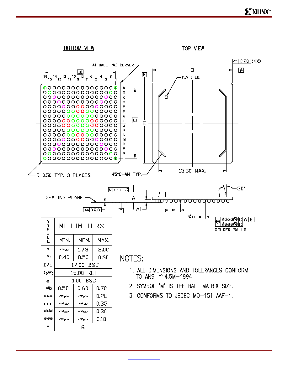
FG256 Fine-Pitch BGA Package
R
14
www.xilinx.com
DS083-4 (v2.5.5) August 25, 2003
1-800-255-7778
Advance Product Specification
FG256 Fine-Pitch BGA Package Specifications (1.00mm pitch)
Figure 1: FG256 Fine-Pitch BGA Package Specifications
Virtex-II ProTM Platform FPGAs: Pinout Information
R
DS083-4 (v2.5.5) August 25, 2003
www.xilinx.com
15
Advance Product Specification
1-800-255-7778
FG456 Fine-Pitch BGA Package
As shown in
Table 6
, XC2VP2, XC2VP4, and XC2VP7 Virtex-II Pro devices are available in the FG456 fine-pitch BGA
package. The pins in these devices are same, except for the differences shown in the "No Connects" column. Following this
table are the
FG456 Fine-Pitch BGA Package Specifications (1.00mm pitch)
.
Table 6: FG456 -- XC2VP2, XC2VP4, and XC2VP7
Bank
Pin Description
Pin Number
No Connects
XC2VP2
XC2VP4
XC2VP7
0
IO_L01N_0/VRP_0
D5
0
IO_L01P_0/VRN_0
D6
0
IO_L02N_0
E6
0
IO_L02P_0
E7
0
IO_L03N_0
D7
0
IO_L03P_0/VREF_0
C7
0
IO_L05_0/No_Pair
E8
0
IO_L06N_0
D8
0
IO_L06P_0
C8
0
IO_L07N_0
F9
0
IO_L07P_0
E9
0
IO_L09N_0
D9
0
IO_L09P_0/VREF_0
D10
0
IO_L67N_0
F10
0
IO_L67P_0
E10
0
IO_L69N_0
C10
0
IO_L69P_0/VREF_0
B11
0
IO_L74N_0/GCLK7P
F11
0
IO_L74P_0/GCLK6S
E11
0
IO_L75N_0/GCLK5P
D11
0
IO_L75P_0/GCLK4S
C11
1
IO_L75N_1/GCLK3P
C12
1
IO_L75P_1/GCLK2S
D12
1
IO_L74N_1/GCLK1P
E12
1
IO_L74P_1/GCLK0S
F12
1
IO_L69N_1/VREF_1
B12
1
IO_L69P_1
C13
1
IO_L67N_1
E13
1
IO_L67P_1
F13
1
IO_L09N_1/VREF_1
D13
1
IO_L09P_1
D14
1
IO_L07N_1
E14
FG456 Fine-Pitch BGA Package
R
16
www.xilinx.com
DS083-4 (v2.5.5) August 25, 2003
1-800-255-7778
Advance Product Specification
1
IO_L07P_1
F14
1
IO_L06N_1
C15
1
IO_L06P_1
D15
1
IO_L05_1/No_Pair
E15
1
IO_L03N_1/VREF_1
C16
1
IO_L03P_1
D16
1
IO_L02N_1
E16
1
IO_L02P_1
E17
1
IO_L01N_1/VRP_1
D17
1
IO_L01P_1/VRN_1
D18
2
IO_L01N_2/VRP_2
C21
2
IO_L01P_2/VRN_2
C22
2
IO_L02N_2
D21
2
IO_L02P_2
D22
2
IO_L03N_2
E19
2
IO_L03P_2
E20
2
IO_L04N_2/VREF_2
E21
2
IO_L04P_2
E22
2
IO_L06N_2
F19
2
IO_L06P_2
F20
2
IO_L43N_2
F21
NC
2
IO_L43P_2
F22
NC
2
IO_L46N_2/VREF_2
F18
NC
2
IO_L46P_2
G18
NC
2
IO_L48N_2
G19
NC
2
IO_L48P_2
G20
NC
2
IO_L49N_2
G21
NC
2
IO_L49P_2
G22
NC
2
IO_L50N_2
H19
NC
2
IO_L50P_2
H20
NC
2
IO_L52N_2/VREF_2
H21
NC
2
IO_L52P_2
H22
NC
2
IO_L54N_2
H18
NC
2
IO_L54P_2
J17
NC
2
IO_L55N_2
J19
NC
2
IO_L55P_2
J20
NC
Table 6: FG456 -- XC2VP2, XC2VP4, and XC2VP7
Bank
Pin Description
Pin Number
No Connects
XC2VP2
XC2VP4
XC2VP7
Virtex-II ProTM Platform FPGAs: Pinout Information
R
DS083-4 (v2.5.5) August 25, 2003
www.xilinx.com
17
Advance Product Specification
1-800-255-7778
2
IO_L56N_2
J21
NC
2
IO_L56P_2
J22
NC
2
IO_L58N_2/VREF_2
J18
NC
2
IO_L58P_2
K18
NC
2
IO_L60N_2
K19
NC
2
IO_L60P_2
K20
NC
2
IO_L85N_2
K21
2
IO_L85P_2
K22
2
IO_L86N_2
K17
2
IO_L86P_2
L17
2
IO_L88N_2/VREF_2
L18
2
IO_L88P_2
L19
2
IO_L90N_2
L20
2
IO_L90P_2
L21
3
IO_L90N_3
M21
3
IO_L90P_3
M20
3
IO_L89N_3
M19
3
IO_L89P_3
M18
3
IO_L87N_3/VREF_3
M17
3
IO_L87P_3
N17
3
IO_L85N_3
N22
3
IO_L85P_3
N21
3
IO_L60N_3
N20
NC
3
IO_L60P_3
N19
NC
3
IO_L59N_3
N18
NC
3
IO_L59P_3
P18
NC
3
IO_L57N_3/VREF_3
P22
NC
3
IO_L57P_3
P21
NC
3
IO_L55N_3
P20
NC
3
IO_L55P_3
P19
NC
3
IO_L54N_3
P17
NC
3
IO_L54P_3
R18
NC
3
IO_L53N_3
R22
NC
3
IO_L53P_3
R21
NC
3
IO_L51N_3/VREF_3
R20
NC
3
IO_L51P_3
R19
NC
Table 6: FG456 -- XC2VP2, XC2VP4, and XC2VP7
Bank
Pin Description
Pin Number
No Connects
XC2VP2
XC2VP4
XC2VP7
FG456 Fine-Pitch BGA Package
R
18
www.xilinx.com
DS083-4 (v2.5.5) August 25, 2003
1-800-255-7778
Advance Product Specification
3
IO_L49N_3
T22
NC
3
IO_L49P_3
T21
NC
3
IO_L48N_3
T20
NC
3
IO_L48P_3
T19
NC
3
IO_L47N_3
T18
NC
3
IO_L47P_3
U18
NC
3
IO_L45N_3/VREF_3
U22
NC
3
IO_L45P_3
U21
NC
3
IO_L43N_3
U20
NC
3
IO_L43P_3
U19
NC
3
IO_L06N_3
V22
3
IO_L06P_3
V21
3
IO_L05N_3
V20
3
IO_L05P_3
V19
3
IO_L03N_3/VREF_3
W22
3
IO_L03P_3
W21
3
IO_L02N_3
Y22
3
IO_L02P_3
Y21
3
IO_L01N_3/VRP_3
AA22
3
IO_L01P_3/VRN_3
AB21
4
IO_L01N_4/BUSY/DOUT
(1)
W18
4
IO_L01P_4/INIT_B
W17
4
IO_L02N_4/D0/DIN
(1)
V17
4
IO_L02P_4/D1
V16
4
IO_L03N_4/D2
W16
4
IO_L03P_4/D3
Y16
4
IO_L05_4/No_Pair
V15
4
IO_L06N_4/VRP_4
W15
4
IO_L06P_4/VRN_4
Y15
4
IO_L07N_4
U14
4
IO_L07P_4/VREF_4
V14
4
IO_L09N_4
W14
4
IO_L09P_4/VREF_4
W13
4
IO_L67N_4
U13
4
IO_L67P_4
V13
4
IO_L69N_4
Y13
Table 6: FG456 -- XC2VP2, XC2VP4, and XC2VP7
Bank
Pin Description
Pin Number
No Connects
XC2VP2
XC2VP4
XC2VP7
Virtex-II ProTM Platform FPGAs: Pinout Information
R
DS083-4 (v2.5.5) August 25, 2003
www.xilinx.com
19
Advance Product Specification
1-800-255-7778
4
IO_L69P_4/VREF_4
AA12
4
IO_L74N_4/GCLK3S
U12
4
IO_L74P_4/GCLK2P
V12
4
IO_L75N_4/GCLK1S
W12
4
IO_L75P_4/GCLK0P
Y12
5
IO_L75N_5/GCLK7S
Y11
5
IO_L75P_5/GCLK6P
W11
5
IO_L74N_5/GCLK5S
V11
5
IO_L74P_5/GCLK4P
U11
5
IO_L69N_5/VREF_5
AA11
5
IO_L69P_5
Y10
5
IO_L67N_5
V10
5
IO_L67P_5
U10
5
IO_L09N_5/VREF_5
W10
5
IO_L09P_5
W9
5
IO_L07N_5/VREF_5
V9
5
IO_L07P_5
U9
5
IO_L06N_5/VRP_5
Y8
5
IO_L06P_5/VRN_5
W8
5
IO_L05_5/No_Pair
V8
5
IO_L03N_5/D4
Y7
5
IO_L03P_5/D5
W7
5
IO_L02N_5/D6
V7
5
IO_L02P_5/D7
V6
5
IO_L01N_5/RDWR_B
W6
5
IO_L01P_5/CS_B
W5
6
IO_L01P_6/VRN_6
AB2
6
IO_L01N_6/VRP_6
AA1
6
IO_L02P_6
Y2
6
IO_L02N_6
Y1
6
IO_L03P_6
W2
6
IO_L03N_6/VREF_6
W1
6
IO_L05P_6
V4
6
IO_L05N_6
V3
6
IO_L06P_6
V2
Table 6: FG456 -- XC2VP2, XC2VP4, and XC2VP7
Bank
Pin Description
Pin Number
No Connects
XC2VP2
XC2VP4
XC2VP7
FG456 Fine-Pitch BGA Package
R
20
www.xilinx.com
DS083-4 (v2.5.5) August 25, 2003
1-800-255-7778
Advance Product Specification
6
IO_L06N_6
V1
6
IO_L43P_6
U4
NC
6
IO_L43N_6
U3
NC
6
IO_L45P_6
U2
NC
6
IO_L45N_6/VREF_6
U1
NC
6
IO_L47P_6
U5
NC
6
IO_L47N_6
T5
NC
6
IO_L48P_6
T4
NC
6
IO_L48N_6
T3
NC
6
IO_L49P_6
T2
NC
6
IO_L49N_6
T1
NC
6
IO_L51P_6
R4
NC
6
IO_L51N_6/VREF_6
R3
NC
6
IO_L53P_6
R2
NC
6
IO_L53N_6
R1
NC
6
IO_L54P_6
R5
NC
6
IO_L54N_6
P6
NC
6
IO_L55P_6
P4
NC
6
IO_L55N_6
P3
NC
6
IO_L57P_6
P2
NC
6
IO_L57N_6/VREF_6
P1
NC
6
IO_L59P_6
P5
NC
6
IO_L59N_6
N5
NC
6
IO_L60P_6
N4
NC
6
IO_L60N_6
N3
NC
6
IO_L85P_6
N2
6
IO_L85N_6
N1
6
IO_L87P_6
N6
6
IO_L87N_6/VREF_6
M6
6
IO_L89P_6
M5
6
IO_L89N_6
M4
6
IO_L90P_6
M3
6
IO_L90N_6
M2
7
IO_L90P_7
L2
7
IO_L90N_7
L3
7
IO_L88P_7
L4
Table 6: FG456 -- XC2VP2, XC2VP4, and XC2VP7
Bank
Pin Description
Pin Number
No Connects
XC2VP2
XC2VP4
XC2VP7

Virtex-II ProTM Platform FPGAs: Pinout Information
R
DS083-4 (v2.5.5) August 25, 2003
www.xilinx.com
21
Advance Product Specification
1-800-255-7778
7
IO_L88N_7/VREF_7
L5
7
IO_L86P_7
L6
7
IO_L86N_7
K6
7
IO_L85P_7
K1
7
IO_L85N_7
K2
7
IO_L60P_7
K3
NC
7
IO_L60N_7
K4
NC
7
IO_L58P_7
K5
NC
7
IO_L58N_7/VREF_7
J5
NC
7
IO_L56P_7
J1
NC
7
IO_L56N_7
J2
NC
7
IO_L55P_7
J3
NC
7
IO_L55N_7
J4
NC
7
IO_L54P_7
J6
NC
7
IO_L54N_7
H5
NC
7
IO_L52P_7
H1
NC
7
IO_L52N_7/VREF_7
H2
NC
7
IO_L50P_7
H3
NC
7
IO_L50N_7
H4
NC
7
IO_L49P_7
G1
NC
7
IO_L49N_7
G2
NC
7
IO_L48P_7
G3
NC
7
IO_L48N_7
G4
NC
7
IO_L46P_7
G5
NC
7
IO_L46N_7/VREF_7
F5
NC
7
IO_L43P_7
F1
NC
7
IO_L43N_7
F2
NC
7
IO_L06P_7
F3
7
IO_L06N_7
F4
7
IO_L04P_7
E1
7
IO_L04N_7/VREF_7
E2
7
IO_L03P_7
E3
7
IO_L03N_7
E4
7
IO_L02P_7
D1
7
IO_L02N_7
D2
7
IO_L01P_7/VRN_7
C1
7
IO_L01N_7/VRP_7
C2
Table 6: FG456 -- XC2VP2, XC2VP4, and XC2VP7
Bank
Pin Description
Pin Number
No Connects
XC2VP2
XC2VP4
XC2VP7
FG456 Fine-Pitch BGA Package
R
22
www.xilinx.com
DS083-4 (v2.5.5) August 25, 2003
1-800-255-7778
Advance Product Specification
0
VCCO_0
G9
0
VCCO_0
G11
0
VCCO_0
G10
0
VCCO_0
F8
0
VCCO_0
F7
1
VCCO_1
G14
1
VCCO_1
G13
1
VCCO_1
G12
1
VCCO_1
F16
1
VCCO_1
F15
2
VCCO_2
L16
2
VCCO_2
K16
2
VCCO_2
J16
2
VCCO_2
H17
2
VCCO_2
G17
3
VCCO_3
T17
3
VCCO_3
R17
3
VCCO_3
P16
3
VCCO_3
N16
3
VCCO_3
M16
4
VCCO_4
U16
4
VCCO_4
U15
4
VCCO_4
T14
4
VCCO_4
T13
4
VCCO_4
T12
5
VCCO_5
U8
5
VCCO_5
U7
5
VCCO_5
T9
5
VCCO_5
T11
5
VCCO_5
T10
6
VCCO_6
T6
6
VCCO_6
R6
6
VCCO_6
P7
6
VCCO_6
N7
6
VCCO_6
M7
7
VCCO_7
L7
Table 6: FG456 -- XC2VP2, XC2VP4, and XC2VP7
Bank
Pin Description
Pin Number
No Connects
XC2VP2
XC2VP4
XC2VP7
Virtex-II ProTM Platform FPGAs: Pinout Information
R
DS083-4 (v2.5.5) August 25, 2003
www.xilinx.com
23
Advance Product Specification
1-800-255-7778
7
VCCO_7
K7
7
VCCO_7
J7
7
VCCO_7
H6
7
VCCO_7
G6
N/A
CCLK
W20
N/A
PROG_B
B1
N/A
DONE
Y18
N/A
M0
Y4
N/A
M1
W3
N/A
M2
Y5
N/A
TCK
B22
N/A
TDI
D3
N/A
TDO
D20
N/A
TMS
A21
N/A
PWRDWN_B
Y19
N/A
HSWAP_EN
A2
N/A
RSVD
C18
N/A
VBATT
C19
N/A
DXP
C4
N/A
DXN
C5
N/A
AVCCAUXTX4
B4
NC
NC
N/A
VTTXPAD4
B3
NC
NC
N/A
TXNPAD4
A3
NC
NC
N/A
TXPPAD4
A4
NC
NC
N/A
GNDA4
C6
NC
NC
N/A
RXPPAD4
A5
NC
NC
N/A
RXNPAD4
A6
NC
NC
N/A
VTRXPAD4
B5
NC
NC
N/A
AVCCAUXRX4
B6
NC
NC
N/A
AVCCAUXTX6
B8
N/A
VTTXPAD6
B7
N/A
TXNPAD6
A7
N/A
TXPPAD6
A8
N/A
GNDA6
C9
N/A
RXPPAD6
A9
N/A
RXNPAD6
A10
Table 6: FG456 -- XC2VP2, XC2VP4, and XC2VP7
Bank
Pin Description
Pin Number
No Connects
XC2VP2
XC2VP4
XC2VP7
FG456 Fine-Pitch BGA Package
R
24
www.xilinx.com
DS083-4 (v2.5.5) August 25, 2003
1-800-255-7778
Advance Product Specification
N/A
VTRXPAD6
B9
N/A
AVCCAUXRX6
B10
N/A
AVCCAUXTX7
B14
N/A
VTTXPAD7
B13
N/A
TXNPAD7
A13
N/A
TXPPAD7
A14
N/A
GNDA7
C14
N/A
RXPPAD7
A15
N/A
RXNPAD7
A16
N/A
VTRXPAD7
B15
N/A
AVCCAUXRX7
B16
N/A
AVCCAUXTX9
B18
NC
NC
N/A
VTTXPAD9
B17
NC
NC
N/A
TXNPAD9
A17
NC
NC
N/A
TXPPAD9
A18
NC
NC
N/A
GNDA9
C17
NC
NC
N/A
RXPPAD9
A19
NC
NC
N/A
RXNPAD9
A20
NC
NC
N/A
VTRXPAD9
B19
NC
NC
N/A
AVCCAUXRX9
B20
NC
NC
N/A
AVCCAUXRX16
AA20
NC
NC
N/A
VTRXPAD16
AA19
NC
NC
N/A
RXNPAD16
AB20
NC
NC
N/A
RXPPAD16
AB19
NC
NC
N/A
GNDA16
Y17
NC
NC
N/A
TXPPAD16
AB18
NC
NC
N/A
TXNPAD16
AB17
NC
NC
N/A
VTTXPAD16
AA17
NC
NC
N/A
AVCCAUXTX16
AA18
NC
NC
N/A
AVCCAUXRX18
AA16
N/A
VTRXPAD18
AA15
N/A
RXNPAD18
AB16
N/A
RXPPAD18
AB15
N/A
GNDA18
Y14
N/A
TXPPAD18
AB14
N/A
TXNPAD18
AB13
N/A
VTTXPAD18
AA13
Table 6: FG456 -- XC2VP2, XC2VP4, and XC2VP7
Bank
Pin Description
Pin Number
No Connects
XC2VP2
XC2VP4
XC2VP7

Virtex-II ProTM Platform FPGAs: Pinout Information
R
DS083-4 (v2.5.5) August 25, 2003
www.xilinx.com
25
Advance Product Specification
1-800-255-7778
N/A
AVCCAUXTX18
AA14
N/A
AVCCAUXRX19
AA10
N/A
VTRXPAD19
AA9
N/A
RXNPAD19
AB10
N/A
RXPPAD19
AB9
N/A
GNDA19
Y9
N/A
TXPPAD19
AB8
N/A
TXNPAD19
AB7
N/A
VTTXPAD19
AA7
N/A
AVCCAUXTX19
AA8
N/A
AVCCAUXRX21
AA6
NC
NC
N/A
VTRXPAD21
AA5
NC
NC
N/A
RXNPAD21
AB6
NC
NC
N/A
RXPPAD21
AB5
NC
NC
N/A
GNDA21
Y6
NC
NC
N/A
TXPPAD21
AB4
NC
NC
N/A
TXNPAD21
AB3
NC
NC
N/A
VTTXPAD21
AA3
NC
NC
N/A
AVCCAUXTX21
AA4
NC
NC
N/A
VCCINT
U6
N/A
VCCINT
U17
N/A
VCCINT
T8
N/A
VCCINT
T7
N/A
VCCINT
T16
N/A
VCCINT
T15
N/A
VCCINT
R7
N/A
VCCINT
R16
N/A
VCCINT
H7
N/A
VCCINT
H16
N/A
VCCINT
G8
N/A
VCCINT
G7
N/A
VCCINT
G16
N/A
VCCINT
G15
N/A
VCCINT
F6
N/A
VCCINT
F17
N/A
VCCAUX
M22
Table 6: FG456 -- XC2VP2, XC2VP4, and XC2VP7
Bank
Pin Description
Pin Number
No Connects
XC2VP2
XC2VP4
XC2VP7
FG456 Fine-Pitch BGA Package
R
26
www.xilinx.com
DS083-4 (v2.5.5) August 25, 2003
1-800-255-7778
Advance Product Specification
N/A
VCCAUX
L1
N/A
VCCAUX
B21
N/A
VCCAUX
B2
N/A
VCCAUX
AB11
N/A
VCCAUX
AA21
N/A
VCCAUX
AA2
N/A
VCCAUX
A12
N/A
GND
Y3
N/A
GND
Y20
N/A
GND
W4
N/A
GND
W19
N/A
GND
V5
N/A
GND
V18
N/A
GND
P9
N/A
GND
P14
N/A
GND
P13
N/A
GND
P12
N/A
GND
P11
N/A
GND
P10
N/A
GND
N9
N/A
GND
N14
N/A
GND
N13
N/A
GND
N12
N/A
GND
N11
N/A
GND
N10
N/A
GND
M9
N/A
GND
M14
N/A
GND
M13
N/A
GND
M12
N/A
GND
M11
N/A
GND
M10
N/A
GND
M1
N/A
GND
L9
N/A
GND
L22
N/A
GND
L14
N/A
GND
L13
N/A
GND
L12
Table 6: FG456 -- XC2VP2, XC2VP4, and XC2VP7
Bank
Pin Description
Pin Number
No Connects
XC2VP2
XC2VP4
XC2VP7

Virtex-II ProTM Platform FPGAs: Pinout Information
R
DS083-4 (v2.5.5) August 25, 2003
www.xilinx.com
27
Advance Product Specification
1-800-255-7778
N/A
GND
L11
N/A
GND
L10
N/A
GND
K9
N/A
GND
K14
N/A
GND
K13
N/A
GND
K12
N/A
GND
K11
N/A
GND
K10
N/A
GND
J9
N/A
GND
J14
N/A
GND
J13
N/A
GND
J12
N/A
GND
J11
N/A
GND
J10
N/A
GND
E5
N/A
GND
E18
N/A
GND
D4
N/A
GND
D19
N/A
GND
C3
N/A
GND
C20
N/A
GND
AB22
N/A
GND
AB12
N/A
GND
AB1
N/A
GND
A22
N/A
GND
A11
N/A
GND
A1
Notes:
1.
See
Table 4
for an explanation of the signals available on this pin.
Table 6: FG456 -- XC2VP2, XC2VP4, and XC2VP7
Bank
Pin Description
Pin Number
No Connects
XC2VP2
XC2VP4
XC2VP7

FG456 Fine-Pitch BGA Package
R
28
www.xilinx.com
DS083-4 (v2.5.5) August 25, 2003
1-800-255-7778
Advance Product Specification
FG456 Fine-Pitch BGA Package Specifications (1.00mm pitch)
Figure 2: FG456 Fine-Pitch BGA Package Specifications
Virtex-II ProTM Platform FPGAs: Pinout Information
R
DS083-4 (v2.5.5) August 25, 2003
www.xilinx.com
29
Advance Product Specification
1-800-255-7778
FG676 Fine-Pitch BGA Package
As shown in
Table 7
, XC2VP20, XC2VP30, and XC2VP40 Virtex-II Pro devices are available in the FG676 fine-pitch BGA
package. The pins in these devices are the same, except for the differences shown in the "No Connects" column. Following
this table are the
FG676 Fine-Pitch BGA Package Specifications (1.00mm pitch)
.
Table 7: FG676 -- XC2VP20, XC2VP30, and XC2VP40
Bank
Pin Description
Pin Number
No Connects
XC2VP20
XC2VP30
XC2VP40
0
IO_L01N_0/VRP_0
E5
0
IO_L01P_0/VRN_0
D5
0
IO_L02N_0
E6
0
IO_L02P_0
D6
0
IO_L03N_0
G7
0
IO_L03P_0/VREF_0
F7
0
IO_L05_0/No_Pair
E7
0
IO_L06N_0
D7
0
IO_L06P_0
C7
0
IO_L07N_0
H8
0
IO_L07P_0
G8
0
IO_L09N_0
F8
0
IO_L09P_0/VREF_0
E8
0
IO_L37N_0
B8
0
IO_L37P_0
A8
0
IO_L39N_0
H9
0
IO_L39P_0
G9
0
IO_L43N_0
F9
0
IO_L43P_0
E9
0
IO_L45N_0
D9
0
IO_L45P_0/VREF_0
C9
0
IO_L46N_0
H10
0
IO_L46P_0
H11
0
IO_L48N_0
E10
0
IO_L48P_0
E11
0
IO_L49N_0
D10
0
IO_L49P_0
C10
0
IO_L50_0/No_Pair
G11
0
IO_L53_0/No_Pair
F11
0
IO_L54N_0
J12
0
IO_L54P_0
H12
FG676 Fine-Pitch BGA Package
R
30
www.xilinx.com
DS083-4 (v2.5.5) August 25, 2003
1-800-255-7778
Advance Product Specification
0
IO_L55N_0
G12
0
IO_L55P_0
F12
0
IO_L57N_0
E12
0
IO_L57P_0/VREF_0
F13
0
IO_L67N_0
D12
0
IO_L67P_0
C12
0
IO_L69N_0
J13
0
IO_L69P_0/VREF_0
H13
0
IO_L74N_0/GCLK7P
E13
0
IO_L74P_0/GCLK6S
D13
0
IO_L75N_0/GCLK5P
C13
0
IO_L75P_0/GCLK4S
B13
1
IO_L75N_1/GCLK3P
B14
1
IO_L75P_1/GCLK2S
C14
1
IO_L74N_1/GCLK1P
D14
1
IO_L74P_1/GCLK0S
E14
1
IO_L69N_1/VREF_1
H14
1
IO_L69P_1
J14
1
IO_L67N_1
C15
1
IO_L67P_1
D15
1
IO_L57N_1/VREF_1
F14
1
IO_L57P_1
E15
1
IO_L55N_1
F15
1
IO_L55P_1
G15
1
IO_L54N_1
H15
1
IO_L54P_1
J15
1
IO_L53_1/No_Pair
F16
1
IO_L50_1/No_Pair
G16
1
IO_L49N_1
C17
1
IO_L49P_1
D17
1
IO_L48N_1
E16
1
IO_L48P_1
E17
1
IO_L46N_1
H16
1
IO_L46P_1
H17
Table 7: FG676 -- XC2VP20, XC2VP30, and XC2VP40
Bank
Pin Description
Pin Number
No Connects
XC2VP20
XC2VP30
XC2VP40
Virtex-II ProTM Platform FPGAs: Pinout Information
R
DS083-4 (v2.5.5) August 25, 2003
www.xilinx.com
31
Advance Product Specification
1-800-255-7778
1
IO_L45N_1/VREF_1
C18
1
IO_L45P_1
D18
1
IO_L43N_1
E18
1
IO_L43P_1
F18
1
IO_L39N_1
G18
1
IO_L39P_1
H18
1
IO_L37N_1
A19
1
IO_L37P_1
B19
1
IO_L09N_1/VREF_1
E19
1
IO_L09P_1
F19
1
IO_L07N_1
G19
1
IO_L07P_1
H19
1
IO_L06N_1
C20
1
IO_L06P_1
D20
1
IO_L05_1/No_Pair
E20
1
IO_L03N_1/VREF_1
F20
1
IO_L03P_1
G20
1
IO_L02N_1
D21
1
IO_L02P_1
E21
1
IO_L01N_1/VRP_1
D22
1
IO_L01P_1/VRN_1
E22
2
IO_L01N_2/VRP_2
C25
2
IO_L01P_2/VRN_2
C26
2
IO_L02N_2
D25
2
IO_L02P_2
D26
2
IO_L03N_2
E23
2
IO_L03P_2
F22
2
IO_L04N_2/VREF_2
E25
2
IO_L04P_2
E26
2
IO_L06N_2
F21
2
IO_L06P_2
G21
2
IO_L24N_2
F23
NC
2
IO_L24P_2
F24
NC
2
IO_L31N_2
F25
Table 7: FG676 -- XC2VP20, XC2VP30, and XC2VP40
Bank
Pin Description
Pin Number
No Connects
XC2VP20
XC2VP30
XC2VP40

FG676 Fine-Pitch BGA Package
R
32
www.xilinx.com
DS083-4 (v2.5.5) August 25, 2003
1-800-255-7778
Advance Product Specification
2
IO_L31P_2
F26
2
IO_L32N_2
G22
2
IO_L32P_2
H22
2
IO_L34N_2/VREF_2
G23
2
IO_L34P_2
G24
2
IO_L36N_2
G25
2
IO_L36P_2
G26
2
IO_L37N_2
H20
2
IO_L37P_2
H21
2
IO_L38N_2
H25
2
IO_L38P_2
H26
2
IO_L40N_2/VREF_2
J19
2
IO_L40P_2
J20
2
IO_L42N_2
J21
2
IO_L42P_2
J22
2
IO_L43N_2
J23
2
IO_L43P_2
J24
2
IO_L44N_2
J25
2
IO_L44P_2
J26
2
IO_L46N_2/VREF_2
K19
2
IO_L46P_2
L19
2
IO_L48N_2
K22
2
IO_L48P_2
K23
2
IO_L49N_2
K24
2
IO_L49P_2
L24
2
IO_L50N_2
K25
2
IO_L50P_2
K26
2
IO_L52N_2/VREF_2
L20
2
IO_L52P_2
M20
2
IO_L54N_2
L21
2
IO_L54P_2
L22
2
IO_L55N_2
L25
2
IO_L55P_2
L26
2
IO_L56N_2
M18
2
IO_L56P_2
M19
Table 7: FG676 -- XC2VP20, XC2VP30, and XC2VP40
Bank
Pin Description
Pin Number
No Connects
XC2VP20
XC2VP30
XC2VP40

Virtex-II ProTM Platform FPGAs: Pinout Information
R
DS083-4 (v2.5.5) August 25, 2003
www.xilinx.com
33
Advance Product Specification
1-800-255-7778
2
IO_L58N_2/VREF_2
M21
2
IO_L58P_2
N21
2
IO_L60N_2
M22
2
IO_L60P_2
M23
2
IO_L85N_2
M25
2
IO_L85P_2
M26
2
IO_L86N_2
N18
2
IO_L86P_2
N19
2
IO_L88N_2/VREF_2
N22
2
IO_L88P_2
N23
2
IO_L90N_2
N24
2
IO_L90P_2
N25
3
IO_L90N_3
P25
3
IO_L90P_3
P24
3
IO_L89N_3
P23
3
IO_L89P_3
P22
3
IO_L87N_3/VREF_3
P19
3
IO_L87P_3
P18
3
IO_L85N_3
R26
3
IO_L85P_3
R25
3
IO_L60N_3
R23
3
IO_L60P_3
R22
3
IO_L59N_3
P21
3
IO_L59P_3
R21
3
IO_L57N_3/VREF_3
R19
3
IO_L57P_3
R18
3
IO_L55N_3
T26
3
IO_L55P_3
T25
3
IO_L54N_3
T22
3
IO_L54P_3
T21
3
IO_L53N_3
R20
3
IO_L53P_3
T20
3
IO_L51N_3/VREF_3
U26
3
IO_L51P_3
U25
Table 7: FG676 -- XC2VP20, XC2VP30, and XC2VP40
Bank
Pin Description
Pin Number
No Connects
XC2VP20
XC2VP30
XC2VP40
FG676 Fine-Pitch BGA Package
R
34
www.xilinx.com
DS083-4 (v2.5.5) August 25, 2003
1-800-255-7778
Advance Product Specification
3
IO_L49N_3
T24
3
IO_L49P_3
U24
3
IO_L48N_3
U23
3
IO_L48P_3
U22
3
IO_L47N_3
T19
3
IO_L47P_3
U19
3
IO_L45N_3/VREF_3
V26
3
IO_L45P_3
V25
3
IO_L43N_3
V24
3
IO_L43P_3
V23
3
IO_L42N_3
V22
3
IO_L42P_3
V21
3
IO_L41N_3
V20
3
IO_L41P_3
V19
3
IO_L39N_3/VREF_3
W26
3
IO_L39P_3
W25
3
IO_L37N_3
W21
3
IO_L37P_3
W20
3
IO_L36N_3
Y26
3
IO_L36P_3
Y25
3
IO_L35N_3
Y24
3
IO_L35P_3
Y23
3
IO_L33N_3/VREF_3
W22
3
IO_L33P_3
Y22
3
IO_L31N_3
AA26
3
IO_L31P_3
AA25
3
IO_L24N_3
AA24
NC
3
IO_L24P_3
AA23
NC
3
IO_L23N_3
Y21
NC
3
IO_L23P_3
AA21
NC
3
IO_L06N_3
AB26
3
IO_L06P_3
AB25
3
IO_L05N_3
AA22
3
IO_L05P_3
AB23
3
IO_L03N_3/VREF_3
AC26
Table 7: FG676 -- XC2VP20, XC2VP30, and XC2VP40
Bank
Pin Description
Pin Number
No Connects
XC2VP20
XC2VP30
XC2VP40
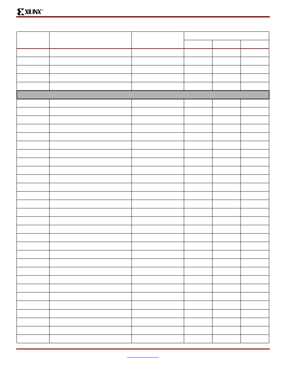
Virtex-II ProTM Platform FPGAs: Pinout Information
R
DS083-4 (v2.5.5) August 25, 2003
www.xilinx.com
35
Advance Product Specification
1-800-255-7778
3
IO_L03P_3
AC25
3
IO_L02N_3
AC24
3
IO_L02P_3
AD25
3
IO_L01N_3/VRP_3
AD26
3
IO_L01P_3/VRN_3
AE26
4
IO_L01N_4/BUSY/DOUT
(1)
AB22
4
IO_L01P_4/INIT_B
AC22
4
IO_L02N_4/D0/DIN
(1)
AB21
4
IO_L02P_4/D1
AC21
4
IO_L03N_4/D2
Y20
4
IO_L03P_4/D3
AA20
4
IO_L05_4/No_Pair
AB20
4
IO_L06N_4/VRP_4
AC20
4
IO_L06P_4/VRN_4
AD20
4
IO_L07N_4
W19
4
IO_L07P_4/VREF_4
Y19
4
IO_L09N_4
AA19
4
IO_L09P_4/VREF_4
AB19
4
IO_L37N_4
AE19
4
IO_L37P_4
AF19
4
IO_L39N_4
W18
4
IO_L39P_4
Y18
4
IO_L43N_4
AA18
4
IO_L43P_4
AB18
4
IO_L45N_4
AC18
4
IO_L45P_4/VREF_4
AD18
4
IO_L46N_4
W17
4
IO_L46P_4
W16
4
IO_L48N_4
AB17
4
IO_L48P_4
AB16
4
IO_L49N_4
AC17
4
IO_L49P_4
AD17
4
IO_L50_4/No_Pair
Y16
4
IO_L53_4/No_Pair
AA16
Table 7: FG676 -- XC2VP20, XC2VP30, and XC2VP40
Bank
Pin Description
Pin Number
No Connects
XC2VP20
XC2VP30
XC2VP40

FG676 Fine-Pitch BGA Package
R
36
www.xilinx.com
DS083-4 (v2.5.5) August 25, 2003
1-800-255-7778
Advance Product Specification
4
IO_L54N_4
V15
4
IO_L54P_4
W15
4
IO_L55N_4
Y15
4
IO_L55P_4
AA15
4
IO_L57N_4
AB15
4
IO_L57P_4/VREF_4
AA14
4
IO_L67N_4
AC15
4
IO_L67P_4
AD15
4
IO_L69N_4
V14
4
IO_L69P_4/VREF_4
W14
4
IO_L74N_4/GCLK3S
AB14
4
IO_L74P_4/GCLK2P
AC14
4
IO_L75N_4/GCLK1S
AD14
4
IO_L75P_4/GCLK0P
AE14
5
IO_L75N_5/GCLK7S
AE13
5
IO_L75P_5/GCLK6P
AD13
5
IO_L74N_5/GCLK5S
AC13
5
IO_L74P_5/GCLK4P
AB13
5
IO_L69N_5/VREF_5
W13
5
IO_L69P_5
V13
5
IO_L67N_5
AD12
5
IO_L67P_5
AC12
5
IO_L57N_5/VREF_5
AA13
5
IO_L57P_5
AB12
5
IO_L55N_5
AA12
5
IO_L55P_5
Y12
5
IO_L54N_5
W12
5
IO_L54P_5
V12
5
IO_L53_5/No_Pair
AA11
5
IO_L50_5/No_Pair
Y11
5
IO_L49N_5
AD10
5
IO_L49P_5
AC10
5
IO_L48N_5
AB11
5
IO_L48P_5
AB10
Table 7: FG676 -- XC2VP20, XC2VP30, and XC2VP40
Bank
Pin Description
Pin Number
No Connects
XC2VP20
XC2VP30
XC2VP40
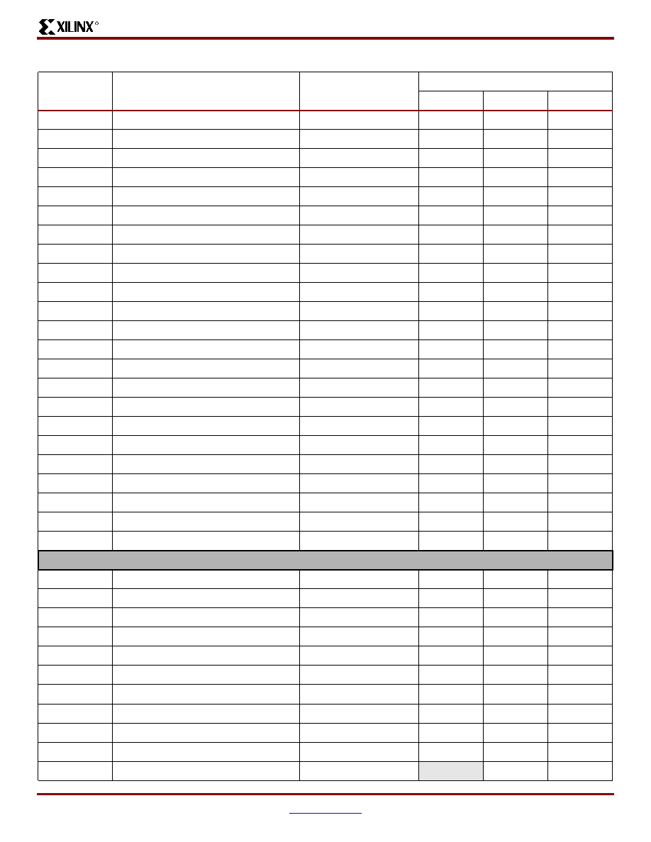
Virtex-II ProTM Platform FPGAs: Pinout Information
R
DS083-4 (v2.5.5) August 25, 2003
www.xilinx.com
37
Advance Product Specification
1-800-255-7778
5
IO_L46N_5
W11
5
IO_L46P_5
W10
5
IO_L45N_5/VREF_5
AD9
5
IO_L45P_5
AC9
5
IO_L43N_5
AB9
5
IO_L43P_5
AA9
5
IO_L39N_5
Y9
5
IO_L39P_5
W9
5
IO_L37N_5
AF8
5
IO_L37P_5
AE8
5
IO_L09N_5/VREF_5
AB8
5
IO_L09P_5
AA8
5
IO_L07N_5/VREF_5
Y8
5
IO_L07P_5
W8
5
IO_L06N_5/VRP_5
AD7
5
IO_L06P_5/VRN_5
AC7
5
IO_L05_5/No_Pair
AB7
5
IO_L03N_5/D4
AA7
5
IO_L03P_5/D5
Y7
5
IO_L02N_5/D6
AC6
5
IO_L02P_5/D7
AB6
5
IO_L01N_5/RDWR_B
AC5
5
IO_L01P_5/CS_B
AB5
6
IO_L01P_6/VRN_6
AE1
6
IO_L01N_6/VRP_6
AD1
6
IO_L02P_6
AD2
6
IO_L02N_6
AC3
6
IO_L03P_6
AC2
6
IO_L03N_6/VREF_6
AC1
6
IO_L05P_6
AB4
6
IO_L05N_6
AA5
6
IO_L06P_6
AB2
6
IO_L06N_6
AB1
6
IO_L23P_6
AA6
NC
Table 7: FG676 -- XC2VP20, XC2VP30, and XC2VP40
Bank
Pin Description
Pin Number
No Connects
XC2VP20
XC2VP30
XC2VP40
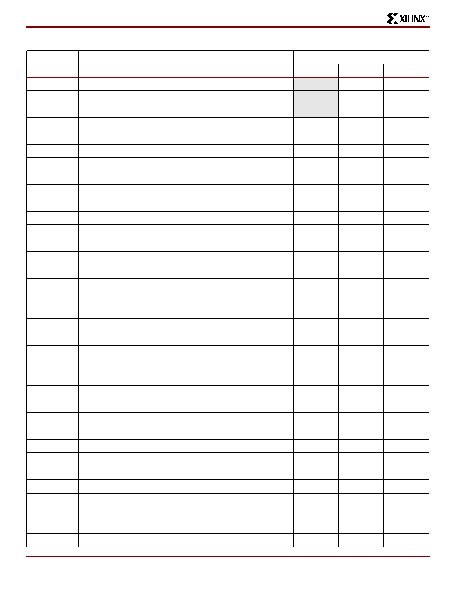
FG676 Fine-Pitch BGA Package
R
38
www.xilinx.com
DS083-4 (v2.5.5) August 25, 2003
1-800-255-7778
Advance Product Specification
6
IO_L23N_6
Y6
NC
6
IO_L24P_6
AA4
NC
6
IO_L24N_6
AA3
NC
6
IO_L31P_6
AA2
6
IO_L31N_6
AA1
6
IO_L33P_6
Y5
6
IO_L33N_6/VREF_6
W5
6
IO_L35P_6
Y4
6
IO_L35N_6
Y3
6
IO_L36P_6
Y2
6
IO_L36N_6
Y1
6
IO_L37P_6
W7
6
IO_L37N_6
W6
6
IO_L39P_6
W2
6
IO_L39N_6/VREF_6
W1
6
IO_L41P_6
V8
6
IO_L41N_6
V7
6
IO_L42P_6
V6
6
IO_L42N_6
V5
6
IO_L43P_6
V4
6
IO_L43N_6
V3
6
IO_L45P_6
V2
6
IO_L45N_6/VREF_6
V1
6
IO_L47P_6
U8
6
IO_L47N_6
T8
6
IO_L48P_6
U5
6
IO_L48N_6
U4
6
IO_L49P_6
U3
6
IO_L49N_6
T3
6
IO_L51P_6
U2
6
IO_L51N_6/VREF_6
U1
6
IO_L53P_6
T7
6
IO_L53N_6
R7
6
IO_L54P_6
T6
6
IO_L54N_6
T5
Table 7: FG676 -- XC2VP20, XC2VP30, and XC2VP40
Bank
Pin Description
Pin Number
No Connects
XC2VP20
XC2VP30
XC2VP40
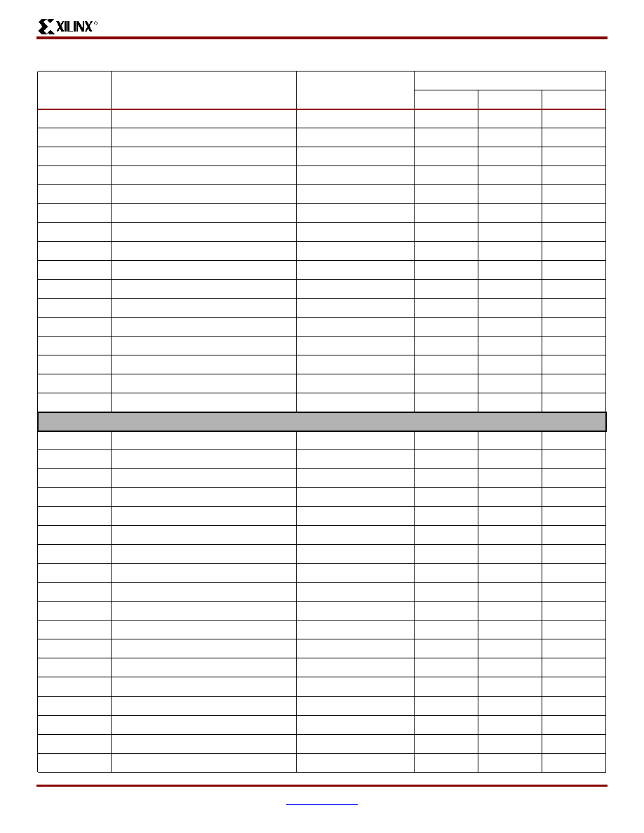
Virtex-II ProTM Platform FPGAs: Pinout Information
R
DS083-4 (v2.5.5) August 25, 2003
www.xilinx.com
39
Advance Product Specification
1-800-255-7778
6
IO_L55P_6
T2
6
IO_L55N_6
T1
6
IO_L57P_6
R9
6
IO_L57N_6/VREF_6
R8
6
IO_L59P_6
R6
6
IO_L59N_6
P6
6
IO_L60P_6
R5
6
IO_L60N_6
R4
6
IO_L85P_6
R2
6
IO_L85N_6
R1
6
IO_L87P_6
P9
6
IO_L87N_6/VREF_6
P8
6
IO_L89P_6
P5
6
IO_L89N_6
P4
6
IO_L90P_6
P3
6
IO_L90N_6
P2
7
IO_L90P_7
N2
7
IO_L90N_7
N3
7
IO_L88P_7
N4
7
IO_L88N_7/VREF_7
N5
7
IO_L86P_7
N8
7
IO_L86N_7
N9
7
IO_L85P_7
M1
7
IO_L85N_7
M2
7
IO_L60P_7
M4
7
IO_L60N_7
M5
7
IO_L58P_7
N6
7
IO_L58N_7/VREF_7
M6
7
IO_L56P_7
M8
7
IO_L56N_7
M9
7
IO_L55P_7
L1
7
IO_L55N_7
L2
7
IO_L54P_7
L5
7
IO_L54N_7
L6
Table 7: FG676 -- XC2VP20, XC2VP30, and XC2VP40
Bank
Pin Description
Pin Number
No Connects
XC2VP20
XC2VP30
XC2VP40
FG676 Fine-Pitch BGA Package
R
40
www.xilinx.com
DS083-4 (v2.5.5) August 25, 2003
1-800-255-7778
Advance Product Specification
7
IO_L52P_7
M7
7
IO_L52N_7/VREF_7
L7
7
IO_L50P_7
K1
7
IO_L50N_7
K2
7
IO_L49P_7
L3
7
IO_L49N_7
K3
7
IO_L48P_7
K4
7
IO_L48N_7
K5
7
IO_L46P_7
L8
7
IO_L46N_7/VREF_7
K8
7
IO_L44P_7
J1
7
IO_L44N_7
J2
7
IO_L43P_7
J3
7
IO_L43N_7
J4
7
IO_L42P_7
J5
7
IO_L42N_7
J6
7
IO_L40P_7
J7
7
IO_L40N_7/VREF_7
J8
7
IO_L38P_7
H1
7
IO_L38N_7
H2
7
IO_L37P_7
H6
7
IO_L37N_7
H7
7
IO_L36P_7
G1
7
IO_L36N_7
G2
7
IO_L34P_7
G3
7
IO_L34N_7/VREF_7
G4
7
IO_L32P_7
H5
7
IO_L32N_7
G5
7
IO_L31P_7
F1
7
IO_L31N_7
F2
7
IO_L24P_7
F3
NC
7
IO_L24N_7
F4
NC
7
IO_L06P_7
G6
7
IO_L06N_7
F6
7
IO_L04P_7
E1
Table 7: FG676 -- XC2VP20, XC2VP30, and XC2VP40
Bank
Pin Description
Pin Number
No Connects
XC2VP20
XC2VP30
XC2VP40

Virtex-II ProTM Platform FPGAs: Pinout Information
R
DS083-4 (v2.5.5) August 25, 2003
www.xilinx.com
41
Advance Product Specification
1-800-255-7778
7
IO_L04N_7/VREF_7
E2
7
IO_L03P_7
F5
7
IO_L03N_7
E4
7
IO_L02P_7
D1
7
IO_L02N_7
D2
7
IO_L01P_7/VRN_7
C1
7
IO_L01N_7/VRP_7
C2
0
VCCO_0
C5
0
VCCO_0
C8
0
VCCO_0
D11
0
VCCO_0
J10
0
VCCO_0
J11
0
VCCO_0
K12
0
VCCO_0
K13
1
VCCO_1
C19
1
VCCO_1
C22
1
VCCO_1
D16
1
VCCO_1
J16
1
VCCO_1
J17
1
VCCO_1
K14
1
VCCO_1
K15
2
VCCO_2
E24
2
VCCO_2
H24
2
VCCO_2
K18
2
VCCO_2
L18
2
VCCO_2
L23
2
VCCO_2
M17
2
VCCO_2
N17
3
VCCO_3
P17
3
VCCO_3
R17
3
VCCO_3
T18
3
VCCO_3
T23
3
VCCO_3
U18
3
VCCO_3
W24
Table 7: FG676 -- XC2VP20, XC2VP30, and XC2VP40
Bank
Pin Description
Pin Number
No Connects
XC2VP20
XC2VP30
XC2VP40
FG676 Fine-Pitch BGA Package
R
42
www.xilinx.com
DS083-4 (v2.5.5) August 25, 2003
1-800-255-7778
Advance Product Specification
3
VCCO_3
AB24
4
VCCO_4
U14
4
VCCO_4
U15
4
VCCO_4
V16
4
VCCO_4
V17
4
VCCO_4
AC16
4
VCCO_4
AD19
4
VCCO_4
AD22
5
VCCO_5
U12
5
VCCO_5
U13
5
VCCO_5
V10
5
VCCO_5
V11
5
VCCO_5
AC11
5
VCCO_5
AD5
5
VCCO_5
AD8
6
VCCO_6
P10
6
VCCO_6
R10
6
VCCO_6
T4
6
VCCO_6
T9
6
VCCO_6
U9
6
VCCO_6
W3
6
VCCO_6
AB3
7
VCCO_7
E3
7
VCCO_7
H3
7
VCCO_7
K9
7
VCCO_7
L4
7
VCCO_7
L9
7
VCCO_7
M10
7
VCCO_7
N10
N/A
PROG_B
B1
N/A
HSWAP_EN
B3
N/A
DXP
A3
N/A
DXN
C4
N/A
AVCCAUXTX4
B5
Table 7: FG676 -- XC2VP20, XC2VP30, and XC2VP40
Bank
Pin Description
Pin Number
No Connects
XC2VP20
XC2VP30
XC2VP40

Virtex-II ProTM Platform FPGAs: Pinout Information
R
DS083-4 (v2.5.5) August 25, 2003
www.xilinx.com
43
Advance Product Specification
1-800-255-7778
N/A
VTTXPAD4
B4
N/A
TXNPAD4
A4
N/A
TXPPAD4
A5
N/A
GNDA4
C6
N/A
RXPPAD4
A6
N/A
RXNPAD4
A7
N/A
VTRXPAD4
B6
N/A
AVCCAUXRX4
B7
N/A
AVCCAUXTX6
B10
N/A
VTTXPAD6
B9
N/A
TXNPAD6
A9
N/A
TXPPAD6
A10
N/A
GNDA6
C11
N/A
RXPPAD6
A11
N/A
RXNPAD6
A12
N/A
VTRXPAD6
B11
N/A
AVCCAUXRX6
B12
N/A
AVCCAUXTX7
B16
N/A
VTTXPAD7
B15
N/A
TXNPAD7
A15
N/A
TXPPAD7
A16
N/A
GNDA7
C16
N/A
RXPPAD7
A17
N/A
RXNPAD7
A18
N/A
VTRXPAD7
B17
N/A
AVCCAUXRX7
B18
N/A
AVCCAUXTX9
B21
N/A
VTTXPAD9
B20
N/A
TXNPAD9
A20
N/A
TXPPAD9
A21
N/A
GNDA9
C21
N/A
RXPPAD9
A22
N/A
RXNPAD9
A23
N/A
VTRXPAD9
B22
N/A
AVCCAUXRX9
B23
Table 7: FG676 -- XC2VP20, XC2VP30, and XC2VP40
Bank
Pin Description
Pin Number
No Connects
XC2VP20
XC2VP30
XC2VP40

FG676 Fine-Pitch BGA Package
R
44
www.xilinx.com
DS083-4 (v2.5.5) August 25, 2003
1-800-255-7778
Advance Product Specification
N/A
RSVD
C23
N/A
VBATT
A24
N/A
TMS
B24
N/A
TCK
B26
N/A
TDO
D24
N/A
CCLK
AE24
N/A
PWRDWN_B
AF24
N/A
DONE
AD23
N/A
AVCCAUXRX16
AE23
N/A
VTRXPAD16
AE22
N/A
RXNPAD16
AF23
N/A
RXPPAD16
AF22
N/A
GNDA16
AD21
N/A
TXPPAD16
AF21
N/A
TXNPAD16
AF20
N/A
VTTXPAD16
AE20
N/A
AVCCAUXTX16
AE21
N/A
AVCCAUXRX18
AE18
N/A
VTRXPAD18
AE17
N/A
RXNPAD18
AF18
N/A
RXPPAD18
AF17
N/A
GNDA18
AD16
N/A
TXPPAD18
AF16
N/A
TXNPAD18
AF15
N/A
VTTXPAD18
AE15
N/A
AVCCAUXTX18
AE16
N/A
AVCCAUXRX19
AE12
N/A
VTRXPAD19
AE11
N/A
RXNPAD19
AF12
N/A
RXPPAD19
AF11
N/A
GNDA19
AD11
N/A
TXPPAD19
AF10
N/A
TXNPAD19
AF9
N/A
VTTXPAD19
AE9
N/A
AVCCAUXTX19
AE10
Table 7: FG676 -- XC2VP20, XC2VP30, and XC2VP40
Bank
Pin Description
Pin Number
No Connects
XC2VP20
XC2VP30
XC2VP40

Virtex-II ProTM Platform FPGAs: Pinout Information
R
DS083-4 (v2.5.5) August 25, 2003
www.xilinx.com
45
Advance Product Specification
1-800-255-7778
N/A
AVCCAUXRX21
AE7
N/A
VTRXPAD21
AE6
N/A
RXNPAD21
AF7
N/A
RXPPAD21
AF6
N/A
GNDA21
AD6
N/A
TXPPAD21
AF5
N/A
TXNPAD21
AF4
N/A
VTTXPAD21
AE4
N/A
AVCCAUXTX21
AE5
N/A
M2
AD4
N/A
M0
AF3
N/A
M1
AE3
N/A
TDI
D3
N/A
VCCINT
G10
N/A
VCCINT
G13
N/A
VCCINT
G14
N/A
VCCINT
G17
N/A
VCCINT
J9
N/A
VCCINT
J18
N/A
VCCINT
K7
N/A
VCCINT
K10
N/A
VCCINT
K11
N/A
VCCINT
K16
N/A
VCCINT
K17
N/A
VCCINT
K20
N/A
VCCINT
L10
N/A
VCCINT
L17
N/A
VCCINT
N7
N/A
VCCINT
N20
N/A
VCCINT
P7
N/A
VCCINT
P20
N/A
VCCINT
T10
N/A
VCCINT
T17
N/A
VCCINT
U7
Table 7: FG676 -- XC2VP20, XC2VP30, and XC2VP40
Bank
Pin Description
Pin Number
No Connects
XC2VP20
XC2VP30
XC2VP40
FG676 Fine-Pitch BGA Package
R
46
www.xilinx.com
DS083-4 (v2.5.5) August 25, 2003
1-800-255-7778
Advance Product Specification
N/A
VCCINT
U10
N/A
VCCINT
U11
N/A
VCCINT
U16
N/A
VCCINT
U17
N/A
VCCINT
U20
N/A
VCCINT
V9
N/A
VCCINT
V18
N/A
VCCINT
Y10
N/A
VCCINT
Y13
N/A
VCCINT
Y14
N/A
VCCINT
Y17
N/A
VCCAUX
A2
N/A
VCCAUX
A13
N/A
VCCAUX
A14
N/A
VCCAUX
A25
N/A
VCCAUX
N1
N/A
VCCAUX
N26
N/A
VCCAUX
P1
N/A
VCCAUX
P26
N/A
VCCAUX
AF2
N/A
VCCAUX
AF13
N/A
VCCAUX
AF14
N/A
VCCAUX
AF25
N/A
GND
A1
N/A
GND
A26
N/A
GND
B2
N/A
GND
B25
N/A
GND
C3
N/A
GND
C24
N/A
GND
D4
N/A
GND
D8
N/A
GND
D19
N/A
GND
D23
N/A
GND
F10
N/A
GND
F17
Table 7: FG676 -- XC2VP20, XC2VP30, and XC2VP40
Bank
Pin Description
Pin Number
No Connects
XC2VP20
XC2VP30
XC2VP40
Virtex-II ProTM Platform FPGAs: Pinout Information
R
DS083-4 (v2.5.5) August 25, 2003
www.xilinx.com
47
Advance Product Specification
1-800-255-7778
N/A
GND
H4
N/A
GND
H23
N/A
GND
K6
N/A
GND
K21
N/A
GND
L11
N/A
GND
L12
N/A
GND
L13
N/A
GND
L14
N/A
GND
L15
N/A
GND
L16
N/A
GND
M3
N/A
GND
M11
N/A
GND
M12
N/A
GND
M13
N/A
GND
M14
N/A
GND
M15
N/A
GND
M16
N/A
GND
M24
N/A
GND
N11
N/A
GND
N12
N/A
GND
N13
N/A
GND
N14
N/A
GND
N15
N/A
GND
N16
N/A
GND
P11
N/A
GND
P12
N/A
GND
P13
N/A
GND
P14
N/A
GND
P15
N/A
GND
P16
N/A
GND
R3
N/A
GND
R11
N/A
GND
R12
N/A
GND
R13
N/A
GND
R14
Table 7: FG676 -- XC2VP20, XC2VP30, and XC2VP40
Bank
Pin Description
Pin Number
No Connects
XC2VP20
XC2VP30
XC2VP40
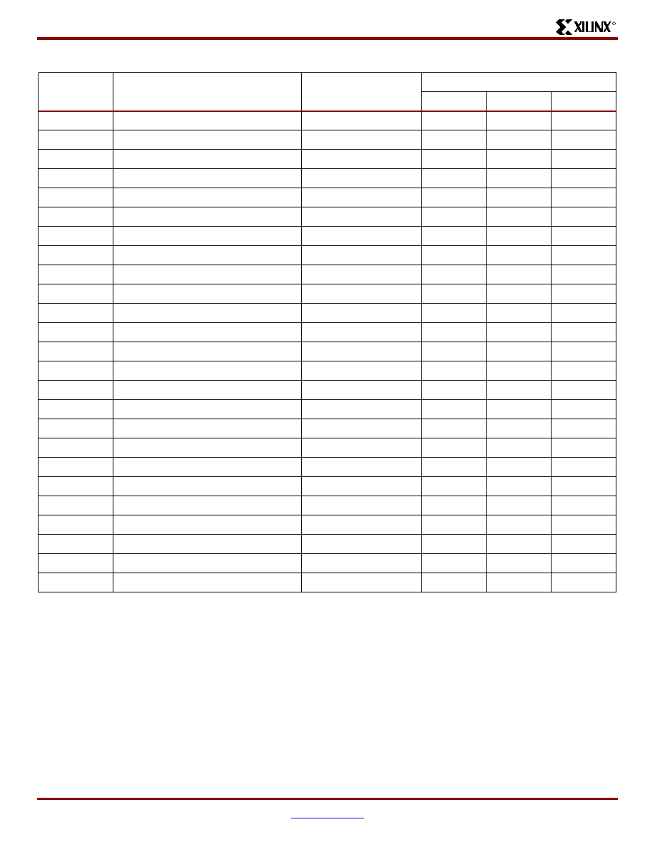
FG676 Fine-Pitch BGA Package
R
48
www.xilinx.com
DS083-4 (v2.5.5) August 25, 2003
1-800-255-7778
Advance Product Specification
N/A
GND
R15
N/A
GND
R16
N/A
GND
R24
N/A
GND
T11
N/A
GND
T12
N/A
GND
T13
N/A
GND
T14
N/A
GND
T15
N/A
GND
T16
N/A
GND
U6
N/A
GND
U21
N/A
GND
W4
N/A
GND
W23
N/A
GND
AA10
N/A
GND
AA17
N/A
GND
AC4
N/A
GND
AC8
N/A
GND
AC19
N/A
GND
AC23
N/A
GND
AD3
N/A
GND
AD24
N/A
GND
AE2
N/A
GND
AE25
N/A
GND
AF1
N/A
GND
AF26
Notes:
1.
See
Table 4
for an explanation of the signals available on this pin.
Table 7: FG676 -- XC2VP20, XC2VP30, and XC2VP40
Bank
Pin Description
Pin Number
No Connects
XC2VP20
XC2VP30
XC2VP40
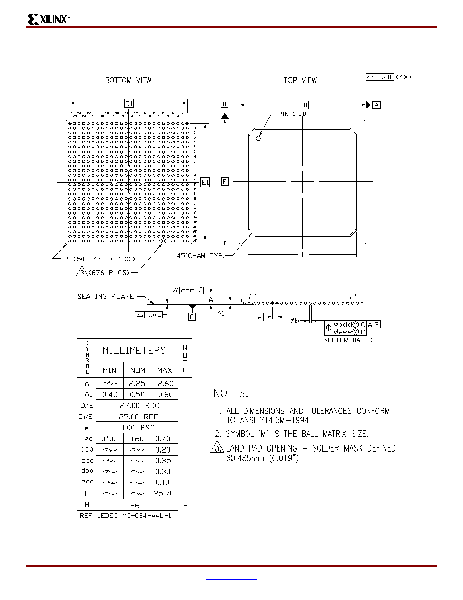
Virtex-II ProTM Platform FPGAs: Pinout Information
R
DS083-4 (v2.5.5) August 25, 2003
www.xilinx.com
49
Advance Product Specification
1-800-255-7778
FG676 Fine-Pitch BGA Package Specifications (1.00mm pitch)
Figure 3: FG676 Fine-Pitch BGA Package Specifications

FF672 Flip-Chip Fine-Pitch BGA Package
R
50
www.xilinx.com
DS083-4 (v2.5.5) August 25, 2003
1-800-255-7778
Advance Product Specification
FF672 Flip-Chip Fine-Pitch BGA Package
As shown in
Table 8
, XC2VP2, XC2VP4, and XC2VP7 Virtex-II Pro devices are available in the FF672 flip-chip fine-pitch
BGA package. Pins in each of these devices are the same, except for differences shown in the "No Connects" column.
Following this table are the
FF672 Flip-Chip Fine-Pitch BGA Package Specifications (1.00mm pitch)
.
Table 8: FF672 -- XC2VP2, XC2VP4, and XC2VP7
Bank
Pin Description
Pin
Number
No Connects
XC2VP2
XC2VP4
XC2VP7
0
IO_L01N_0/VRP_0
B24
0
IO_L01P_0/VRN_0
A24
0
IO_L02N_0
D21
0
IO_L02P_0
C21
0
IO_L03N_0
E20
0
IO_L03P_0/VREF_0
D20
0
IO_L05_0/No_Pair
F19
0
IO_L06N_0
E19
0
IO_L06P_0
E18
0
IO_L07N_0
D19
0
IO_L07P_0
C19
0
IO_L08N_0
B19
0
IO_L08P_0
A19
0
IO_L09N_0
G18
0
IO_L09P_0/VREF_0
F18
0
IO_L37N_0
D18
NC
NC
0
IO_L37P_0
C18
NC
NC
0
IO_L38N_0
G17
NC
NC
0
IO_L38P_0
H16
NC
NC
0
IO_L39N_0
F17
NC
NC
0
IO_L39P_0
F16
NC
NC
0
IO_L43N_0
E17
NC
NC
0
IO_L43P_0
D17
NC
NC
0
IO_L44N_0
G16
NC
NC
0
IO_L44P_0
G15
NC
NC
0
IO_L45N_0
E16
NC
NC
0
IO_L45P_0/VREF_0
D16
NC
NC
0
IO_L67N_0
F15
0
IO_L67P_0
E15
0
IO_L68N_0
D15
0
IO_L68P_0
C15
0
IO_L69N_0
H15
0
IO_L69P_0/VREF_0
H14
Virtex-II ProTM Platform FPGAs: Pinout Information
R
DS083-4 (v2.5.5) August 25, 2003
www.xilinx.com
51
Advance Product Specification
1-800-255-7778
0
IO_L73N_0
G14
0
IO_L73P_0
F14
0
IO_L74N_0/GCLK7P
E14
0
IO_L74P_0/GCLK6S
D14
0
IO_L75N_0/GCLK5P
C14
0
IO_L75P_0/GCLK4S
B14
1
IO_L75N_1/GCLK3P
B13
1
IO_L75P_1/GCLK2S
C13
1
IO_L74N_1/GCLK1P
D13
1
IO_L74P_1/GCLK0S
E13
1
IO_L73N_1
F13
1
IO_L73P_1
G13
1
IO_L69N_1/VREF_1
H13
1
IO_L69P_1
H12
1
IO_L68N_1
C12
1
IO_L68P_1
D12
1
IO_L67N_1
E12
1
IO_L67P_1
F12
1
IO_L45N_1/VREF_1
D11
NC
NC
1
IO_L45P_1
E11
NC
NC
1
IO_L44N_1
G12
NC
NC
1
IO_L44P_1
G11
NC
NC
1
IO_L43N_1
D10
NC
NC
1
IO_L43P_1
E10
NC
NC
1
IO_L39N_1
F11
NC
NC
1
IO_L39P_1
F10
NC
NC
1
IO_L38N_1
H11
NC
NC
1
IO_L38P_1
G10
NC
NC
1
IO_L37N_1
C9
NC
NC
1
IO_L37P_1
D9
NC
NC
1
IO_L09N_1/VREF_1
F9
1
IO_L09P_1
G9
1
IO_L08N_1
A8
1
IO_L08P_1
B8
1
IO_L07N_1
C8
1
IO_L07P_1
D8
Table 8: FF672 -- XC2VP2, XC2VP4, and XC2VP7
Bank
Pin Description
Pin
Number
No Connects
XC2VP2
XC2VP4
XC2VP7

FF672 Flip-Chip Fine-Pitch BGA Package
R
52
www.xilinx.com
DS083-4 (v2.5.5) August 25, 2003
1-800-255-7778
Advance Product Specification
1
IO_L06N_1
E9
1
IO_L06P_1
E8
1
IO_L05_1/No_Pair
F8
1
IO_L03N_1/VREF_1
D7
1
IO_L03P_1
E7
1
IO_L02N_1
C6
1
IO_L02P_1
D6
1
IO_L01N_1/VRP_1
A3
1
IO_L01P_1/VRN_1
B3
2
IO_L01N_2/VRP_2
C4
2
IO_L01P_2/VRN_2
D3
2
IO_L02N_2
A2
2
IO_L02P_2
B1
2
IO_L03N_2
C2
2
IO_L03P_2
C1
2
IO_L04N_2/VREF_2
D2
2
IO_L04P_2
D1
2
IO_L05N_2
E4
2
IO_L05P_2
E3
2
IO_L06N_2
E2
2
IO_L06P_2
E1
2
IO_L40N_2/VREF_2
F5
NC
NC
NC
2
IO_L40P_2
F4
NC
NC
NC
2
IO_L42N_2
F3
NC
NC
NC
2
IO_L42P_2
F2
NC
NC
NC
2
IO_L43N_2
G6
NC
2
IO_L43P_2
G5
NC
2
IO_L44N_2
G4
NC
2
IO_L44P_2
G3
NC
2
IO_L45N_2
F1
NC
2
IO_L45P_2
G1
NC
2
IO_L46N_2/VREF_2
H6
NC
2
IO_L46P_2
H5
NC
2
IO_L47N_2
H4
NC
2
IO_L47P_2
H3
NC
2
IO_L48N_2
H2
NC
Table 8: FF672 -- XC2VP2, XC2VP4, and XC2VP7
Bank
Pin Description
Pin
Number
No Connects
XC2VP2
XC2VP4
XC2VP7
Virtex-II ProTM Platform FPGAs: Pinout Information
R
DS083-4 (v2.5.5) August 25, 2003
www.xilinx.com
53
Advance Product Specification
1-800-255-7778
2
IO_L48P_2
H1
NC
2
IO_L49N_2
J7
NC
2
IO_L49P_2
J6
NC
2
IO_L50N_2
J5
NC
2
IO_L50P_2
J4
NC
2
IO_L51N_2
J3
NC
2
IO_L51P_2
J2
NC
2
IO_L52N_2/VREF_2
K6
NC
2
IO_L52P_2
K5
NC
2
IO_L53N_2
K4
NC
2
IO_L53P_2
K3
NC
2
IO_L54N_2
J1
NC
2
IO_L54P_2
K1
NC
2
IO_L55N_2
K7
NC
2
IO_L55P_2
L8
NC
2
IO_L56N_2
L7
NC
2
IO_L56P_2
M7
NC
2
IO_L57N_2
L6
NC
2
IO_L57P_2
L5
NC
2
IO_L58N_2/VREF_2
L4
NC
2
IO_L58P_2
L3
NC
2
IO_L59N_2
L2
NC
2
IO_L59P_2
L1
NC
2
IO_L60N_2
M8
NC
2
IO_L60P_2
N8
NC
2
IO_L85N_2
M6
2
IO_L85P_2
M5
2
IO_L86N_2
M4
2
IO_L86P_2
M3
2
IO_L87N_2
M2
2
IO_L87P_2
M1
2
IO_L88N_2/VREF_2
N7
2
IO_L88P_2
N6
2
IO_L89N_2
N5
2
IO_L89P_2
N4
2
IO_L90N_2
N3
2
IO_L90P_2
N2
Table 8: FF672 -- XC2VP2, XC2VP4, and XC2VP7
Bank
Pin Description
Pin
Number
No Connects
XC2VP2
XC2VP4
XC2VP7

FF672 Flip-Chip Fine-Pitch BGA Package
R
54
www.xilinx.com
DS083-4 (v2.5.5) August 25, 2003
1-800-255-7778
Advance Product Specification
3
IO_L90N_3
P2
3
IO_L90P_3
P3
3
IO_L89N_3
P4
3
IO_L89P_3
P5
3
IO_L88N_3
P6
3
IO_L88P_3
P7
3
IO_L87N_3/VREF_3
R1
3
IO_L87P_3
R2
3
IO_L86N_3
R3
3
IO_L86P_3
R4
3
IO_L85N_3
R5
3
IO_L85P_3
R6
3
IO_L60N_3
P8
NC
3
IO_L60P_3
R8
NC
3
IO_L59N_3
T1
NC
3
IO_L59P_3
T2
NC
3
IO_L58N_3
T3
NC
3
IO_L58P_3
T4
NC
3
IO_L57N_3/VREF_3
T5
NC
3
IO_L57P_3
T6
NC
3
IO_L56N_3
R7
NC
3
IO_L56P_3
T7
NC
3
IO_L55N_3
T8
NC
3
IO_L55P_3
U7
NC
3
IO_L54N_3
U1
NC
3
IO_L54P_3
V1
NC
3
IO_L53N_3
U3
NC
3
IO_L53P_3
U4
NC
3
IO_L52N_3
U5
NC
3
IO_L52P_3
U6
NC
3
IO_L51N_3/VREF_3
V2
NC
3
IO_L51P_3
V3
NC
3
IO_L50N_3
V4
NC
3
IO_L50P_3
V5
NC
3
IO_L49N_3
V6
NC
3
IO_L49P_3
V7
NC
Table 8: FF672 -- XC2VP2, XC2VP4, and XC2VP7
Bank
Pin Description
Pin
Number
No Connects
XC2VP2
XC2VP4
XC2VP7

Virtex-II ProTM Platform FPGAs: Pinout Information
R
DS083-4 (v2.5.5) August 25, 2003
www.xilinx.com
55
Advance Product Specification
1-800-255-7778
3
IO_L48N_3
W1
NC
3
IO_L48P_3
W2
NC
3
IO_L47N_3
W3
NC
3
IO_L47P_3
W4
NC
3
IO_L46N_3
W5
NC
3
IO_L46P_3
W6
NC
3
IO_L45N_3/VREF_3
Y1
NC
3
IO_L45P_3
AA1
NC
3
IO_L44N_3
Y3
NC
3
IO_L44P_3
Y4
NC
3
IO_L43N_3
Y5
NC
3
IO_L43P_3
Y6
NC
3
IO_L42N_3
AA2
NC
NC
NC
3
IO_L42P_3
AA3
NC
NC
NC
3
IO_L41N_3
AA4
NC
NC
NC
3
IO_L41P_3
AA5
NC
NC
NC
3
IO_L39N_3/VREF_3
AB1
NC
NC
NC
3
IO_L39P_3
AB2
NC
NC
NC
3
IO_L06N_3
AB3
3
IO_L06P_3
AB4
3
IO_L05N_3
AC1
3
IO_L05P_3
AC2
3
IO_L04N_3
AD1
3
IO_L04P_3
AD2
3
IO_L03N_3/VREF_3
AE1
3
IO_L03P_3
AF2
3
IO_L02N_3
AC3
3
IO_L02P_3
AD4
3
IO_L01N_3/VRP_3
AE3
3
IO_L01P_3/VRN_3
AF3
4
IO_L01N_4/BUSY/DOUT
(1)
AC6
4
IO_L01P_4/INIT_B
AD6
4
IO_L02N_4/D0/DIN
(1)
AB7
4
IO_L02P_4/D1
AC7
4
IO_L03N_4/D2
AA7
4
IO_L03P_4/D3
AA8
Table 8: FF672 -- XC2VP2, XC2VP4, and XC2VP7
Bank
Pin Description
Pin
Number
No Connects
XC2VP2
XC2VP4
XC2VP7
FF672 Flip-Chip Fine-Pitch BGA Package
R
56
www.xilinx.com
DS083-4 (v2.5.5) August 25, 2003
1-800-255-7778
Advance Product Specification
4
IO_L05_4/No_Pair
Y8
4
IO_L06N_4/VRP_4
AB8
4
IO_L06P_4/VRN_4
AB9
4
IO_L07N_4
AC8
4
IO_L07P_4/VREF_4
AD8
4
IO_L08N_4
AE8
4
IO_L08P_4
AF8
4
IO_L09N_4
Y9
4
IO_L09P_4/VREF_4
AA9
4
IO_L37N_4
AC9
NC
NC
4
IO_L37P_4
AD9
NC
NC
4
IO_L38N_4
Y10
NC
NC
4
IO_L38P_4
W11
NC
NC
4
IO_L39N_4
AA10
NC
NC
4
IO_L39P_4
AA11
NC
NC
4
IO_L43N_4
AB10
NC
NC
4
IO_L43P_4
AC10
NC
NC
4
IO_L44N_4
Y11
NC
NC
4
IO_L44P_4
Y12
NC
NC
4
IO_L45N_4
AB11
NC
NC
4
IO_L45P_4/VREF_4
AC11
NC
NC
4
IO_L67N_4
AA12
4
IO_L67P_4
AB12
4
IO_L68N_4
AC12
4
IO_L68P_4
AD12
4
IO_L69N_4
W12
4
IO_L69P_4/VREF_4
W13
4
IO_L73N_4
Y13
4
IO_L73P_4
AA13
4
IO_L74N_4/GCLK3S
AB13
4
IO_L74P_4/GCLK2P
AC13
4
IO_L75N_4/GCLK1S
AD13
4
IO_L75P_4/GCLK0P
AE13
5
IO_L75N_5/GCLK7S
AE14
5
IO_L75P_5/GCLK6P
AD14
5
IO_L74N_5/GCLK5S
AC14
Table 8: FF672 -- XC2VP2, XC2VP4, and XC2VP7
Bank
Pin Description
Pin
Number
No Connects
XC2VP2
XC2VP4
XC2VP7
Virtex-II ProTM Platform FPGAs: Pinout Information
R
DS083-4 (v2.5.5) August 25, 2003
www.xilinx.com
57
Advance Product Specification
1-800-255-7778
5
IO_L74P_5/GCLK4P
AB14
5
IO_L73N_5
AA14
5
IO_L73P_5
Y14
5
IO_L69N_5/VREF_5
W14
5
IO_L69P_5
W15
5
IO_L68N_5
AD15
5
IO_L68P_5
AC15
5
IO_L67N_5
AB15
5
IO_L67P_5
AA15
5
IO_L45N_5/VREF_5
AC16
NC
NC
5
IO_L45P_5
AB16
NC
NC
5
IO_L44N_5
Y15
NC
NC
5
IO_L44P_5
Y16
NC
NC
5
IO_L43N_5
AC17
NC
NC
5
IO_L43P_5
AB17
NC
NC
5
IO_L39N_5
AA16
NC
NC
5
IO_L39P_5
AA17
NC
NC
5
IO_L38N_5
W16
NC
NC
5
IO_L38P_5
Y17
NC
NC
5
IO_L37N_5
AD18
NC
NC
5
IO_L37P_5
AC18
NC
NC
5
IO_L09N_5/VREF_5
AA18
5
IO_L09P_5
Y18
5
IO_L08N_5
AF19
5
IO_L08P_5
AE19
5
IO_L07N_5/VREF_5
AD19
5
IO_L07P_5
AC19
5
IO_L06N_5/VRP_5
AB18
5
IO_L06P_5/VRN_5
AB19
5
IO_L05_5/No_Pair
Y19
5
IO_L03N_5/D4
AA19
5
IO_L03P_5/D5
AA20
5
IO_L02N_5/D6
AC20
5
IO_L02P_5/D7
AB20
5
IO_L01N_5/RDWR_B
AD21
5
IO_L01P_5/CS_B
AC21
Table 8: FF672 -- XC2VP2, XC2VP4, and XC2VP7
Bank
Pin Description
Pin
Number
No Connects
XC2VP2
XC2VP4
XC2VP7

FF672 Flip-Chip Fine-Pitch BGA Package
R
58
www.xilinx.com
DS083-4 (v2.5.5) August 25, 2003
1-800-255-7778
Advance Product Specification
6
IO_L01P_6/VRN_6
AF24
6
IO_L01N_6/VRP_6
AE24
6
IO_L02P_6
AD23
6
IO_L02N_6
AC24
6
IO_L03P_6
AE26
6
IO_L03N_6/VREF_6
AF25
6
IO_L04P_6
AD25
6
IO_L04N_6
AD26
6
IO_L05P_6
AC25
6
IO_L05N_6
AC26
6
IO_L06P_6
AB23
6
IO_L06N_6
AB24
6
IO_L39P_6
AB25
NC
NC
NC
6
IO_L39N_6/VREF_6
AB26
NC
NC
NC
6
IO_L41P_6
AA22
NC
NC
NC
6
IO_L41N_6
AA23
NC
NC
NC
6
IO_L42P_6
AA24
NC
NC
NC
6
IO_L42N_6
AA25
NC
NC
NC
6
IO_L43P_6
Y21
NC
6
IO_L43N_6
Y22
NC
6
IO_L44P_6
Y23
NC
6
IO_L44N_6
Y24
NC
6
IO_L45P_6
AA26
NC
6
IO_L45N_6/VREF_6
Y26
NC
6
IO_L46P_6
W21
NC
6
IO_L46N_6
W22
NC
6
IO_L47P_6
W23
NC
6
IO_L47N_6
W24
NC
6
IO_L48P_6
W25
NC
6
IO_L48N_6
W26
NC
6
IO_L49P_6
V20
NC
6
IO_L49N_6
V21
NC
6
IO_L50P_6
V22
NC
6
IO_L50N_6
V23
NC
6
IO_L51P_6
V24
NC
6
IO_L51N_6/VREF_6
V25
NC
6
IO_L52P_6
U21
NC
Table 8: FF672 -- XC2VP2, XC2VP4, and XC2VP7
Bank
Pin Description
Pin
Number
No Connects
XC2VP2
XC2VP4
XC2VP7

Virtex-II ProTM Platform FPGAs: Pinout Information
R
DS083-4 (v2.5.5) August 25, 2003
www.xilinx.com
59
Advance Product Specification
1-800-255-7778
6
IO_L52N_6
U22
NC
6
IO_L53P_6
U23
NC
6
IO_L53N_6
U24
NC
6
IO_L54P_6
V26
NC
6
IO_L54N_6
U26
NC
6
IO_L55P_6
U20
NC
6
IO_L55N_6
T19
NC
6
IO_L56P_6
T20
NC
6
IO_L56N_6
R20
NC
6
IO_L57P_6
T21
NC
6
IO_L57N_6/VREF_6
T22
NC
6
IO_L58P_6
T23
NC
6
IO_L58N_6
T24
NC
6
IO_L59P_6
T25
NC
6
IO_L59N_6
T26
NC
6
IO_L60P_6
R19
NC
6
IO_L60N_6
P19
NC
6
IO_L85P_6
R21
6
IO_L85N_6
R22
6
IO_L86P_6
R23
6
IO_L86N_6
R24
6
IO_L87P_6
R25
6
IO_L87N_6/VREF_6
R26
6
IO_L88P_6
P20
6
IO_L88N_6
P21
6
IO_L89P_6
P22
6
IO_L89N_6
P23
6
IO_L90P_6
P24
6
IO_L90N_6
P25
7
IO_L90P_7
N25
7
IO_L90N_7
N24
7
IO_L89P_7
N23
7
IO_L89N_7
N22
7
IO_L88P_7
N21
7
IO_L88N_7/VREF_7
N20
7
IO_L87P_7
M26
Table 8: FF672 -- XC2VP2, XC2VP4, and XC2VP7
Bank
Pin Description
Pin
Number
No Connects
XC2VP2
XC2VP4
XC2VP7
FF672 Flip-Chip Fine-Pitch BGA Package
R
60
www.xilinx.com
DS083-4 (v2.5.5) August 25, 2003
1-800-255-7778
Advance Product Specification
7
IO_L87N_7
M25
7
IO_L86P_7
M24
7
IO_L86N_7
M23
7
IO_L85P_7
M22
7
IO_L85N_7
M21
7
IO_L60P_7
N19
NC
7
IO_L60N_7
M19
NC
7
IO_L59P_7
L26
NC
7
IO_L59N_7
L25
NC
7
IO_L58P_7
L24
NC
7
IO_L58N_7/VREF_7
L23
NC
7
IO_L57P_7
L22
NC
7
IO_L57N_7
L21
NC
7
IO_L56P_7
M20
NC
7
IO_L56N_7
L20
NC
7
IO_L55P_7
L19
NC
7
IO_L55N_7
K20
NC
7
IO_L54P_7
K26
NC
7
IO_L54N_7
J26
NC
7
IO_L53P_7
K24
NC
7
IO_L53N_7
K23
NC
7
IO_L52P_7
K22
NC
7
IO_L52N_7/VREF_7
K21
NC
7
IO_L51P_7
J25
NC
7
IO_L51N_7
J24
NC
7
IO_L50P_7
J23
NC
7
IO_L50N_7
J22
NC
7
IO_L49P_7
J21
NC
7
IO_L49N_7
J20
NC
7
IO_L48P_7
H26
NC
7
IO_L48N_7
H25
NC
7
IO_L47P_7
H24
NC
7
IO_L47N_7
H23
NC
7
IO_L46P_7
H22
NC
7
IO_L46N_7/VREF_7
H21
NC
7
IO_L45P_7
G26
NC
7
IO_L45N_7
F26
NC
Table 8: FF672 -- XC2VP2, XC2VP4, and XC2VP7
Bank
Pin Description
Pin
Number
No Connects
XC2VP2
XC2VP4
XC2VP7
Virtex-II ProTM Platform FPGAs: Pinout Information
R
DS083-4 (v2.5.5) August 25, 2003
www.xilinx.com
61
Advance Product Specification
1-800-255-7778
7
IO_L44P_7
G24
NC
7
IO_L44N_7
G23
NC
7
IO_L43P_7
G22
NC
7
IO_L43N_7
G21
NC
7
IO_L42P_7
F25
NC
NC
NC
7
IO_L42N_7
F24
NC
NC
NC
7
IO_L40P_7
F23
NC
NC
NC
7
IO_L40N_7/VREF_7
F22
NC
NC
NC
7
IO_L06P_7
E26
7
IO_L06N_7
E25
7
IO_L05P_7
E24
7
IO_L05N_7
E23
7
IO_L04P_7
D26
7
IO_L04N_7/VREF_7
D25
7
IO_L03P_7
C26
7
IO_L03N_7
C25
7
IO_L02P_7
B26
7
IO_L02N_7
A25
7
IO_L01P_7/VRN_7
D24
7
IO_L01N_7/VRP_7
C23
0
VCCO_0
C17
0
VCCO_0
C20
0
VCCO_0
H17
0
VCCO_0
H18
0
VCCO_0
J14
0
VCCO_0
J15
0
VCCO_0
J16
1
VCCO_1
C7
1
VCCO_1
H9
1
VCCO_1
C10
1
VCCO_1
H10
1
VCCO_1
J11
1
VCCO_1
J12
1
VCCO_1
J13
2
VCCO_2
G2
2
VCCO_2
J8
Table 8: FF672 -- XC2VP2, XC2VP4, and XC2VP7
Bank
Pin Description
Pin
Number
No Connects
XC2VP2
XC2VP4
XC2VP7
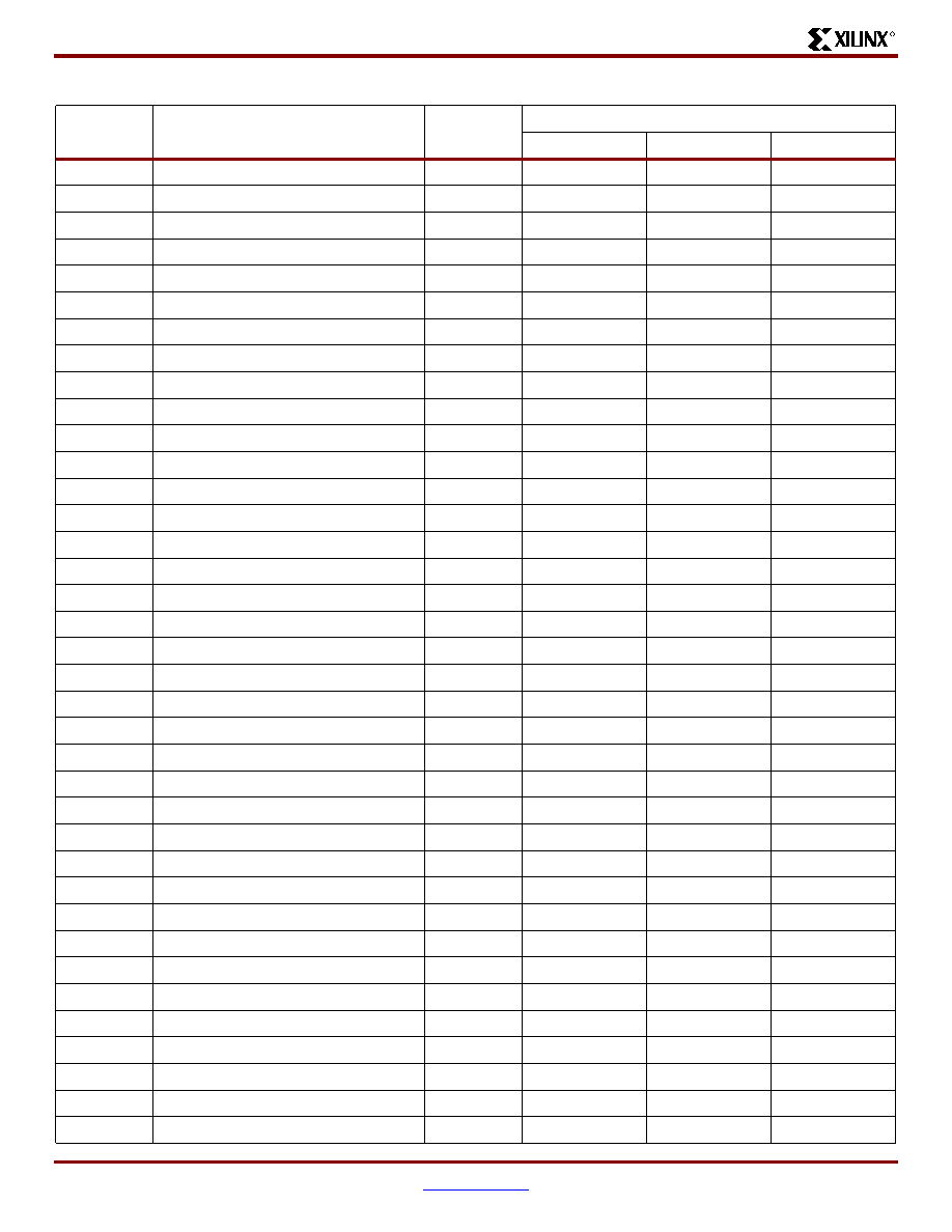
FF672 Flip-Chip Fine-Pitch BGA Package
R
62
www.xilinx.com
DS083-4 (v2.5.5) August 25, 2003
1-800-255-7778
Advance Product Specification
2
VCCO_2
K2
2
VCCO_2
K8
2
VCCO_2
L9
2
VCCO_2
M9
2
VCCO_2
N9
3
VCCO_3
P9
3
VCCO_3
R9
3
VCCO_3
T9
3
VCCO_3
U2
3
VCCO_3
U8
3
VCCO_3
V8
3
VCCO_3
Y2
4
VCCO_4
W9
4
VCCO_4
AD7
4
VCCO_4
V11
4
VCCO_4
V12
4
VCCO_4
V13
4
VCCO_4
W10
4
VCCO_4
AD10
5
VCCO_5
V14
5
VCCO_5
V15
5
VCCO_5
V16
5
VCCO_5
W17
5
VCCO_5
W18
5
VCCO_5
AD17
5
VCCO_5
AD20
6
VCCO_6
P18
6
VCCO_6
R18
6
VCCO_6
T18
6
VCCO_6
U19
6
VCCO_6
U25
6
VCCO_6
V19
6
VCCO_6
Y25
7
VCCO_7
G25
7
VCCO_7
J19
7
VCCO_7
K19
7
VCCO_7
K25
Table 8: FF672 -- XC2VP2, XC2VP4, and XC2VP7
Bank
Pin Description
Pin
Number
No Connects
XC2VP2
XC2VP4
XC2VP7
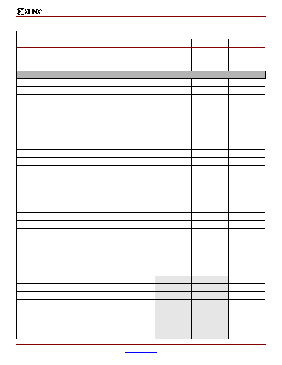
Virtex-II ProTM Platform FPGAs: Pinout Information
R
DS083-4 (v2.5.5) August 25, 2003
www.xilinx.com
63
Advance Product Specification
1-800-255-7778
7
VCCO_7
L18
7
VCCO_7
M18
7
VCCO_7
N18
N/A
CCLK
W7
N/A
PROG_B
D22
N/A
DONE
AB6
N/A
M0
AC22
N/A
M1
W20
N/A
M2
AB21
N/A
TCK
G8
N/A
TDI
H20
N/A
TDO
H7
N/A
TMS
F7
N/A
PWRDWN_B
AC5
N/A
HSWAP_EN
E21
N/A
RSVD
D5
N/A
VBATT
E6
N/A
DXP
F20
N/A
DXN
G19
N/A
AVCCAUXTX7
B11
N/A
VTTXPAD7
B12
N/A
TXNPAD7
A12
N/A
TXPPAD7
A11
N/A
GNDA7
C11
N/A
RXPPAD7
A10
N/A
RXNPAD7
A9
N/A
VTRXPAD7
B10
N/A
AVCCAUXRX7
B9
N/A
AVCCAUXTX9
B6
NC
NC
N/A
VTTXPAD9
B7
NC
NC
N/A
TXNPAD9
A7
NC
NC
N/A
TXPPAD9
A6
NC
NC
N/A
GNDA9
C5
NC
NC
N/A
RXPPAD9
A5
NC
NC
N/A
RXNPAD9
A4
NC
NC
N/A
VTRXPAD9
B5
NC
NC
Table 8: FF672 -- XC2VP2, XC2VP4, and XC2VP7
Bank
Pin Description
Pin
Number
No Connects
XC2VP2
XC2VP4
XC2VP7
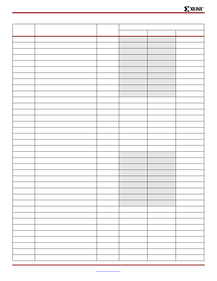
FF672 Flip-Chip Fine-Pitch BGA Package
R
64
www.xilinx.com
DS083-4 (v2.5.5) August 25, 2003
1-800-255-7778
Advance Product Specification
N/A
AVCCAUXRX9
B4
NC
NC
N/A
AVCCAUXRX16
AE4
NC
NC
N/A
VTRXPAD16
AE5
NC
NC
N/A
RXNPAD16
AF4
NC
NC
N/A
RXPPAD16
AF5
NC
NC
N/A
GNDA16
AD5
NC
NC
N/A
TXPPAD16
AF6
NC
NC
N/A
TXNPAD16
AF7
NC
NC
N/A
VTTXPAD16
AE7
NC
NC
N/A
AVCCAUXTX16
AE6
NC
NC
N/A
AVCCAUXRX18
AE9
N/A
VTRXPAD18
AE10
N/A
RXNPAD18
AF9
N/A
RXPPAD18
AF10
N/A
GNDA18
AD11
N/A
TXPPAD18
AF11
N/A
TXNPAD18
AF12
N/A
VTTXPAD18
AE12
N/A
AVCCAUXTX18
AE11
N/A
AVCCAUXTX4
B22
NC
NC
N/A
VTTXPAD4
B23
NC
NC
N/A
TXNPAD4
A23
NC
NC
N/A
TXPPAD4
A22
NC
NC
N/A
GNDA4
C22
NC
NC
N/A
RXPPAD4
A21
NC
NC
N/A
RXNPAD4
A20
NC
NC
N/A
VTRXPAD4
B21
NC
NC
N/A
AVCCAUXRX4
B20
NC
NC
N/A
AVCCAUXTX6
B17
N/A
VTTXPAD6
B18
N/A
TXNPAD6
A18
N/A
TXPPAD6
A17
N/A
GNDA6
C16
N/A
RXPPAD6
A16
N/A
RXNPAD6
A15
N/A
VTRXPAD6
B16
N/A
AVCCAUXRX6
B15
Table 8: FF672 -- XC2VP2, XC2VP4, and XC2VP7
Bank
Pin Description
Pin
Number
No Connects
XC2VP2
XC2VP4
XC2VP7

Virtex-II ProTM Platform FPGAs: Pinout Information
R
DS083-4 (v2.5.5) August 25, 2003
www.xilinx.com
65
Advance Product Specification
1-800-255-7778
N/A
AVCCAUXRX19
AE15
N/A
VTRXPAD19
AE16
N/A
RXNPAD19
AF15
N/A
RXPPAD19
AF16
N/A
GNDA19
AD16
N/A
TXPPAD19
AF17
N/A
TXNPAD19
AF18
N/A
VTTXPAD19
AE18
N/A
AVCCAUXTX19
AE17
N/A
AVCCAUXRX21
AE20
NC
NC
N/A
VTRXPAD21
AE21
NC
NC
N/A
RXNPAD21
AF20
NC
NC
N/A
RXPPAD21
AF21
NC
NC
N/A
GNDA21
AD22
NC
NC
N/A
TXPPAD21
AF22
NC
NC
N/A
TXNPAD21
AF23
NC
NC
N/A
VTTXPAD21
AE23
NC
NC
N/A
AVCCAUXTX21
AE22
NC
NC
N/A
VCCINT
H8
N/A
VCCINT
J9
N/A
VCCINT
K9
N/A
VCCINT
U9
N/A
VCCINT
V9
N/A
VCCINT
W8
N/A
VCCINT
H19
N/A
VCCINT
J10
N/A
VCCINT
J17
N/A
VCCINT
J18
N/A
VCCINT
K11
N/A
VCCINT
K16
N/A
VCCINT
K18
N/A
VCCINT
L10
N/A
VCCINT
L17
N/A
VCCINT
T10
N/A
VCCINT
T17
N/A
VCCINT
U11
Table 8: FF672 -- XC2VP2, XC2VP4, and XC2VP7
Bank
Pin Description
Pin
Number
No Connects
XC2VP2
XC2VP4
XC2VP7

FF672 Flip-Chip Fine-Pitch BGA Package
R
66
www.xilinx.com
DS083-4 (v2.5.5) August 25, 2003
1-800-255-7778
Advance Product Specification
N/A
VCCINT
U16
N/A
VCCINT
U18
N/A
VCCINT
V10
N/A
VCCINT
V17
N/A
VCCINT
V18
N/A
VCCINT
W19
N/A
VCCAUX
B2
N/A
VCCAUX
N1
N/A
VCCAUX
P1
N/A
VCCAUX
A13
N/A
VCCAUX
A14
N/A
VCCAUX
AE2
N/A
VCCAUX
B25
N/A
VCCAUX
N26
N/A
VCCAUX
P26
N/A
VCCAUX
AE25
N/A
VCCAUX
AF13
N/A
VCCAUX
AF14
N/A
GND
C3
N/A
GND
D4
N/A
GND
E5
N/A
GND
F6
N/A
GND
G7
N/A
GND
Y7
N/A
GND
AA6
N/A
GND
AB5
N/A
GND
AC4
N/A
GND
AD3
N/A
GND
C24
N/A
GND
D23
N/A
GND
E22
N/A
GND
F21
N/A
GND
G20
N/A
GND
K10
N/A
GND
K12
N/A
GND
K13
N/A
GND
K14
Table 8: FF672 -- XC2VP2, XC2VP4, and XC2VP7
Bank
Pin Description
Pin
Number
No Connects
XC2VP2
XC2VP4
XC2VP7

Virtex-II ProTM Platform FPGAs: Pinout Information
R
DS083-4 (v2.5.5) August 25, 2003
www.xilinx.com
67
Advance Product Specification
1-800-255-7778
N/A
GND
K15
N/A
GND
K17
N/A
GND
L11
N/A
GND
L12
N/A
GND
L13
N/A
GND
L14
N/A
GND
L15
N/A
GND
L16
N/A
GND
M10
N/A
GND
M11
N/A
GND
M12
N/A
GND
M13
N/A
GND
M14
N/A
GND
M15
N/A
GND
M16
N/A
GND
M17
N/A
GND
N10
N/A
GND
N11
N/A
GND
N12
N/A
GND
N13
N/A
GND
N14
N/A
GND
N15
N/A
GND
N16
N/A
GND
N17
N/A
GND
P10
N/A
GND
P11
N/A
GND
P12
N/A
GND
P13
N/A
GND
P14
N/A
GND
P15
N/A
GND
P16
N/A
GND
P17
N/A
GND
R10
N/A
GND
R11
N/A
GND
R12
N/A
GND
R13
N/A
GND
R14
Table 8: FF672 -- XC2VP2, XC2VP4, and XC2VP7
Bank
Pin Description
Pin
Number
No Connects
XC2VP2
XC2VP4
XC2VP7
FF672 Flip-Chip Fine-Pitch BGA Package
R
68
www.xilinx.com
DS083-4 (v2.5.5) August 25, 2003
1-800-255-7778
Advance Product Specification
N/A
GND
R15
N/A
GND
R16
N/A
GND
R17
N/A
GND
T11
N/A
GND
T12
N/A
GND
T13
N/A
GND
T14
N/A
GND
T15
N/A
GND
T16
N/A
GND
U10
N/A
GND
U12
N/A
GND
U13
N/A
GND
U14
N/A
GND
U15
N/A
GND
U17
N/A
GND
Y20
N/A
GND
AA21
N/A
GND
AB22
N/A
GND
AC23
N/A
GND
AD24
Notes:
1.
See
Table 4
for an explanation of the signals available on this pin.
Table 8: FF672 -- XC2VP2, XC2VP4, and XC2VP7
Bank
Pin Description
Pin
Number
No Connects
XC2VP2
XC2VP4
XC2VP7
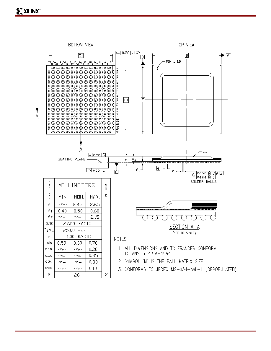
Virtex-II ProTM Platform FPGAs: Pinout Information
R
DS083-4 (v2.5.5) August 25, 2003
www.xilinx.com
69
Advance Product Specification
1-800-255-7778
FF672 Flip-Chip Fine-Pitch BGA Package Specifications (1.00mm pitch)
Figure 4: FF672 Flip-Chip Fine-Pitch BGA Package Specifications
FF896 Flip-Chip Fine-Pitch BGA Package
R
70
www.xilinx.com
DS083-4 (v2.5.5) August 25, 2003
1-800-255-7778
Advance Product Specification
FF896 Flip-Chip Fine-Pitch BGA Package
As shown in
Table 9
, XC2VP7, XC2VP20, and XC2VP30 Virtex-II Pro devices are available in the FF896 flip-chip fine-pitch
BGA package. Pins in each of these devices are the same, except for differences shown in the "No Connects" column.
Following this table are the
FF896 Flip-Chip Fine-Pitch BGA Package Specifications (1.00mm pitch)
.
Table 9: FF896 -- XC2VP7, XC2VP20, and XC2VP30
Bank
Pin Description
Pin Number
No Connects
XC2VP7
XC2VP20
XC2VP30
0
IO_L01N_0/VRP_0
E25
0
IO_L01P_0/VRN_0
E24
0
IO_L02N_0
F24
0
IO_L02P_0
F23
0
IO_L03N_0
E23
0
IO_L03P_0/VREF_0
E22
0
IO_L05_0/No_Pair
G23
0
IO_L06N_0
H22
0
IO_L06P_0
G22
0
IO_L07N_0
F22
0
IO_L07P_0
F21
0
IO_L08N_0
D24
0
IO_L08P_0
C24
0
IO_L09N_0
H21
0
IO_L09P_0/VREF_0
G21
0
IO_L37N_0
E21
0
IO_L37P_0
D21
0
IO_L38N_0
D23
0
IO_L38P_0
C23
0
IO_L39N_0
H20
0
IO_L39P_0
G20
0
IO_L43N_0
E20
0
IO_L43P_0
D20
0
IO_L44N_0
B23
0
IO_L44P_0
A23
0
IO_L45N_0
H19
0
IO_L45P_0/VREF_0
G19
0
IO_L46N_0
E19
NC
0
IO_L46P_0
E18
NC
0
IO_L47N_0
C22
NC
0
IO_L47P_0
B22
NC
0
IO_L48N_0
F20
NC
0
IO_L48P_0
F19
NC
Virtex-II ProTM Platform FPGAs: Pinout Information
R
DS083-4 (v2.5.5) August 25, 2003
www.xilinx.com
71
Advance Product Specification
1-800-255-7778
0
IO_L49N_0
G17
NC
0
IO_L49P_0
F17
NC
0
IO_L50_0/No_Pair
B21
NC
0
IO_L53_0/No_Pair
A21
NC
0
IO_L54N_0
H18
NC
0
IO_L54P_0
G18
NC
0
IO_L56N_0
C21
NC
0
IO_L56P_0
C20
NC
0
IO_L57N_0
J17
NC
0
IO_L57P_0/VREF_0
H17
NC
0
IO_L67N_0
E17
0
IO_L67P_0
D17
0
IO_L68N_0
D18
0
IO_L68P_0
C18
0
IO_L69N_0
J16
0
IO_L69P_0/VREF_0
H16
0
IO_L73N_0
E16
0
IO_L73P_0
D16
0
IO_L74N_0/GCLK7P
C16
0
IO_L74P_0/GCLK6S
B16
0
IO_L75N_0/GCLK5P
G16
0
IO_L75P_0/GCLK4S
F16
1
IO_L75N_1/GCLK3P
F15
1
IO_L75P_1/GCLK2S
G15
1
IO_L74N_1/GCLK1P
B15
1
IO_L74P_1/GCLK0S
C15
1
IO_L73N_1
D15
1
IO_L73P_1
E15
1
IO_L69N_1/VREF_1
H15
1
IO_L69P_1
J15
1
IO_L68N_1
C13
1
IO_L68P_1
D13
1
IO_L67N_1
D14
1
IO_L67P_1
E14
1
IO_L57N_1/VREF_1
H14
NC
1
IO_L57P_1
J14
NC
Table 9: FF896 -- XC2VP7, XC2VP20, and XC2VP30
Bank
Pin Description
Pin Number
No Connects
XC2VP7
XC2VP20
XC2VP30
FF896 Flip-Chip Fine-Pitch BGA Package
R
72
www.xilinx.com
DS083-4 (v2.5.5) August 25, 2003
1-800-255-7778
Advance Product Specification
1
IO_L56N_1
C11
NC
1
IO_L56P_1
C10
NC
1
IO_L54N_1
G13
NC
1
IO_L54P_1
H13
NC
1
IO_L53_1/No_Pair
A10
NC
1
IO_L50_1/No_Pair
B10
NC
1
IO_L49N_1
F14
NC
1
IO_L49P_1
G14
NC
1
IO_L48N_1
F12
NC
1
IO_L48P_1
F11
NC
1
IO_L47N_1
B9
NC
1
IO_L47P_1
C9
NC
1
IO_L46N_1
E13
NC
1
IO_L46P_1
E12
NC
1
IO_L45N_1/VREF_1
G12
1
IO_L45P_1
H12
1
IO_L44N_1
A8
1
IO_L44P_1
B8
1
IO_L43N_1
D11
1
IO_L43P_1
E11
1
IO_L39N_1
G11
1
IO_L39P_1
H11
1
IO_L38N_1
C8
1
IO_L38P_1
D8
1
IO_L37N_1
D10
1
IO_L37P_1
E10
1
IO_L09N_1/VREF_1
G10
1
IO_L09P_1
H10
1
IO_L08N_1
C7
1
IO_L08P_1
D7
1
IO_L07N_1
F10
1
IO_L07P_1
F9
1
IO_L06N_1
G9
1
IO_L06P_1
H9
1
IO_L05_1/No_Pair
G8
1
IO_L03N_1/VREF_1
E9
1
IO_L03P_1
E8
Table 9: FF896 -- XC2VP7, XC2VP20, and XC2VP30
Bank
Pin Description
Pin Number
No Connects
XC2VP7
XC2VP20
XC2VP30
Virtex-II ProTM Platform FPGAs: Pinout Information
R
DS083-4 (v2.5.5) August 25, 2003
www.xilinx.com
73
Advance Product Specification
1-800-255-7778
1
IO_L02N_1
F8
1
IO_L02P_1
F7
1
IO_L01N_1/VRP_1
E7
1
IO_L01P_1/VRN_1
E6
2
IO_L01N_2/VRP_2
A3
2
IO_L01P_2/VRN_2
B3
2
IO_L02N_2
G6
2
IO_L02P_2
G5
2
IO_L03N_2
C5
2
IO_L03P_2
D5
2
IO_L04N_2/VREF_2
C2
2
IO_L04P_2
C1
2
IO_L05N_2
J8
2
IO_L05P_2
J7
2
IO_L06N_2
C4
2
IO_L06P_2
D3
2
IO_L31N_2
D2
NC
2
IO_L31P_2
D1
NC
2
IO_L32N_2
H6
NC
2
IO_L32P_2
H5
NC
2
IO_L33N_2
E4
NC
2
IO_L33P_2
E3
NC
2
IO_L34N_2/VREF_2
E2
NC
2
IO_L34P_2
E1
NC
2
IO_L35N_2
K8
NC
2
IO_L35P_2
K7
NC
2
IO_L36N_2
F4
NC
2
IO_L36P_2
F3
NC
2
IO_L37N_2
F2
NC
2
IO_L37P_2
F1
NC
2
IO_L38N_2
J6
NC
2
IO_L38P_2
J5
NC
2
IO_L39N_2
G4
NC
2
IO_L39P_2
G3
NC
2
IO_L40N_2/VREF_2
G2
NC
2
IO_L40P_2
G1
NC
Table 9: FF896 -- XC2VP7, XC2VP20, and XC2VP30
Bank
Pin Description
Pin Number
No Connects
XC2VP7
XC2VP20
XC2VP30

FF896 Flip-Chip Fine-Pitch BGA Package
R
74
www.xilinx.com
DS083-4 (v2.5.5) August 25, 2003
1-800-255-7778
Advance Product Specification
2
IO_L41N_2
L8
NC
2
IO_L41P_2
L7
NC
2
IO_L42N_2
H4
NC
2
IO_L42P_2
H3
NC
2
IO_L43N_2
H2
2
IO_L43P_2
J2
2
IO_L44N_2
M8
2
IO_L44P_2
M7
2
IO_L45N_2
K6
2
IO_L45P_2
K5
2
IO_L46N_2/VREF_2
J1
2
IO_L46P_2
K1
2
IO_L47N_2
M6
2
IO_L47P_2
M5
2
IO_L48N_2
J4
2
IO_L48P_2
J3
2
IO_L49N_2
K2
2
IO_L49P_2
L2
2
IO_L50N_2
N8
2
IO_L50P_2
N7
2
IO_L51N_2
K4
2
IO_L51P_2
K3
2
IO_L52N_2/VREF_2
L1
2
IO_L52P_2
M1
2
IO_L53N_2
N6
2
IO_L53P_2
N5
2
IO_L54N_2
L5
2
IO_L54P_2
L4
2
IO_L55N_2
M2
2
IO_L55P_2
N2
2
IO_L56N_2
P9
2
IO_L56P_2
R9
2
IO_L57N_2
M4
2
IO_L57P_2
M3
2
IO_L58N_2/VREF_2
N1
2
IO_L58P_2
P1
2
IO_L59N_2
P8
Table 9: FF896 -- XC2VP7, XC2VP20, and XC2VP30
Bank
Pin Description
Pin Number
No Connects
XC2VP7
XC2VP20
XC2VP30

Virtex-II ProTM Platform FPGAs: Pinout Information
R
DS083-4 (v2.5.5) August 25, 2003
www.xilinx.com
75
Advance Product Specification
1-800-255-7778
2
IO_L59P_2
P7
2
IO_L60N_2
N4
2
IO_L60P_2
N3
2
IO_L85N_2
P3
2
IO_L85P_2
P2
2
IO_L86N_2
R8
2
IO_L86P_2
R7
2
IO_L87N_2
P5
2
IO_L87P_2
P4
2
IO_L88N_2/VREF_2
R2
2
IO_L88P_2
T2
2
IO_L89N_2
R6
2
IO_L89P_2
R5
2
IO_L90N_2
R4
2
IO_L90P_2
R3
3
IO_L90N_3
U1
3
IO_L90P_3
V1
3
IO_L89N_3
T5
3
IO_L89P_3
T6
3
IO_L88N_3
T3
3
IO_L88P_3
T4
3
IO_L87N_3/VREF_3
U2
3
IO_L87P_3
U3
3
IO_L86N_3
T7
3
IO_L86P_3
T8
3
IO_L85N_3
U4
3
IO_L85P_3
U5
3
IO_L60N_3
V2
3
IO_L60P_3
W2
3
IO_L59N_3
T9
3
IO_L59P_3
U9
3
IO_L58N_3
V3
3
IO_L58P_3
V4
3
IO_L57N_3/VREF_3
W1
3
IO_L57P_3
Y1
3
IO_L56N_3
U7
Table 9: FF896 -- XC2VP7, XC2VP20, and XC2VP30
Bank
Pin Description
Pin Number
No Connects
XC2VP7
XC2VP20
XC2VP30
FF896 Flip-Chip Fine-Pitch BGA Package
R
76
www.xilinx.com
DS083-4 (v2.5.5) August 25, 2003
1-800-255-7778
Advance Product Specification
3
IO_L56P_3
U8
3
IO_L55N_3
V5
3
IO_L55P_3
V6
3
IO_L54N_3
Y2
3
IO_L54P_3
AA2
3
IO_L53N_3
V7
3
IO_L53P_3
V8
3
IO_L52N_3
W3
3
IO_L52P_3
W4
3
IO_L51N_3/VREF_3
AA1
3
IO_L51P_3
AB1
3
IO_L50N_3
W5
3
IO_L50P_3
W6
3
IO_L49N_3
Y4
3
IO_L49P_3
Y5
3
IO_L48N_3
AA3
3
IO_L48P_3
AA4
3
IO_L47N_3
W7
3
IO_L47P_3
W8
3
IO_L46N_3
AB3
3
IO_L46P_3
AB4
3
IO_L45N_3/VREF_3
AB2
3
IO_L45P_3
AC2
3
IO_L44N_3
AA5
3
IO_L44P_3
AA6
3
IO_L43N_3
AC3
3
IO_L43P_3
AC4
3
IO_L42N_3
AD1
NC
3
IO_L42P_3
AD2
NC
3
IO_L41N_3
Y7
NC
3
IO_L41P_3
Y8
NC
3
IO_L40N_3
AB5
NC
3
IO_L40P_3
AB6
NC
3
IO_L39N_3/VREF_3
AE1
NC
3
IO_L39P_3
AE2
NC
3
IO_L38N_3
AA7
NC
3
IO_L38P_3
AA8
NC
Table 9: FF896 -- XC2VP7, XC2VP20, and XC2VP30
Bank
Pin Description
Pin Number
No Connects
XC2VP7
XC2VP20
XC2VP30

Virtex-II ProTM Platform FPGAs: Pinout Information
R
DS083-4 (v2.5.5) August 25, 2003
www.xilinx.com
77
Advance Product Specification
1-800-255-7778
3
IO_L37N_3
AD3
NC
3
IO_L37P_3
AD4
NC
3
IO_L36N_3
AF1
NC
3
IO_L36P_3
AF2
NC
3
IO_L35N_3
AC5
NC
3
IO_L35P_3
AC6
NC
3
IO_L34N_3
AF3
NC
3
IO_L34P_3
AF4
NC
3
IO_L33N_3/VREF_3
AE3
NC
3
IO_L33P_3
AE4
NC
3
IO_L32N_3
AB7
NC
3
IO_L32P_3
AB8
NC
3
IO_L31N_3
AE5
NC
3
IO_L31P_3
AF6
NC
3
IO_L06N_3
AG1
3
IO_L06P_3
AG2
3
IO_L05N_3
AD5
3
IO_L05P_3
AD6
3
IO_L04N_3
AG3
3
IO_L04P_3
AH4
3
IO_L03N_3/VREF_3
AH1
3
IO_L03P_3
AH2
3
IO_L02N_3
AG5
3
IO_L02P_3
AH5
3
IO_L01N_3/VRP_3
AJ3
3
IO_L01P_3/VRN_3
AK3
4
IO_L01N_4/BUSY/DOUT
(1)
AG6
4
IO_L01P_4/INIT_B
AF7
4
IO_L02N_4/D0/DIN
(1)
AC9
4
IO_L02P_4/D1
AD9
4
IO_L03N_4/D2
AG7
4
IO_L03P_4/D3
AH7
4
IO_L05_4/No_Pair
AD8
4
IO_L06N_4/VRP_4
AG8
4
IO_L06P_4/VRN_4
AH8
4
IO_L07N_4
AC10
Table 9: FF896 -- XC2VP7, XC2VP20, and XC2VP30
Bank
Pin Description
Pin Number
No Connects
XC2VP7
XC2VP20
XC2VP30

FF896 Flip-Chip Fine-Pitch BGA Package
R
78
www.xilinx.com
DS083-4 (v2.5.5) August 25, 2003
1-800-255-7778
Advance Product Specification
4
IO_L07P_4/VREF_4
AD10
4
IO_L08N_4
AE7
4
IO_L08P_4
AE8
4
IO_L09N_4
AJ8
4
IO_L09P_4/VREF_4
AK8
4
IO_L37N_4
AC11
4
IO_L37P_4
AD11
4
IO_L38N_4
AF8
4
IO_L38P_4
AF9
4
IO_L39N_4
AF10
4
IO_L39P_4
AG10
4
IO_L43N_4
AC12
4
IO_L43P_4
AD12
4
IO_L44N_4
AE9
4
IO_L44P_4
AE10
4
IO_L45N_4
AH9
4
IO_L45P_4/VREF_4
AJ9
4
IO_L46N_4
AC13
NC
4
IO_L46P_4
AD13
NC
4
IO_L47N_4
AE11
NC
4
IO_L47P_4
AE12
NC
4
IO_L48N_4
AH10
NC
4
IO_L48P_4
AH11
NC
4
IO_L49N_4
AB14
NC
4
IO_L49P_4
AC14
NC
4
IO_L50_4/No_Pair
AF11
NC
4
IO_L53_4/No_Pair
AG11
NC
4
IO_L54N_4
AJ10
NC
4
IO_L54P_4
AK10
NC
4
IO_L56N_4
AF12
NC
4
IO_L56P_4
AF13
NC
4
IO_L57N_4
AG13
NC
4
IO_L57P_4/VREF_4
AH13
NC
4
IO_L67N_4
AB15
4
IO_L67P_4
AC15
4
IO_L68N_4
AD14
4
IO_L68P_4
AE14
Table 9: FF896 -- XC2VP7, XC2VP20, and XC2VP30
Bank
Pin Description
Pin Number
No Connects
XC2VP7
XC2VP20
XC2VP30
Virtex-II ProTM Platform FPGAs: Pinout Information
R
DS083-4 (v2.5.5) August 25, 2003
www.xilinx.com
79
Advance Product Specification
1-800-255-7778
4
IO_L69N_4
AF14
4
IO_L69P_4/VREF_4
AG14
4
IO_L73N_4
AD15
4
IO_L73P_4
AE15
4
IO_L74N_4/GCLK3S
AF15
4
IO_L74P_4/GCLK2P
AG15
4
IO_L75N_4/GCLK1S
AH15
4
IO_L75P_4/GCLK0P
AJ15
5
IO_L75N_5/GCLK7S
AJ16
5
IO_L75P_5/GCLK6P
AH16
5
IO_L74N_5/GCLK5S
AG16
5
IO_L74P_5/GCLK4P
AF16
5
IO_L73N_5
AE16
5
IO_L73P_5
AD16
5
IO_L69N_5/VREF_5
AG17
5
IO_L69P_5
AF17
5
IO_L68N_5
AE17
5
IO_L68P_5
AD17
5
IO_L67N_5
AC16
5
IO_L67P_5
AB16
5
IO_L57N_5/VREF_5
AH18
NC
5
IO_L57P_5
AG18
NC
5
IO_L56N_5
AF18
NC
5
IO_L56P_5
AF19
NC
5
IO_L54N_5
AK21
NC
5
IO_L54P_5
AJ21
NC
5
IO_L53_5/No_Pair
AG20
NC
5
IO_L50_5/No_Pair
AF20
NC
5
IO_L49N_5
AC17
NC
5
IO_L49P_5
AB17
NC
5
IO_L48N_5
AH20
NC
5
IO_L48P_5
AH21
NC
5
IO_L47N_5
AE19
NC
5
IO_L47P_5
AE20
NC
5
IO_L46N_5
AD18
NC
5
IO_L46P_5
AC18
NC
Table 9: FF896 -- XC2VP7, XC2VP20, and XC2VP30
Bank
Pin Description
Pin Number
No Connects
XC2VP7
XC2VP20
XC2VP30
FF896 Flip-Chip Fine-Pitch BGA Package
R
80
www.xilinx.com
DS083-4 (v2.5.5) August 25, 2003
1-800-255-7778
Advance Product Specification
5
IO_L45N_5/VREF_5
AJ22
5
IO_L45P_5
AH22
5
IO_L44N_5
AE21
5
IO_L44P_5
AE22
5
IO_L43N_5
AD19
5
IO_L43P_5
AC19
5
IO_L39N_5
AG21
5
IO_L39P_5
AF21
5
IO_L38N_5
AF22
5
IO_L38P_5
AF23
5
IO_L37N_5
AD20
5
IO_L37P_5
AC20
5
IO_L09N_5/VREF_5
AK23
5
IO_L09P_5
AJ23
5
IO_L08N_5
AE23
5
IO_L08P_5
AE24
5
IO_L07N_5/VREF_5
AD21
5
IO_L07P_5
AC21
5
IO_L06N_5/VRP_5
AH23
5
IO_L06P_5/VRN_5
AG23
5
IO_L05_5/No_Pair
AD23
5
IO_L03N_5/D4
AH24
5
IO_L03P_5/D5
AG24
5
IO_L02N_5/D6
AD22
5
IO_L02P_5/D7
AC22
5
IO_L01N_5/RDWR_B
AF24
5
IO_L01P_5/CS_B
AG25
6
IO_L01P_6/VRN_6
AK28
6
IO_L01N_6/VRP_6
AJ28
6
IO_L02P_6
AH26
6
IO_L02N_6
AG26
6
IO_L03P_6
AH29
6
IO_L03N_6/VREF_6
AH30
6
IO_L04P_6
AH27
6
IO_L04N_6
AG28
6
IO_L05P_6
AD25
Table 9: FF896 -- XC2VP7, XC2VP20, and XC2VP30
Bank
Pin Description
Pin Number
No Connects
XC2VP7
XC2VP20
XC2VP30

Virtex-II ProTM Platform FPGAs: Pinout Information
R
DS083-4 (v2.5.5) August 25, 2003
www.xilinx.com
81
Advance Product Specification
1-800-255-7778
6
IO_L05N_6
AD26
6
IO_L06P_6
AG29
6
IO_L06N_6
AG30
6
IO_L31P_6
AF25
NC
6
IO_L31N_6
AE26
NC
6
IO_L32P_6
AB23
NC
6
IO_L32N_6
AB24
NC
6
IO_L33P_6
AE27
NC
6
IO_L33N_6/VREF_6
AE28
NC
6
IO_L34P_6
AF27
NC
6
IO_L34N_6
AF28
NC
6
IO_L35P_6
AC25
NC
6
IO_L35N_6
AC26
NC
6
IO_L36P_6
AF29
NC
6
IO_L36N_6
AF30
NC
6
IO_L37P_6
AD27
NC
6
IO_L37N_6
AD28
NC
6
IO_L38P_6
AA23
NC
6
IO_L38N_6
AA24
NC
6
IO_L39P_6
AE29
NC
6
IO_L39N_6/VREF_6
AE30
NC
6
IO_L40P_6
AB25
NC
6
IO_L40N_6
AB26
NC
6
IO_L41P_6
Y23
NC
6
IO_L41N_6
Y24
NC
6
IO_L42P_6
AD29
NC
6
IO_L42N_6
AD30
NC
6
IO_L43P_6
AC27
6
IO_L43N_6
AC28
6
IO_L44P_6
AA25
6
IO_L44N_6
AA26
6
IO_L45P_6
AC29
6
IO_L45N_6/VREF_6
AB29
6
IO_L46P_6
AB27
6
IO_L46N_6
AB28
6
IO_L47P_6
W23
6
IO_L47N_6
W24
Table 9: FF896 -- XC2VP7, XC2VP20, and XC2VP30
Bank
Pin Description
Pin Number
No Connects
XC2VP7
XC2VP20
XC2VP30

FF896 Flip-Chip Fine-Pitch BGA Package
R
82
www.xilinx.com
DS083-4 (v2.5.5) August 25, 2003
1-800-255-7778
Advance Product Specification
6
IO_L48P_6
AA27
6
IO_L48N_6
AA28
6
IO_L49P_6
Y26
6
IO_L49N_6
Y27
6
IO_L50P_6
W25
6
IO_L50N_6
W26
6
IO_L51P_6
AB30
6
IO_L51N_6/VREF_6
AA30
6
IO_L52P_6
W27
6
IO_L52N_6
W28
6
IO_L53P_6
V23
6
IO_L53N_6
V24
6
IO_L54P_6
AA29
6
IO_L54N_6
Y29
6
IO_L55P_6
V25
6
IO_L55N_6
V26
6
IO_L56P_6
U23
6
IO_L56N_6
U24
6
IO_L57P_6
Y30
6
IO_L57N_6/VREF_6
W30
6
IO_L58P_6
V27
6
IO_L58N_6
V28
6
IO_L59P_6
U22
6
IO_L59N_6
T22
6
IO_L60P_6
W29
6
IO_L60N_6
V29
6
IO_L85P_6
U26
6
IO_L85N_6
U27
6
IO_L86P_6
T23
6
IO_L86N_6
T24
6
IO_L87P_6
U28
6
IO_L87N_6/VREF_6
U29
6
IO_L88P_6
T27
6
IO_L88N_6
T28
6
IO_L89P_6
T25
6
IO_L89N_6
T26
6
IO_L90P_6
V30
Table 9: FF896 -- XC2VP7, XC2VP20, and XC2VP30
Bank
Pin Description
Pin Number
No Connects
XC2VP7
XC2VP20
XC2VP30
Virtex-II ProTM Platform FPGAs: Pinout Information
R
DS083-4 (v2.5.5) August 25, 2003
www.xilinx.com
83
Advance Product Specification
1-800-255-7778
6
IO_L90N_6
U30
7
IO_L90P_7
R28
7
IO_L90N_7
R27
7
IO_L89P_7
R26
7
IO_L89N_7
R25
7
IO_L88P_7
T29
7
IO_L88N_7/VREF_7
R29
7
IO_L87P_7
P27
7
IO_L87N_7
P26
7
IO_L86P_7
R24
7
IO_L86N_7
R23
7
IO_L85P_7
P29
7
IO_L85N_7
P28
7
IO_L60P_7
N28
7
IO_L60N_7
N27
7
IO_L59P_7
P24
7
IO_L59N_7
P23
7
IO_L58P_7
P30
7
IO_L58N_7/VREF_7
N30
7
IO_L57P_7
M28
7
IO_L57N_7
M27
7
IO_L56P_7
R22
7
IO_L56N_7
P22
7
IO_L55P_7
N29
7
IO_L55N_7
M29
7
IO_L54P_7
L27
7
IO_L54N_7
L26
7
IO_L53P_7
N26
7
IO_L53N_7
N25
7
IO_L52P_7
M30
7
IO_L52N_7/VREF_7
L30
7
IO_L51P_7
K28
7
IO_L51N_7
K27
7
IO_L50P_7
N24
7
IO_L50N_7
N23
7
IO_L49P_7
L29
Table 9: FF896 -- XC2VP7, XC2VP20, and XC2VP30
Bank
Pin Description
Pin Number
No Connects
XC2VP7
XC2VP20
XC2VP30
FF896 Flip-Chip Fine-Pitch BGA Package
R
84
www.xilinx.com
DS083-4 (v2.5.5) August 25, 2003
1-800-255-7778
Advance Product Specification
7
IO_L49N_7
K29
7
IO_L48P_7
J28
7
IO_L48N_7
J27
7
IO_L47P_7
M26
7
IO_L47N_7
M25
7
IO_L46P_7
K30
7
IO_L46N_7/VREF_7
J30
7
IO_L45P_7
K26
7
IO_L45N_7
K25
7
IO_L44P_7
M24
7
IO_L44N_7
M23
7
IO_L43P_7
J29
7
IO_L43N_7
H29
7
IO_L42P_7
H28
NC
7
IO_L42N_7
H27
NC
7
IO_L41P_7
L24
NC
7
IO_L41N_7
L23
NC
7
IO_L40P_7
G30
NC
7
IO_L40N_7/VREF_7
G29
NC
7
IO_L39P_7
G28
NC
7
IO_L39N_7
G27
NC
7
IO_L38P_7
J26
NC
7
IO_L38N_7
J25
NC
7
IO_L37P_7
F30
NC
7
IO_L37N_7
F29
NC
7
IO_L36P_7
F28
NC
7
IO_L36N_7
F27
NC
7
IO_L35P_7
K24
NC
7
IO_L35N_7
K23
NC
7
IO_L34P_7
E30
NC
7
IO_L34N_7/VREF_7
E29
NC
7
IO_L33P_7
E28
NC
7
IO_L33N_7
E27
NC
7
IO_L32P_7
H26
NC
7
IO_L32N_7
H25
NC
7
IO_L31P_7
D30
NC
7
IO_L31N_7
D29
NC
Table 9: FF896 -- XC2VP7, XC2VP20, and XC2VP30
Bank
Pin Description
Pin Number
No Connects
XC2VP7
XC2VP20
XC2VP30

Virtex-II ProTM Platform FPGAs: Pinout Information
R
DS083-4 (v2.5.5) August 25, 2003
www.xilinx.com
85
Advance Product Specification
1-800-255-7778
7
IO_L06P_7
D28
7
IO_L06N_7
C27
7
IO_L05P_7
J24
7
IO_L05N_7
J23
7
IO_L04P_7
C30
7
IO_L04N_7/VREF_7
C29
7
IO_L03P_7
D26
7
IO_L03N_7
C26
7
IO_L02P_7
G26
7
IO_L02N_7
G25
7
IO_L01P_7/VRN_7
B28
7
IO_L01N_7/VRP_7
A28
0
VCCO_0
K21
0
VCCO_0
K20
0
VCCO_0
K19
0
VCCO_0
K18
0
VCCO_0
K17
0
VCCO_0
K16
0
VCCO_0
J21
0
VCCO_0
J20
0
VCCO_0
J19
0
VCCO_0
J18
1
VCCO_1
K15
1
VCCO_1
K14
1
VCCO_1
K13
1
VCCO_1
K12
1
VCCO_1
K11
1
VCCO_1
K10
1
VCCO_1
J13
1
VCCO_1
J12
1
VCCO_1
J11
1
VCCO_1
J10
2
VCCO_2
R10
2
VCCO_2
P10
2
VCCO_2
N10
2
VCCO_2
N9
Table 9: FF896 -- XC2VP7, XC2VP20, and XC2VP30
Bank
Pin Description
Pin Number
No Connects
XC2VP7
XC2VP20
XC2VP30

FF896 Flip-Chip Fine-Pitch BGA Package
R
86
www.xilinx.com
DS083-4 (v2.5.5) August 25, 2003
1-800-255-7778
Advance Product Specification
2
VCCO_2
M10
2
VCCO_2
M9
2
VCCO_2
L10
2
VCCO_2
L9
2
VCCO_2
K9
2
VCCO_2
J9
3
VCCO_3
AB9
3
VCCO_3
AA9
3
VCCO_3
Y10
3
VCCO_3
Y9
3
VCCO_3
W10
3
VCCO_3
W9
3
VCCO_3
V10
3
VCCO_3
V9
3
VCCO_3
U10
3
VCCO_3
T10
4
VCCO_4
AB13
4
VCCO_4
AB12
4
VCCO_4
AB11
4
VCCO_4
AB10
4
VCCO_4
AA15
4
VCCO_4
AA14
4
VCCO_4
AA13
4
VCCO_4
AA12
4
VCCO_4
AA11
4
VCCO_4
AA10
5
VCCO_5
AB21
5
VCCO_5
AB20
5
VCCO_5
AB19
5
VCCO_5
AB18
5
VCCO_5
AA21
5
VCCO_5
AA20
5
VCCO_5
AA19
5
VCCO_5
AA18
5
VCCO_5
AA17
5
VCCO_5
AA16
6
VCCO_6
AB22
Table 9: FF896 -- XC2VP7, XC2VP20, and XC2VP30
Bank
Pin Description
Pin Number
No Connects
XC2VP7
XC2VP20
XC2VP30
Virtex-II ProTM Platform FPGAs: Pinout Information
R
DS083-4 (v2.5.5) August 25, 2003
www.xilinx.com
87
Advance Product Specification
1-800-255-7778
6
VCCO_6
AA22
6
VCCO_6
Y22
6
VCCO_6
Y21
6
VCCO_6
W22
6
VCCO_6
W21
6
VCCO_6
V22
6
VCCO_6
V21
6
VCCO_6
U21
6
VCCO_6
T21
7
VCCO_7
R21
7
VCCO_7
P21
7
VCCO_7
N22
7
VCCO_7
N21
7
VCCO_7
M22
7
VCCO_7
M21
7
VCCO_7
L22
7
VCCO_7
L21
7
VCCO_7
K22
7
VCCO_7
J22
N/A
CCLK
AC7
N/A
PROG_B
G24
N/A
DONE
AC8
N/A
M0
AD24
N/A
M1
AC24
N/A
M2
AC23
N/A
TCK
G7
N/A
TDI
F26
N/A
TDO
F5
N/A
TMS
H8
N/A
PWRDWN_B
AD7
N/A
HSWAP_EN
H23
N/A
RSVD
D6
N/A
VBATT
H7
N/A
DXP
H24
N/A
DXN
D25
N/A
AVCCAUXTX4
B26
Table 9: FF896 -- XC2VP7, XC2VP20, and XC2VP30
Bank
Pin Description
Pin Number
No Connects
XC2VP7
XC2VP20
XC2VP30
FF896 Flip-Chip Fine-Pitch BGA Package
R
88
www.xilinx.com
DS083-4 (v2.5.5) August 25, 2003
1-800-255-7778
Advance Product Specification
N/A
VTTXPAD4
B27
N/A
TXNPAD4
A27
N/A
TXPPAD4
A26
N/A
GNDA4
C25
N/A
RXPPAD4
A25
N/A
RXNPAD4
A24
N/A
VTRXPAD4
B25
N/A
AVCCAUXRX4
B24
N/A
AVCCAUXTX6
B19
N/A
VTTXPAD6
B20
N/A
TXNPAD6
A20
N/A
TXPPAD6
A19
N/A
GNDA6
C19
N/A
RXPPAD6
A18
N/A
RXNPAD6
A17
N/A
VTRXPAD6
B18
N/A
AVCCAUXRX6
B17
N/A
AVCCAUXTX7
B13
N/A
VTTXPAD7
B14
N/A
TXNPAD7
A14
N/A
TXPPAD7
A13
N/A
GNDA7
C12
N/A
RXPPAD7
A12
N/A
RXNPAD7
A11
N/A
VTRXPAD7
B12
N/A
AVCCAUXRX7
B11
N/A
AVCCAUXTX9
B6
N/A
VTTXPAD9
B7
N/A
TXNPAD9
A7
N/A
TXPPAD9
A6
N/A
GNDA9
C6
N/A
RXPPAD9
A5
N/A
RXNPAD9
A4
N/A
VTRXPAD9
B5
N/A
AVCCAUXRX9
B4
N/A
AVCCAUXRX16
AJ4
N/A
VTRXPAD16
AJ5
Table 9: FF896 -- XC2VP7, XC2VP20, and XC2VP30
Bank
Pin Description
Pin Number
No Connects
XC2VP7
XC2VP20
XC2VP30

Virtex-II ProTM Platform FPGAs: Pinout Information
R
DS083-4 (v2.5.5) August 25, 2003
www.xilinx.com
89
Advance Product Specification
1-800-255-7778
N/A
RXNPAD16
AK4
N/A
RXPPAD16
AK5
N/A
GNDA16
AH6
N/A
TXPPAD16
AK6
N/A
TXNPAD16
AK7
N/A
VTTXPAD16
AJ7
N/A
AVCCAUXTX16
AJ6
N/A
AVCCAUXRX18
AJ11
N/A
VTRXPAD18
AJ12
N/A
RXNPAD18
AK11
N/A
RXPPAD18
AK12
N/A
GNDA18
AH12
N/A
TXPPAD18
AK13
N/A
TXNPAD18
AK14
N/A
VTTXPAD18
AJ14
N/A
AVCCAUXTX18
AJ13
N/A
AVCCAUXRX19
AJ17
N/A
VTRXPAD19
AJ18
N/A
RXNPAD19
AK17
N/A
RXPPAD19
AK18
N/A
GNDA19
AH19
N/A
TXPPAD19
AK19
N/A
TXNPAD19
AK20
N/A
VTTXPAD19
AJ20
N/A
AVCCAUXTX19
AJ19
N/A
AVCCAUXRX21
AJ24
N/A
VTRXPAD21
AJ25
N/A
RXNPAD21
AK24
N/A
RXPPAD21
AK25
N/A
GNDA21
AH25
N/A
TXPPAD21
AK26
N/A
TXNPAD21
AK27
N/A
VTTXPAD21
AJ27
N/A
AVCCAUXTX21
AJ26
N/A
VCCAUX
AK29
N/A
VCCAUX
AK16
Table 9: FF896 -- XC2VP7, XC2VP20, and XC2VP30
Bank
Pin Description
Pin Number
No Connects
XC2VP7
XC2VP20
XC2VP30

FF896 Flip-Chip Fine-Pitch BGA Package
R
90
www.xilinx.com
DS083-4 (v2.5.5) August 25, 2003
1-800-255-7778
Advance Product Specification
N/A
VCCAUX
AK15
N/A
VCCAUX
AK2
N/A
VCCAUX
AJ30
N/A
VCCAUX
AJ1
N/A
VCCAUX
T30
N/A
VCCAUX
T1
N/A
VCCAUX
R30
N/A
VCCAUX
R1
N/A
VCCAUX
B30
N/A
VCCAUX
B1
N/A
VCCAUX
A29
N/A
VCCAUX
A16
N/A
VCCAUX
A15
N/A
VCCAUX
A2
N/A
VCCINT
Y19
N/A
VCCINT
Y18
N/A
VCCINT
Y17
N/A
VCCINT
Y16
N/A
VCCINT
Y15
N/A
VCCINT
Y14
N/A
VCCINT
Y13
N/A
VCCINT
Y12
N/A
VCCINT
W20
N/A
VCCINT
W11
N/A
VCCINT
V20
N/A
VCCINT
V11
N/A
VCCINT
U20
N/A
VCCINT
U11
N/A
VCCINT
T20
N/A
VCCINT
T11
N/A
VCCINT
R20
N/A
VCCINT
R11
N/A
VCCINT
P20
N/A
VCCINT
P11
N/A
VCCINT
N20
N/A
VCCINT
N11
N/A
VCCINT
M20
Table 9: FF896 -- XC2VP7, XC2VP20, and XC2VP30
Bank
Pin Description
Pin Number
No Connects
XC2VP7
XC2VP20
XC2VP30
Virtex-II ProTM Platform FPGAs: Pinout Information
R
DS083-4 (v2.5.5) August 25, 2003
www.xilinx.com
91
Advance Product Specification
1-800-255-7778
N/A
VCCINT
M11
N/A
VCCINT
L19
N/A
VCCINT
L18
N/A
VCCINT
L17
N/A
VCCINT
L16
N/A
VCCINT
L15
N/A
VCCINT
L14
N/A
VCCINT
L13
N/A
VCCINT
L12
N/A
GND
AK22
N/A
GND
AK9
N/A
GND
AJ29
N/A
GND
AJ2
N/A
GND
AH28
N/A
GND
AH17
N/A
GND
AH14
N/A
GND
AH3
N/A
GND
AG27
N/A
GND
AG22
N/A
GND
AG19
N/A
GND
AG12
N/A
GND
AG9
N/A
GND
AG4
N/A
GND
AF26
N/A
GND
AF5
N/A
GND
AE25
N/A
GND
AE18
N/A
GND
AE13
N/A
GND
AE6
N/A
GND
AC30
N/A
GND
AC1
N/A
GND
Y28
N/A
GND
Y25
N/A
GND
Y20
N/A
GND
Y11
N/A
GND
Y6
N/A
GND
Y3
Table 9: FF896 -- XC2VP7, XC2VP20, and XC2VP30
Bank
Pin Description
Pin Number
No Connects
XC2VP7
XC2VP20
XC2VP30

FF896 Flip-Chip Fine-Pitch BGA Package
R
92
www.xilinx.com
DS083-4 (v2.5.5) August 25, 2003
1-800-255-7778
Advance Product Specification
N/A
GND
W19
N/A
GND
W18
N/A
GND
W17
N/A
GND
W16
N/A
GND
W15
N/A
GND
W14
N/A
GND
W13
N/A
GND
W12
N/A
GND
V19
N/A
GND
V18
N/A
GND
V17
N/A
GND
V16
N/A
GND
V15
N/A
GND
V14
N/A
GND
V13
N/A
GND
V12
N/A
GND
U25
N/A
GND
U19
N/A
GND
U18
N/A
GND
U17
N/A
GND
U16
N/A
GND
U15
N/A
GND
U14
N/A
GND
U13
N/A
GND
U12
N/A
GND
U6
N/A
GND
T19
N/A
GND
T18
N/A
GND
T17
N/A
GND
T16
N/A
GND
T15
N/A
GND
T14
N/A
GND
T13
N/A
GND
T12
N/A
GND
R19
N/A
GND
R18
N/A
GND
R17
Table 9: FF896 -- XC2VP7, XC2VP20, and XC2VP30
Bank
Pin Description
Pin Number
No Connects
XC2VP7
XC2VP20
XC2VP30

Virtex-II ProTM Platform FPGAs: Pinout Information
R
DS083-4 (v2.5.5) August 25, 2003
www.xilinx.com
93
Advance Product Specification
1-800-255-7778
N/A
GND
R16
N/A
GND
R15
N/A
GND
R14
N/A
GND
R13
N/A
GND
R12
N/A
GND
P25
N/A
GND
P19
N/A
GND
P18
N/A
GND
P17
N/A
GND
P16
N/A
GND
P15
N/A
GND
P14
N/A
GND
P13
N/A
GND
P12
N/A
GND
P6
N/A
GND
N19
N/A
GND
N18
N/A
GND
N17
N/A
GND
N16
N/A
GND
N15
N/A
GND
N14
N/A
GND
N13
N/A
GND
N12
N/A
GND
M19
N/A
GND
M18
N/A
GND
M17
N/A
GND
M16
N/A
GND
M15
N/A
GND
M14
N/A
GND
M13
N/A
GND
M12
N/A
GND
L28
N/A
GND
L25
N/A
GND
L20
N/A
GND
L11
N/A
GND
L6
N/A
GND
L3
Table 9: FF896 -- XC2VP7, XC2VP20, and XC2VP30
Bank
Pin Description
Pin Number
No Connects
XC2VP7
XC2VP20
XC2VP30
FF896 Flip-Chip Fine-Pitch BGA Package
R
94
www.xilinx.com
DS083-4 (v2.5.5) August 25, 2003
1-800-255-7778
Advance Product Specification
N/A
GND
H30
N/A
GND
H1
N/A
GND
F25
N/A
GND
F18
N/A
GND
F13
N/A
GND
F6
N/A
GND
E26
N/A
GND
E5
N/A
GND
D27
N/A
GND
D22
N/A
GND
D19
N/A
GND
D12
N/A
GND
D9
N/A
GND
D4
N/A
GND
C28
N/A
GND
C17
N/A
GND
C14
N/A
GND
C3
N/A
GND
B29
N/A
GND
B2
N/A
GND
A22
N/A
GND
A9
Notes:
1.
See
Table 4
for an explanation of the signals available on this pin.
Table 9: FF896 -- XC2VP7, XC2VP20, and XC2VP30
Bank
Pin Description
Pin Number
No Connects
XC2VP7
XC2VP20
XC2VP30
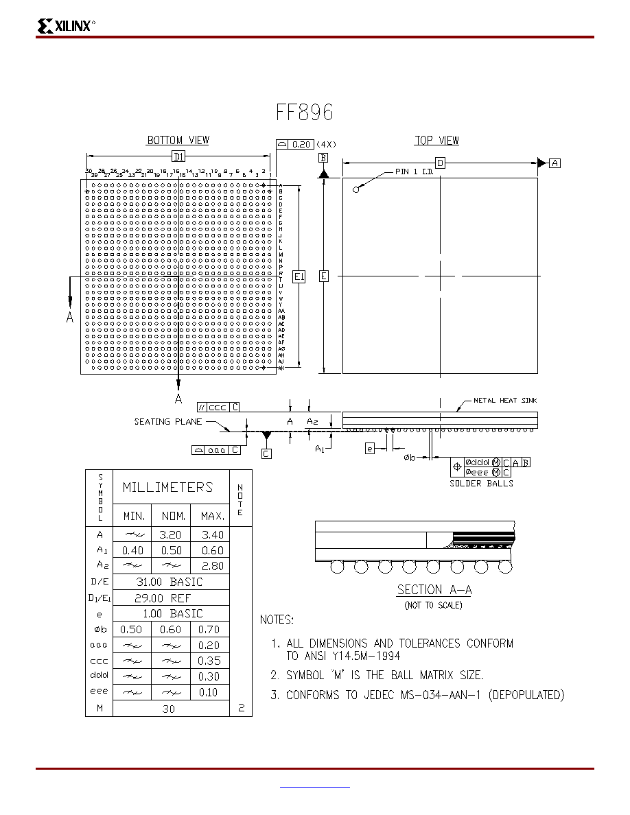
Virtex-II ProTM Platform FPGAs: Pinout Information
R
DS083-4 (v2.5.5) August 25, 2003
www.xilinx.com
95
Advance Product Specification
1-800-255-7778
FF896 Flip-Chip Fine-Pitch BGA Package Specifications (1.00mm pitch)
Figure 5: FF896 Flip-Chip Fine-Pitch BGA Package Specifications

FF1152 Flip-Chip Fine-Pitch BGA Package
R
96
www.xilinx.com
DS083-4 (v2.5.5) August 25, 2003
1-800-255-7778
Advance Product Specification
FF1152 Flip-Chip Fine-Pitch BGA Package
As shown in
Table 10
, XC2VP20, XC2VP30, XC2VP40, and XC2VP50 Virtex-II Pro devices are available in the FF1152
flip-chip fine-pitch BGA package. Pins in each of these devices are the same, except for the differences shown in the No
Connect column. Following this table are the
FF1152 Flip-Chip Fine-Pitch BGA Package Specifications (1.00mm pitch)
.
Table 10: FF1152 -- XC2VP20, XC2VP30, XC2VP40, and XC2VP50
Bank
Pin Description
Pin
Number
No Connects
XC2VP20
XC2VP30
XC2VP40
XC2VP50
0
IO_L01N_0/VRP_0
E29
0
IO_L01P_0/VRN_0
E28
0
IO_L02N_0
H26
0
IO_L02P_0
G26
0
IO_L03N_0
H25
0
IO_L03P_0/VREF_0
G25
0
IO_L05_0/No_Pair
J25
0
IO_L06N_0
K24
0
IO_L06P_0
J24
0
IO_L07N_0
F26
0
IO_L07P_0
E26
0
IO_L08N_0
D30
0
IO_L08P_0
D29
0
IO_L09N_0
K23
0
IO_L09P_0/VREF_0
J23
0
IO_L19N_0
F24
NC
NC
0
IO_L19P_0
E24
NC
NC
0
IO_L20N_0
D28
NC
NC
0
IO_L20P_0
C28
NC
NC
0
IO_L21N_0
H24
NC
NC
0
IO_L21P_0
G24
NC
NC
0
IO_L25N_0
G23
NC
NC
0
IO_L25P_0
F23
NC
NC
0
IO_L26N_0
E27
NC
NC
0
IO_L26P_0
D27
NC
NC
0
IO_L27N_0
K22
NC
NC
0
IO_L27P_0/VREF_0
J22
NC
NC
0
IO_L37N_0
H22
0
IO_L37P_0
G22
0
IO_L38N_0
D26
0
IO_L38P_0
C26
0
IO_L39N_0
K21
0
IO_L39P_0
J21
0
IO_L43N_0
F22

Virtex-II ProTM Platform FPGAs: Pinout Information
R
DS083-4 (v2.5.5) August 25, 2003
www.xilinx.com
97
Advance Product Specification
1-800-255-7778
0
IO_L43P_0
E22
0
IO_L44N_0
E25
0
IO_L44P_0
D25
0
IO_L45N_0
H21
0
IO_L45P_0/VREF_0
G21
0
IO_L46N_0
D22
0
IO_L46P_0
D23
0
IO_L47N_0
D24
0
IO_L47P_0
C24
0
IO_L48N_0
K20
0
IO_L48P_0
J20
0
IO_L49N_0
F21
0
IO_L49P_0
E21
0
IO_L50_0/No_Pair
C21
0
IO_L53_0/No_Pair
C22
0
IO_L54N_0
L19
0
IO_L54P_0
K19
0
IO_L55N_0
G20
0
IO_L55P_0
F20
0
IO_L56N_0
D21
0
IO_L56P_0
D20
0
IO_L57N_0
J19
0
IO_L57P_0/VREF_0
H19
0
IO_L67N_0
G19
0
IO_L67P_0
F19
0
IO_L68N_0
E19
0
IO_L68P_0
D19
0
IO_L69N_0
L18
0
IO_L69P_0/VREF_0
K18
0
IO_L73N_0
G18
0
IO_L73P_0
F18
0
IO_L74N_0/GCLK7P
E18
0
IO_L74P_0/GCLK6S
D18
0
IO_L75N_0/GCLK5P
J18
0
IO_L75P_0/GCLK4S
H18
1
IO_L75N_1/GCLK3P
H17
1
IO_L75P_1/GCLK2S
J17
Table 10: FF1152 -- XC2VP20, XC2VP30, XC2VP40, and XC2VP50
Bank
Pin Description
Pin
Number
No Connects
XC2VP20
XC2VP30
XC2VP40
XC2VP50

FF1152 Flip-Chip Fine-Pitch BGA Package
R
98
www.xilinx.com
DS083-4 (v2.5.5) August 25, 2003
1-800-255-7778
Advance Product Specification
1
IO_L74N_1/GCLK1P
D17
1
IO_L74P_1/GCLK0S
E17
1
IO_L73N_1
F17
1
IO_L73P_1
G17
1
IO_L69N_1/VREF_1
K17
1
IO_L69P_1
L17
1
IO_L68N_1
D16
1
IO_L68P_1
E16
1
IO_L67N_1
F16
1
IO_L67P_1
G16
1
IO_L57N_1/VREF_1
H16
1
IO_L57P_1
J16
1
IO_L56N_1
D15
1
IO_L56P_1
D14
1
IO_L55N_1
F15
1
IO_L55P_1
G15
1
IO_L54N_1
K16
1
IO_L54P_1
L16
1
IO_L53_1/No_Pair
C13
1
IO_L50_1/No_Pair
C14
1
IO_L49N_1
E14
1
IO_L49P_1
F14
1
IO_L48N_1
J15
1
IO_L48P_1
K15
1
IO_L47N_1
C11
1
IO_L47P_1
D11
1
IO_L46N_1
D12
1
IO_L46P_1
D13
1
IO_L45N_1/VREF_1
G14
1
IO_L45P_1
H14
1
IO_L44N_1
D10
1
IO_L44P_1
E10
1
IO_L43N_1
E13
1
IO_L43P_1
F13
1
IO_L39N_1
J14
1
IO_L39P_1
K14
1
IO_L38N_1
C9
1
IO_L38P_1
D9
Table 10: FF1152 -- XC2VP20, XC2VP30, XC2VP40, and XC2VP50
Bank
Pin Description
Pin
Number
No Connects
XC2VP20
XC2VP30
XC2VP40
XC2VP50
Virtex-II ProTM Platform FPGAs: Pinout Information
R
DS083-4 (v2.5.5) August 25, 2003
www.xilinx.com
99
Advance Product Specification
1-800-255-7778
1
IO_L37N_1
G13
1
IO_L37P_1
H13
1
IO_L27N_1/VREF_1
J13
NC
NC
1
IO_L27P_1
K13
NC
NC
1
IO_L26N_1
D8
NC
NC
1
IO_L26P_1
E8
NC
NC
1
IO_L25N_1
F12
NC
NC
1
IO_L25P_1
G12
NC
NC
1
IO_L21N_1
G11
NC
NC
1
IO_L21P_1
H11
NC
NC
1
IO_L20N_1
C7
NC
NC
1
IO_L20P_1
D7
NC
NC
1
IO_L19N_1
E11
NC
NC
1
IO_L19P_1
F11
NC
NC
1
IO_L09N_1/VREF_1
J12
1
IO_L09P_1
K12
1
IO_L08N_1
D6
1
IO_L08P_1
D5
1
IO_L07N_1
E9
1
IO_L07P_1
F9
1
IO_L06N_1
J11
1
IO_L06P_1
K11
1
IO_L05_1/No_Pair
J10
1
IO_L03N_1/VREF_1
G10
1
IO_L03P_1
H10
1
IO_L02N_1
G9
1
IO_L02P_1
H9
1
IO_L01N_1/VRP_1
E7
1
IO_L01P_1/VRN_1
E6
2
IO_L01N_2/VRP_2
D2
2
IO_L01P_2/VRN_2
D1
2
IO_L02N_2
F8
2
IO_L02P_2
F7
2
IO_L03N_2
E4
2
IO_L03P_2
E3
2
IO_L04N_2/VREF_2
E2
2
IO_L04P_2
E1
Table 10: FF1152 -- XC2VP20, XC2VP30, XC2VP40, and XC2VP50
Bank
Pin Description
Pin
Number
No Connects
XC2VP20
XC2VP30
XC2VP40
XC2VP50
FF1152 Flip-Chip Fine-Pitch BGA Package
R
100
www.xilinx.com
DS083-4 (v2.5.5) August 25, 2003
1-800-255-7778
Advance Product Specification
2
IO_L05N_2
J8
2
IO_L05P_2
J7
2
IO_L06N_2
F5
2
IO_L06P_2
F4
2
IO_L15N_2
G4
NC
2
IO_L15P_2
G3
NC
2
IO_L16N_2/VREF_2
G6
NC
2
IO_L16P_2
G5
NC
2
IO_L17N_2
F2
NC
2
IO_L17P_2
F1
NC
2
IO_L18N_2
L10
NC
2
IO_L18P_2
L9
NC
2
IO_L19N_2
H6
NC
2
IO_L19P_2
H5
NC
2
IO_L20N_2
G2
NC
2
IO_L20P_2
G1
NC
2
IO_L21N_2
J6
NC
2
IO_L21P_2
J5
NC
2
IO_L22N_2/VREF_2
J4
NC
2
IO_L22P_2
J3
NC
2
IO_L23N_2
K8
NC
2
IO_L23P_2
K7
NC
2
IO_L24N_2
H4
NC
2
IO_L24P_2
H3
NC
2
IO_L31N_2
H2
2
IO_L31P_2
H1
2
IO_L32N_2
M10
2
IO_L32P_2
M9
2
IO_L33N_2
K5
2
IO_L33P_2
K4
2
IO_L34N_2/VREF_2
J2
2
IO_L34P_2
K2
2
IO_L35N_2
L8
2
IO_L35P_2
L7
2
IO_L36N_2
L6
2
IO_L36P_2
L5
2
IO_L37N_2
K1
2
IO_L37P_2
L1
Table 10: FF1152 -- XC2VP20, XC2VP30, XC2VP40, and XC2VP50
Bank
Pin Description
Pin
Number
No Connects
XC2VP20
XC2VP30
XC2VP40
XC2VP50

Virtex-II ProTM Platform FPGAs: Pinout Information
R
DS083-4 (v2.5.5) August 25, 2003
www.xilinx.com
101
Advance Product Specification
1-800-255-7778
2
IO_L38N_2
N10
2
IO_L38P_2
N9
2
IO_L39N_2
M7
2
IO_L39P_2
M6
2
IO_L40N_2/VREF_2
L2
2
IO_L40P_2
M2
2
IO_L41N_2
N8
2
IO_L41P_2
N7
2
IO_L42N_2
L4
2
IO_L42P_2
L3
2
IO_L43N_2
M4
2
IO_L43P_2
M3
2
IO_L44N_2
P10
2
IO_L44P_2
P9
2
IO_L45N_2
N6
2
IO_L45P_2
N5
2
IO_L46N_2/VREF_2
M1
2
IO_L46P_2
N1
2
IO_L47N_2
P8
2
IO_L47P_2
P7
2
IO_L48N_2
N4
2
IO_L48P_2
N3
2
IO_L49N_2
N2
2
IO_L49P_2
P2
2
IO_L50N_2
R10
2
IO_L50P_2
R9
2
IO_L51N_2
P6
2
IO_L51P_2
P5
2
IO_L52N_2/VREF_2
P4
2
IO_L52P_2
P3
2
IO_L53N_2
T11
2
IO_L53P_2
U11
2
IO_L54N_2
R7
2
IO_L54P_2
R6
2
IO_L55N_2
P1
2
IO_L55P_2
R1
2
IO_L56N_2
T10
2
IO_L56P_2
T9
Table 10: FF1152 -- XC2VP20, XC2VP30, XC2VP40, and XC2VP50
Bank
Pin Description
Pin
Number
No Connects
XC2VP20
XC2VP30
XC2VP40
XC2VP50
FF1152 Flip-Chip Fine-Pitch BGA Package
R
102
www.xilinx.com
DS083-4 (v2.5.5) August 25, 2003
1-800-255-7778
Advance Product Specification
2
IO_L57N_2
R4
2
IO_L57P_2
R3
2
IO_L58N_2/VREF_2
R2
2
IO_L58P_2
T2
2
IO_L59N_2
T8
2
IO_L59P_2
T7
2
IO_L60N_2
T6
2
IO_L60P_2
T5
2
IO_L85N_2
T4
2
IO_L85P_2
T3
2
IO_L86N_2
U10
2
IO_L86P_2
U9
2
IO_L87N_2
U6
2
IO_L87P_2
U5
2
IO_L88N_2/VREF_2
U2
2
IO_L88P_2
V2
2
IO_L89N_2
U8
2
IO_L89P_2
U7
2
IO_L90N_2
U4
2
IO_L90P_2
U3
3
IO_L90N_3
V3
3
IO_L90P_3
V4
3
IO_L89N_3
V7
3
IO_L89P_3
V8
3
IO_L88N_3
V5
3
IO_L88P_3
V6
3
IO_L87N_3/VREF_3
W2
3
IO_L87P_3
Y2
3
IO_L86N_3
V9
3
IO_L86P_3
V10
3
IO_L85N_3
W3
3
IO_L85P_3
W4
3
IO_L60N_3
Y1
3
IO_L60P_3
AA1
3
IO_L59N_3
V11
3
IO_L59P_3
W11
3
IO_L58N_3
W5
Table 10: FF1152 -- XC2VP20, XC2VP30, XC2VP40, and XC2VP50
Bank
Pin Description
Pin
Number
No Connects
XC2VP20
XC2VP30
XC2VP40
XC2VP50
Virtex-II ProTM Platform FPGAs: Pinout Information
R
DS083-4 (v2.5.5) August 25, 2003
www.xilinx.com
103
Advance Product Specification
1-800-255-7778
3
IO_L58P_3
W6
3
IO_L57N_3/VREF_3
Y3
3
IO_L57P_3
Y4
3
IO_L56N_3
W7
3
IO_L56P_3
W8
3
IO_L55N_3
Y6
3
IO_L55P_3
Y7
3
IO_L54N_3
AA2
3
IO_L54P_3
AB2
3
IO_L53N_3
W9
3
IO_L53P_3
W10
3
IO_L52N_3
AA3
3
IO_L52P_3
AA4
3
IO_L51N_3/VREF_3
AB1
3
IO_L51P_3
AC1
3
IO_L50N_3
Y9
3
IO_L50P_3
Y10
3
IO_L49N_3
AA5
3
IO_L49P_3
AA6
3
IO_L48N_3
AB3
3
IO_L48P_3
AB4
3
IO_L47N_3
AA7
3
IO_L47P_3
AA8
3
IO_L46N_3
AB5
3
IO_L46P_3
AB6
3
IO_L45N_3/VREF_3
AC2
3
IO_L45P_3
AD2
3
IO_L44N_3
AA9
3
IO_L44P_3
AA10
3
IO_L43N_3
AC3
3
IO_L43P_3
AC4
3
IO_L42N_3
AD1
3
IO_L42P_3
AE1
3
IO_L41N_3
AB7
3
IO_L41P_3
AB8
3
IO_L40N_3
AC6
3
IO_L40P_3
AC7
3
IO_L39N_3/VREF_3
AD3
Table 10: FF1152 -- XC2VP20, XC2VP30, XC2VP40, and XC2VP50
Bank
Pin Description
Pin
Number
No Connects
XC2VP20
XC2VP30
XC2VP40
XC2VP50

FF1152 Flip-Chip Fine-Pitch BGA Package
R
104
www.xilinx.com
DS083-4 (v2.5.5) August 25, 2003
1-800-255-7778
Advance Product Specification
3
IO_L39P_3
AD4
3
IO_L38N_3
AB9
3
IO_L38P_3
AB10
3
IO_L37N_3
AD5
3
IO_L37P_3
AD6
3
IO_L36N_3
AE2
3
IO_L36P_3
AF2
3
IO_L35N_3
AD7
3
IO_L35P_3
AD8
3
IO_L34N_3
AE4
3
IO_L34P_3
AE5
3
IO_L33N_3/VREF_3
AG1
3
IO_L33P_3
AG2
3
IO_L32N_3
AC9
3
IO_L32P_3
AC10
3
IO_L31N_3
AF3
3
IO_L31P_3
AF4
3
IO_L24N_3
AH1
NC
3
IO_L24P_3
AH2
NC
3
IO_L23N_3
AE7
NC
3
IO_L23P_3
AE8
NC
3
IO_L22N_3
AF5
NC
3
IO_L22P_3
AF6
NC
3
IO_L21N_3/VREF_3
AG3
NC
3
IO_L21P_3
AG4
NC
3
IO_L20N_3
AD9
NC
3
IO_L20P_3
AD10
NC
3
IO_L19N_3
AH3
NC
3
IO_L19P_3
AH4
NC
3
IO_L18N_3
AJ1
NC
3
IO_L18P_3
AJ2
NC
3
IO_L17N_3
AF7
NC
3
IO_L17P_3
AF8
NC
3
IO_L16N_3
AK1
NC
3
IO_L16P_3
AK2
NC
3
IO_L15N_3/VREF_3
AG5
NC
3
IO_L15P_3
AG6
NC
3
IO_L06N_3
AL1
Table 10: FF1152 -- XC2VP20, XC2VP30, XC2VP40, and XC2VP50
Bank
Pin Description
Pin
Number
No Connects
XC2VP20
XC2VP30
XC2VP40
XC2VP50

Virtex-II ProTM Platform FPGAs: Pinout Information
R
DS083-4 (v2.5.5) August 25, 2003
www.xilinx.com
105
Advance Product Specification
1-800-255-7778
3
IO_L06P_3
AL2
3
IO_L05N_3
AG7
3
IO_L05P_3
AH8
3
IO_L04N_3
AH5
3
IO_L04P_3
AH6
3
IO_L03N_3/VREF_3
AK3
3
IO_L03P_3
AK4
3
IO_L02N_3
AJ7
3
IO_L02P_3
AJ8
3
IO_L01N_3/VRP_3
AJ4
3
IO_L01P_3/VRN_3
AJ5
4
IO_L01N_4/BUSY/DOUT
(1)
AL5
4
IO_L01P_4/INIT_B
AL6
4
IO_L02N_4/D0/DIN
(1)
AG9
4
IO_L02P_4/D1
AH9
4
IO_L03N_4/D2
AK6
4
IO_L03P_4/D3
AK7
4
IO_L05_4/No_Pair
AF10
4
IO_L06N_4/VRP_4
AL7
4
IO_L06P_4/VRN_4
AM7
4
IO_L07N_4
AE11
4
IO_L07P_4/VREF_4
AF11
4
IO_L08N_4
AG10
4
IO_L08P_4
AH10
4
IO_L09N_4
AK8
4
IO_L09P_4/VREF_4
AL8
4
IO_L19N_4
AE12
NC
NC
4
IO_L19P_4
AF12
NC
NC
4
IO_L20N_4
AJ9
NC
NC
4
IO_L20P_4
AK9
NC
NC
4
IO_L21N_4
AL9
NC
NC
4
IO_L21P_4
AM9
NC
NC
4
IO_L25N_4
AG11
NC
NC
4
IO_L25P_4
AH11
NC
NC
4
IO_L26N_4
AH12
NC
NC
4
IO_L26P_4
AJ12
NC
NC
4
IO_L27N_4
AK10
NC
NC
Table 10: FF1152 -- XC2VP20, XC2VP30, XC2VP40, and XC2VP50
Bank
Pin Description
Pin
Number
No Connects
XC2VP20
XC2VP30
XC2VP40
XC2VP50
FF1152 Flip-Chip Fine-Pitch BGA Package
R
106
www.xilinx.com
DS083-4 (v2.5.5) August 25, 2003
1-800-255-7778
Advance Product Specification
4
IO_L27P_4/VREF_4
AL10
NC
NC
4
IO_L37N_4
AE13
4
IO_L37P_4
AF13
4
IO_L38N_4
AG13
4
IO_L38P_4
AH13
4
IO_L39N_4
AJ11
4
IO_L39P_4
AK11
4
IO_L43N_4
AE14
4
IO_L43P_4
AF14
4
IO_L44N_4
AJ13
4
IO_L44P_4
AK13
4
IO_L45N_4
AL11
4
IO_L45P_4/VREF_4
AM11
4
IO_L46N_4
AE15
4
IO_L46P_4
AF15
4
IO_L47N_4
AG14
4
IO_L47P_4
AH14
4
IO_L48N_4
AL13
4
IO_L48P_4
AL12
4
IO_L49N_4
AD16
4
IO_L49P_4
AE16
4
IO_L50_4/No_Pair
AJ14
4
IO_L53_4/No_Pair
AK14
4
IO_L54N_4
AM14
4
IO_L54P_4
AM13
4
IO_L55N_4
AF16
4
IO_L55P_4
AG16
4
IO_L56N_4
AH15
4
IO_L56P_4
AJ15
4
IO_L57N_4
AL14
4
IO_L57P_4/VREF_4
AL15
4
IO_L67N_4
AD17
4
IO_L67P_4
AE17
4
IO_L68N_4
AH16
4
IO_L68P_4
AJ16
4
IO_L69N_4
AK16
4
IO_L69P_4/VREF_4
AL16
4
IO_L73N_4
AF17
Table 10: FF1152 -- XC2VP20, XC2VP30, XC2VP40, and XC2VP50
Bank
Pin Description
Pin
Number
No Connects
XC2VP20
XC2VP30
XC2VP40
XC2VP50

Virtex-II ProTM Platform FPGAs: Pinout Information
R
DS083-4 (v2.5.5) August 25, 2003
www.xilinx.com
107
Advance Product Specification
1-800-255-7778
4
IO_L73P_4
AG17
4
IO_L74N_4/GCLK3S
AH17
4
IO_L74P_4/GCLK2P
AJ17
4
IO_L75N_4/GCLK1S
AK17
4
IO_L75P_4/GCLK0P
AL17
5
IO_L75N_5/GCLK7S
AL18
5
IO_L75P_5/GCLK6P
AK18
5
IO_L74N_5/GCLK5S
AJ18
5
IO_L74P_5/GCLK4P
AH18
5
IO_L73N_5
AG18
5
IO_L73P_5
AF18
5
IO_L69N_5/VREF_5
AL19
5
IO_L69P_5
AK19
5
IO_L68N_5
AJ19
5
IO_L68P_5
AH19
5
IO_L67N_5
AE18
5
IO_L67P_5
AD18
5
IO_L57N_5/VREF_5
AL20
5
IO_L57P_5
AL21
5
IO_L56N_5
AJ20
5
IO_L56P_5
AH20
5
IO_L55N_5
AG19
5
IO_L55P_5
AF19
5
IO_L54N_5
AM22
5
IO_L54P_5
AM21
5
IO_L53_5/No_Pair
AK21
5
IO_L50_5/No_Pair
AJ21
5
IO_L49N_5
AE19
5
IO_L49P_5
AD19
5
IO_L48N_5
AL23
5
IO_L48P_5
AL22
5
IO_L47N_5
AH21
5
IO_L47P_5
AG21
5
IO_L46N_5
AF20
5
IO_L46P_5
AE20
5
IO_L45N_5/VREF_5
AM24
5
IO_L45P_5
AL24
Table 10: FF1152 -- XC2VP20, XC2VP30, XC2VP40, and XC2VP50
Bank
Pin Description
Pin
Number
No Connects
XC2VP20
XC2VP30
XC2VP40
XC2VP50
FF1152 Flip-Chip Fine-Pitch BGA Package
R
108
www.xilinx.com
DS083-4 (v2.5.5) August 25, 2003
1-800-255-7778
Advance Product Specification
5
IO_L44N_5
AK22
5
IO_L44P_5
AJ22
5
IO_L43N_5
AF21
5
IO_L43P_5
AE21
5
IO_L39N_5
AK24
5
IO_L39P_5
AJ24
5
IO_L38N_5
AH22
5
IO_L38P_5
AG22
5
IO_L37N_5
AF22
5
IO_L37P_5
AE22
5
IO_L27N_5/VREF_5
AL25
NC
NC
5
IO_L27P_5
AK25
NC
NC
5
IO_L26N_5
AJ23
NC
NC
5
IO_L26P_5
AH23
NC
NC
5
IO_L25N_5
AH24
NC
NC
5
IO_L25P_5
AG24
NC
NC
5
IO_L21N_5
AM26
NC
NC
5
IO_L21P_5
AL26
NC
NC
5
IO_L20N_5
AK26
NC
NC
5
IO_L20P_5
AJ26
NC
NC
5
IO_L19N_5
AF23
NC
NC
5
IO_L19P_5
AE23
NC
NC
5
IO_L09N_5/VREF_5
AL27
5
IO_L09P_5
AK27
5
IO_L08N_5
AH25
5
IO_L08P_5
AG25
5
IO_L07N_5/VREF_5
AF24
5
IO_L07P_5
AE24
5
IO_L06N_5/VRP_5
AM28
5
IO_L06P_5/VRN_5
AL28
5
IO_L05_5/No_Pair
AF25
5
IO_L03N_5/D4
AK28
5
IO_L03P_5/D5
AK29
5
IO_L02N_5/D6
AH26
5
IO_L02P_5/D7
AG26
5
IO_L01N_5/RDWR_B
AL29
5
IO_L01P_5/CS_B
AL30
Table 10: FF1152 -- XC2VP20, XC2VP30, XC2VP40, and XC2VP50
Bank
Pin Description
Pin
Number
No Connects
XC2VP20
XC2VP30
XC2VP40
XC2VP50
Virtex-II ProTM Platform FPGAs: Pinout Information
R
DS083-4 (v2.5.5) August 25, 2003
www.xilinx.com
109
Advance Product Specification
1-800-255-7778
6
IO_L01P_6/VRN_6
AJ30
6
IO_L01N_6/VRP_6
AJ31
6
IO_L02P_6
AJ27
6
IO_L02N_6
AJ28
6
IO_L03P_6
AK31
6
IO_L03N_6/VREF_6
AK32
6
IO_L04P_6
AH29
6
IO_L04N_6
AH30
6
IO_L05P_6
AH27
6
IO_L05N_6
AG28
6
IO_L06P_6
AL33
6
IO_L06N_6
AL34
6
IO_L15P_6
AG29
NC
6
IO_L15N_6/VREF_6
AG30
NC
6
IO_L16P_6
AK33
NC
6
IO_L16N_6
AK34
NC
6
IO_L17P_6
AF27
NC
6
IO_L17N_6
AF28
NC
6
IO_L18P_6
AJ33
NC
6
IO_L18N_6
AJ34
NC
6
IO_L19P_6
AH31
NC
6
IO_L19N_6
AH32
NC
6
IO_L20P_6
AD25
NC
6
IO_L20N_6
AD26
NC
6
IO_L21P_6
AG31
NC
6
IO_L21N_6/VREF_6
AG32
NC
6
IO_L22P_6
AF29
NC
6
IO_L22N_6
AF30
NC
6
IO_L23P_6
AE27
NC
6
IO_L23N_6
AE28
NC
6
IO_L24P_6
AH33
NC
6
IO_L24N_6
AH34
NC
6
IO_L31P_6
AF31
6
IO_L31N_6
AF32
6
IO_L32P_6
AC25
6
IO_L32N_6
AC26
6
IO_L33P_6
AG33
6
IO_L33N_6/VREF_6
AG34
Table 10: FF1152 -- XC2VP20, XC2VP30, XC2VP40, and XC2VP50
Bank
Pin Description
Pin
Number
No Connects
XC2VP20
XC2VP30
XC2VP40
XC2VP50

FF1152 Flip-Chip Fine-Pitch BGA Package
R
110
www.xilinx.com
DS083-4 (v2.5.5) August 25, 2003
1-800-255-7778
Advance Product Specification
6
IO_L34P_6
AE30
6
IO_L34N_6
AE31
6
IO_L35P_6
AD27
6
IO_L35N_6
AD28
6
IO_L36P_6
AF33
6
IO_L36N_6
AE33
6
IO_L37P_6
AD29
6
IO_L37N_6
AD30
6
IO_L38P_6
AB25
6
IO_L38N_6
AB26
6
IO_L39P_6
AD31
6
IO_L39N_6/VREF_6
AD32
6
IO_L40P_6
AC28
6
IO_L40N_6
AC29
6
IO_L41P_6
AB27
6
IO_L41N_6
AB28
6
IO_L42P_6
AE34
6
IO_L42N_6
AD34
6
IO_L43P_6
AC31
6
IO_L43N_6
AC32
6
IO_L44P_6
AA25
6
IO_L44N_6
AA26
6
IO_L45P_6
AD33
6
IO_L45N_6/VREF_6
AC33
6
IO_L46P_6
AB29
6
IO_L46N_6
AB30
6
IO_L47P_6
AA27
6
IO_L47N_6
AA28
6
IO_L48P_6
AB31
6
IO_L48N_6
AB32
6
IO_L49P_6
AA29
6
IO_L49N_6
AA30
6
IO_L50P_6
Y25
6
IO_L50N_6
Y26
6
IO_L51P_6
AC34
6
IO_L51N_6/VREF_6
AB34
6
IO_L52P_6
AA31
6
IO_L52N_6
AA32
Table 10: FF1152 -- XC2VP20, XC2VP30, XC2VP40, and XC2VP50
Bank
Pin Description
Pin
Number
No Connects
XC2VP20
XC2VP30
XC2VP40
XC2VP50

Virtex-II ProTM Platform FPGAs: Pinout Information
R
DS083-4 (v2.5.5) August 25, 2003
www.xilinx.com
111
Advance Product Specification
1-800-255-7778
6
IO_L53P_6
W25
6
IO_L53N_6
W26
6
IO_L54P_6
AB33
6
IO_L54N_6
AA33
6
IO_L55P_6
Y28
6
IO_L55N_6
Y29
6
IO_L56P_6
W27
6
IO_L56N_6
W28
6
IO_L57P_6
Y31
6
IO_L57N_6/VREF_6
Y32
6
IO_L58P_6
W29
6
IO_L58N_6
W30
6
IO_L59P_6
W24
6
IO_L59N_6
V24
6
IO_L60P_6
AA34
6
IO_L60N_6
Y34
6
IO_L85P_6
W31
6
IO_L85N_6
W32
6
IO_L86P_6
V25
6
IO_L86N_6
V26
6
IO_L87P_6
Y33
6
IO_L87N_6/VREF_6
W33
6
IO_L88P_6
V29
6
IO_L88N_6
V30
6
IO_L89P_6
V27
6
IO_L89N_6
V28
6
IO_L90P_6
V31
6
IO_L90N_6
V32
7
IO_L90P_7
U32
7
IO_L90N_7
U31
7
IO_L89P_7
U28
7
IO_L89N_7
U27
7
IO_L88P_7
V33
7
IO_L88N_7/VREF_7
U33
7
IO_L87P_7
U30
7
IO_L87N_7
U29
7
IO_L86P_7
U26
Table 10: FF1152 -- XC2VP20, XC2VP30, XC2VP40, and XC2VP50
Bank
Pin Description
Pin
Number
No Connects
XC2VP20
XC2VP30
XC2VP40
XC2VP50
FF1152 Flip-Chip Fine-Pitch BGA Package
R
112
www.xilinx.com
DS083-4 (v2.5.5) August 25, 2003
1-800-255-7778
Advance Product Specification
7
IO_L86N_7
U25
7
IO_L85P_7
T32
7
IO_L85N_7
T31
7
IO_L60P_7
T30
7
IO_L60N_7
T29
7
IO_L59P_7
T28
7
IO_L59N_7
T27
7
IO_L58P_7
T33
7
IO_L58N_7/VREF_7
R33
7
IO_L57P_7
R32
7
IO_L57N_7
R31
7
IO_L56P_7
T26
7
IO_L56N_7
T25
7
IO_L55P_7
R34
7
IO_L55N_7
P34
7
IO_L54P_7
R29
7
IO_L54N_7
R28
7
IO_L53P_7
U24
7
IO_L53N_7
T24
7
IO_L52P_7
P32
7
IO_L52N_7/VREF_7
P31
7
IO_L51P_7
P30
7
IO_L51N_7
P29
7
IO_L50P_7
R26
7
IO_L50N_7
R25
7
IO_L49P_7
P33
7
IO_L49N_7
N33
7
IO_L48P_7
N32
7
IO_L48N_7
N31
7
IO_L47P_7
P28
7
IO_L47N_7
P27
7
IO_L46P_7
N34
7
IO_L46N_7/VREF_7
M34
7
IO_L45P_7
N30
7
IO_L45N_7
N29
7
IO_L44P_7
P26
7
IO_L44N_7
P25
7
IO_L43P_7
M32
Table 10: FF1152 -- XC2VP20, XC2VP30, XC2VP40, and XC2VP50
Bank
Pin Description
Pin
Number
No Connects
XC2VP20
XC2VP30
XC2VP40
XC2VP50
Virtex-II ProTM Platform FPGAs: Pinout Information
R
DS083-4 (v2.5.5) August 25, 2003
www.xilinx.com
113
Advance Product Specification
1-800-255-7778
7
IO_L43N_7
M31
7
IO_L42P_7
L32
7
IO_L42N_7
L31
7
IO_L41P_7
N28
7
IO_L41N_7
N27
7
IO_L40P_7
M33
7
IO_L40N_7/VREF_7
L33
7
IO_L39P_7
M29
7
IO_L39N_7
M28
7
IO_L38P_7
N26
7
IO_L38N_7
N25
7
IO_L37P_7
L34
7
IO_L37N_7
K34
7
IO_L36P_7
L30
7
IO_L36N_7
L29
7
IO_L35P_7
L28
7
IO_L35N_7
L27
7
IO_L34P_7
K33
7
IO_L34N_7/VREF_7
J33
7
IO_L33P_7
K31
7
IO_L33N_7
K30
7
IO_L32P_7
M26
7
IO_L32N_7
M25
7
IO_L31P_7
H34
7
IO_L31N_7
H33
7
IO_L24P_7
H32
NC
7
IO_L24N_7
H31
NC
7
IO_L23P_7
K28
NC
7
IO_L23N_7
K27
NC
7
IO_L22P_7
J32
NC
7
IO_L22N_7/VREF_7
J31
NC
7
IO_L21P_7
J30
NC
7
IO_L21N_7
J29
NC
7
IO_L20P_7
G34
NC
7
IO_L20N_7
G33
NC
7
IO_L19P_7
H30
NC
7
IO_L19N_7
H29
NC
7
IO_L18P_7
L26
NC
Table 10: FF1152 -- XC2VP20, XC2VP30, XC2VP40, and XC2VP50
Bank
Pin Description
Pin
Number
No Connects
XC2VP20
XC2VP30
XC2VP40
XC2VP50

FF1152 Flip-Chip Fine-Pitch BGA Package
R
114
www.xilinx.com
DS083-4 (v2.5.5) August 25, 2003
1-800-255-7778
Advance Product Specification
7
IO_L18N_7
L25
NC
7
IO_L17P_7
F34
NC
7
IO_L17N_7
F33
NC
7
IO_L16P_7
G30
NC
7
IO_L16N_7/VREF_7
G29
NC
7
IO_L15P_7
G32
NC
7
IO_L15N_7
G31
NC
7
IO_L06P_7
F31
7
IO_L06N_7
F30
7
IO_L05P_7
J28
7
IO_L05N_7
J27
7
IO_L04P_7
E34
7
IO_L04N_7/VREF_7
E33
7
IO_L03P_7
E32
7
IO_L03N_7
E31
7
IO_L02P_7
F28
7
IO_L02N_7
F27
7
IO_L01P_7/VRN_7
D34
7
IO_L01N_7/VRP_7
D33
0
VCCO_0
C29
0
VCCO_0
E20
0
VCCO_0
F25
0
VCCO_0
L20
0
VCCO_0
L21
0
VCCO_0
L22
0
VCCO_0
L23
0
VCCO_0
M18
0
VCCO_0
M19
0
VCCO_0
M20
0
VCCO_0
M21
0
VCCO_0
M22
1
VCCO_1
C6
1
VCCO_1
E15
1
VCCO_1
F10
1
VCCO_1
L12
1
VCCO_1
L13
1
VCCO_1
L14
Table 10: FF1152 -- XC2VP20, XC2VP30, XC2VP40, and XC2VP50
Bank
Pin Description
Pin
Number
No Connects
XC2VP20
XC2VP30
XC2VP40
XC2VP50

Virtex-II ProTM Platform FPGAs: Pinout Information
R
DS083-4 (v2.5.5) August 25, 2003
www.xilinx.com
115
Advance Product Specification
1-800-255-7778
1
VCCO_1
L15
1
VCCO_1
M13
1
VCCO_1
M14
1
VCCO_1
M15
1
VCCO_1
M16
1
VCCO_1
M17
2
VCCO_2
F3
2
VCCO_2
K6
2
VCCO_2
M11
2
VCCO_2
N11
2
VCCO_2
N12
2
VCCO_2
P11
2
VCCO_2
P12
2
VCCO_2
R5
2
VCCO_2
R11
2
VCCO_2
R12
2
VCCO_2
T12
2
VCCO_2
U12
3
VCCO_3
V12
3
VCCO_3
W12
3
VCCO_3
Y5
3
VCCO_3
Y11
3
VCCO_3
Y12
3
VCCO_3
AA11
3
VCCO_3
AA12
3
VCCO_3
AB11
3
VCCO_3
AB12
3
VCCO_3
AC11
3
VCCO_3
AE6
3
VCCO_3
AJ3
4
VCCO_4
AC13
4
VCCO_4
AC14
4
VCCO_4
AC15
4
VCCO_4
AC16
4
VCCO_4
AC17
4
VCCO_4
AD12
4
VCCO_4
AD13
4
VCCO_4
AD14
Table 10: FF1152 -- XC2VP20, XC2VP30, XC2VP40, and XC2VP50
Bank
Pin Description
Pin
Number
No Connects
XC2VP20
XC2VP30
XC2VP40
XC2VP50

FF1152 Flip-Chip Fine-Pitch BGA Package
R
116
www.xilinx.com
DS083-4 (v2.5.5) August 25, 2003
1-800-255-7778
Advance Product Specification
4
VCCO_4
AD15
4
VCCO_4
AJ10
4
VCCO_4
AK15
4
VCCO_4
AM6
5
VCCO_5
AC18
5
VCCO_5
AC19
5
VCCO_5
AC20
5
VCCO_5
AC21
5
VCCO_5
AC22
5
VCCO_5
AD20
5
VCCO_5
AD21
5
VCCO_5
AD22
5
VCCO_5
AD23
5
VCCO_5
AJ25
5
VCCO_5
AK20
5
VCCO_5
AM29
6
VCCO_6
V23
6
VCCO_6
W23
6
VCCO_6
Y23
6
VCCO_6
Y24
6
VCCO_6
Y30
6
VCCO_6
AA23
6
VCCO_6
AA24
6
VCCO_6
AB23
6
VCCO_6
AB24
6
VCCO_6
AC24
6
VCCO_6
AE29
6
VCCO_6
AJ32
7
VCCO_7
F32
7
VCCO_7
K29
7
VCCO_7
M24
7
VCCO_7
N23
7
VCCO_7
N24
7
VCCO_7
P23
7
VCCO_7
P24
7
VCCO_7
R23
7
VCCO_7
R24
7
VCCO_7
R30
Table 10: FF1152 -- XC2VP20, XC2VP30, XC2VP40, and XC2VP50
Bank
Pin Description
Pin
Number
No Connects
XC2VP20
XC2VP30
XC2VP40
XC2VP50

Virtex-II ProTM Platform FPGAs: Pinout Information
R
DS083-4 (v2.5.5) August 25, 2003
www.xilinx.com
117
Advance Product Specification
1-800-255-7778
7
VCCO_7
T23
7
VCCO_7
U23
N/A
CCLK
AE9
N/A
PROG_B
J26
N/A
DONE
AE10
N/A
M0
AF26
N/A
M1
AE26
N/A
M2
AE25
N/A
TCK
J9
N/A
TDI
H28
N/A
TDO
H7
N/A
TMS
K10
N/A
PWRDWN_B
AF9
N/A
HSWAP_EN
K25
N/A
RSVD
G8
N/A
VBATT
K9
N/A
DXP
K26
N/A
DXN
G27
N/A
AVCCAUXTX2
B32
NC
NC
N/A
VTTXPAD2
B33
NC
NC
N/A
TXNPAD2
A33
NC
NC
N/A
TXPPAD2
A32
NC
NC
N/A
GNDA2
C30
NC
NC
N/A
RXPPAD2
A31
NC
NC
N/A
RXNPAD2
A30
NC
NC
N/A
VTRXPAD2
B31
NC
NC
N/A
AVCCAUXRX2
B30
NC
NC
N/A
AVCCAUXTX4
B28
N/A
VTTXPAD4
B29
N/A
TXNPAD4
A29
N/A
TXPPAD4
A28
N/A
GNDA4
C27
N/A
RXPPAD4
A27
N/A
RXNPAD4
A26
N/A
VTRXPAD4
B27
N/A
AVCCAUXRX4
B26
N/A
AVCCAUXTX5
B24
NC
NC
NC
Table 10: FF1152 -- XC2VP20, XC2VP30, XC2VP40, and XC2VP50
Bank
Pin Description
Pin
Number
No Connects
XC2VP20
XC2VP30
XC2VP40
XC2VP50
FF1152 Flip-Chip Fine-Pitch BGA Package
R
118
www.xilinx.com
DS083-4 (v2.5.5) August 25, 2003
1-800-255-7778
Advance Product Specification
N/A
VTTXPAD5
B25
NC
NC
NC
N/A
TXNPAD5
A25
NC
NC
NC
N/A
TXPPAD5
A24
NC
NC
NC
N/A
GNDA5
C23
NC
NC
NC
N/A
RXPPAD5
A23
NC
NC
NC
N/A
RXNPAD5
A22
NC
NC
NC
N/A
VTRXPAD5
B23
NC
NC
NC
N/A
AVCCAUXRX5
B22
NC
NC
NC
N/A
AVCCAUXTX6
B20
N/A
VTTXPAD6
B21
N/A
TXNPAD6
A21
N/A
TXPPAD6
A20
N/A
GNDA6
C20
N/A
RXPPAD6
A19
N/A
RXNPAD6
A18
N/A
VTRXPAD6
B19
N/A
AVCCAUXRX6
B18
N/A
AVCCAUXTX7
B16
N/A
VTTXPAD7
B17
N/A
TXNPAD7
A17
N/A
TXPPAD7
A16
N/A
GNDA7
C15
N/A
RXPPAD7
A15
N/A
RXNPAD7
A14
N/A
VTRXPAD7
B15
N/A
AVCCAUXRX7
B14
N/A
AVCCAUXTX8
B12
NC
NC
NC
N/A
VTTXPAD8
B13
NC
NC
NC
N/A
TXNPAD8
A13
NC
NC
NC
N/A
TXPPAD8
A12
NC
NC
NC
N/A
GNDA8
C12
NC
NC
NC
N/A
RXPPAD8
A11
NC
NC
NC
N/A
RXNPAD8
A10
NC
NC
NC
N/A
VTRXPAD8
B11
NC
NC
NC
N/A
AVCCAUXRX8
B10
NC
NC
NC
N/A
AVCCAUXTX9
B8
N/A
VTTXPAD9
B9
N/A
TXNPAD9
A9
Table 10: FF1152 -- XC2VP20, XC2VP30, XC2VP40, and XC2VP50
Bank
Pin Description
Pin
Number
No Connects
XC2VP20
XC2VP30
XC2VP40
XC2VP50

Virtex-II ProTM Platform FPGAs: Pinout Information
R
DS083-4 (v2.5.5) August 25, 2003
www.xilinx.com
119
Advance Product Specification
1-800-255-7778
N/A
TXPPAD9
A8
N/A
GNDA9
C8
N/A
RXPPAD9
A7
N/A
RXNPAD9
A6
N/A
VTRXPAD9
B7
N/A
AVCCAUXRX9
B6
N/A
AVCCAUXTX11
B4
NC
NC
N/A
VTTXPAD11
B5
NC
NC
N/A
TXNPAD11
A5
NC
NC
N/A
TXPPAD11
A4
NC
NC
N/A
GNDA11
C5
NC
NC
N/A
RXPPAD11
A3
NC
NC
N/A
RXNPAD11
A2
NC
NC
N/A
VTRXPAD11
B3
NC
NC
N/A
AVCCAUXRX11
B2
NC
NC
N/A
AVCCAUXRX14
AN2
NC
NC
N/A
VTRXPAD14
AN3
NC
NC
N/A
RXNPAD14
AP2
NC
NC
N/A
RXPPAD14
AP3
NC
NC
N/A
GNDA14
AM5
NC
NC
N/A
TXPPAD14
AP4
NC
NC
N/A
TXNPAD14
AP5
NC
NC
N/A
VTTXPAD14
AN5
NC
NC
N/A
AVCCAUXTX14
AN4
NC
NC
N/A
AVCCAUXRX16
AN6
N/A
VTRXPAD16
AN7
N/A
RXNPAD16
AP6
N/A
RXPPAD16
AP7
N/A
GNDA16
AM8
N/A
TXPPAD16
AP8
N/A
TXNPAD16
AP9
N/A
VTTXPAD16
AN9
N/A
AVCCAUXTX16
AN8
N/A
AVCCAUXRX17
AN10
NC
NC
NC
N/A
VTRXPAD17
AN11
NC
NC
NC
N/A
RXNPAD17
AP10
NC
NC
NC
N/A
RXPPAD17
AP11
NC
NC
NC
N/A
GNDA17
AM12
NC
NC
NC
Table 10: FF1152 -- XC2VP20, XC2VP30, XC2VP40, and XC2VP50
Bank
Pin Description
Pin
Number
No Connects
XC2VP20
XC2VP30
XC2VP40
XC2VP50
FF1152 Flip-Chip Fine-Pitch BGA Package
R
120
www.xilinx.com
DS083-4 (v2.5.5) August 25, 2003
1-800-255-7778
Advance Product Specification
N/A
TXPPAD17
AP12
NC
NC
NC
N/A
TXNPAD17
AP13
NC
NC
NC
N/A
VTTXPAD17
AN13
NC
NC
NC
N/A
AVCCAUXTX17
AN12
NC
NC
NC
N/A
AVCCAUXRX18
AN14
N/A
VTRXPAD18
AN15
N/A
RXNPAD18
AP14
N/A
RXPPAD18
AP15
N/A
GNDA18
AM15
N/A
TXPPAD18
AP16
N/A
TXNPAD18
AP17
N/A
VTTXPAD18
AN17
N/A
AVCCAUXTX18
AN16
N/A
AVCCAUXRX19
AN18
N/A
VTRXPAD19
AN19
N/A
RXNPAD19
AP18
N/A
RXPPAD19
AP19
N/A
GNDA19
AM20
N/A
TXPPAD19
AP20
N/A
TXNPAD19
AP21
N/A
VTTXPAD19
AN21
N/A
AVCCAUXTX19
AN20
N/A
AVCCAUXRX20
AN22
NC
NC
NC
N/A
VTRXPAD20
AN23
NC
NC
NC
N/A
RXNPAD20
AP22
NC
NC
NC
N/A
RXPPAD20
AP23
NC
NC
NC
N/A
GNDA20
AM23
NC
NC
NC
N/A
TXPPAD20
AP24
NC
NC
NC
N/A
TXNPAD20
AP25
NC
NC
NC
N/A
VTTXPAD20
AN25
NC
NC
NC
N/A
AVCCAUXTX20
AN24
NC
NC
NC
N/A
AVCCAUXRX21
AN26
N/A
VTRXPAD21
AN27
N/A
RXNPAD21
AP26
N/A
RXPPAD21
AP27
N/A
GNDA21
AM27
N/A
TXPPAD21
AP28
N/A
TXNPAD21
AP29
Table 10: FF1152 -- XC2VP20, XC2VP30, XC2VP40, and XC2VP50
Bank
Pin Description
Pin
Number
No Connects
XC2VP20
XC2VP30
XC2VP40
XC2VP50
Virtex-II ProTM Platform FPGAs: Pinout Information
R
DS083-4 (v2.5.5) August 25, 2003
www.xilinx.com
121
Advance Product Specification
1-800-255-7778
N/A
VTTXPAD21
AN29
N/A
AVCCAUXTX21
AN28
N/A
AVCCAUXRX23
AN30
NC
NC
N/A
VTRXPAD23
AN31
NC
NC
N/A
RXNPAD23
AP30
NC
NC
N/A
RXPPAD23
AP31
NC
NC
N/A
GNDA23
AM30
NC
NC
N/A
TXPPAD23
AP32
NC
NC
N/A
TXNPAD23
AP33
NC
NC
N/A
VTTXPAD23
AN33
NC
NC
N/A
AVCCAUXTX23
AN32
NC
NC
N/A
VCCINT
L11
N/A
VCCINT
L24
N/A
VCCINT
M12
N/A
VCCINT
M23
N/A
VCCINT
N13
N/A
VCCINT
N14
N/A
VCCINT
N15
N/A
VCCINT
N16
N/A
VCCINT
N17
N/A
VCCINT
N18
N/A
VCCINT
N19
N/A
VCCINT
N20
N/A
VCCINT
N21
N/A
VCCINT
N22
N/A
VCCINT
P13
N/A
VCCINT
P22
N/A
VCCINT
R13
N/A
VCCINT
R22
N/A
VCCINT
T13
N/A
VCCINT
T22
N/A
VCCINT
U13
N/A
VCCINT
U22
N/A
VCCINT
V13
N/A
VCCINT
V22
N/A
VCCINT
W13
N/A
VCCINT
W22
Table 10: FF1152 -- XC2VP20, XC2VP30, XC2VP40, and XC2VP50
Bank
Pin Description
Pin
Number
No Connects
XC2VP20
XC2VP30
XC2VP40
XC2VP50

FF1152 Flip-Chip Fine-Pitch BGA Package
R
122
www.xilinx.com
DS083-4 (v2.5.5) August 25, 2003
1-800-255-7778
Advance Product Specification
N/A
VCCINT
Y13
N/A
VCCINT
Y22
N/A
VCCINT
AA13
N/A
VCCINT
AA22
N/A
VCCINT
AB13
N/A
VCCINT
AB14
N/A
VCCINT
AB15
N/A
VCCINT
AB16
N/A
VCCINT
AB17
N/A
VCCINT
AB18
N/A
VCCINT
AB19
N/A
VCCINT
AB20
N/A
VCCINT
AB21
N/A
VCCINT
AB22
N/A
VCCINT
AC12
N/A
VCCINT
AC23
N/A
VCCINT
AD11
N/A
VCCINT
AD24
N/A
VCCAUX
C3
N/A
VCCAUX
C4
N/A
VCCAUX
C17
N/A
VCCAUX
C18
N/A
VCCAUX
C31
N/A
VCCAUX
C32
N/A
VCCAUX
D3
N/A
VCCAUX
D32
N/A
VCCAUX
U1
N/A
VCCAUX
V1
N/A
VCCAUX
U34
N/A
VCCAUX
V34
N/A
VCCAUX
AL3
N/A
VCCAUX
AL32
N/A
VCCAUX
AM3
N/A
VCCAUX
AM4
N/A
VCCAUX
AM17
N/A
VCCAUX
AM18
N/A
VCCAUX
AM31
N/A
VCCAUX
AM32
Table 10: FF1152 -- XC2VP20, XC2VP30, XC2VP40, and XC2VP50
Bank
Pin Description
Pin
Number
No Connects
XC2VP20
XC2VP30
XC2VP40
XC2VP50
Virtex-II ProTM Platform FPGAs: Pinout Information
R
DS083-4 (v2.5.5) August 25, 2003
www.xilinx.com
123
Advance Product Specification
1-800-255-7778
N/A
GND
AF34
N/A
GND
B34
N/A
GND
C1
N/A
GND
C2
N/A
GND
C10
N/A
GND
C16
N/A
GND
C19
N/A
GND
C25
N/A
GND
C33
N/A
GND
C34
N/A
GND
D4
N/A
GND
D31
N/A
GND
E5
N/A
GND
E12
N/A
GND
E23
N/A
GND
E30
N/A
GND
F6
N/A
GND
F29
N/A
GND
G7
N/A
GND
G28
N/A
GND
B1
N/A
GND
H8
N/A
GND
H12
N/A
GND
H15
N/A
GND
H20
N/A
GND
J1
N/A
GND
H27
N/A
GND
AF1
N/A
GND
K3
N/A
GND
K32
N/A
GND
M5
N/A
GND
M8
N/A
GND
M27
N/A
GND
M30
N/A
GND
P14
N/A
GND
P15
N/A
GND
P16
Table 10: FF1152 -- XC2VP20, XC2VP30, XC2VP40, and XC2VP50
Bank
Pin Description
Pin
Number
No Connects
XC2VP20
XC2VP30
XC2VP40
XC2VP50

FF1152 Flip-Chip Fine-Pitch BGA Package
R
124
www.xilinx.com
DS083-4 (v2.5.5) August 25, 2003
1-800-255-7778
Advance Product Specification
N/A
GND
P17
N/A
GND
P18
N/A
GND
P19
N/A
GND
P20
N/A
GND
P21
N/A
GND
R8
N/A
GND
R14
N/A
GND
R15
N/A
GND
R16
N/A
GND
R17
N/A
GND
R18
N/A
GND
R19
N/A
GND
R20
N/A
GND
R21
N/A
GND
R27
N/A
GND
T1
N/A
GND
T14
N/A
GND
T15
N/A
GND
T16
N/A
GND
T17
N/A
GND
T18
N/A
GND
T19
N/A
GND
T20
N/A
GND
T21
N/A
GND
T34
N/A
GND
U14
N/A
GND
U15
N/A
GND
U16
N/A
GND
U17
N/A
GND
U18
N/A
GND
U19
N/A
GND
U20
N/A
GND
U21
N/A
GND
V14
N/A
GND
V15
N/A
GND
V16
N/A
GND
V17
N/A
GND
V18
Table 10: FF1152 -- XC2VP20, XC2VP30, XC2VP40, and XC2VP50
Bank
Pin Description
Pin
Number
No Connects
XC2VP20
XC2VP30
XC2VP40
XC2VP50

Virtex-II ProTM Platform FPGAs: Pinout Information
R
DS083-4 (v2.5.5) August 25, 2003
www.xilinx.com
125
Advance Product Specification
1-800-255-7778
N/A
GND
V19
N/A
GND
V20
N/A
GND
V21
N/A
GND
W1
N/A
GND
W14
N/A
GND
W15
N/A
GND
W16
N/A
GND
W17
N/A
GND
W18
N/A
GND
W19
N/A
GND
W20
N/A
GND
W21
N/A
GND
W34
N/A
GND
Y8
N/A
GND
Y14
N/A
GND
Y15
N/A
GND
Y16
N/A
GND
Y17
N/A
GND
Y18
N/A
GND
Y19
N/A
GND
Y20
N/A
GND
Y21
N/A
GND
Y27
N/A
GND
AA14
N/A
GND
AA15
N/A
GND
AA16
N/A
GND
AA17
N/A
GND
AA18
N/A
GND
AA19
N/A
GND
AA20
N/A
GND
AA21
N/A
GND
AC5
N/A
GND
AC8
N/A
GND
AC27
N/A
GND
AC30
N/A
GND
AE3
N/A
GND
AE32
N/A
GND
H23
Table 10: FF1152 -- XC2VP20, XC2VP30, XC2VP40, and XC2VP50
Bank
Pin Description
Pin
Number
No Connects
XC2VP20
XC2VP30
XC2VP40
XC2VP50

FF1152 Flip-Chip Fine-Pitch BGA Package
R
126
www.xilinx.com
DS083-4 (v2.5.5) August 25, 2003
1-800-255-7778
Advance Product Specification
N/A
GND
AG8
N/A
GND
AG12
N/A
GND
AG15
N/A
GND
AG20
N/A
GND
AG23
N/A
GND
AG27
N/A
GND
J34
N/A
GND
AH7
N/A
GND
AH28
N/A
GND
AJ6
N/A
GND
AJ29
N/A
GND
AK5
N/A
GND
AK12
N/A
GND
AK23
N/A
GND
AK30
N/A
GND
AL4
N/A
GND
AL31
N/A
GND
AM1
N/A
GND
AM2
N/A
GND
AM10
N/A
GND
AM16
N/A
GND
AM19
N/A
GND
AM25
N/A
GND
AM33
N/A
GND
AM34
N/A
GND
AN1
N/A
GND
AN34
Notes:
1.
See
Table 4
for an explanation of the signals available on this pin.
Table 10: FF1152 -- XC2VP20, XC2VP30, XC2VP40, and XC2VP50
Bank
Pin Description
Pin
Number
No Connects
XC2VP20
XC2VP30
XC2VP40
XC2VP50
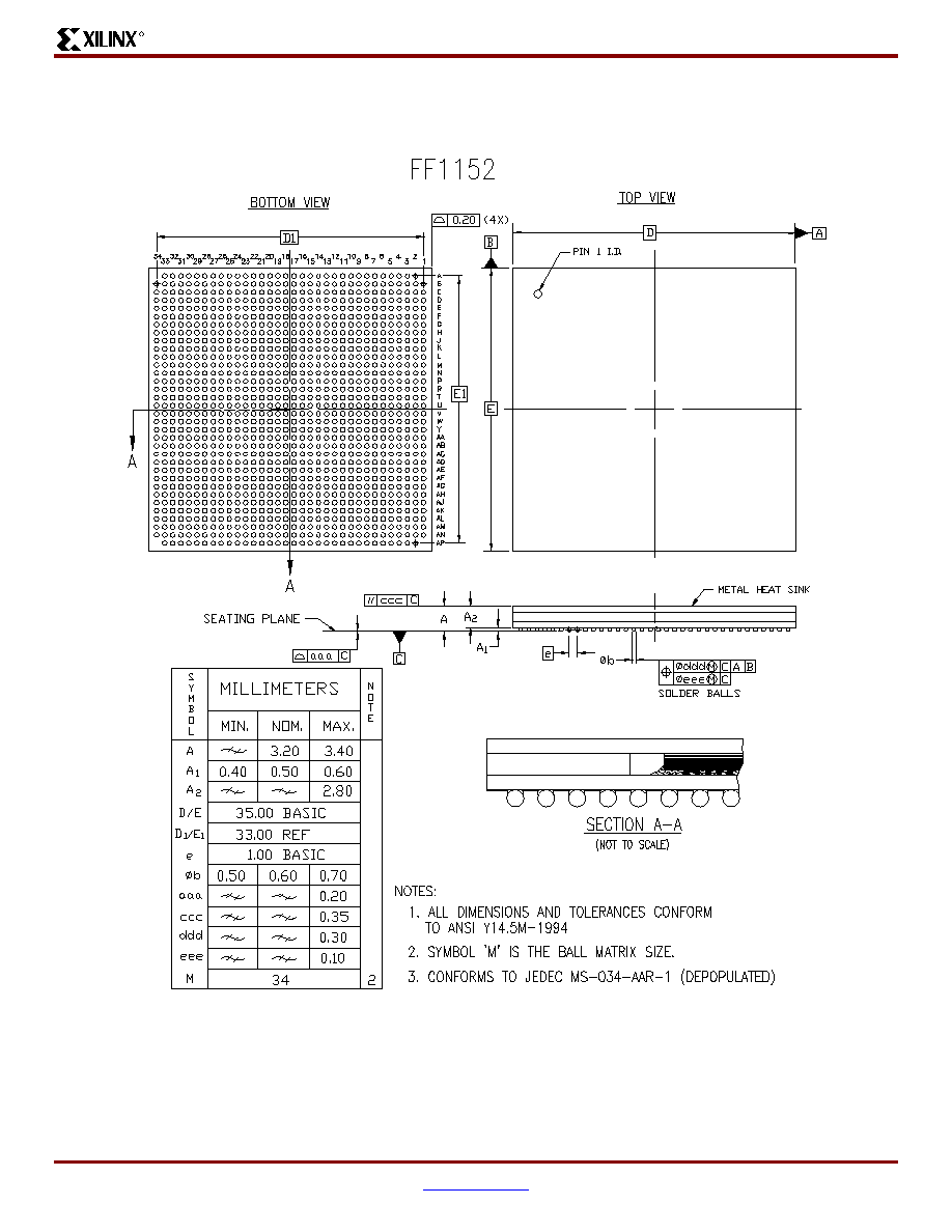
Virtex-II ProTM Platform FPGAs: Pinout Information
R
DS083-4 (v2.5.5) August 25, 2003
www.xilinx.com
127
Advance Product Specification
1-800-255-7778
FF1152 Flip-Chip Fine-Pitch BGA Package Specifications (1.00mm pitch)
Figure 6: FF1152 Flip-Chip Fine-Pitch BGA Package Specifications
FF1148 Flip-Chip Fine-Pitch BGA Package
R
128
www.xilinx.com
DS083-4 (v2.5.5) August 25, 2003
1-800-255-7778
Advance Product Specification
FF1148 Flip-Chip Fine-Pitch BGA Package
As shown in
Table 11
, XC2VP40 and XC2VP50 Virtex-II Pro devices are available in the FF1148 flip-chip fine-pitch BGA
package. Pins in each of these devices are the same, except for the differences shown in the No Connect column. Following
this table are the
FF1148 Flip-Chip Fine-Pitch BGA Package Specifications (1.00mm pitch)
.
Table 11: FF1148 -- XC2VP40 and XC2VP50
Bank
Pin Description
Pin Number
No Connects
XC2VP40
XC2VP50
0
IO_L01N_0/VRP_0
E25
0
IO_L01P_0/VRN_0
F25
0
IO_L02N_0
J24
0
IO_L02P_0
K24
0
IO_L03N_0
C25
0
IO_L03P_0/VREF_0
D25
0
IO_L05_0/No_Pair
G25
0
IO_L06N_0
A25
0
IO_L06P_0
B25
0
IO_L07N_0
G24
0
IO_L07P_0
G23
0
IO_L08N_0
H23
0
IO_L08P_0
H22
0
IO_L09N_0
E24
0
IO_L09P_0/VREF_0
F24
0
IO_L19N_0
C24
0
IO_L19P_0
C23
0
IO_L20N_0
J23
0
IO_L20P_0
K23
0
IO_L21N_0
A24
0
IO_L21P_0
B24
0
IO_L25N_0
E23
0
IO_L25P_0
F23
0
IO_L26N_0
K22
0
IO_L26P_0
L22
0
IO_L27N_0
D23
0
IO_L27P_0/VREF_0
D22
0
IO_L37N_0
A23
0
IO_L37P_0
B23
0
IO_L38N_0
J21
0
IO_L38P_0
J20
0
IO_L39N_0
F22
0
IO_L39P_0
G22
Virtex-II ProTM Platform FPGAs: Pinout Information
R
DS083-4 (v2.5.5) August 25, 2003
www.xilinx.com
129
Advance Product Specification
1-800-255-7778
0
IO_L43N_0
B22
0
IO_L43P_0
C22
0
IO_L44N_0
K21
0
IO_L44P_0
L21
0
IO_L45N_0
G21
0
IO_L45P_0/VREF_0
H21
0
IO_L46N_0
E21
0
IO_L46P_0
F21
0
IO_L47N_0
K20
0
IO_L47P_0
L20
0
IO_L48N_0
C21
0
IO_L48P_0
D21
0
IO_L49N_0
A21
0
IO_L49P_0
B21
0
IO_L50_0/No_Pair
G20
0
IO_L53_0/No_Pair
H19
0
IO_L54N_0
E20
0
IO_L54P_0
F20
0
IO_L55N_0
C20
0
IO_L55P_0
D19
0
IO_L56N_0
K19
0
IO_L56P_0
L19
0
IO_L57N_0
A20
0
IO_L57P_0/VREF_0
B20
0
IO_L66N_0
F19
NC
0
IO_L66P_0/VREF_0
G19
NC
0
IO_L67N_0
B19
0
IO_L67P_0
C19
0
IO_L68N_0
H18
0
IO_L68P_0
J18
0
IO_L69N_0
F18
0
IO_L69P_0/VREF_0
G18
0
IO_L73N_0
D18
0
IO_L73P_0
E18
0
IO_L74N_0/GCLK7P
K18
0
IO_L74P_0/GCLK6S
L18
0
IO_L75N_0/GCLK5P
B18
0
IO_L75P_0/GCLK4S
C18
Table 11: FF1148 -- XC2VP40 and XC2VP50
Bank
Pin Description
Pin Number
No Connects
XC2VP40
XC2VP50
FF1148 Flip-Chip Fine-Pitch BGA Package
R
130
www.xilinx.com
DS083-4 (v2.5.5) August 25, 2003
1-800-255-7778
Advance Product Specification
1
IO_L75N_1/GCLK3P
C17
1
IO_L75P_1/GCLK2S
B17
1
IO_L74N_1/GCLK1P
L17
1
IO_L74P_1/GCLK0S
K17
1
IO_L73N_1
E17
1
IO_L73P_1
D17
1
IO_L69N_1/VREF_1
G17
1
IO_L69P_1
F17
1
IO_L68N_1
J17
1
IO_L68P_1
H17
1
IO_L67N_1
C16
1
IO_L67P_1
B16
1
IO_L66N_1/VREF_1
G16
NC
1
IO_L66P_1
F16
NC
1
IO_L57N_1/VREF_1
B15
1
IO_L57P_1
A15
1
IO_L56N_1
L16
1
IO_L56P_1
K16
1
IO_L55N_1
D16
1
IO_L55P_1
C15
1
IO_L54N_1
F15
1
IO_L54P_1
E15
1
IO_L53_1/No_Pair
H16
1
IO_L50_1/No_Pair
G15
1
IO_L49N_1
B14
1
IO_L49P_1
A14
1
IO_L48N_1
D14
1
IO_L48P_1
C14
1
IO_L47N_1
L15
1
IO_L47P_1
K15
1
IO_L46N_1
F14
1
IO_L46P_1
E14
1
IO_L45N_1/VREF_1
H14
1
IO_L45P_1
G14
1
IO_L44N_1
L14
1
IO_L44P_1
K14
1
IO_L43N_1
C13
Table 11: FF1148 -- XC2VP40 and XC2VP50
Bank
Pin Description
Pin Number
No Connects
XC2VP40
XC2VP50
Virtex-II ProTM Platform FPGAs: Pinout Information
R
DS083-4 (v2.5.5) August 25, 2003
www.xilinx.com
131
Advance Product Specification
1-800-255-7778
1
IO_L43P_1
B13
1
IO_L39N_1
G13
1
IO_L39P_1
F13
1
IO_L38N_1
J15
1
IO_L38P_1
J14
1
IO_L37N_1
B12
1
IO_L37P_1
A12
1
IO_L27N_1/VREF_1
D13
1
IO_L27P_1
D12
1
IO_L26N_1
L13
1
IO_L26P_1
K13
1
IO_L25N_1
F12
1
IO_L25P_1
E12
1
IO_L21N_1
B11
1
IO_L21P_1
A11
1
IO_L20N_1
K12
1
IO_L20P_1
J12
1
IO_L19N_1
C12
1
IO_L19P_1
C11
1
IO_L09N_1/VREF_1
F11
1
IO_L09P_1
E11
1
IO_L08N_1
H13
1
IO_L08P_1
H12
1
IO_L07N_1
G12
1
IO_L07P_1
G11
1
IO_L06N_1
B10
1
IO_L06P_1
A10
1
IO_L05_1/No_Pair
G10
1
IO_L03N_1/VREF_1
D10
1
IO_L03P_1
C10
1
IO_L02N_1
K11
1
IO_L02P_1
J11
1
IO_L01N_1/VRP_1
F10
1
IO_L01P_1/VRN_1
E10
2
IO_L01N_2/VRP_2
B8
2
IO_L01P_2/VRN_2
B9
2
IO_L02N_2
C9
Table 11: FF1148 -- XC2VP40 and XC2VP50
Bank
Pin Description
Pin Number
No Connects
XC2VP40
XC2VP50

FF1148 Flip-Chip Fine-Pitch BGA Package
R
132
www.xilinx.com
DS083-4 (v2.5.5) August 25, 2003
1-800-255-7778
Advance Product Specification
2
IO_L02P_2
D9
2
IO_L03N_2
B7
2
IO_L03P_2
A7
2
IO_L04N_2/VREF_2
B6
2
IO_L04P_2
A6
2
IO_L05N_2
E8
2
IO_L05P_2
D8
2
IO_L06N_2
B4
2
IO_L06P_2
A4
2
IO_L07N_2
B3
2
IO_L07P_2
A3
2
IO_L08N_2
H7
2
IO_L08P_2
H8
2
IO_L09N_2
C6
2
IO_L09P_2
C7
2
IO_L10N_2/VREF_2
C5
2
IO_L10P_2
B5
2
IO_L11N_2
K8
2
IO_L11P_2
J8
2
IO_L12N_2
C1
2
IO_L12P_2
C2
2
IO_L13N_2
E7
2
IO_L13P_2
D7
2
IO_L14N_2
J6
2
IO_L14P_2
J7
2
IO_L15N_2
D5
2
IO_L15P_2
D6
2
IO_L16N_2/VREF_2
E4
2
IO_L16P_2
D4
2
IO_L17N_2
L9
2
IO_L17P_2
K9
2
IO_L18N_2
E3
2
IO_L18P_2
D3
2
IO_L19N_2
D1
2
IO_L19P_2
D2
2
IO_L20N_2
K7
2
IO_L20P_2
L7
2
IO_L21N_2
F6
Table 11: FF1148 -- XC2VP40 and XC2VP50
Bank
Pin Description
Pin Number
No Connects
XC2VP40
XC2VP50

Virtex-II ProTM Platform FPGAs: Pinout Information
R
DS083-4 (v2.5.5) August 25, 2003
www.xilinx.com
133
Advance Product Specification
1-800-255-7778
2
IO_L21P_2
E6
2
IO_L22N_2/VREF_2
F7
2
IO_L22P_2
F8
2
IO_L23N_2
M10
2
IO_L23P_2
L10
2
IO_L24N_2
G5
2
IO_L24P_2
F5
2
IO_L25N_2
F3
2
IO_L25P_2
F4
2
IO_L26N_2
M8
2
IO_L26P_2
M9
2
IO_L27N_2
F1
2
IO_L27P_2
F2
2
IO_L28N_2/VREF_2
G6
2
IO_L28P_2
G7
2
IO_L29N_2
M7
2
IO_L29P_2
N8
2
IO_L30N_2
G3
2
IO_L30P_2
H4
2
IO_L31N_2
G1
2
IO_L31P_2
G2
2
IO_L32N_2
N10
2
IO_L32P_2
N11
2
IO_L33N_2
H5
2
IO_L33P_2
H6
2
IO_L34N_2/VREF_2
H2
2
IO_L34P_2
H3
2
IO_L35N_2
N6
2
IO_L35P_2
N7
2
IO_L36N_2
K4
2
IO_L36P_2
J4
2
IO_L37N_2
J2
2
IO_L37P_2
J3
2
IO_L38N_2
P10
2
IO_L38P_2
P11
2
IO_L39N_2
K5
2
IO_L39P_2
K6
2
IO_L40N_2/VREF_2
L3
Table 11: FF1148 -- XC2VP40 and XC2VP50
Bank
Pin Description
Pin Number
No Connects
XC2VP40
XC2VP50

FF1148 Flip-Chip Fine-Pitch BGA Package
R
134
www.xilinx.com
DS083-4 (v2.5.5) August 25, 2003
1-800-255-7778
Advance Product Specification
2
IO_L40P_2
K3
2
IO_L41N_2
R9
2
IO_L41P_2
P9
2
IO_L42N_2
K1
2
IO_L42P_2
K2
2
IO_L43N_2
L5
2
IO_L43P_2
L6
2
IO_L44N_2
P7
2
IO_L44P_2
P8
2
IO_L45N_2
L1
2
IO_L45P_2
L2
2
IO_L46N_2/VREF_2
M5
2
IO_L46P_2
M6
2
IO_L47N_2
R10
2
IO_L47P_2
R11
2
IO_L48N_2
M3
2
IO_L48P_2
M4
2
IO_L49N_2
M1
2
IO_L49P_2
M2
2
IO_L50N_2
R7
2
IO_L50P_2
T8
2
IO_L51N_2
P4
2
IO_L51P_2
N4
2
IO_L52N_2/VREF_2
N2
2
IO_L52P_2
N3
2
IO_L53N_2
T10
2
IO_L53P_2
T11
2
IO_L54N_2
P5
2
IO_L54P_2
P6
2
IO_L55N_2
R3
2
IO_L55P_2
P3
2
IO_L56N_2
T6
2
IO_L56P_2
T7
2
IO_L57N_2
P1
2
IO_L57P_2
P2
2
IO_L58N_2/VREF_2
R5
2
IO_L58P_2
R6
2
IO_L59N_2
U10
Table 11: FF1148 -- XC2VP40 and XC2VP50
Bank
Pin Description
Pin Number
No Connects
XC2VP40
XC2VP50
Virtex-II ProTM Platform FPGAs: Pinout Information
R
DS083-4 (v2.5.5) August 25, 2003
www.xilinx.com
135
Advance Product Specification
1-800-255-7778
2
IO_L59P_2
U11
2
IO_L60N_2
R1
2
IO_L60P_2
R2
2
IO_L85N_2
T3
2
IO_L85P_2
T4
2
IO_L86N_2
U8
2
IO_L86P_2
U9
2
IO_L87N_2
U2
2
IO_L87P_2
T2
2
IO_L88N_2/VREF_2
U4
2
IO_L88P_2
U5
2
IO_L89N_2
U6
2
IO_L89P_2
U7
2
IO_L90N_2
V3
2
IO_L90P_2
U3
3
IO_L90N_3
V6
3
IO_L90P_3
V7
3
IO_L89N_3
V10
3
IO_L89P_3
V11
3
IO_L88N_3
V4
3
IO_L88P_3
V5
3
IO_L87N_3/VREF_3
V2
3
IO_L87P_3
W2
3
IO_L86N_3
V8
3
IO_L86P_3
V9
3
IO_L85N_3
W6
3
IO_L85P_3
W7
3
IO_L60N_3
W3
3
IO_L60P_3
W4
3
IO_L59N_3
W10
3
IO_L59P_3
W11
3
IO_L58N_3
Y5
3
IO_L58P_3
Y6
3
IO_L57N_3/VREF_3
Y3
3
IO_L57P_3
AA3
3
IO_L56N_3
W8
3
IO_L56P_3
Y7
Table 11: FF1148 -- XC2VP40 and XC2VP50
Bank
Pin Description
Pin Number
No Connects
XC2VP40
XC2VP50
FF1148 Flip-Chip Fine-Pitch BGA Package
R
136
www.xilinx.com
DS083-4 (v2.5.5) August 25, 2003
1-800-255-7778
Advance Product Specification
3
IO_L55N_3
Y1
3
IO_L55P_3
Y2
3
IO_L54N_3
AA5
3
IO_L54P_3
AA6
3
IO_L53N_3
Y10
3
IO_L53P_3
Y11
3
IO_L52N_3
AA4
3
IO_L52P_3
AB4
3
IO_L51N_3/VREF_3
AA1
3
IO_L51P_3
AA2
3
IO_L50N_3
Y9
3
IO_L50P_3
AA9
3
IO_L49N_3
AB6
3
IO_L49P_3
AB7
3
IO_L48N_3
AB2
3
IO_L48P_3
AB3
3
IO_L47N_3
AA10
3
IO_L47P_3
AA11
3
IO_L46N_3
AC5
3
IO_L46P_3
AC6
3
IO_L45N_3/VREF_3
AC3
3
IO_L45P_3
AC4
3
IO_L44N_3
AA7
3
IO_L44P_3
AA8
3
IO_L43N_3
AC1
3
IO_L43P_3
AC2
3
IO_L42N_3
AD5
3
IO_L42P_3
AD6
3
IO_L41N_3
AB10
3
IO_L41P_3
AB11
3
IO_L40N_3
AD3
3
IO_L40P_3
AE3
3
IO_L39N_3/VREF_3
AD1
3
IO_L39P_3
AD2
3
IO_L38N_3
AB8
3
IO_L38P_3
AC7
3
IO_L37N_3
AE5
3
IO_L37P_3
AE6
Table 11: FF1148 -- XC2VP40 and XC2VP50
Bank
Pin Description
Pin Number
No Connects
XC2VP40
XC2VP50

Virtex-II ProTM Platform FPGAs: Pinout Information
R
DS083-4 (v2.5.5) August 25, 2003
www.xilinx.com
137
Advance Product Specification
1-800-255-7778
3
IO_L36N_3
AE4
3
IO_L36P_3
AF4
3
IO_L35N_3
AC10
3
IO_L35P_3
AD10
3
IO_L34N_3
AE1
3
IO_L34P_3
AE2
3
IO_L33N_3/VREF_3
AF6
3
IO_L33P_3
AF7
3
IO_L32N_3
AC8
3
IO_L32P_3
AC9
3
IO_L31N_3
AF2
3
IO_L31P_3
AF3
3
IO_L30N_3
AG5
3
IO_L30P_3
AG6
3
IO_L29N_3
AD9
3
IO_L29P_3
AE9
3
IO_L28N_3
AG4
3
IO_L28P_3
AH3
3
IO_L27N_3/VREF_3
AG2
3
IO_L27P_3
AG3
3
IO_L26N_3
AD7
3
IO_L26P_3
AE7
3
IO_L25N_3
AH6
3
IO_L25P_3
AH7
3
IO_L24N_3
AH5
3
IO_L24P_3
AJ5
3
IO_L23N_3
AE8
3
IO_L23P_3
AF8
3
IO_L22N_3
AH1
3
IO_L22P_3
AH2
3
IO_L21N_3/VREF_3
AJ6
3
IO_L21P_3
AK6
3
IO_L20N_3
AG7
3
IO_L20P_3
AG8
3
IO_L19N_3
AJ3
3
IO_L19P_3
AJ4
3
IO_L18N_3
AJ1
3
IO_L18P_3
AJ2
Table 11: FF1148 -- XC2VP40 and XC2VP50
Bank
Pin Description
Pin Number
No Connects
XC2VP40
XC2VP50
FF1148 Flip-Chip Fine-Pitch BGA Package
R
138
www.xilinx.com
DS083-4 (v2.5.5) August 25, 2003
1-800-255-7778
Advance Product Specification
3
IO_L17N_3
AH9
3
IO_L17P_3
AJ9
3
IO_L16N_3
AK7
3
IO_L16P_3
AL7
3
IO_L15N_3/VREF_3
AK4
3
IO_L15P_3
AL4
3
IO_L14N_3
AJ7
3
IO_L14P_3
AJ8
3
IO_L13N_3
AK3
3
IO_L13P_3
AL3
3
IO_L12N_3
AL5
3
IO_L12P_3
AL6
3
IO_L11N_3
AK8
3
IO_L11P_3
AL8
3
IO_L10N_3
AL1
3
IO_L10P_3
AL2
3
IO_L09N_3/VREF_3
AM6
3
IO_L09P_3
AM7
3
IO_L08N_3
AL9
3
IO_L08P_3
AM9
3
IO_L07N_3
AM5
3
IO_L07P_3
AN5
3
IO_L06N_3
AM1
3
IO_L06P_3
AM2
3
IO_L05N_3
AN8
3
IO_L05P_3
AN9
3
IO_L04N_3
AN6
3
IO_L04P_3
AP6
3
IO_L03N_3/VREF_3
AN4
3
IO_L03P_3
AP4
3
IO_L02N_3
AN7
3
IO_L02P_3
AP7
3
IO_L01N_3/VRP_3
AN3
3
IO_L01P_3/VRN_3
AP3
4
IO_L01N_4/BUSY/DOUT
(1)
AK10
4
IO_L01P_4/INIT_B
AJ10
4
IO_L02N_4/D0/DIN
(1)
AF11
Table 11: FF1148 -- XC2VP40 and XC2VP50
Bank
Pin Description
Pin Number
No Connects
XC2VP40
XC2VP50
Virtex-II ProTM Platform FPGAs: Pinout Information
R
DS083-4 (v2.5.5) August 25, 2003
www.xilinx.com
139
Advance Product Specification
1-800-255-7778
4
IO_L02P_4/D1
AE11
4
IO_L03N_4/D2
AM10
4
IO_L03P_4/D3
AL10
4
IO_L05_4/No_Pair
AH10
4
IO_L06N_4/VRP_4
AP10
4
IO_L06P_4/VRN_4
AN10
4
IO_L07N_4
AH11
4
IO_L07P_4/VREF_4
AH12
4
IO_L08N_4
AG12
4
IO_L08P_4
AG13
4
IO_L09N_4
AK11
4
IO_L09P_4/VREF_4
AJ11
4
IO_L19N_4
AM11
4
IO_L19P_4
AM12
4
IO_L20N_4
AF12
4
IO_L20P_4
AE12
4
IO_L21N_4
AP11
4
IO_L21P_4
AN11
4
IO_L25N_4
AK12
4
IO_L25P_4
AJ12
4
IO_L26N_4
AE13
4
IO_L26P_4
AD13
4
IO_L27N_4
AL12
4
IO_L27P_4/VREF_4
AL13
4
IO_L37N_4
AP12
4
IO_L37P_4
AN12
4
IO_L38N_4
AF14
4
IO_L38P_4
AF15
4
IO_L39N_4
AJ13
4
IO_L39P_4
AH13
4
IO_L43N_4
AN13
4
IO_L43P_4
AM13
4
IO_L44N_4
AE14
4
IO_L44P_4
AD14
4
IO_L45N_4
AH14
4
IO_L45P_4/VREF_4
AG14
4
IO_L46N_4
AK14
4
IO_L46P_4
AJ14
Table 11: FF1148 -- XC2VP40 and XC2VP50
Bank
Pin Description
Pin Number
No Connects
XC2VP40
XC2VP50
FF1148 Flip-Chip Fine-Pitch BGA Package
R
140
www.xilinx.com
DS083-4 (v2.5.5) August 25, 2003
1-800-255-7778
Advance Product Specification
4
IO_L47N_4
AE15
4
IO_L47P_4
AD15
4
IO_L48N_4
AM14
4
IO_L48P_4
AL14
4
IO_L49N_4
AP14
4
IO_L49P_4
AN14
4
IO_L50_4/No_Pair
AH15
4
IO_L53_4/No_Pair
AG16
4
IO_L54N_4
AK15
4
IO_L54P_4
AJ15
4
IO_L55N_4
AM15
4
IO_L55P_4
AL16
4
IO_L56N_4
AE16
4
IO_L56P_4
AD16
4
IO_L57N_4
AP15
4
IO_L57P_4/VREF_4
AN15
4
IO_L66N_4
AJ16
NC
4
IO_L66P_4/VREF_4
AH16
NC
4
IO_L67N_4
AN16
4
IO_L67P_4
AM16
4
IO_L68N_4
AG17
4
IO_L68P_4
AF17
4
IO_L69N_4
AJ17
4
IO_L69P_4/VREF_4
AH17
4
IO_L73N_4
AL17
4
IO_L73P_4
AK17
4
IO_L74N_4/GCLK3S
AE17
4
IO_L74P_4/GCLK2P
AD17
4
IO_L75N_4/GCLK1S
AN17
4
IO_L75P_4/GCLK0P
AM17
5
IO_L75N_5/GCLK7S
AM18
5
IO_L75P_5/GCLK6P
AN18
5
IO_L74N_5/GCLK5S
AD18
5
IO_L74P_5/GCLK4P
AE18
5
IO_L73N_5
AK18
5
IO_L73P_5
AL18
5
IO_L69N_5/VREF_5
AH18
Table 11: FF1148 -- XC2VP40 and XC2VP50
Bank
Pin Description
Pin Number
No Connects
XC2VP40
XC2VP50

Virtex-II ProTM Platform FPGAs: Pinout Information
R
DS083-4 (v2.5.5) August 25, 2003
www.xilinx.com
141
Advance Product Specification
1-800-255-7778
5
IO_L69P_5
AJ18
5
IO_L68N_5
AF18
5
IO_L68P_5
AG18
5
IO_L67N_5
AM19
5
IO_L67P_5
AN19
5
IO_L66N_5/VREF_5
AH19
NC
5
IO_L66P_5
AJ19
NC
5
IO_L57N_5/VREF_5
AN20
5
IO_L57P_5
AP20
5
IO_L56N_5
AD19
5
IO_L56P_5
AE19
5
IO_L55N_5
AL19
5
IO_L55P_5
AM20
5
IO_L54N_5
AJ20
5
IO_L54P_5
AK20
5
IO_L53_5/No_Pair
AG19
5
IO_L50_5/No_Pair
AH20
5
IO_L49N_5
AN21
5
IO_L49P_5
AP21
5
IO_L48N_5
AL21
5
IO_L48P_5
AM21
5
IO_L47N_5
AD20
5
IO_L47P_5
AE20
5
IO_L46N_5
AJ21
5
IO_L46P_5
AK21
5
IO_L45N_5/VREF_5
AG21
5
IO_L45P_5
AH21
5
IO_L44N_5
AD21
5
IO_L44P_5
AE21
5
IO_L43N_5
AM22
5
IO_L43P_5
AN22
5
IO_L39N_5
AH22
5
IO_L39P_5
AJ22
5
IO_L38N_5
AF20
5
IO_L38P_5
AF21
5
IO_L37N_5
AN23
5
IO_L37P_5
AP23
5
IO_L27N_5/VREF_5
AL22
Table 11: FF1148 -- XC2VP40 and XC2VP50
Bank
Pin Description
Pin Number
No Connects
XC2VP40
XC2VP50
FF1148 Flip-Chip Fine-Pitch BGA Package
R
142
www.xilinx.com
DS083-4 (v2.5.5) August 25, 2003
1-800-255-7778
Advance Product Specification
5
IO_L27P_5
AL23
5
IO_L26N_5
AD22
5
IO_L26P_5
AE22
5
IO_L25N_5
AJ23
5
IO_L25P_5
AK23
5
IO_L21N_5
AN24
5
IO_L21P_5
AP24
5
IO_L20N_5
AE23
5
IO_L20P_5
AF23
5
IO_L19N_5
AM23
5
IO_L19P_5
AM24
5
IO_L09N_5/VREF_5
AJ24
5
IO_L09P_5
AK24
5
IO_L08N_5
AG22
5
IO_L08P_5
AG23
5
IO_L07N_5/VREF_5
AH23
5
IO_L07P_5
AH24
5
IO_L06N_5/VRP_5
AN25
5
IO_L06P_5/VRN_5
AP25
5
IO_L05_5/No_Pair
AH25
5
IO_L03N_5/D4
AL25
5
IO_L03P_5/D5
AM25
5
IO_L02N_5/D6
AE24
5
IO_L02P_5/D7
AF24
5
IO_L01N_5/RDWR_B
AJ25
5
IO_L01P_5/CS_B
AK25
6
IO_L01P_6/VRN_6
AP32
6
IO_L01N_6/VRP_6
AN32
6
IO_L02P_6
AP28
6
IO_L02N_6
AN28
6
IO_L03P_6
AP31
6
IO_L03N_6/VREF_6
AN31
6
IO_L04P_6
AP29
6
IO_L04N_6
AN29
6
IO_L05P_6
AN26
6
IO_L05N_6
AN27
6
IO_L06P_6
AM33
Table 11: FF1148 -- XC2VP40 and XC2VP50
Bank
Pin Description
Pin Number
No Connects
XC2VP40
XC2VP50

Virtex-II ProTM Platform FPGAs: Pinout Information
R
DS083-4 (v2.5.5) August 25, 2003
www.xilinx.com
143
Advance Product Specification
1-800-255-7778
6
IO_L06N_6
AM34
6
IO_L07P_6
AN30
6
IO_L07N_6
AM30
6
IO_L08P_6
AM26
6
IO_L08N_6
AL26
6
IO_L09P_6
AM28
6
IO_L09N_6/VREF_6
AM29
6
IO_L10P_6
AL33
6
IO_L10N_6
AL34
6
IO_L11P_6
AL27
6
IO_L11N_6
AK27
6
IO_L12P_6
AL29
6
IO_L12N_6
AL30
6
IO_L13P_6
AL32
6
IO_L13N_6
AK32
6
IO_L14P_6
AJ27
6
IO_L14N_6
AJ28
6
IO_L15P_6
AL31
6
IO_L15N_6/VREF_6
AK31
6
IO_L16P_6
AL28
6
IO_L16N_6
AK28
6
IO_L17P_6
AJ26
6
IO_L17N_6
AH26
6
IO_L18P_6
AJ33
6
IO_L18N_6
AJ34
6
IO_L19P_6
AJ31
6
IO_L19N_6
AJ32
6
IO_L20P_6
AG27
6
IO_L20N_6
AG28
6
IO_L21P_6
AK29
6
IO_L21N_6/VREF_6
AJ29
6
IO_L22P_6
AH33
6
IO_L22N_6
AH34
6
IO_L23P_6
AF27
6
IO_L23N_6
AE27
6
IO_L24P_6
AJ30
6
IO_L24N_6
AH30
6
IO_L25P_6
AH28
Table 11: FF1148 -- XC2VP40 and XC2VP50
Bank
Pin Description
Pin Number
No Connects
XC2VP40
XC2VP50

FF1148 Flip-Chip Fine-Pitch BGA Package
R
144
www.xilinx.com
DS083-4 (v2.5.5) August 25, 2003
1-800-255-7778
Advance Product Specification
6
IO_L25N_6
AH29
6
IO_L26P_6
AE28
6
IO_L26N_6
AD28
6
IO_L27P_6
AG32
6
IO_L27N_6/VREF_6
AG33
6
IO_L28P_6
AH32
6
IO_L28N_6
AG31
6
IO_L29P_6
AE26
6
IO_L29N_6
AD26
6
IO_L30P_6
AG29
6
IO_L30N_6
AG30
6
IO_L31P_6
AF32
6
IO_L31N_6
AF33
6
IO_L32P_6
AC26
6
IO_L32N_6
AC27
6
IO_L33P_6
AF28
6
IO_L33N_6/VREF_6
AF29
6
IO_L34P_6
AE33
6
IO_L34N_6
AE34
6
IO_L35P_6
AD25
6
IO_L35N_6
AC25
6
IO_L36P_6
AF31
6
IO_L36N_6
AE31
6
IO_L37P_6
AE29
6
IO_L37N_6
AE30
6
IO_L38P_6
AC28
6
IO_L38N_6
AB27
6
IO_L39P_6
AD33
6
IO_L39N_6/VREF_6
AD34
6
IO_L40P_6
AE32
6
IO_L40N_6
AD32
6
IO_L41P_6
AB24
6
IO_L41N_6
AB25
6
IO_L42P_6
AD29
6
IO_L42N_6
AD30
6
IO_L43P_6
AC33
6
IO_L43N_6
AC34
6
IO_L44P_6
AA27
Table 11: FF1148 -- XC2VP40 and XC2VP50
Bank
Pin Description
Pin Number
No Connects
XC2VP40
XC2VP50

Virtex-II ProTM Platform FPGAs: Pinout Information
R
DS083-4 (v2.5.5) August 25, 2003
www.xilinx.com
145
Advance Product Specification
1-800-255-7778
6
IO_L44N_6
AA28
6
IO_L45P_6
AC31
6
IO_L45N_6/VREF_6
AC32
6
IO_L46P_6
AC29
6
IO_L46N_6
AC30
6
IO_L47P_6
AA24
6
IO_L47N_6
AA25
6
IO_L48P_6
AB32
6
IO_L48N_6
AB33
6
IO_L49P_6
AB28
6
IO_L49N_6
AB29
6
IO_L50P_6
AA26
6
IO_L50N_6
Y26
6
IO_L51P_6
AA33
6
IO_L51N_6/VREF_6
AA34
6
IO_L52P_6
AB31
6
IO_L52N_6
AA31
6
IO_L53P_6
Y24
6
IO_L53N_6
Y25
6
IO_L54P_6
AA29
6
IO_L54N_6
AA30
6
IO_L55P_6
Y33
6
IO_L55N_6
Y34
6
IO_L56P_6
Y28
6
IO_L56N_6
W27
6
IO_L57P_6
AA32
6
IO_L57N_6/VREF_6
Y32
6
IO_L58P_6
Y29
6
IO_L58N_6
Y30
6
IO_L59P_6
W24
6
IO_L59N_6
W25
6
IO_L60P_6
W31
6
IO_L60N_6
W32
6
IO_L85P_6
W28
6
IO_L85N_6
W29
6
IO_L86P_6
V26
6
IO_L86N_6
V27
6
IO_L87P_6
W33
Table 11: FF1148 -- XC2VP40 and XC2VP50
Bank
Pin Description
Pin Number
No Connects
XC2VP40
XC2VP50
FF1148 Flip-Chip Fine-Pitch BGA Package
R
146
www.xilinx.com
DS083-4 (v2.5.5) August 25, 2003
1-800-255-7778
Advance Product Specification
6
IO_L87N_6/VREF_6
V33
6
IO_L88P_6
V30
6
IO_L88N_6
V31
6
IO_L89P_6
V24
6
IO_L89N_6
V25
6
IO_L90P_6
V28
6
IO_L90N_6
V29
7
IO_L90P_7
U32
7
IO_L90N_7
V32
7
IO_L89P_7
U28
7
IO_L89N_7
U29
7
IO_L88P_7
U30
7
IO_L88N_7/VREF_7
U31
7
IO_L87P_7
T33
7
IO_L87N_7
U33
7
IO_L86P_7
U26
7
IO_L86N_7
U27
7
IO_L85P_7
T31
7
IO_L85N_7
T32
7
IO_L60P_7
R33
7
IO_L60N_7
R34
7
IO_L59P_7
U24
7
IO_L59N_7
U25
7
IO_L58P_7
R29
7
IO_L58N_7/VREF_7
R30
7
IO_L57P_7
P33
7
IO_L57N_7
P34
7
IO_L56P_7
T28
7
IO_L56N_7
T29
7
IO_L55P_7
P32
7
IO_L55N_7
R32
7
IO_L54P_7
P29
7
IO_L54N_7
P30
7
IO_L53P_7
T24
7
IO_L53N_7
T25
7
IO_L52P_7
N32
7
IO_L52N_7/VREF_7
N33
Table 11: FF1148 -- XC2VP40 and XC2VP50
Bank
Pin Description
Pin Number
No Connects
XC2VP40
XC2VP50

Virtex-II ProTM Platform FPGAs: Pinout Information
R
DS083-4 (v2.5.5) August 25, 2003
www.xilinx.com
147
Advance Product Specification
1-800-255-7778
7
IO_L51P_7
N31
7
IO_L51N_7
P31
7
IO_L50P_7
T27
7
IO_L50N_7
R28
7
IO_L49P_7
M33
7
IO_L49N_7
M34
7
IO_L48P_7
M31
7
IO_L48N_7
M32
7
IO_L47P_7
R24
7
IO_L47N_7
R25
7
IO_L46P_7
M29
7
IO_L46N_7/VREF_7
M30
7
IO_L45P_7
L33
7
IO_L45N_7
L34
7
IO_L44P_7
P27
7
IO_L44N_7
P28
7
IO_L43P_7
L29
7
IO_L43N_7
L30
7
IO_L42P_7
K33
7
IO_L42N_7
K34
7
IO_L41P_7
P26
7
IO_L41N_7
R26
7
IO_L40P_7
K32
7
IO_L40N_7/VREF_7
L32
7
IO_L39P_7
K29
7
IO_L39N_7
K30
7
IO_L38P_7
P24
7
IO_L38N_7
P25
7
IO_L37P_7
J32
7
IO_L37N_7
J33
7
IO_L36P_7
J31
7
IO_L36N_7
K31
7
IO_L35P_7
N28
7
IO_L35N_7
N29
7
IO_L34P_7
H32
7
IO_L34N_7/VREF_7
H33
7
IO_L33P_7
H29
7
IO_L33N_7
H30
Table 11: FF1148 -- XC2VP40 and XC2VP50
Bank
Pin Description
Pin Number
No Connects
XC2VP40
XC2VP50

FF1148 Flip-Chip Fine-Pitch BGA Package
R
148
www.xilinx.com
DS083-4 (v2.5.5) August 25, 2003
1-800-255-7778
Advance Product Specification
7
IO_L32P_7
N24
7
IO_L32N_7
N25
7
IO_L31P_7
G33
7
IO_L31N_7
G34
7
IO_L30P_7
H31
7
IO_L30N_7
G32
7
IO_L29P_7
N27
7
IO_L29N_7
M28
7
IO_L28P_7
G28
7
IO_L28N_7/VREF_7
G29
7
IO_L27P_7
F33
7
IO_L27N_7
F34
7
IO_L26P_7
M26
7
IO_L26N_7
M27
7
IO_L25P_7
F31
7
IO_L25N_7
F32
7
IO_L24P_7
F30
7
IO_L24N_7
G30
7
IO_L23P_7
L25
7
IO_L23N_7
M25
7
IO_L22P_7
F27
7
IO_L22N_7/VREF_7
F28
7
IO_L21P_7
E29
7
IO_L21N_7
F29
7
IO_L20P_7
L28
7
IO_L20N_7
K28
7
IO_L19P_7
D33
7
IO_L19N_7
D34
7
IO_L18P_7
D32
7
IO_L18N_7
E32
7
IO_L17P_7
K26
7
IO_L17N_7
L26
7
IO_L16P_7
D31
7
IO_L16N_7/VREF_7
E31
7
IO_L15P_7
D29
7
IO_L15N_7
D30
7
IO_L14P_7
J28
7
IO_L14N_7
J29
Table 11: FF1148 -- XC2VP40 and XC2VP50
Bank
Pin Description
Pin Number
No Connects
XC2VP40
XC2VP50
Virtex-II ProTM Platform FPGAs: Pinout Information
R
DS083-4 (v2.5.5) August 25, 2003
www.xilinx.com
149
Advance Product Specification
1-800-255-7778
7
IO_L13P_7
D28
7
IO_L13N_7
E28
7
IO_L12P_7
C33
7
IO_L12N_7
C34
7
IO_L11P_7
J27
7
IO_L11N_7
K27
7
IO_L10P_7
B30
7
IO_L10N_7/VREF_7
C30
7
IO_L09P_7
C28
7
IO_L09N_7
C29
7
IO_L08P_7
H27
7
IO_L08N_7
H28
7
IO_L07P_7
A32
7
IO_L07N_7
B32
7
IO_L06P_7
A31
7
IO_L06N_7
B31
7
IO_L05P_7
D27
7
IO_L05N_7
E27
7
IO_L04P_7
A29
7
IO_L04N_7/VREF_7
B29
7
IO_L03P_7
A28
7
IO_L03N_7
B28
7
IO_L02P_7
D26
7
IO_L02N_7
C26
7
IO_L01P_7/VRN_7
B26
7
IO_L01N_7/VRP_7
B27
7
VCCO_7
E33
7
VCCO_7
R31
7
VCCO_7
L31
7
VCCO_7
G31
7
VCCO_7
C31
7
VCCO_7
R27
7
VCCO_7
L27
7
VCCO_7
G27
7
VCCO_7
C27
7
VCCO_7
J26
7
VCCO_7
M24
Table 11: FF1148 -- XC2VP40 and XC2VP50
Bank
Pin Description
Pin Number
No Connects
XC2VP40
XC2VP50

FF1148 Flip-Chip Fine-Pitch BGA Package
R
150
www.xilinx.com
DS083-4 (v2.5.5) August 25, 2003
1-800-255-7778
Advance Product Specification
7
VCCO_7
U23
7
VCCO_7
T23
7
VCCO_7
R23
7
VCCO_7
P23
7
VCCO_7
N23
6
VCCO_6
AK33
6
VCCO_6
AM31
6
VCCO_6
AH31
6
VCCO_6
AD31
6
VCCO_6
Y31
6
VCCO_6
AM27
6
VCCO_6
AH27
6
VCCO_6
AD27
6
VCCO_6
Y27
6
VCCO_6
AF26
6
VCCO_6
AC24
6
VCCO_6
AB23
6
VCCO_6
AA23
6
VCCO_6
Y23
6
VCCO_6
W23
6
VCCO_6
V23
5
VCCO_5
AL24
5
VCCO_5
AG24
5
VCCO_5
AD23
5
VCCO_5
AC22
5
VCCO_5
AC21
5
VCCO_5
AL20
5
VCCO_5
AG20
5
VCCO_5
AC20
5
VCCO_5
AC19
5
VCCO_5
AC18
4
VCCO_4
AC17
4
VCCO_4
AC16
4
VCCO_4
AL15
4
VCCO_4
AG15
4
VCCO_4
AC15
4
VCCO_4
AC14
4
VCCO_4
AC13
Table 11: FF1148 -- XC2VP40 and XC2VP50
Bank
Pin Description
Pin Number
No Connects
XC2VP40
XC2VP50

Virtex-II ProTM Platform FPGAs: Pinout Information
R
DS083-4 (v2.5.5) August 25, 2003
www.xilinx.com
151
Advance Product Specification
1-800-255-7778
4
VCCO_4
AD12
4
VCCO_4
AL11
4
VCCO_4
AG11
3
VCCO_3
AB12
3
VCCO_3
AA12
3
VCCO_3
Y12
3
VCCO_3
W12
3
VCCO_3
V12
3
VCCO_3
AC11
3
VCCO_3
AF9
3
VCCO_3
AM8
3
VCCO_3
AH8
3
VCCO_3
AD8
3
VCCO_3
Y8
3
VCCO_3
AM4
3
VCCO_3
AH4
3
VCCO_3
AD4
3
VCCO_3
Y4
3
VCCO_3
AK2
2
VCCO_2
U12
2
VCCO_2
T12
2
VCCO_2
R12
2
VCCO_2
P12
2
VCCO_2
N12
2
VCCO_2
M11
2
VCCO_2
J9
2
VCCO_2
R8
2
VCCO_2
L8
2
VCCO_2
G8
2
VCCO_2
C8
2
VCCO_2
R4
2
VCCO_2
L4
2
VCCO_2
G4
2
VCCO_2
C4
2
VCCO_2
E2
1
VCCO_1
M17
1
VCCO_1
M16
1
VCCO_1
M15
Table 11: FF1148 -- XC2VP40 and XC2VP50
Bank
Pin Description
Pin Number
No Connects
XC2VP40
XC2VP50
FF1148 Flip-Chip Fine-Pitch BGA Package
R
152
www.xilinx.com
DS083-4 (v2.5.5) August 25, 2003
1-800-255-7778
Advance Product Specification
1
VCCO_1
H15
1
VCCO_1
D15
1
VCCO_1
M14
1
VCCO_1
M13
1
VCCO_1
L12
1
VCCO_1
H11
1
VCCO_1
D11
0
VCCO_0
H24
0
VCCO_0
D24
0
VCCO_0
L23
0
VCCO_0
M22
0
VCCO_0
M21
0
VCCO_0
M20
0
VCCO_0
H20
0
VCCO_0
D20
0
VCCO_0
M19
0
VCCO_0
M18
N/A
CCLK
AG9
N/A
PROG_B
G26
N/A
DONE
AF10
N/A
M0
AG25
N/A
M1
AG26
N/A
M2
AF25
N/A
TCK
G9
N/A
TDI
F26
N/A
TDO
F9
N/A
TMS
H10
N/A
PWRDWN_B
AG10
N/A
HSWAP_EN
H25
N/A
RSVD
H9
N/A
VBATT
J10
N/A
DXP
J25
N/A
DXN
H26
N/A
VCCINT
AD24
N/A
VCCINT
L24
N/A
VCCINT
AC23
Table 11: FF1148 -- XC2VP40 and XC2VP50
Bank
Pin Description
Pin Number
No Connects
XC2VP40
XC2VP50

Virtex-II ProTM Platform FPGAs: Pinout Information
R
DS083-4 (v2.5.5) August 25, 2003
www.xilinx.com
153
Advance Product Specification
1-800-255-7778
N/A
VCCINT
M23
N/A
VCCINT
AB22
N/A
VCCINT
AA22
N/A
VCCINT
Y22
N/A
VCCINT
W22
N/A
VCCINT
V22
N/A
VCCINT
U22
N/A
VCCINT
T22
N/A
VCCINT
R22
N/A
VCCINT
P22
N/A
VCCINT
N22
N/A
VCCINT
AB21
N/A
VCCINT
N21
N/A
VCCINT
AB20
N/A
VCCINT
N20
N/A
VCCINT
AB19
N/A
VCCINT
N19
N/A
VCCINT
AB18
N/A
VCCINT
N18
N/A
VCCINT
AB17
N/A
VCCINT
N17
N/A
VCCINT
AB16
N/A
VCCINT
N16
N/A
VCCINT
AB15
N/A
VCCINT
N15
N/A
VCCINT
AB14
N/A
VCCINT
N14
N/A
VCCINT
AB13
N/A
VCCINT
AA13
N/A
VCCINT
Y13
N/A
VCCINT
W13
N/A
VCCINT
V13
N/A
VCCINT
U13
N/A
VCCINT
T13
N/A
VCCINT
R13
N/A
VCCINT
P13
N/A
VCCINT
N13
N/A
VCCINT
AC12
Table 11: FF1148 -- XC2VP40 and XC2VP50
Bank
Pin Description
Pin Number
No Connects
XC2VP40
XC2VP50

FF1148 Flip-Chip Fine-Pitch BGA Package
R
154
www.xilinx.com
DS083-4 (v2.5.5) August 25, 2003
1-800-255-7778
Advance Product Specification
N/A
VCCINT
M12
N/A
VCCINT
AD11
N/A
VCCINT
L11
N/A
VCCAUX
AN34
N/A
VCCAUX
AG34
N/A
VCCAUX
U34
N/A
VCCAUX
H34
N/A
VCCAUX
B34
N/A
VCCAUX
AP33
N/A
VCCAUX
A33
N/A
VCCAUX
AP27
N/A
VCCAUX
A27
N/A
VCCAUX
AP17
N/A
VCCAUX
A17
N/A
VCCAUX
AP8
N/A
VCCAUX
A8
N/A
VCCAUX
AP2
N/A
VCCAUX
A2
N/A
VCCAUX
AN1
N/A
VCCAUX
AG1
N/A
VCCAUX
U1
N/A
VCCAUX
H1
N/A
VCCAUX
B1
N/A
GND
AK34
N/A
GND
AF34
N/A
GND
AB34
N/A
GND
W34
N/A
GND
V34
N/A
GND
T34
N/A
GND
N34
N/A
GND
J34
N/A
GND
E34
N/A
GND
AN33
N/A
GND
B33
N/A
GND
AM32
N/A
GND
C32
N/A
GND
AP30
N/A
GND
AK30
Table 11: FF1148 -- XC2VP40 and XC2VP50
Bank
Pin Description
Pin Number
No Connects
XC2VP40
XC2VP50

Virtex-II ProTM Platform FPGAs: Pinout Information
R
DS083-4 (v2.5.5) August 25, 2003
www.xilinx.com
155
Advance Product Specification
1-800-255-7778
N/A
GND
AF30
N/A
GND
AB30
N/A
GND
W30
N/A
GND
T30
N/A
GND
N30
N/A
GND
J30
N/A
GND
E30
N/A
GND
A30
N/A
GND
AP26
N/A
GND
AK26
N/A
GND
AB26
N/A
GND
W26
N/A
GND
T26
N/A
GND
N26
N/A
GND
E26
N/A
GND
A26
N/A
GND
AE25
N/A
GND
K25
N/A
GND
AP22
N/A
GND
AK22
N/A
GND
AF22
N/A
GND
J22
N/A
GND
E22
N/A
GND
A22
N/A
GND
Y21
N/A
GND
W21
N/A
GND
V21
N/A
GND
U21
N/A
GND
T21
N/A
GND
R21
N/A
GND
AA20
N/A
GND
Y20
N/A
GND
W20
N/A
GND
V20
N/A
GND
U20
N/A
GND
T20
N/A
GND
R20
N/A
GND
P20
Table 11: FF1148 -- XC2VP40 and XC2VP50
Bank
Pin Description
Pin Number
No Connects
XC2VP40
XC2VP50

FF1148 Flip-Chip Fine-Pitch BGA Package
R
156
www.xilinx.com
DS083-4 (v2.5.5) August 25, 2003
1-800-255-7778
Advance Product Specification
N/A
GND
AP19
N/A
GND
AK19
N/A
GND
AF19
N/A
GND
AA19
N/A
GND
Y19
N/A
GND
W19
N/A
GND
V19
N/A
GND
U19
N/A
GND
T19
N/A
GND
R19
N/A
GND
P19
N/A
GND
J19
N/A
GND
E19
N/A
GND
A19
N/A
GND
AP18
N/A
GND
AA18
N/A
GND
Y18
N/A
GND
W18
N/A
GND
V18
N/A
GND
U18
N/A
GND
T18
N/A
GND
R18
N/A
GND
P18
N/A
GND
A18
N/A
GND
AA17
N/A
GND
Y17
N/A
GND
W17
N/A
GND
V17
N/A
GND
U17
N/A
GND
T17
N/A
GND
R17
N/A
GND
P17
N/A
GND
AP16
N/A
GND
AK16
N/A
GND
AF16
N/A
GND
AA16
N/A
GND
Y16
N/A
GND
W16
Table 11: FF1148 -- XC2VP40 and XC2VP50
Bank
Pin Description
Pin Number
No Connects
XC2VP40
XC2VP50

Virtex-II ProTM Platform FPGAs: Pinout Information
R
DS083-4 (v2.5.5) August 25, 2003
www.xilinx.com
157
Advance Product Specification
1-800-255-7778
N/A
GND
V16
N/A
GND
U16
N/A
GND
T16
N/A
GND
R16
N/A
GND
P16
N/A
GND
J16
N/A
GND
E16
N/A
GND
A16
N/A
GND
AA15
N/A
GND
Y15
N/A
GND
W15
N/A
GND
V15
N/A
GND
U15
N/A
GND
T15
N/A
GND
R15
N/A
GND
P15
N/A
GND
Y14
N/A
GND
W14
N/A
GND
V14
N/A
GND
U14
N/A
GND
T14
N/A
GND
R14
N/A
GND
AP13
N/A
GND
AK13
N/A
GND
AF13
N/A
GND
J13
N/A
GND
E13
N/A
GND
A13
N/A
GND
AE10
N/A
GND
K10
N/A
GND
AP9
N/A
GND
AK9
N/A
GND
AB9
N/A
GND
W9
N/A
GND
T9
N/A
GND
N9
N/A
GND
E9
N/A
GND
A9
Table 11: FF1148 -- XC2VP40 and XC2VP50
Bank
Pin Description
Pin Number
No Connects
XC2VP40
XC2VP50
FF1148 Flip-Chip Fine-Pitch BGA Package
R
158
www.xilinx.com
DS083-4 (v2.5.5) August 25, 2003
1-800-255-7778
Advance Product Specification
N/A
GND
AP5
N/A
GND
AK5
N/A
GND
AF5
N/A
GND
AB5
N/A
GND
W5
N/A
GND
T5
N/A
GND
N5
N/A
GND
J5
N/A
GND
E5
N/A
GND
A5
N/A
GND
AM3
N/A
GND
C3
N/A
GND
AN2
N/A
GND
B2
N/A
GND
AK1
N/A
GND
AF1
N/A
GND
AB1
N/A
GND
W1
N/A
GND
V1
N/A
GND
T1
N/A
GND
N1
N/A
GND
J1
N/A
GND
E1
Notes:
1.
See
Table 4
for an explanation of the signals available on this pin.
Table 11: FF1148 -- XC2VP40 and XC2VP50
Bank
Pin Description
Pin Number
No Connects
XC2VP40
XC2VP50
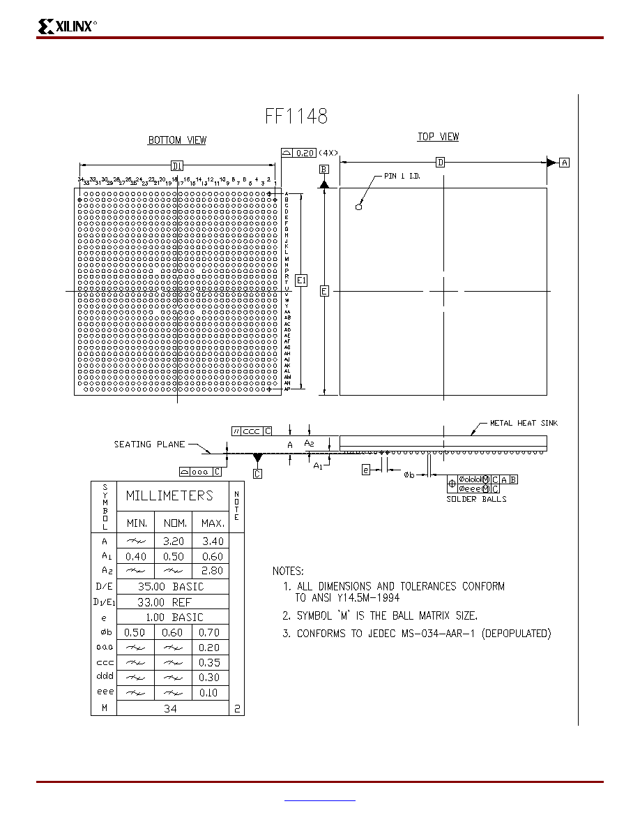
Virtex-II ProTM Platform FPGAs: Pinout Information
R
DS083-4 (v2.5.5) August 25, 2003
www.xilinx.com
159
Advance Product Specification
1-800-255-7778
FF1148 Flip-Chip Fine-Pitch BGA Package Specifications (1.00mm pitch)
Figure 7: FF1148 Flip-Chip Fine-Pitch BGA Package Specifications
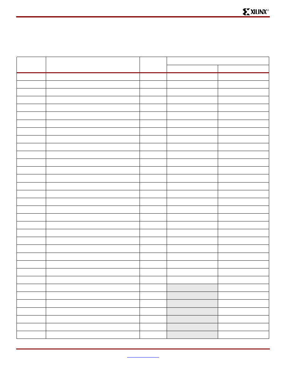
FF1517 Flip-Chip Fine-Pitch BGA Package
R
160
www.xilinx.com
DS083-4 (v2.5.5) August 25, 2003
1-800-255-7778
Advance Product Specification
FF1517 Flip-Chip Fine-Pitch BGA Package
As shown in
Table 12
, XC2VP50 and XC2VP70 Virtex-II Pro devices are available in the FF1517 flip-chip fine-pitch BGA
package. Following this table are the
FF1517 Flip-Chip Fine-Pitch BGA Package Specifications (1.00mm pitch)
.
Table 12: FF1517 -- XC2VP50 and XC2VP70
Bank
Pin Description
Pin
Number
No Connects
XC2VP50
XC2VP70
0
IO_L01N_0/VRP_0
D31
0
IO_L01P_0/VRN_0
E31
0
IO_L02N_0
K30
0
IO_L02P_0
J30
0
IO_L03N_0
G30
0
IO_L03P_0/VREF_0
H30
0
IO_L05_0/No_Pair
K28
0
IO_L06N_0
E30
0
IO_L06P_0
F30
0
IO_L07N_0
C30
0
IO_L07P_0
D30
0
IO_L08N_0
J29
0
IO_L08P_0
K29
0
IO_L09N_0
G29
0
IO_L09P_0/VREF_0
H29
0
IO_L19N_0
E29
0
IO_L19P_0
F29
0
IO_L20N_0
L28
0
IO_L20P_0
L27
0
IO_L21N_0
C29
0
IO_L21P_0
D29
0
IO_L25N_0
H28
0
IO_L25P_0
J28
0
IO_L26N_0
M27
0
IO_L26P_0
M26
0
IO_L27N_0
D28
0
IO_L27P_0/VREF_0
E28
0
IO_L28N_0
H27
NC
0
IO_L28P_0
J27
NC
0
IO_L29N_0
J26
NC
0
IO_L29P_0
K26
NC
0
IO_L30N_0
F28
NC
0
IO_L30P_0
G27
NC
0
IO_L34N_0
D27
NC

Virtex-II ProTM Platform FPGAs: Pinout Information
R
DS083-4 (v2.5.5) August 25, 2003
www.xilinx.com
161
Advance Product Specification
1-800-255-7778
0
IO_L34P_0
E27
NC
0
IO_L35N_0
L26
NC
0
IO_L35P_0
L25
NC
0
IO_L36N_0
G26
NC
0
IO_L36P_0/VREF_0
H26
NC
0
IO_L37N_0
E26
0
IO_L37P_0
F26
0
IO_L38N_0
K25
0
IO_L38P_0
K24
0
IO_L39N_0
C26
0
IO_L39P_0
D26
0
IO_L43N_0
H25
0
IO_L43P_0
J25
0
IO_L44N_0
M25
0
IO_L44P_0
M24
0
IO_L45N_0
F25
0
IO_L45P_0/VREF_0
G25
0
IO_L46N_0
C25
0
IO_L46P_0
D25
0
IO_L47N_0
L23
0
IO_L47P_0
M22
0
IO_L48N_0
H24
0
IO_L48P_0
J24
0
IO_L49N_0
E25
0
IO_L49P_0
E24
0
IO_L50_0/No_Pair
N23
0
IO_L53_0/No_Pair
M23
0
IO_L54N_0
H23
0
IO_L54P_0
J23
0
IO_L55N_0
F24
0
IO_L55P_0
G23
0
IO_L56N_0
K22
0
IO_L56P_0
L22
0
IO_L57N_0
C23
0
IO_L57P_0/VREF_0
D23
0
IO_L58N_0
H22
0
IO_L58P_0
J22
0
IO_L59N_0
N22
Table 12: FF1517 -- XC2VP50 and XC2VP70
Bank
Pin Description
Pin
Number
No Connects
XC2VP50
XC2VP70
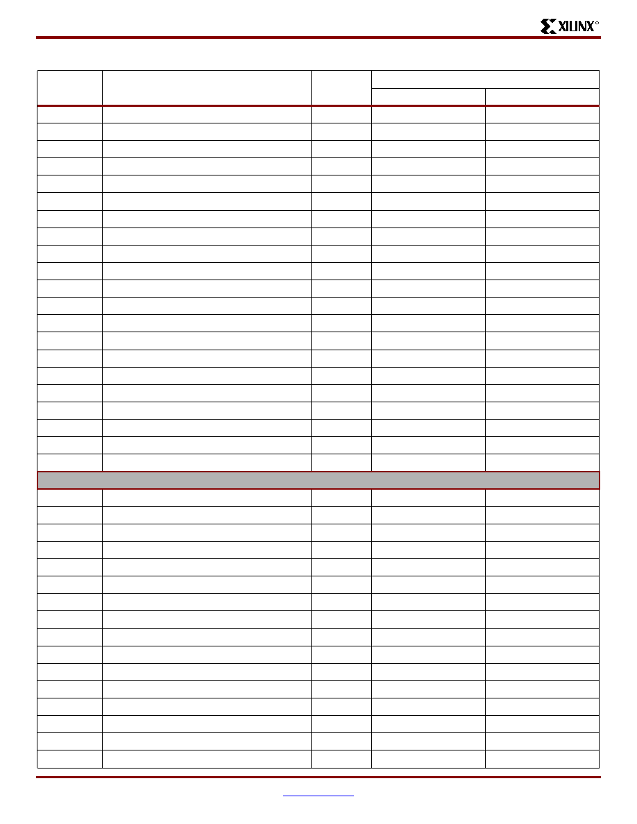
FF1517 Flip-Chip Fine-Pitch BGA Package
R
162
www.xilinx.com
DS083-4 (v2.5.5) August 25, 2003
1-800-255-7778
Advance Product Specification
0
IO_L59P_0
N21
0
IO_L60N_0
E23
0
IO_L60P_0
F22
0
IO_L64N_0
D22
0
IO_L64P_0
E22
0
IO_L65N_0
H21
0
IO_L65P_0
H20
0
IO_L66N_0
G22
0
IO_L66P_0/VREF_0
G21
0
IO_L67N_0
D21
0
IO_L67P_0
E21
0
IO_L68N_0
J21
0
IO_L68P_0
K21
0
IO_L69N_0
C22
0
IO_L69P_0/VREF_0
C21
0
IO_L73N_0
F21
0
IO_L73P_0
F20
0
IO_L74N_0/GCLK7P
L21
0
IO_L74P_0/GCLK6S
M21
0
IO_L75N_0/GCLK5P
D20
0
IO_L75P_0/GCLK4S
E20
1
IO_L75N_1/GCLK3P
K20
1
IO_L75P_1/GCLK2S
J20
1
IO_L74N_1/GCLK1P
N20
1
IO_L74P_1/GCLK0S
M20
1
IO_L73N_1
E19
1
IO_L73P_1
D19
1
IO_L69N_1/VREF_1
G19
1
IO_L69P_1
F19
1
IO_L68N_1
L19
1
IO_L68P_1
K19
1
IO_L67N_1
J19
1
IO_L67P_1
H19
1
IO_L66N_1/VREF_1
C19
1
IO_L66P_1
C18
1
IO_L65N_1
N19
1
IO_L65P_1
M19
Table 12: FF1517 -- XC2VP50 and XC2VP70
Bank
Pin Description
Pin
Number
No Connects
XC2VP50
XC2VP70

Virtex-II ProTM Platform FPGAs: Pinout Information
R
DS083-4 (v2.5.5) August 25, 2003
www.xilinx.com
163
Advance Product Specification
1-800-255-7778
1
IO_L64N_1
E18
1
IO_L64P_1
D18
1
IO_L60N_1
G18
1
IO_L60P_1
F18
1
IO_L59N_1
L18
1
IO_L59P_1
K18
1
IO_L58N_1
J18
1
IO_L58P_1
H18
1
IO_L57N_1/VREF_1
D17
1
IO_L57P_1
C17
1
IO_L56N_1
N18
1
IO_L56P_1
M18
1
IO_L55N_1
E17
1
IO_L55P_1
E16
1
IO_L54N_1
G17
1
IO_L54P_1
F16
1
IO_L53_1/No_Pair
J17
1
IO_L50_1/No_Pair
H17
1
IO_L49N_1
J16
1
IO_L49P_1
H16
1
IO_L48N_1
D15
1
IO_L48P_1
C15
1
IO_L47N_1
L17
1
IO_L47P_1
K16
1
IO_L46N_1
F15
1
IO_L46P_1
E15
1
IO_L45N_1/VREF_1
H15
1
IO_L45P_1
G15
1
IO_L44N_1
N17
1
IO_L44P_1
M17
1
IO_L43N_1
D14
1
IO_L43P_1
C14
1
IO_L39N_1
F14
1
IO_L39P_1
E14
1
IO_L38N_1
M16
1
IO_L38P_1
M15
1
IO_L37N_1
H14
1
IO_L37P_1
G14
Table 12: FF1517 -- XC2VP50 and XC2VP70
Bank
Pin Description
Pin
Number
No Connects
XC2VP50
XC2VP70
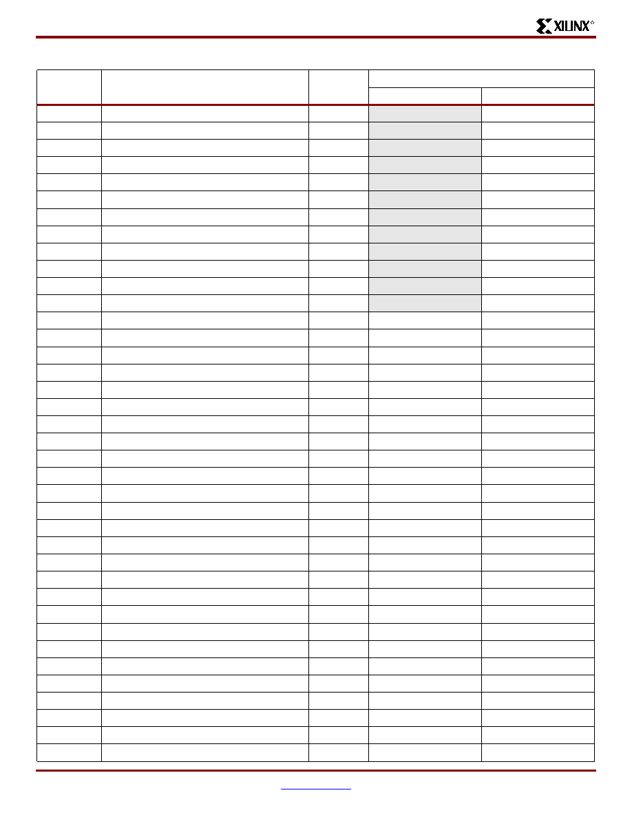
FF1517 Flip-Chip Fine-Pitch BGA Package
R
164
www.xilinx.com
DS083-4 (v2.5.5) August 25, 2003
1-800-255-7778
Advance Product Specification
1
IO_L36N_1/VREF_1
E13
NC
1
IO_L36P_1
D13
NC
1
IO_L35N_1
K15
NC
1
IO_L35P_1
J15
NC
1
IO_L34N_1
G13
NC
1
IO_L34P_1
F12
NC
1
IO_L30N_1
J13
NC
1
IO_L30P_1
H13
NC
1
IO_L29N_1
L15
NC
1
IO_L29P_1
L14
NC
1
IO_L28N_1
E12
NC
1
IO_L28P_1
D12
NC
1
IO_L27N_1/VREF_1
J12
1
IO_L27P_1
H12
1
IO_L26N_1
K14
1
IO_L26P_1
J14
1
IO_L25N_1
D11
1
IO_L25P_1
C11
1
IO_L21N_1
F11
1
IO_L21P_1
E11
1
IO_L20N_1
M14
1
IO_L20P_1
M13
1
IO_L19N_1
H11
1
IO_L19P_1
G11
1
IO_L09N_1/VREF_1
J11
1
IO_L09P_1
J10
1
IO_L08N_1
L13
1
IO_L08P_1
L12
1
IO_L07N_1
D10
1
IO_L07P_1
C10
1
IO_L06N_1
F10
1
IO_L06P_1
E10
1
IO_L05_1/No_Pair
K10
1
IO_L03N_1/VREF_1
H10
1
IO_L03P_1
G10
1
IO_L02N_1
K12
1
IO_L02P_1
K11
1
IO_L01N_1/VRP_1
E9
Table 12: FF1517 -- XC2VP50 and XC2VP70
Bank
Pin Description
Pin
Number
No Connects
XC2VP50
XC2VP70

Virtex-II ProTM Platform FPGAs: Pinout Information
R
DS083-4 (v2.5.5) August 25, 2003
www.xilinx.com
165
Advance Product Specification
1-800-255-7778
1
IO_L01P_1/VRN_1
D9
2
IO_L01N_2/VRP_2
C7
2
IO_L01P_2/VRN_2
D7
2
IO_L02N_2
G9
2
IO_L02P_2
H9
2
IO_L03N_2
C5
2
IO_L03P_2
D5
2
IO_L04N_2/VREF_2
D6
2
IO_L04P_2
E6
2
IO_L05N_2
H8
2
IO_L05P_2
J9
2
IO_L06N_2
E7
2
IO_L06P_2
F7
2
IO_L73N_2
D1
NC
2
IO_L73P_2
D2
NC
2
IO_L75N_2
E2
NC
2
IO_L75P_2
E3
NC
2
IO_L76N_2/VREF_2
F5
NC
2
IO_L76P_2
G5
NC
2
IO_L78N_2
F3
NC
2
IO_L78P_2
F4
NC
2
IO_L79N_2
F1
NC
2
IO_L79P_2
F2
NC
2
IO_L81N_2
G6
NC
2
IO_L81P_2
G7
NC
2
IO_L82N_2/VREF_2
G3
NC
2
IO_L82P_2
G4
NC
2
IO_L84N_2
G1
NC
2
IO_L84P_2
G2
NC
2
IO_L07N_2
H6
2
IO_L07P_2
H7
2
IO_L08N_2
K8
2
IO_L08P_2
K9
2
IO_L09N_2
H2
2
IO_L09P_2
H3
2
IO_L10N_2/VREF_2
J6
2
IO_L10P_2
J7
Table 12: FF1517 -- XC2VP50 and XC2VP70
Bank
Pin Description
Pin
Number
No Connects
XC2VP50
XC2VP70

FF1517 Flip-Chip Fine-Pitch BGA Package
R
166
www.xilinx.com
DS083-4 (v2.5.5) August 25, 2003
1-800-255-7778
Advance Product Specification
2
IO_L11N_2
L9
2
IO_L11P_2
M10
2
IO_L12N_2
H4
2
IO_L12P_2
J5
2
IO_L13N_2
J1
2
IO_L13P_2
J2
2
IO_L14N_2
M8
2
IO_L14P_2
N9
2
IO_L15N_2
K6
2
IO_L15P_2
K7
2
IO_L16N_2/VREF_2
K4
2
IO_L16P_2
K5
2
IO_L17N_2
P10
2
IO_L17P_2
N10
2
IO_L18N_2
K3
2
IO_L18P_2
J3
2
IO_L19N_2
K1
2
IO_L19P_2
K2
2
IO_L20N_2
M11
2
IO_L20P_2
N11
2
IO_L21N_2
L7
2
IO_L21P_2
L8
2
IO_L22N_2/VREF_2
L5
2
IO_L22P_2
L6
2
IO_L23N_2
P8
2
IO_L23P_2
P9
2
IO_L24N_2
L3
2
IO_L24P_2
L4
2
IO_L25N_2
L1
2
IO_L25P_2
L2
2
IO_L26N_2
P11
2
IO_L26P_2
P12
2
IO_L27N_2
M6
2
IO_L27P_2
M7
2
IO_L28N_2/VREF_2
M2
2
IO_L28P_2
M3
2
IO_L29N_2
R9
2
IO_L29P_2
R10
Table 12: FF1517 -- XC2VP50 and XC2VP70
Bank
Pin Description
Pin
Number
No Connects
XC2VP50
XC2VP70

Virtex-II ProTM Platform FPGAs: Pinout Information
R
DS083-4 (v2.5.5) August 25, 2003
www.xilinx.com
167
Advance Product Specification
1-800-255-7778
2
IO_L30N_2
N6
2
IO_L30P_2
N7
2
IO_L31N_2
M4
2
IO_L31P_2
N5
2
IO_L32N_2
R11
2
IO_L32P_2
R12
2
IO_L33N_2
N1
2
IO_L33P_2
N2
2
IO_L34N_2/VREF_2
P6
2
IO_L34P_2
P7
2
IO_L35N_2
R13
2
IO_L35P_2
T13
2
IO_L36N_2
P4
2
IO_L36P_2
P5
2
IO_L37N_2
P3
2
IO_L37P_2
N3
2
IO_L38N_2
T10
2
IO_L38P_2
T11
2
IO_L39N_2
P1
2
IO_L39P_2
P2
2
IO_L40N_2/VREF_2
R7
2
IO_L40P_2
R8
2
IO_L41N_2
T12
2
IO_L41P_2
U12
2
IO_L42N_2
R5
2
IO_L42P_2
R6
2
IO_L43N_2
R3
2
IO_L43P_2
R4
2
IO_L44N_2
U8
2
IO_L44P_2
T8
2
IO_L45N_2
R1
2
IO_L45P_2
R2
2
IO_L46N_2/VREF_2
T6
2
IO_L46P_2
T7
2
IO_L47N_2
U9
2
IO_L47P_2
U10
2
IO_L48N_2
T2
2
IO_L48P_2
T3
Table 12: FF1517 -- XC2VP50 and XC2VP70
Bank
Pin Description
Pin
Number
No Connects
XC2VP50
XC2VP70
FF1517 Flip-Chip Fine-Pitch BGA Package
R
168
www.xilinx.com
DS083-4 (v2.5.5) August 25, 2003
1-800-255-7778
Advance Product Specification
2
IO_L49N_2
U5
2
IO_L49P_2
U6
2
IO_L50N_2
U13
2
IO_L50P_2
V13
2
IO_L51N_2
U4
2
IO_L51P_2
T4
2
IO_L52N_2/VREF_2
U1
2
IO_L52P_2
U2
2
IO_L53N_2
V9
2
IO_L53P_2
V10
2
IO_L54N_2
V7
2
IO_L54P_2
V8
2
IO_L55N_2
V5
2
IO_L55P_2
V6
2
IO_L56N_2
V11
2
IO_L56P_2
V12
2
IO_L57N_2
V3
2
IO_L57P_2
V4
2
IO_L58N_2/VREF_2
V1
2
IO_L58P_2
V2
2
IO_L59N_2
W10
2
IO_L59P_2
W11
2
IO_L60N_2
W7
2
IO_L60P_2
W8
2
IO_L85N_2
W5
2
IO_L85P_2
W6
2
IO_L86N_2
W12
2
IO_L86P_2
W13
2
IO_L87N_2
W3
2
IO_L87P_2
W4
2
IO_L88N_2/VREF_2
Y7
2
IO_L88P_2
Y8
2
IO_L89N_2
W9
2
IO_L89P_2
Y9
2
IO_L90N_2
Y3
2
IO_L90P_2
Y4
3
IO_L90N_3
AA7
Table 12: FF1517 -- XC2VP50 and XC2VP70
Bank
Pin Description
Pin
Number
No Connects
XC2VP50
XC2VP70

Virtex-II ProTM Platform FPGAs: Pinout Information
R
DS083-4 (v2.5.5) August 25, 2003
www.xilinx.com
169
Advance Product Specification
1-800-255-7778
3
IO_L90P_3
AA8
3
IO_L89N_3
Y11
3
IO_L89P_3
Y12
3
IO_L88N_3
AA5
3
IO_L88P_3
AA6
3
IO_L87N_3/VREF_3
AA3
3
IO_L87P_3
AA4
3
IO_L86N_3
Y13
3
IO_L86P_3
AA13
3
IO_L85N_3
AB7
3
IO_L85P_3
AB8
3
IO_L60N_3
AB5
3
IO_L60P_3
AB6
3
IO_L59N_3
AA9
3
IO_L59P_3
AA10
3
IO_L58N_3
AB3
3
IO_L58P_3
AB4
3
IO_L57N_3/VREF_3
AB1
3
IO_L57P_3
AB2
3
IO_L56N_3
AA11
3
IO_L56P_3
AA12
3
IO_L55N_3
AC5
3
IO_L55P_3
AC6
3
IO_L54N_3
AC1
3
IO_L54P_3
AC2
3
IO_L53N_3
AB9
3
IO_L53P_3
AB10
3
IO_L52N_3
AC8
3
IO_L52P_3
AD8
3
IO_L51N_3/VREF_3
AC4
3
IO_L51P_3
AD4
3
IO_L50N_3
AB11
3
IO_L50P_3
AB12
3
IO_L49N_3
AD6
3
IO_L49P_3
AD7
3
IO_L48N_3
AD2
3
IO_L48P_3
AD3
3
IO_L47N_3
AC9
Table 12: FF1517 -- XC2VP50 and XC2VP70
Bank
Pin Description
Pin
Number
No Connects
XC2VP50
XC2VP70

FF1517 Flip-Chip Fine-Pitch BGA Package
R
170
www.xilinx.com
DS083-4 (v2.5.5) August 25, 2003
1-800-255-7778
Advance Product Specification
3
IO_L47P_3
AC10
3
IO_L46N_3
AE7
3
IO_L46P_3
AE8
3
IO_L45N_3/VREF_3
AE5
3
IO_L45P_3
AE6
3
IO_L44N_3
AB13
3
IO_L44P_3
AC13
3
IO_L43N_3
AE3
3
IO_L43P_3
AE4
3
IO_L42N_3
AE1
3
IO_L42P_3
AE2
3
IO_L41N_3
AD10
3
IO_L41P_3
AD11
3
IO_L40N_3
AF6
3
IO_L40P_3
AF7
3
IO_L39N_3/VREF_3
AF4
3
IO_L39P_3
AF5
3
IO_L38N_3
AC12
3
IO_L38P_3
AD12
3
IO_L37N_3
AF1
3
IO_L37P_3
AF2
3
IO_L36N_3
AG6
3
IO_L36P_3
AG7
3
IO_L35N_3
AE9
3
IO_L35P_3
AE10
3
IO_L34N_3
AF3
3
IO_L34P_3
AG3
3
IO_L33N_3/VREF_3
AG1
3
IO_L33P_3
AG2
3
IO_L32N_3
AE11
3
IO_L32P_3
AE12
3
IO_L31N_3
AH6
3
IO_L31P_3
AH7
3
IO_L30N_3
AG5
3
IO_L30P_3
AH4
3
IO_L29N_3
AD13
3
IO_L29P_3
AE13
3
IO_L28N_3
AH2
Table 12: FF1517 -- XC2VP50 and XC2VP70
Bank
Pin Description
Pin
Number
No Connects
XC2VP50
XC2VP70
Virtex-II ProTM Platform FPGAs: Pinout Information
R
DS083-4 (v2.5.5) August 25, 2003
www.xilinx.com
171
Advance Product Specification
1-800-255-7778
3
IO_L28P_3
AH3
3
IO_L27N_3/VREF_3
AJ7
3
IO_L27P_3
AJ8
3
IO_L26N_3
AF8
3
IO_L26P_3
AF9
3
IO_L25N_3
AJ5
3
IO_L25P_3
AJ6
3
IO_L24N_3
AJ3
3
IO_L24P_3
AJ4
3
IO_L23N_3
AF10
3
IO_L23P_3
AG10
3
IO_L22N_3
AJ1
3
IO_L22P_3
AJ2
3
IO_L21N_3/VREF_3
AK6
3
IO_L21P_3
AK7
3
IO_L20N_3
AF11
3
IO_L20P_3
AF12
3
IO_L19N_3
AK4
3
IO_L19P_3
AK5
3
IO_L18N_3
AK1
3
IO_L18P_3
AK2
3
IO_L17N_3
AG9
3
IO_L17P_3
AH8
3
IO_L16N_3
AL6
3
IO_L16P_3
AL7
3
IO_L15N_3/VREF_3
AK3
3
IO_L15P_3
AL3
3
IO_L14N_3
AG11
3
IO_L14P_3
AH11
3
IO_L13N_3
AL1
3
IO_L13P_3
AL2
3
IO_L12N_3
AM6
3
IO_L12P_3
AM7
3
IO_L11N_3
AH10
3
IO_L11P_3
AJ9
3
IO_L10N_3
AL5
3
IO_L10P_3
AM4
3
IO_L09N_3/VREF_3
AM2
Table 12: FF1517 -- XC2VP50 and XC2VP70
Bank
Pin Description
Pin
Number
No Connects
XC2VP50
XC2VP70

FF1517 Flip-Chip Fine-Pitch BGA Package
R
172
www.xilinx.com
DS083-4 (v2.5.5) August 25, 2003
1-800-255-7778
Advance Product Specification
3
IO_L09P_3
AM3
3
IO_L08N_3
AK8
3
IO_L08P_3
AK9
3
IO_L07N_3
AN6
3
IO_L07P_3
AN7
3
IO_L84N_3
AN3
NC
3
IO_L84P_3
AN4
NC
3
IO_L82N_3
AN1
NC
3
IO_L82P_3
AN2
NC
3
IO_L81N_3/VREF_3
AN5
NC
3
IO_L81P_3
AP5
NC
3
IO_L79N_3
AP3
NC
3
IO_L79P_3
AP4
NC
3
IO_L78N_3
AP1
NC
3
IO_L78P_3
AP2
NC
3
IO_L76N_3
AR2
NC
3
IO_L76P_3
AR3
NC
3
IO_L75N_3/VREF_3
AT1
NC
3
IO_L75P_3
AT2
NC
3
IO_L73N_3
AT5
NC
3
IO_L73P_3
AU5
NC
3
IO_L06N_3
AR6
3
IO_L06P_3
AT6
3
IO_L05N_3
AL9
3
IO_L05P_3
AM8
3
IO_L04N_3
AP7
3
IO_L04P_3
AR7
3
IO_L03N_3/VREF_3
AM9
3
IO_L03P_3
AN9
3
IO_L02N_3
AR8
3
IO_L02P_3
AT8
3
IO_L01N_3/VRP_3
AT7
3
IO_L01P_3/VRN_3
AU7
4
IO_L01N_4/BUSY/DOUT
(1)
AT9
4
IO_L01P_4/INIT_B
AR9
4
IO_L02N_4/D0/DIN
(1)
AK11
4
IO_L02P_4/D1
AK12
Table 12: FF1517 -- XC2VP50 and XC2VP70
Bank
Pin Description
Pin
Number
No Connects
XC2VP50
XC2VP70
Virtex-II ProTM Platform FPGAs: Pinout Information
R
DS083-4 (v2.5.5) August 25, 2003
www.xilinx.com
173
Advance Product Specification
1-800-255-7778
4
IO_L03N_4/D2
AN10
4
IO_L03P_4/D3
AM10
4
IO_L05_4/No_Pair
AK10
4
IO_L06N_4/VRP_4
AR10
4
IO_L06P_4/VRN_4
AP10
4
IO_L07N_4
AU10
4
IO_L07P_4/VREF_4
AT10
4
IO_L08N_4
AJ12
4
IO_L08P_4
AJ13
4
IO_L09N_4
AL10
4
IO_L09P_4/VREF_4
AL11
4
IO_L19N_4
AN11
4
IO_L19P_4
AM11
4
IO_L20N_4
AH13
4
IO_L20P_4
AH14
4
IO_L21N_4
AR11
4
IO_L21P_4
AP11
4
IO_L25N_4
AU11
4
IO_L25P_4
AT11
4
IO_L26N_4
AL14
4
IO_L26P_4
AK14
4
IO_L27N_4
AM12
4
IO_L27P_4/VREF_4
AL12
4
IO_L28N_4
AT12
NC
4
IO_L28P_4
AR12
NC
4
IO_L29N_4
AJ14
NC
4
IO_L29P_4
AJ15
NC
4
IO_L30N_4
AM13
NC
4
IO_L30P_4
AL13
NC
4
IO_L34N_4
AP12
NC
4
IO_L34P_4
AN13
NC
4
IO_L35N_4
AL15
NC
4
IO_L35P_4
AK15
NC
4
IO_L36N_4
AT13
NC
4
IO_L36P_4/VREF_4
AR13
NC
4
IO_L37N_4
AN14
4
IO_L37P_4
AM14
4
IO_L38N_4
AH15
Table 12: FF1517 -- XC2VP50 and XC2VP70
Bank
Pin Description
Pin
Number
No Connects
XC2VP50
XC2VP70

FF1517 Flip-Chip Fine-Pitch BGA Package
R
174
www.xilinx.com
DS083-4 (v2.5.5) August 25, 2003
1-800-255-7778
Advance Product Specification
4
IO_L38P_4
AH16
4
IO_L39N_4
AR14
4
IO_L39P_4
AP14
4
IO_L43N_4
AU14
4
IO_L43P_4
AT14
4
IO_L44N_4
AH17
4
IO_L44P_4
AG17
4
IO_L45N_4
AN15
4
IO_L45P_4/VREF_4
AM15
4
IO_L46N_4
AR15
4
IO_L46P_4
AP15
4
IO_L47N_4
AK16
4
IO_L47P_4
AJ17
4
IO_L48N_4
AU15
4
IO_L48P_4
AT15
4
IO_L49N_4
AM16
4
IO_L49P_4
AL16
4
IO_L50_4/No_Pair
AM17
4
IO_L53_4/No_Pair
AL17
4
IO_L54N_4
AP16
4
IO_L54P_4
AN17
4
IO_L55N_4
AR16
4
IO_L55P_4
AR17
4
IO_L56N_4
AH18
4
IO_L56P_4
AG18
4
IO_L57N_4
AU17
4
IO_L57P_4/VREF_4
AT17
4
IO_L58N_4
AM18
4
IO_L58P_4
AL18
4
IO_L59N_4
AK18
4
IO_L59P_4
AJ18
4
IO_L60N_4
AP18
4
IO_L60P_4
AN18
4
IO_L64N_4
AT18
4
IO_L64P_4
AR18
4
IO_L65N_4
AH19
4
IO_L65P_4
AG19
4
IO_L66N_4
AU18
Table 12: FF1517 -- XC2VP50 and XC2VP70
Bank
Pin Description
Pin
Number
No Connects
XC2VP50
XC2VP70

Virtex-II ProTM Platform FPGAs: Pinout Information
R
DS083-4 (v2.5.5) August 25, 2003
www.xilinx.com
175
Advance Product Specification
1-800-255-7778
4
IO_L66P_4/VREF_4
AU19
4
IO_L67N_4
AM19
4
IO_L67P_4
AL19
4
IO_L68N_4
AK19
4
IO_L68P_4
AJ19
4
IO_L69N_4
AP19
4
IO_L69P_4/VREF_4
AN19
4
IO_L73N_4
AT19
4
IO_L73P_4
AR19
4
IO_L74N_4/GCLK3S
AH20
4
IO_L74P_4/GCLK2P
AG20
4
IO_L75N_4/GCLK1S
AL20
4
IO_L75P_4/GCLK0P
AK20
5
IO_L75N_5/GCLK7S
AR20
5
IO_L75P_5/GCLK6P
AT20
5
IO_L74N_5/GCLK5S
AH21
5
IO_L74P_5/GCLK4P
AJ21
5
IO_L73N_5
AP20
5
IO_L73P_5
AP21
5
IO_L69N_5/VREF_5
AU21
5
IO_L69P_5
AU22
5
IO_L68N_5
AK21
5
IO_L68P_5
AL21
5
IO_L67N_5
AR21
5
IO_L67P_5
AT21
5
IO_L66N_5/VREF_5
AN21
5
IO_L66P_5
AN22
5
IO_L65N_5
AM20
5
IO_L65P_5
AM21
5
IO_L64N_5
AR22
5
IO_L64P_5
AT22
5
IO_L60N_5
AP22
5
IO_L60P_5
AR23
5
IO_L59N_5
AG21
5
IO_L59P_5
AG22
5
IO_L58N_5
AL22
5
IO_L58P_5
AM22
Table 12: FF1517 -- XC2VP50 and XC2VP70
Bank
Pin Description
Pin
Number
No Connects
XC2VP50
XC2VP70
FF1517 Flip-Chip Fine-Pitch BGA Package
R
176
www.xilinx.com
DS083-4 (v2.5.5) August 25, 2003
1-800-255-7778
Advance Product Specification
5
IO_L57N_5/VREF_5
AT23
5
IO_L57P_5
AU23
5
IO_L56N_5
AJ22
5
IO_L56P_5
AK22
5
IO_L55N_5
AN23
5
IO_L55P_5
AP24
5
IO_L54N_5
AL23
5
IO_L54P_5
AM23
5
IO_L53_5/No_Pair
AH23
5
IO_L50_5/No_Pair
AG23
5
IO_L49N_5
AR24
5
IO_L49P_5
AR25
5
IO_L48N_5
AL24
5
IO_L48P_5
AM24
5
IO_L47N_5
AH22
5
IO_L47P_5
AJ23
5
IO_L46N_5
AT25
5
IO_L46P_5
AU25
5
IO_L45N_5/VREF_5
AN25
5
IO_L45P_5
AP25
5
IO_L44N_5
AH24
5
IO_L44P_5
AH25
5
IO_L43N_5
AL25
5
IO_L43P_5
AM25
5
IO_L39N_5
AT26
5
IO_L39P_5
AU26
5
IO_L38N_5
AK24
5
IO_L38P_5
AK25
5
IO_L37N_5
AP26
5
IO_L37P_5
AR26
5
IO_L36N_5/VREF_5
AM26
NC
5
IO_L36P_5
AN26
NC
5
IO_L35N_5
AJ25
NC
5
IO_L35P_5
AJ26
NC
5
IO_L34N_5
AR27
NC
5
IO_L34P_5
AT27
NC
5
IO_L30N_5
AN27
NC
5
IO_L30P_5
AP28
NC
Table 12: FF1517 -- XC2VP50 and XC2VP70
Bank
Pin Description
Pin
Number
No Connects
XC2VP50
XC2VP70
Virtex-II ProTM Platform FPGAs: Pinout Information
R
DS083-4 (v2.5.5) August 25, 2003
www.xilinx.com
177
Advance Product Specification
1-800-255-7778
5
IO_L29N_5
AK26
NC
5
IO_L29P_5
AL26
NC
5
IO_L28N_5
AL27
NC
5
IO_L28P_5
AM27
NC
5
IO_L27N_5/VREF_5
AR28
5
IO_L27P_5
AT28
5
IO_L26N_5
AH26
5
IO_L26P_5
AH27
5
IO_L25N_5
AL28
5
IO_L25P_5
AM28
5
IO_L21N_5
AT29
5
IO_L21P_5
AU29
5
IO_L20N_5
AJ27
5
IO_L20P_5
AJ28
5
IO_L19N_5
AP29
5
IO_L19P_5
AR29
5
IO_L09N_5/VREF_5
AM29
5
IO_L09P_5
AN29
5
IO_L08N_5
AK29
5
IO_L08P_5
AL29
5
IO_L07N_5/VREF_5
AT30
5
IO_L07P_5
AU30
5
IO_L06N_5/VRP_5
AP30
5
IO_L06P_5/VRN_5
AR30
5
IO_L05_5/No_Pair
AK28
5
IO_L03N_5/D4
AM30
5
IO_L03P_5/D5
AN30
5
IO_L02N_5/D6
AL30
5
IO_L02P_5/D7
AK30
5
IO_L01N_5/RDWR_B
AR31
5
IO_L01P_5/CS_B
AT31
6
IO_L01P_6/VRN_6
AU33
6
IO_L01N_6/VRP_6
AT33
6
IO_L02P_6
AT32
6
IO_L02N_6
AR32
6
IO_L03P_6
AN31
6
IO_L03N_6/VREF_6
AM31
Table 12: FF1517 -- XC2VP50 and XC2VP70
Bank
Pin Description
Pin
Number
No Connects
XC2VP50
XC2VP70
FF1517 Flip-Chip Fine-Pitch BGA Package
R
178
www.xilinx.com
DS083-4 (v2.5.5) August 25, 2003
1-800-255-7778
Advance Product Specification
6
IO_L04P_6
AR33
6
IO_L04N_6
AP33
6
IO_L05P_6
AM32
6
IO_L05N_6
AL31
6
IO_L06P_6
AT34
6
IO_L06N_6
AR34
6
IO_L73P_6
AU35
NC
6
IO_L73N_6
AT35
NC
6
IO_L75P_6
AT38
NC
6
IO_L75N_6/VREF_6
AT39
NC
6
IO_L76P_6
AR37
NC
6
IO_L76N_6
AR38
NC
6
IO_L78P_6
AP38
NC
6
IO_L78N_6
AP39
NC
6
IO_L79P_6
AP36
NC
6
IO_L79N_6
AP37
NC
6
IO_L81P_6
AP35
NC
6
IO_L81N_6/VREF_6
AN35
NC
6
IO_L82P_6
AN38
NC
6
IO_L82N_6
AN39
NC
6
IO_L84P_6
AN36
NC
6
IO_L84N_6
AN37
NC
6
IO_L07P_6
AN33
6
IO_L07N_6
AN34
6
IO_L08P_6
AK31
6
IO_L08N_6
AK32
6
IO_L09P_6
AM37
6
IO_L09N_6/VREF_6
AM38
6
IO_L10P_6
AM36
6
IO_L10N_6
AL35
6
IO_L11P_6
AJ31
6
IO_L11N_6
AH30
6
IO_L12P_6
AM33
6
IO_L12N_6
AM34
6
IO_L13P_6
AL38
6
IO_L13N_6
AL39
6
IO_L14P_6
AH29
6
IO_L14N_6
AG29
Table 12: FF1517 -- XC2VP50 and XC2VP70
Bank
Pin Description
Pin
Number
No Connects
XC2VP50
XC2VP70

Virtex-II ProTM Platform FPGAs: Pinout Information
R
DS083-4 (v2.5.5) August 25, 2003
www.xilinx.com
179
Advance Product Specification
1-800-255-7778
6
IO_L15P_6
AL37
6
IO_L15N_6/VREF_6
AK37
6
IO_L16P_6
AL33
6
IO_L16N_6
AL34
6
IO_L17P_6
AH32
6
IO_L17N_6
AG31
6
IO_L18P_6
AK38
6
IO_L18N_6
AK39
6
IO_L19P_6
AK35
6
IO_L19N_6
AK36
6
IO_L20P_6
AF28
6
IO_L20N_6
AF29
6
IO_L21P_6
AK33
6
IO_L21N_6/VREF_6
AK34
6
IO_L22P_6
AJ38
6
IO_L22N_6
AJ39
6
IO_L23P_6
AG30
6
IO_L23N_6
AF30
6
IO_L24P_6
AJ36
6
IO_L24N_6
AJ37
6
IO_L25P_6
AJ34
6
IO_L25N_6
AJ35
6
IO_L26P_6
AF31
6
IO_L26N_6
AF32
6
IO_L27P_6
AJ32
6
IO_L27N_6/VREF_6
AJ33
6
IO_L28P_6
AH37
6
IO_L28N_6
AH38
6
IO_L29P_6
AE27
6
IO_L29N_6
AD27
6
IO_L30P_6
AH36
6
IO_L30N_6
AG35
6
IO_L31P_6
AH33
6
IO_L31N_6
AH34
6
IO_L32P_6
AE28
6
IO_L32N_6
AE29
6
IO_L33P_6
AG38
6
IO_L33N_6/VREF_6
AG39
Table 12: FF1517 -- XC2VP50 and XC2VP70
Bank
Pin Description
Pin
Number
No Connects
XC2VP50
XC2VP70

FF1517 Flip-Chip Fine-Pitch BGA Package
R
180
www.xilinx.com
DS083-4 (v2.5.5) August 25, 2003
1-800-255-7778
Advance Product Specification
6
IO_L34P_6
AG37
6
IO_L34N_6
AF37
6
IO_L35P_6
AE30
6
IO_L35N_6
AE31
6
IO_L36P_6
AG33
6
IO_L36N_6
AG34
6
IO_L37P_6
AF38
6
IO_L37N_6
AF39
6
IO_L38P_6
AD28
6
IO_L38N_6
AC28
6
IO_L39P_6
AF35
6
IO_L39N_6/VREF_6
AF36
6
IO_L40P_6
AF33
6
IO_L40N_6
AF34
6
IO_L41P_6
AD29
6
IO_L41N_6
AD30
6
IO_L42P_6
AE38
6
IO_L42N_6
AE39
6
IO_L43P_6
AE36
6
IO_L43N_6
AE37
6
IO_L44P_6
AC27
6
IO_L44N_6
AB27
6
IO_L45P_6
AE34
6
IO_L45N_6/VREF_6
AE35
6
IO_L46P_6
AE32
6
IO_L46N_6
AE33
6
IO_L47P_6
AC30
6
IO_L47N_6
AC31
6
IO_L48P_6
AD37
6
IO_L48N_6
AD38
6
IO_L49P_6
AD33
6
IO_L49N_6
AD34
6
IO_L50P_6
AB28
6
IO_L50N_6
AB29
6
IO_L51P_6
AD36
6
IO_L51N_6/VREF_6
AC36
6
IO_L52P_6
AD32
6
IO_L52N_6
AC32
Table 12: FF1517 -- XC2VP50 and XC2VP70
Bank
Pin Description
Pin
Number
No Connects
XC2VP50
XC2VP70
Virtex-II ProTM Platform FPGAs: Pinout Information
R
DS083-4 (v2.5.5) August 25, 2003
www.xilinx.com
181
Advance Product Specification
1-800-255-7778
6
IO_L53P_6
AB30
6
IO_L53N_6
AB31
6
IO_L54P_6
AC38
6
IO_L54N_6
AC39
6
IO_L55P_6
AC34
6
IO_L55N_6
AC35
6
IO_L56P_6
AA28
6
IO_L56N_6
AA29
6
IO_L57P_6
AB38
6
IO_L57N_6/VREF_6
AB39
6
IO_L58P_6
AB36
6
IO_L58N_6
AB37
6
IO_L59P_6
AA30
6
IO_L59N_6
AA31
6
IO_L60P_6
AB34
6
IO_L60N_6
AB35
6
IO_L85P_6
AB32
6
IO_L85N_6
AB33
6
IO_L86P_6
AA27
6
IO_L86N_6
Y27
6
IO_L87P_6
AA36
6
IO_L87N_6/VREF_6
AA37
6
IO_L88P_6
AA34
6
IO_L88N_6
AA35
6
IO_L89P_6
Y28
6
IO_L89N_6
Y29
6
IO_L90P_6
AA32
6
IO_L90N_6
AA33
7
IO_L90P_7
Y36
7
IO_L90N_7
Y37
7
IO_L89P_7
Y31
7
IO_L89N_7
W31
7
IO_L88P_7
Y32
7
IO_L88N_7/VREF_7
Y33
7
IO_L87P_7
W36
7
IO_L87N_7
W37
7
IO_L86P_7
W27
Table 12: FF1517 -- XC2VP50 and XC2VP70
Bank
Pin Description
Pin
Number
No Connects
XC2VP50
XC2VP70

FF1517 Flip-Chip Fine-Pitch BGA Package
R
182
www.xilinx.com
DS083-4 (v2.5.5) August 25, 2003
1-800-255-7778
Advance Product Specification
7
IO_L86N_7
W28
7
IO_L85P_7
W34
7
IO_L85N_7
W35
7
IO_L60P_7
W32
7
IO_L60N_7
W33
7
IO_L59P_7
W29
7
IO_L59N_7
W30
7
IO_L58P_7
V38
7
IO_L58N_7/VREF_7
V39
7
IO_L57P_7
V36
7
IO_L57N_7
V37
7
IO_L56P_7
V28
7
IO_L56N_7
V29
7
IO_L55P_7
V34
7
IO_L55N_7
V35
7
IO_L54P_7
V32
7
IO_L54N_7
V33
7
IO_L53P_7
V30
7
IO_L53N_7
V31
7
IO_L52P_7
U38
7
IO_L52N_7/VREF_7
U39
7
IO_L51P_7
T36
7
IO_L51N_7
U36
7
IO_L50P_7
V27
7
IO_L50N_7
U27
7
IO_L49P_7
U34
7
IO_L49N_7
U35
7
IO_L48P_7
T37
7
IO_L48N_7
T38
7
IO_L47P_7
U30
7
IO_L47N_7
U31
7
IO_L46P_7
T33
7
IO_L46N_7/VREF_7
T34
7
IO_L45P_7
R38
7
IO_L45N_7
R39
7
IO_L44P_7
T32
7
IO_L44N_7
U32
7
IO_L43P_7
R36
Table 12: FF1517 -- XC2VP50 and XC2VP70
Bank
Pin Description
Pin
Number
No Connects
XC2VP50
XC2VP70

Virtex-II ProTM Platform FPGAs: Pinout Information
R
DS083-4 (v2.5.5) August 25, 2003
www.xilinx.com
183
Advance Product Specification
1-800-255-7778
7
IO_L43N_7
R37
7
IO_L42P_7
R34
7
IO_L42N_7
R35
7
IO_L41P_7
U28
7
IO_L41N_7
T28
7
IO_L40P_7
R32
7
IO_L40N_7/VREF_7
R33
7
IO_L39P_7
P38
7
IO_L39N_7
P39
7
IO_L38P_7
T29
7
IO_L38N_7
T30
7
IO_L37P_7
N37
7
IO_L37N_7
P37
7
IO_L36P_7
P35
7
IO_L36N_7
P36
7
IO_L35P_7
T27
7
IO_L35N_7
R27
7
IO_L34P_7
P33
7
IO_L34N_7/VREF_7
P34
7
IO_L33P_7
N38
7
IO_L33N_7
N39
7
IO_L32P_7
R28
7
IO_L32N_7
R29
7
IO_L31P_7
N35
7
IO_L31N_7
M36
7
IO_L30P_7
N33
7
IO_L30N_7
N34
7
IO_L29P_7
R30
7
IO_L29N_7
R31
7
IO_L28P_7
M37
7
IO_L28N_7/VREF_7
M38
7
IO_L27P_7
M33
7
IO_L27N_7
M34
7
IO_L26P_7
P28
7
IO_L26N_7
P29
7
IO_L25P_7
L38
7
IO_L25N_7
L39
7
IO_L24P_7
L36
Table 12: FF1517 -- XC2VP50 and XC2VP70
Bank
Pin Description
Pin
Number
No Connects
XC2VP50
XC2VP70

FF1517 Flip-Chip Fine-Pitch BGA Package
R
184
www.xilinx.com
DS083-4 (v2.5.5) August 25, 2003
1-800-255-7778
Advance Product Specification
7
IO_L24N_7
L37
7
IO_L23P_7
P31
7
IO_L23N_7
P32
7
IO_L22P_7
L34
7
IO_L22N_7/VREF_7
L35
7
IO_L21P_7
L32
7
IO_L21N_7
L33
7
IO_L20P_7
N29
7
IO_L20N_7
M29
7
IO_L19P_7
K38
7
IO_L19N_7
K39
7
IO_L18P_7
J37
7
IO_L18N_7
K37
7
IO_L17P_7
N30
7
IO_L17N_7
P30
7
IO_L16P_7
K35
7
IO_L16N_7/VREF_7
K36
7
IO_L15P_7
K34
7
IO_L15N_7
K33
7
IO_L14P_7
N31
7
IO_L14N_7
M32
7
IO_L13P_7
J38
7
IO_L13N_7
J39
7
IO_L12P_7
J35
7
IO_L12N_7
H36
7
IO_L11P_7
M30
7
IO_L11N_7
L31
7
IO_L10P_7
J33
7
IO_L10N_7/VREF_7
J34
7
IO_L09P_7
H37
7
IO_L09N_7
H38
7
IO_L08P_7
K31
7
IO_L08N_7
K32
7
IO_L07P_7
H33
7
IO_L07N_7
H34
7
IO_L84P_7
G38
NC
7
IO_L84N_7
G39
NC
7
IO_L82P_7
G36
NC
Table 12: FF1517 -- XC2VP50 and XC2VP70
Bank
Pin Description
Pin
Number
No Connects
XC2VP50
XC2VP70
Virtex-II ProTM Platform FPGAs: Pinout Information
R
DS083-4 (v2.5.5) August 25, 2003
www.xilinx.com
185
Advance Product Specification
1-800-255-7778
7
IO_L82N_7/VREF_7
G37
NC
7
IO_L81P_7
G33
NC
7
IO_L81N_7
G34
NC
7
IO_L79P_7
F38
NC
7
IO_L79N_7
F39
NC
7
IO_L78P_7
F36
NC
7
IO_L78N_7
F37
NC
7
IO_L76P_7
G35
NC
7
IO_L76N_7/VREF_7
F35
NC
7
IO_L75P_7
E37
NC
7
IO_L75N_7
E38
NC
7
IO_L73P_7
D38
NC
7
IO_L73N_7
D39
NC
7
IO_L06P_7
F33
7
IO_L06N_7
E33
7
IO_L05P_7
J31
7
IO_L05N_7
H32
7
IO_L04P_7
E34
7
IO_L04N_7/VREF_7
D34
7
IO_L03P_7
D35
7
IO_L03N_7
C35
7
IO_L02P_7
H31
7
IO_L02N_7
G31
7
IO_L01P_7/VRN_7
D33
7
IO_L01N_7/VRP_7
C33
7
VCCO_7
E39
7
VCCO_7
U37
7
VCCO_7
N36
7
VCCO_7
J36
7
VCCO_7
E36
7
VCCO_7
Y35
7
VCCO_7
U33
7
VCCO_7
N32
7
VCCO_7
J32
7
VCCO_7
F32
7
VCCO_7
U29
7
VCCO_7
N28
Table 12: FF1517 -- XC2VP50 and XC2VP70
Bank
Pin Description
Pin
Number
No Connects
XC2VP50
XC2VP70

FF1517 Flip-Chip Fine-Pitch BGA Package
R
186
www.xilinx.com
DS083-4 (v2.5.5) August 25, 2003
1-800-255-7778
Advance Product Specification
7
VCCO_7
P27
7
VCCO_7
W26
7
VCCO_7
V26
7
VCCO_7
U26
7
VCCO_7
T26
7
VCCO_7
R26
6
VCCO_6
AR39
6
VCCO_6
AC37
6
VCCO_6
AR36
6
VCCO_6
AL36
6
VCCO_6
AG36
6
VCCO_6
AC33
6
VCCO_6
AP32
6
VCCO_6
AL32
6
VCCO_6
AG32
6
VCCO_6
AC29
6
VCCO_6
AG28
6
VCCO_6
AF27
6
VCCO_6
AE26
6
VCCO_6
AD26
6
VCCO_6
AC26
6
VCCO_6
AB26
6
VCCO_6
AA26
6
VCCO_6
Y26
5
VCCO_5
AP27
5
VCCO_5
AK27
5
VCCO_5
AG26
5
VCCO_5
AG25
5
VCCO_5
AF25
5
VCCO_5
AG24
5
VCCO_5
AF24
5
VCCO_5
AP23
5
VCCO_5
AK23
5
VCCO_5
AF23
5
VCCO_5
AF22
5
VCCO_5
AF21
4
VCCO_4
AF19
4
VCCO_4
AF18
Table 12: FF1517 -- XC2VP50 and XC2VP70
Bank
Pin Description
Pin
Number
No Connects
XC2VP50
XC2VP70

Virtex-II ProTM Platform FPGAs: Pinout Information
R
DS083-4 (v2.5.5) August 25, 2003
www.xilinx.com
187
Advance Product Specification
1-800-255-7778
4
VCCO_4
AP17
4
VCCO_4
AK17
4
VCCO_4
AF17
4
VCCO_4
AG16
4
VCCO_4
AF16
4
VCCO_4
AG15
4
VCCO_4
AF15
4
VCCO_4
AG14
4
VCCO_4
AP13
4
VCCO_4
AK13
3
VCCO_3
AE14
3
VCCO_3
AD14
3
VCCO_3
AC14
3
VCCO_3
AB14
3
VCCO_3
AA14
3
VCCO_3
Y14
3
VCCO_3
AF13
3
VCCO_3
AG12
3
VCCO_3
AC11
3
VCCO_3
AP8
3
VCCO_3
AL8
3
VCCO_3
AG8
3
VCCO_3
AC7
3
VCCO_3
AR4
3
VCCO_3
AL4
3
VCCO_3
AG4
3
VCCO_3
AC3
3
VCCO_3
AR1
2
VCCO_2
W14
2
VCCO_2
V14
2
VCCO_2
U14
2
VCCO_2
T14
2
VCCO_2
R14
2
VCCO_2
P13
2
VCCO_2
N12
2
VCCO_2
U11
2
VCCO_2
N8
2
VCCO_2
J8
Table 12: FF1517 -- XC2VP50 and XC2VP70
Bank
Pin Description
Pin
Number
No Connects
XC2VP50
XC2VP70

FF1517 Flip-Chip Fine-Pitch BGA Package
R
188
www.xilinx.com
DS083-4 (v2.5.5) August 25, 2003
1-800-255-7778
Advance Product Specification
2
VCCO_2
F8
2
VCCO_2
U7
2
VCCO_2
Y5
2
VCCO_2
N4
2
VCCO_2
J4
2
VCCO_2
E4
2
VCCO_2
U3
2
VCCO_2
E1
1
VCCO_1
N14
1
VCCO_1
K13
1
VCCO_1
F13
1
VCCO_1
P19
1
VCCO_1
P18
1
VCCO_1
P17
1
VCCO_1
K17
1
VCCO_1
F17
1
VCCO_1
P16
1
VCCO_1
N16
1
VCCO_1
P15
1
VCCO_1
N15
0
VCCO_0
K27
0
VCCO_0
F27
0
VCCO_0
N26
0
VCCO_0
P25
0
VCCO_0
N25
0
VCCO_0
P24
0
VCCO_0
N24
0
VCCO_0
P23
0
VCCO_0
K23
0
VCCO_0
F23
0
VCCO_0
P22
0
VCCO_0
P21
N/A
CCLK
AJ10
N/A
PROG_B
D32
N/A
DONE
AJ11
N/A
M0
AP31
N/A
M1
AJ30
Table 12: FF1517 -- XC2VP50 and XC2VP70
Bank
Pin Description
Pin
Number
No Connects
XC2VP50
XC2VP70

Virtex-II ProTM Platform FPGAs: Pinout Information
R
DS083-4 (v2.5.5) August 25, 2003
www.xilinx.com
189
Advance Product Specification
1-800-255-7778
N/A
M2
AJ29
N/A
TCK
E8
N/A
TDI
L30
N/A
TDO
L10
N/A
TMS
F9
N/A
PWRDWN_B
AP9
N/A
HSWAP_EN
E32
N/A
RSVD
D8
N/A
VBATT
L11
N/A
DXP
L29
N/A
DXN
F31
N/A
AVCCAUXTX2
B35
N/A
VTTXPAD2
B36
N/A
TXNPAD2
A36
N/A
TXPPAD2
A35
N/A
GNDA2
C34
N/A
RXPPAD2
A34
N/A
RXNPAD2
A33
N/A
VTRXPAD2
B34
N/A
AVCCAUXRX2
B33
N/A
AVCCAUXTX4
B31
N/A
VTTXPAD4
B32
N/A
TXNPAD4
A32
N/A
TXPPAD4
A31
N/A
GNDA4
C31
N/A
RXPPAD4
A30
N/A
RXNPAD4
A29
N/A
VTRXPAD4
B30
N/A
AVCCAUXRX4
B29
N/A
AVCCAUXTX5
B27
N/A
VTTXPAD5
B28
N/A
TXNPAD5
A28
N/A
TXPPAD5
A27
N/A
GNDA5
C27
N/A
RXPPAD5
A26
N/A
RXNPAD5
A25
N/A
VTRXPAD5
B26
N/A
AVCCAUXRX5
B25
Table 12: FF1517 -- XC2VP50 and XC2VP70
Bank
Pin Description
Pin
Number
No Connects
XC2VP50
XC2VP70

FF1517 Flip-Chip Fine-Pitch BGA Package
R
190
www.xilinx.com
DS083-4 (v2.5.5) August 25, 2003
1-800-255-7778
Advance Product Specification
N/A
AVCCAUXTX6
B23
N/A
VTTXPAD6
B24
N/A
TXNPAD6
A24
N/A
TXPPAD6
A23
N/A
GNDA6
C24
N/A
RXPPAD6
A22
N/A
RXNPAD6
A21
N/A
VTRXPAD6
B22
N/A
AVCCAUXRX6
B21
N/A
AVCCAUXTX7
B18
N/A
VTTXPAD7
B19
N/A
TXNPAD7
A19
N/A
TXPPAD7
A18
N/A
GNDA7
C16
N/A
RXPPAD7
A17
N/A
RXNPAD7
A16
N/A
VTRXPAD7
B17
N/A
AVCCAUXRX7
B16
N/A
AVCCAUXTX8
B14
N/A
VTTXPAD8
B15
N/A
TXNPAD8
A15
N/A
TXPPAD8
A14
N/A
GNDA8
C13
N/A
RXPPAD8
A13
N/A
RXNPAD8
A12
N/A
VTRXPAD8
B13
N/A
AVCCAUXRX8
B12
N/A
AVCCAUXTX9
B10
N/A
VTTXPAD9
B11
N/A
TXNPAD9
A11
N/A
TXPPAD9
A10
N/A
GNDA9
C9
N/A
RXPPAD9
A9
N/A
RXNPAD9
A8
N/A
VTRXPAD9
B9
N/A
AVCCAUXRX9
B8
N/A
AVCCAUXTX11
B6
N/A
VTTXPAD11
B7
Table 12: FF1517 -- XC2VP50 and XC2VP70
Bank
Pin Description
Pin
Number
No Connects
XC2VP50
XC2VP70

Virtex-II ProTM Platform FPGAs: Pinout Information
R
DS083-4 (v2.5.5) August 25, 2003
www.xilinx.com
191
Advance Product Specification
1-800-255-7778
N/A
TXNPAD11
A7
N/A
TXPPAD11
A6
N/A
GNDA11
C6
N/A
RXPPAD11
A5
N/A
RXNPAD11
A4
N/A
VTRXPAD11
B5
N/A
AVCCAUXRX11
B4
N/A
AVCCAUXRX14
AV4
N/A
VTRXPAD14
AV5
N/A
RXNPAD14
AW4
N/A
RXPPAD14
AW5
N/A
GNDA14
AU6
N/A
TXPPAD14
AW6
N/A
TXNPAD14
AW7
N/A
VTTXPAD14
AV7
N/A
AVCCAUXTX14
AV6
N/A
AVCCAUXRX16
AV8
N/A
VTRXPAD16
AV9
N/A
RXNPAD16
AW8
N/A
RXPPAD16
AW9
N/A
GNDA16
AU9
N/A
TXPPAD16
AW10
N/A
TXNPAD16
AW11
N/A
VTTXPAD16
AV11
N/A
AVCCAUXTX16
AV10
N/A
AVCCAUXRX17
AV12
N/A
VTRXPAD17
AV13
N/A
RXNPAD17
AW12
N/A
RXPPAD17
AW13
N/A
GNDA17
AU13
N/A
TXPPAD17
AW14
N/A
TXNPAD17
AW15
N/A
VTTXPAD17
AV15
N/A
AVCCAUXTX17
AV14
N/A
AVCCAUXRX18
AV16
N/A
VTRXPAD18
AV17
N/A
RXNPAD18
AW16
N/A
RXPPAD18
AW17
Table 12: FF1517 -- XC2VP50 and XC2VP70
Bank
Pin Description
Pin
Number
No Connects
XC2VP50
XC2VP70

FF1517 Flip-Chip Fine-Pitch BGA Package
R
192
www.xilinx.com
DS083-4 (v2.5.5) August 25, 2003
1-800-255-7778
Advance Product Specification
N/A
GNDA18
AU16
N/A
TXPPAD18
AW18
N/A
TXNPAD18
AW19
N/A
VTTXPAD18
AV19
N/A
AVCCAUXTX18
AV18
N/A
AVCCAUXRX19
AV21
N/A
VTRXPAD19
AV22
N/A
RXNPAD19
AW21
N/A
RXPPAD19
AW22
N/A
GNDA19
AU24
N/A
TXPPAD19
AW23
N/A
TXNPAD19
AW24
N/A
VTTXPAD19
AV24
N/A
AVCCAUXTX19
AV23
N/A
AVCCAUXRX20
AV25
N/A
VTRXPAD20
AV26
N/A
RXNPAD20
AW25
N/A
RXPPAD20
AW26
N/A
GNDA20
AU27
N/A
TXPPAD20
AW27
N/A
TXNPAD20
AW28
N/A
VTTXPAD20
AV28
N/A
AVCCAUXTX20
AV27
N/A
AVCCAUXRX21
AV29
N/A
VTRXPAD21
AV30
N/A
RXNPAD21
AW29
N/A
RXPPAD21
AW30
N/A
GNDA21
AU31
N/A
TXPPAD21
AW31
N/A
TXNPAD21
AW32
N/A
VTTXPAD21
AV32
N/A
AVCCAUXTX21
AV31
N/A
AVCCAUXRX23
AV33
N/A
VTRXPAD23
AV34
N/A
RXNPAD23
AW33
N/A
RXPPAD23
AW34
N/A
GNDA23
AU34
N/A
TXPPAD23
AW35
Table 12: FF1517 -- XC2VP50 and XC2VP70
Bank
Pin Description
Pin
Number
No Connects
XC2VP50
XC2VP70
Virtex-II ProTM Platform FPGAs: Pinout Information
R
DS083-4 (v2.5.5) August 25, 2003
www.xilinx.com
193
Advance Product Specification
1-800-255-7778
N/A
TXNPAD23
AW36
N/A
VTTXPAD23
AV36
N/A
AVCCAUXTX23
AV35
N/A
VCCINT
AH28
N/A
VCCINT
M28
N/A
VCCINT
AG27
N/A
VCCINT
N27
N/A
VCCINT
AF26
N/A
VCCINT
P26
N/A
VCCINT
AE25
N/A
VCCINT
AD25
N/A
VCCINT
AC25
N/A
VCCINT
AB25
N/A
VCCINT
AA25
N/A
VCCINT
Y25
N/A
VCCINT
W25
N/A
VCCINT
V25
N/A
VCCINT
U25
N/A
VCCINT
T25
N/A
VCCINT
R25
N/A
VCCINT
AE24
N/A
VCCINT
AD24
N/A
VCCINT
T24
N/A
VCCINT
R24
N/A
VCCINT
AE23
N/A
VCCINT
R23
N/A
VCCINT
AE22
N/A
VCCINT
R22
N/A
VCCINT
AE21
N/A
VCCINT
R21
N/A
VCCINT
AE20
N/A
VCCINT
R20
N/A
VCCINT
AE19
N/A
VCCINT
R19
N/A
VCCINT
AE18
N/A
VCCINT
R18
N/A
VCCINT
AE17
Table 12: FF1517 -- XC2VP50 and XC2VP70
Bank
Pin Description
Pin
Number
No Connects
XC2VP50
XC2VP70

FF1517 Flip-Chip Fine-Pitch BGA Package
R
194
www.xilinx.com
DS083-4 (v2.5.5) August 25, 2003
1-800-255-7778
Advance Product Specification
N/A
VCCINT
R17
N/A
VCCINT
AE16
N/A
VCCINT
AD16
N/A
VCCINT
T16
N/A
VCCINT
R16
N/A
VCCINT
AE15
N/A
VCCINT
AD15
N/A
VCCINT
AC15
N/A
VCCINT
AB15
N/A
VCCINT
AA15
N/A
VCCINT
Y15
N/A
VCCINT
W15
N/A
VCCINT
V15
N/A
VCCINT
U15
N/A
VCCINT
T15
N/A
VCCINT
R15
N/A
VCCINT
AF14
N/A
VCCINT
P14
N/A
VCCINT
AG13
N/A
VCCINT
N13
N/A
VCCINT
AH12
N/A
VCCINT
M12
N/A
VCCAUX
AV39
N/A
VCCAUX
AA39
N/A
VCCAUX
Y39
N/A
VCCAUX
W39
N/A
VCCAUX
B39
N/A
VCCAUX
AW38
N/A
VCCAUX
Y38
N/A
VCCAUX
A38
N/A
VCCAUX
AR35
N/A
VCCAUX
E35
N/A
VCCAUX
AP34
N/A
VCCAUX
F34
N/A
VCCAUX
AW20
N/A
VCCAUX
AV20
N/A
VCCAUX
B20
N/A
VCCAUX
A20
Table 12: FF1517 -- XC2VP50 and XC2VP70
Bank
Pin Description
Pin
Number
No Connects
XC2VP50
XC2VP70

Virtex-II ProTM Platform FPGAs: Pinout Information
R
DS083-4 (v2.5.5) August 25, 2003
www.xilinx.com
195
Advance Product Specification
1-800-255-7778
N/A
VCCAUX
AP6
N/A
VCCAUX
F6
N/A
VCCAUX
AR5
N/A
VCCAUX
E5
N/A
VCCAUX
AW2
N/A
VCCAUX
Y2
N/A
VCCAUX
A2
N/A
VCCAUX
AV1
N/A
VCCAUX
AA1
N/A
VCCAUX
Y1
N/A
VCCAUX
W1
N/A
VCCAUX
B1
N/A
GND
A3
N/A
GND
AV2
N/A
GND
AU2
N/A
GND
AA2
N/A
GND
W2
N/A
GND
C2
N/A
GND
B2
N/A
GND
AU1
N/A
GND
AM1
N/A
GND
AH1
N/A
GND
AD1
N/A
GND
T1
N/A
GND
M1
N/A
GND
H1
N/A
GND
C1
N/A
GND
AD5
N/A
GND
T5
N/A
GND
M5
N/A
GND
H5
N/A
GND
AU4
N/A
GND
AT4
N/A
GND
D4
N/A
GND
C4
N/A
GND
AW3
N/A
GND
AV3
Table 12: FF1517 -- XC2VP50 and XC2VP70
Bank
Pin Description
Pin
Number
No Connects
XC2VP50
XC2VP70

FF1517 Flip-Chip Fine-Pitch BGA Package
R
196
www.xilinx.com
DS083-4 (v2.5.5) August 25, 2003
1-800-255-7778
Advance Product Specification
N/A
GND
AU3
N/A
GND
AT3
N/A
GND
D3
N/A
GND
C3
N/A
GND
B3
N/A
GND
AN12
N/A
GND
G12
N/A
GND
C12
N/A
GND
Y10
N/A
GND
AH9
N/A
GND
AD9
N/A
GND
T9
N/A
GND
M9
N/A
GND
AU8
N/A
GND
AN8
N/A
GND
G8
N/A
GND
C8
N/A
GND
Y6
N/A
GND
AM5
N/A
GND
AH5
N/A
GND
T17
N/A
GND
AT16
N/A
GND
AN16
N/A
GND
AJ16
N/A
GND
AC16
N/A
GND
AB16
N/A
GND
AA16
N/A
GND
Y16
N/A
GND
W16
N/A
GND
V16
N/A
GND
U16
N/A
GND
L16
N/A
GND
G16
N/A
GND
D16
N/A
GND
AU12
N/A
GND
AB18
N/A
GND
AA18
N/A
GND
Y18
Table 12: FF1517 -- XC2VP50 and XC2VP70
Bank
Pin Description
Pin
Number
No Connects
XC2VP50
XC2VP70

Virtex-II ProTM Platform FPGAs: Pinout Information
R
DS083-4 (v2.5.5) August 25, 2003
www.xilinx.com
197
Advance Product Specification
1-800-255-7778
N/A
GND
W18
N/A
GND
V18
N/A
GND
U18
N/A
GND
T18
N/A
GND
AD17
N/A
GND
AC17
N/A
GND
AB17
N/A
GND
AA17
N/A
GND
Y17
N/A
GND
W17
N/A
GND
V17
N/A
GND
U17
N/A
GND
P20
N/A
GND
L20
N/A
GND
G20
N/A
GND
C20
N/A
GND
AD19
N/A
GND
AC19
N/A
GND
AB19
N/A
GND
AA19
N/A
GND
Y19
N/A
GND
W19
N/A
GND
V19
N/A
GND
U19
N/A
GND
T19
N/A
GND
AD18
N/A
GND
AC18
N/A
GND
U21
N/A
GND
T21
N/A
GND
AU20
N/A
GND
AN20
N/A
GND
AJ20
N/A
GND
AF20
N/A
GND
AD20
N/A
GND
AC20
N/A
GND
AB20
N/A
GND
AA20
N/A
GND
Y20
Table 12: FF1517 -- XC2VP50 and XC2VP70
Bank
Pin Description
Pin
Number
No Connects
XC2VP50
XC2VP70
FF1517 Flip-Chip Fine-Pitch BGA Package
R
198
www.xilinx.com
DS083-4 (v2.5.5) August 25, 2003
1-800-255-7778
Advance Product Specification
N/A
GND
W20
N/A
GND
V20
N/A
GND
U20
N/A
GND
T20
N/A
GND
AC22
N/A
GND
AB22
N/A
GND
AA22
N/A
GND
Y22
N/A
GND
W22
N/A
GND
V22
N/A
GND
U22
N/A
GND
T22
N/A
GND
AD21
N/A
GND
AC21
N/A
GND
AB21
N/A
GND
AA21
N/A
GND
Y21
N/A
GND
W21
N/A
GND
V21
N/A
GND
B38
N/A
GND
AW37
N/A
GND
AV37
N/A
GND
AU37
N/A
GND
AT37
N/A
GND
D37
N/A
GND
C37
N/A
GND
B37
N/A
GND
A37
N/A
GND
AU36
N/A
GND
AT36
N/A
GND
D36
N/A
GND
C36
N/A
GND
AM35
N/A
GND
AH35
N/A
GND
AD35
N/A
GND
T35
N/A
GND
M35
N/A
GND
H35
Table 12: FF1517 -- XC2VP50 and XC2VP70
Bank
Pin Description
Pin
Number
No Connects
XC2VP50
XC2VP70

Virtex-II ProTM Platform FPGAs: Pinout Information
R
DS083-4 (v2.5.5) August 25, 2003
www.xilinx.com
199
Advance Product Specification
1-800-255-7778
N/A
GND
Y34
N/A
GND
AU32
N/A
GND
AN32
N/A
GND
G32
N/A
GND
C32
N/A
GND
AH31
N/A
GND
AD31
N/A
GND
T31
N/A
GND
M31
N/A
GND
Y30
N/A
GND
AU28
N/A
GND
AN28
N/A
GND
G28
N/A
GND
C28
N/A
GND
AT24
N/A
GND
AN24
N/A
GND
AJ24
N/A
GND
AC24
N/A
GND
AB24
N/A
GND
AA24
N/A
GND
Y24
N/A
GND
W24
N/A
GND
V24
N/A
GND
U24
N/A
GND
L24
N/A
GND
G24
N/A
GND
D24
N/A
GND
AD23
N/A
GND
AC23
N/A
GND
AB23
N/A
GND
AA23
N/A
GND
Y23
N/A
GND
W23
N/A
GND
V23
N/A
GND
U23
N/A
GND
T23
N/A
GND
AD22
N/A
GND
AU39
Table 12: FF1517 -- XC2VP50 and XC2VP70
Bank
Pin Description
Pin
Number
No Connects
XC2VP50
XC2VP70

FF1517 Flip-Chip Fine-Pitch BGA Package
R
200
www.xilinx.com
DS083-4 (v2.5.5) August 25, 2003
1-800-255-7778
Advance Product Specification
N/A
GND
AM39
N/A
GND
AH39
N/A
GND
AD39
N/A
GND
T39
N/A
GND
M39
N/A
GND
H39
N/A
GND
C39
N/A
GND
AV38
N/A
GND
AU38
N/A
GND
AA38
N/A
GND
W38
N/A
GND
C38
Notes:
1.
See
Table 4
for an explanation of the signals available on this pin.
Table 12: FF1517 -- XC2VP50 and XC2VP70
Bank
Pin Description
Pin
Number
No Connects
XC2VP50
XC2VP70
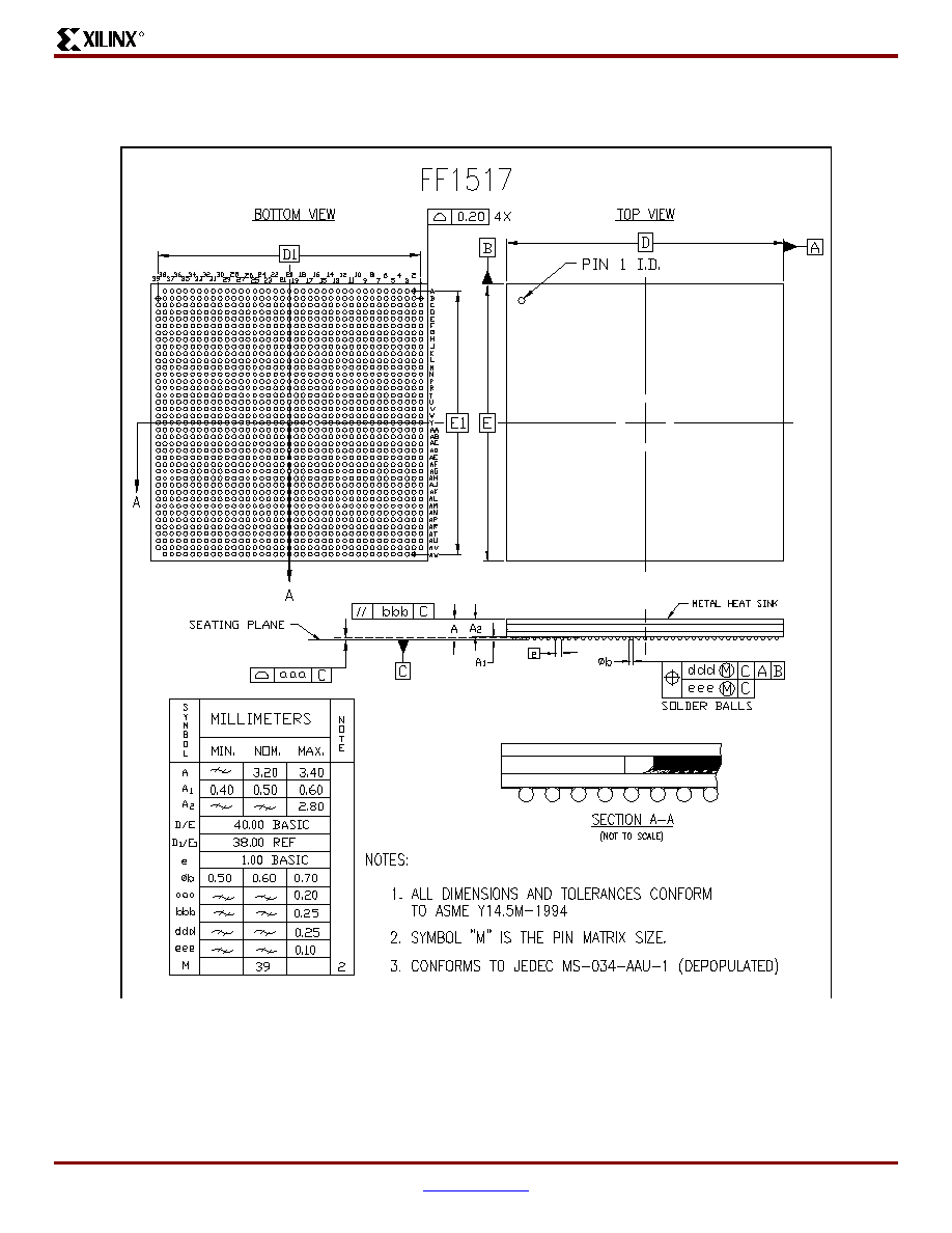
Virtex-II ProTM Platform FPGAs: Pinout Information
R
DS083-4 (v2.5.5) August 25, 2003
www.xilinx.com
201
Advance Product Specification
1-800-255-7778
FF1517 Flip-Chip Fine-Pitch BGA Package Specifications (1.00mm pitch)
Figure 8: FF1517 Flip-Chip Fine-Pitch BGA Package Specifications
FF1704 Flip-Chip Fine-Pitch BGA Package
R
202
www.xilinx.com
DS083-4 (v2.5.5) August 25, 2003
1-800-255-7778
Advance Product Specification
FF1704 Flip-Chip Fine-Pitch BGA Package
As shown in
Table 13
, XC2VP70, XC2VP100, and XC2VP125 Virtex-II Pro devices are available in the FF1704 flip-chip
fine-pitch BGA package. Following this table are the
FF1704 Flip-Chip Fine-Pitch BGA Package Specifications (1.00mm
pitch)
.
Table 13: FF1704 -- XC2VP70, XC2VP100, and XC2VP125
Bank
Pin Description
Pin Number
No Connects
XC2VP70
XC2VP100
XC2VP125
0
IO_L01N_0/VRP_0
G34
0
IO_L01P_0/VRN_0
H34
0
IO_L02N_0
F34
0
IO_L02P_0
E34
0
IO_L03N_0
C34
0
IO_L03P_0/VREF_0
D34
0
IO_L05_0/No_Pair
K32
0
IO_L06N_0
H33
0
IO_L06P_0
J33
0
IO_L07N_0
F33
0
IO_L07P_0
G33
0
IO_L08N_0
E33
0
IO_L08P_0
D33
0
IO_L09N_0
H32
0
IO_L09P_0/VREF_0
J32
0
IO_L19N_0
E32
0
IO_L19P_0
F32
0
IO_L20N_0
C33
0
IO_L20P_0
C32
0
IO_L21N_0
K31
0
IO_L21P_0
L31
0
IO_L25N_0
H31
0
IO_L25P_0
J31
0
IO_L26N_0
G31
0
IO_L26P_0
F31
0
IO_L27N_0
D31
0
IO_L27P_0/VREF_0
E31
0
IO_L28N_0
L30
0
IO_L28P_0
M30
0
IO_L29N_0
J30
0
IO_L29P_0
K30
0
IO_L30N_0
G30
0
IO_L30P_0
H30

Virtex-II ProTM Platform FPGAs: Pinout Information
R
DS083-4 (v2.5.5) August 25, 2003
www.xilinx.com
203
Advance Product Specification
1-800-255-7778
0
IO_L34N_0
E30
0
IO_L34P_0
F30
0
IO_L35N_0
D30
0
IO_L35P_0
C30
0
IO_L36N_0
M28
0
IO_L36P_0/VREF_0
M29
0
IO_L78N_0
K29
NC
0
IO_L78P_0
L29
NC
0
IO_L83_0/No_Pair
H29
NC
0
IO_L84N_0
F29
NC
0
IO_L84P_0
G29
NC
0
IO_L85N_0
D29
NC
0
IO_L85P_0
E29
NC
0
IO_L86N_0
L28
NC
0
IO_L86P_0
K28
NC
0
IO_L87N_0
H28
NC
0
IO_L87P_0/VREF_0
J28
NC
0
IO_L37N_0
E28
0
IO_L37P_0
F28
0
IO_L38N_0
C29
0
IO_L38P_0
C28
0
IO_L39N_0
L27
0
IO_L39P_0
M27
0
IO_L43N_0
J27
0
IO_L43P_0
K27
0
IO_L44N_0
H27
0
IO_L44P_0
G27
0
IO_L45N_0
E27
0
IO_L45P_0/VREF_0
F27
0
IO_L46N_0
M25
0
IO_L46P_0
M26
0
IO_L47N_0
L26
0
IO_L47P_0
K26
0
IO_L48N_0
H26
0
IO_L48P_0
J26
0
IO_L49N_0
F26
0
IO_L49P_0
G26
Table 13: FF1704 -- XC2VP70, XC2VP100, and XC2VP125
Bank
Pin Description
Pin Number
No Connects
XC2VP70
XC2VP100
XC2VP125

FF1704 Flip-Chip Fine-Pitch BGA Package
R
204
www.xilinx.com
DS083-4 (v2.5.5) August 25, 2003
1-800-255-7778
Advance Product Specification
0
IO_L50_0/No_Pair
D27
0
IO_L53_0/No_Pair
D26
0
IO_L54N_0
K25
0
IO_L54P_0
L25
0
IO_L55N_0
G25
0
IO_L55P_0
H25
0
IO_L56N_0
E26
0
IO_L56P_0
E25
0
IO_L57N_0
C25
0
IO_L57P_0/VREF_0
C26
0
IO_L58N_0
L24
0
IO_L58P_0
M24
0
IO_L59N_0
J24
0
IO_L59P_0
K24
0
IO_L60N_0
G24
0
IO_L60P_0
H24
0
IO_L64N_0
E24
0
IO_L64P_0
F24
0
IO_L65N_0
D24
0
IO_L65P_0
C24
0
IO_L66N_0
M22
0
IO_L66P_0/VREF_0
M23
0
IO_L67N_0
K23
0
IO_L67P_0
L23
0
IO_L68N_0
J23
0
IO_L68P_0
H23
0
IO_L69N_0
E23
0
IO_L69P_0/VREF_0
F23
0
IO_L73N_0
C23
0
IO_L73P_0
D23
0
IO_L74N_0/GCLK7P
K22
0
IO_L74P_0/GCLK6S
J22
0
IO_L75N_0/GCLK5P
F22
0
IO_L75P_0/GCLK4S
G22
1
IO_L75N_1/GCLK3P
G21
1
IO_L75P_1/GCLK2S
F21
Table 13: FF1704 -- XC2VP70, XC2VP100, and XC2VP125
Bank
Pin Description
Pin Number
No Connects
XC2VP70
XC2VP100
XC2VP125

Virtex-II ProTM Platform FPGAs: Pinout Information
R
DS083-4 (v2.5.5) August 25, 2003
www.xilinx.com
205
Advance Product Specification
1-800-255-7778
1
IO_L74N_1/GCLK1P
J21
1
IO_L74P_1/GCLK0S
K21
1
IO_L73N_1
D20
1
IO_L73P_1
C20
1
IO_L69N_1/VREF_1
F20
1
IO_L69P_1
E20
1
IO_L68N_1
H20
1
IO_L68P_1
J20
1
IO_L67N_1
L20
1
IO_L67P_1
K20
1
IO_L66N_1/VREF_1
M20
1
IO_L66P_1
M21
1
IO_L65N_1
C19
1
IO_L65P_1
D19
1
IO_L64N_1
F19
1
IO_L64P_1
E19
1
IO_L60N_1
H19
1
IO_L60P_1
G19
1
IO_L59N_1
K19
1
IO_L59P_1
J19
1
IO_L58N_1
M19
1
IO_L58P_1
L19
1
IO_L57N_1/VREF_1
C17
1
IO_L57P_1
C18
1
IO_L56N_1
E18
1
IO_L56P_1
E17
1
IO_L55N_1
H18
1
IO_L55P_1
G18
1
IO_L54N_1
L18
1
IO_L54P_1
K18
1
IO_L53_1/No_Pair
D17
1
IO_L50_1/No_Pair
D16
1
IO_L49N_1
G17
1
IO_L49P_1
F17
1
IO_L48N_1
J17
1
IO_L48P_1
H17
1
IO_L47N_1
K17
Table 13: FF1704 -- XC2VP70, XC2VP100, and XC2VP125
Bank
Pin Description
Pin Number
No Connects
XC2VP70
XC2VP100
XC2VP125
FF1704 Flip-Chip Fine-Pitch BGA Package
R
206
www.xilinx.com
DS083-4 (v2.5.5) August 25, 2003
1-800-255-7778
Advance Product Specification
1
IO_L47P_1
L17
1
IO_L46N_1
M17
1
IO_L46P_1
M18
1
IO_L45N_1/VREF_1
F16
1
IO_L45P_1
E16
1
IO_L44N_1
G16
1
IO_L44P_1
H16
1
IO_L43N_1
K16
1
IO_L43P_1
J16
1
IO_L39N_1
M16
1
IO_L39P_1
L16
1
IO_L38N_1
C15
1
IO_L38P_1
C14
1
IO_L37N_1
F15
1
IO_L37P_1
E15
1
IO_L87N_1/VREF_1
J15
NC
1
IO_L87P_1
H15
NC
1
IO_L86N_1
K15
NC
1
IO_L86P_1
L15
NC
1
IO_L85N_1
E14
NC
1
IO_L85P_1
D14
NC
1
IO_L84N_1
G14
NC
1
IO_L84P_1
F14
NC
1
IO_L83_1/No_Pair
H14
NC
1
IO_L78N_1
L14
NC
1
IO_L78P_1
K14
NC
1
IO_L36N_1/VREF_1
M14
1
IO_L36P_1
M15
1
IO_L35N_1
C13
1
IO_L35P_1
D13
1
IO_L34N_1
F13
1
IO_L34P_1
E13
1
IO_L30N_1
H13
1
IO_L30P_1
G13
1
IO_L29N_1
K13
1
IO_L29P_1
J13
1
IO_L28N_1
M13
Table 13: FF1704 -- XC2VP70, XC2VP100, and XC2VP125
Bank
Pin Description
Pin Number
No Connects
XC2VP70
XC2VP100
XC2VP125

Virtex-II ProTM Platform FPGAs: Pinout Information
R
DS083-4 (v2.5.5) August 25, 2003
www.xilinx.com
207
Advance Product Specification
1-800-255-7778
1
IO_L28P_1
L13
1
IO_L27N_1/VREF_1
E12
1
IO_L27P_1
D12
1
IO_L26N_1
F12
1
IO_L26P_1
G12
1
IO_L25N_1
J12
1
IO_L25P_1
H12
1
IO_L21N_1
L12
1
IO_L21P_1
K12
1
IO_L20N_1
C11
1
IO_L20P_1
C10
1
IO_L19N_1
F11
1
IO_L19P_1
E11
1
IO_L09N_1/VREF_1
J11
1
IO_L09P_1
H11
1
IO_L08N_1
D10
1
IO_L08P_1
E10
1
IO_L07N_1
G10
1
IO_L07P_1
F10
1
IO_L06N_1
J10
1
IO_L06P_1
H10
1
IO_L05_1/No_Pair
K11
1
IO_L03N_1/VREF_1
D9
1
IO_L03P_1
C9
1
IO_L02N_1
E9
1
IO_L02P_1
F9
1
IO_L01N_1/VRP_1
H9
1
IO_L01P_1/VRN_1
G9
2
IO_L01N_2/VRP_2
C5
2
IO_L01P_2/VRN_2
C6
2
IO_L02N_2
E7
2
IO_L02P_2
D7
2
IO_L03N_2
E6
2
IO_L03P_2
D6
2
IO_L04N_2/VREF_2
G6
2
IO_L04P_2
F7
Table 13: FF1704 -- XC2VP70, XC2VP100, and XC2VP125
Bank
Pin Description
Pin Number
No Connects
XC2VP70
XC2VP100
XC2VP125

FF1704 Flip-Chip Fine-Pitch BGA Package
R
208
www.xilinx.com
DS083-4 (v2.5.5) August 25, 2003
1-800-255-7778
Advance Product Specification
2
IO_L05N_2
D3
2
IO_L05P_2
E3
2
IO_L06N_2
D1
2
IO_L06P_2
D2
2
IO_L73N_2
E1
2
IO_L73P_2
E2
2
IO_L74N_2
F4
2
IO_L74P_2
F3
2
IO_L75N_2
F1
2
IO_L75P_2
F2
2
IO_L76N_2/VREF_2
G3
2
IO_L76P_2
G4
2
IO_L77N_2
G2
2
IO_L77P_2
G1
2
IO_L78N_2
G5
2
IO_L78P_2
H6
2
IO_L79N_2
H4
2
IO_L79P_2
H5
2
IO_L80N_2
H3
2
IO_L80P_2
H2
2
IO_L81N_2
H7
2
IO_L81P_2
J8
2
IO_L82N_2/VREF_2
J6
2
IO_L82P_2
J7
2
IO_L83N_2
J5
2
IO_L83P_2
J4
2
IO_L84N_2
J1
2
IO_L84P_2
J2
2
IO_L07N_2
K9
2
IO_L07P_2
L10
2
IO_L08N_2
K6
2
IO_L08P_2
K5
2
IO_L09N_2
K8
2
IO_L09P_2
K7
2
IO_L10N_2/VREF_2
K2
2
IO_L10P_2
K1
2
IO_L11N_2
L8
Table 13: FF1704 -- XC2VP70, XC2VP100, and XC2VP125
Bank
Pin Description
Pin Number
No Connects
XC2VP70
XC2VP100
XC2VP125

Virtex-II ProTM Platform FPGAs: Pinout Information
R
DS083-4 (v2.5.5) August 25, 2003
www.xilinx.com
209
Advance Product Specification
1-800-255-7778
2
IO_L11P_2
L9
2
IO_L12N_2
L6
2
IO_L12P_2
L7
2
IO_L13N_2
K3
2
IO_L13P_2
L3
2
IO_L14N_2
L5
2
IO_L14P_2
L4
2
IO_L15N_2
L1
2
IO_L15P_2
L2
2
IO_L16N_2/VREF_2
M7
2
IO_L16P_2
M8
2
IO_L17N_2
M11
2
IO_L17P_2
M12
2
IO_L18N_2
M9
2
IO_L18P_2
M10
2
IO_L19N_2
M2
2
IO_L19P_2
M3
2
IO_L20N_2
M4
2
IO_L20P_2
M5
2
IO_L21N_2
N7
2
IO_L21P_2
N8
2
IO_L22N_2/VREF_2
N5
2
IO_L22P_2
N6
2
IO_L23N_2
N9
2
IO_L23P_2
N10
2
IO_L24N_2
N3
2
IO_L24P_2
N4
2
IO_L25N_2
N1
2
IO_L25P_2
N2
2
IO_L26N_2
N11
2
IO_L26P_2
N12
2
IO_L27N_2
P9
2
IO_L27P_2
P10
2
IO_L28N_2/VREF_2
P7
2
IO_L28P_2
P8
2
IO_L29N_2
P11
2
IO_L29P_2
P12
Table 13: FF1704 -- XC2VP70, XC2VP100, and XC2VP125
Bank
Pin Description
Pin Number
No Connects
XC2VP70
XC2VP100
XC2VP125

FF1704 Flip-Chip Fine-Pitch BGA Package
R
210
www.xilinx.com
DS083-4 (v2.5.5) August 25, 2003
1-800-255-7778
Advance Product Specification
2
IO_L30N_2
P5
2
IO_L30P_2
P6
2
IO_L31N_2
P1
2
IO_L31P_2
P2
2
IO_L32N_2
R9
2
IO_L32P_2
R10
2
IO_L33N_2
R5
2
IO_L33P_2
R6
2
IO_L34N_2/VREF_2
P3
2
IO_L34P_2
R3
2
IO_L35N_2
R1
2
IO_L35P_2
R2
2
IO_L36N_2
R11
2
IO_L36P_2
R12
2
IO_L37N_2
T6
2
IO_L37P_2
T7
2
IO_L38N_2
T8
2
IO_L38P_2
R8
2
IO_L39N_2
T4
2
IO_L39P_2
T5
2
IO_L40N_2/VREF_2
T2
2
IO_L40P_2
T3
2
IO_L41N_2
T10
2
IO_L41P_2
T11
2
IO_L42N_2
U7
2
IO_L42P_2
U8
2
IO_L43N_2
U5
2
IO_L43P_2
U6
2
IO_L44N_2
U9
2
IO_L44P_2
U10
2
IO_L45N_2
U3
2
IO_L45P_2
U4
2
IO_L46N_2/VREF_2
U1
2
IO_L46P_2
U2
2
IO_L47N_2
T12
2
IO_L47P_2
U12
2
IO_L48N_2
V10
Table 13: FF1704 -- XC2VP70, XC2VP100, and XC2VP125
Bank
Pin Description
Pin Number
No Connects
XC2VP70
XC2VP100
XC2VP125

Virtex-II ProTM Platform FPGAs: Pinout Information
R
DS083-4 (v2.5.5) August 25, 2003
www.xilinx.com
211
Advance Product Specification
1-800-255-7778
2
IO_L48P_2
V11
2
IO_L49N_2
V7
2
IO_L49P_2
V8
2
IO_L50N_2
U11
2
IO_L50P_2
V12
2
IO_L51N_2
V4
2
IO_L51P_2
V5
2
IO_L52N_2/VREF_2
V1
2
IO_L52P_2
V2
2
IO_L53N_2
W9
2
IO_L53P_2
W10
2
IO_L54N_2
W7
2
IO_L54P_2
W8
2
IO_L55N_2
W5
2
IO_L55P_2
W6
2
IO_L56N_2
W11
2
IO_L56P_2
W12
2
IO_L57N_2
W3
2
IO_L57P_2
W4
2
IO_L58N_2/VREF_2
W1
2
IO_L58P_2
W2
2
IO_L59N_2
Y9
2
IO_L59P_2
Y10
2
IO_L60N_2
Y6
2
IO_L60P_2
Y7
2
IO_L85N_2
Y3
2
IO_L85P_2
Y4
2
IO_L86N_2
Y11
2
IO_L86P_2
Y12
2
IO_L87N_2
AA9
2
IO_L87P_2
AA10
2
IO_L88N_2/VREF_2
AA6
2
IO_L88P_2
AA7
2
IO_L89N_2
AA12
2
IO_L89P_2
AB12
2
IO_L90N_2
AA3
2
IO_L90P_2
AA4
Table 13: FF1704 -- XC2VP70, XC2VP100, and XC2VP125
Bank
Pin Description
Pin Number
No Connects
XC2VP70
XC2VP100
XC2VP125
FF1704 Flip-Chip Fine-Pitch BGA Package
R
212
www.xilinx.com
DS083-4 (v2.5.5) August 25, 2003
1-800-255-7778
Advance Product Specification
3
IO_L90N_3
AB3
3
IO_L90P_3
AB4
3
IO_L89N_3
AB6
3
IO_L89P_3
AB7
3
IO_L88N_3
AB9
3
IO_L88P_3
AB10
3
IO_L87N_3/VREF_3
AC3
3
IO_L87P_3
AC4
3
IO_L86N_3
AC11
3
IO_L86P_3
AC12
3
IO_L85N_3
AC6
3
IO_L85P_3
AC7
3
IO_L60N_3
AC9
3
IO_L60P_3
AC10
3
IO_L59N_3
AD9
3
IO_L59P_3
AD10
3
IO_L58N_3
AD1
3
IO_L58P_3
AD2
3
IO_L57N_3/VREF_3
AD3
3
IO_L57P_3
AD4
3
IO_L56N_3
AD11
3
IO_L56P_3
AD12
3
IO_L55N_3
AD5
3
IO_L55P_3
AD6
3
IO_L54N_3
AD7
3
IO_L54P_3
AD8
3
IO_L53N_3
AE10
3
IO_L53P_3
AE11
3
IO_L52N_3
AE1
3
IO_L52P_3
AE2
3
IO_L51N_3/VREF_3
AE4
3
IO_L51P_3
AE5
3
IO_L50N_3
AF11
3
IO_L50P_3
AE12
3
IO_L49N_3
AE7
3
IO_L49P_3
AE8
Table 13: FF1704 -- XC2VP70, XC2VP100, and XC2VP125
Bank
Pin Description
Pin Number
No Connects
XC2VP70
XC2VP100
XC2VP125

Virtex-II ProTM Platform FPGAs: Pinout Information
R
DS083-4 (v2.5.5) August 25, 2003
www.xilinx.com
213
Advance Product Specification
1-800-255-7778
3
IO_L48N_3
AF1
3
IO_L48P_3
AF2
3
IO_L47N_3
AG12
3
IO_L47P_3
AF12
3
IO_L46N_3
AF3
3
IO_L46P_3
AF4
3
IO_L45N_3/VREF_3
AF5
3
IO_L45P_3
AF6
3
IO_L44N_3
AF7
3
IO_L44P_3
AF8
3
IO_L43N_3
AF9
3
IO_L43P_3
AF10
3
IO_L42N_3
AG2
3
IO_L42P_3
AG3
3
IO_L41N_3
AG10
3
IO_L41P_3
AG11
3
IO_L40N_3
AG4
3
IO_L40P_3
AG5
3
IO_L39N_3/VREF_3
AG6
3
IO_L39P_3
AG7
3
IO_L38N_3
AG8
3
IO_L38P_3
AH8
3
IO_L37N_3
AH1
3
IO_L37P_3
AH2
3
IO_L36N_3
AH3
3
IO_L36P_3
AJ3
3
IO_L35N_3
AH11
3
IO_L35P_3
AH12
3
IO_L34N_3
AH5
3
IO_L34P_3
AH6
3
IO_L33N_3/VREF_3
AH9
3
IO_L33P_3
AH10
3
IO_L32N_3
AJ11
3
IO_L32P_3
AJ12
3
IO_L31N_3
AJ1
3
IO_L31P_3
AJ2
3
IO_L30N_3
AJ5
Table 13: FF1704 -- XC2VP70, XC2VP100, and XC2VP125
Bank
Pin Description
Pin Number
No Connects
XC2VP70
XC2VP100
XC2VP125

FF1704 Flip-Chip Fine-Pitch BGA Package
R
214
www.xilinx.com
DS083-4 (v2.5.5) August 25, 2003
1-800-255-7778
Advance Product Specification
3
IO_L30P_3
AJ6
3
IO_L29N_3
AJ9
3
IO_L29P_3
AJ10
3
IO_L28N_3
AJ7
3
IO_L28P_3
AJ8
3
IO_L27N_3/VREF_3
AK1
3
IO_L27P_3
AK2
3
IO_L26N_3
AK11
3
IO_L26P_3
AK12
3
IO_L25N_3
AK3
3
IO_L25P_3
AK4
3
IO_L24N_3
AK5
3
IO_L24P_3
AK6
3
IO_L23N_3
AK9
3
IO_L23P_3
AK10
3
IO_L22N_3
AK7
3
IO_L22P_3
AK8
3
IO_L21N_3/VREF_3
AL2
3
IO_L21P_3
AL3
3
IO_L20N_3
AL11
3
IO_L20P_3
AL12
3
IO_L19N_3
AL4
3
IO_L19P_3
AL5
3
IO_L18N_3
AL7
3
IO_L18P_3
AL8
3
IO_L17N_3
AL9
3
IO_L17P_3
AL10
3
IO_L16N_3
AM1
3
IO_L16P_3
AM2
3
IO_L15N_3/VREF_3
AM3
3
IO_L15P_3
AN3
3
IO_L14N_3
AM8
3
IO_L14P_3
AM9
3
IO_L13N_3
AM4
3
IO_L13P_3
AM5
3
IO_L12N_3
AM6
3
IO_L12P_3
AM7
Table 13: FF1704 -- XC2VP70, XC2VP100, and XC2VP125
Bank
Pin Description
Pin Number
No Connects
XC2VP70
XC2VP100
XC2VP125

Virtex-II ProTM Platform FPGAs: Pinout Information
R
DS083-4 (v2.5.5) August 25, 2003
www.xilinx.com
215
Advance Product Specification
1-800-255-7778
3
IO_L11N_3
AN9
3
IO_L11P_3
AM10
3
IO_L10N_3
AN1
3
IO_L10P_3
AN2
3
IO_L09N_3/VREF_3
AN5
3
IO_L09P_3
AN6
3
IO_L08N_3
AN7
3
IO_L08P_3
AN8
3
IO_L07N_3
AP1
3
IO_L07P_3
AP2
3
IO_L84N_3
AP4
3
IO_L84P_3
AP5
3
IO_L83N_3
AR7
3
IO_L83P_3
AP8
3
IO_L82N_3
AP6
3
IO_L82P_3
AP7
3
IO_L81N_3/VREF_3
AR2
3
IO_L81P_3
AR3
3
IO_L80N_3
AT5
3
IO_L80P_3
AR6
3
IO_L79N_3
AR4
3
IO_L79P_3
AR5
3
IO_L78N_3
AT1
3
IO_L78P_3
AT2
3
IO_L77N_3
AT3
3
IO_L77P_3
AT4
3
IO_L76N_3
AU1
3
IO_L76P_3
AU2
3
IO_L75N_3/VREF_3
AU3
3
IO_L75P_3
AU4
3
IO_L74N_3
AV3
3
IO_L74P_3
AW3
3
IO_L73N_3
AV1
3
IO_L73P_3
AV2
3
IO_L06N_3
AW1
3
IO_L06P_3
AW2
3
IO_L05N_3
AT8
Table 13: FF1704 -- XC2VP70, XC2VP100, and XC2VP125
Bank
Pin Description
Pin Number
No Connects
XC2VP70
XC2VP100
XC2VP125
FF1704 Flip-Chip Fine-Pitch BGA Package
R
216
www.xilinx.com
DS083-4 (v2.5.5) August 25, 2003
1-800-255-7778
Advance Product Specification
3
IO_L05P_3
AU8
3
IO_L04N_3
AT6
3
IO_L04P_3
AU7
3
IO_L03N_3/VREF_3
AY5
3
IO_L03P_3
AY6
3
IO_L02N_3
AV7
3
IO_L02P_3
AW7
3
IO_L01N_3/VRP_3
AV6
3
IO_L01P_3/VRN_3
AW6
4
IO_L01N_4/BUSY/DOUT
(1)
AT9
4
IO_L01P_4/INIT_B
AR9
4
IO_L02N_4/D0/DIN
(1)
AU9
4
IO_L02P_4/D1
AV9
4
IO_L03N_4/D2
AY9
4
IO_L03P_4/D3
AW9
4
IO_L05_4/No_Pair
AN11
4
IO_L06N_4/VRP_4
AR10
4
IO_L06P_4/VRN_4
AP10
4
IO_L07N_4
AU10
4
IO_L07P_4/VREF_4
AT10
4
IO_L08N_4
AV10
4
IO_L08P_4
AW10
4
IO_L09N_4
AR11
4
IO_L09P_4/VREF_4
AP11
4
IO_L19N_4
AV11
4
IO_L19P_4
AU11
4
IO_L20N_4
AY10
4
IO_L20P_4
AY11
4
IO_L21N_4
AN12
4
IO_L21P_4
AM12
4
IO_L25N_4
AR12
4
IO_L25P_4
AP12
4
IO_L26N_4
AT12
4
IO_L26P_4
AU12
4
IO_L27N_4
AW12
4
IO_L27P_4/VREF_4
AV12
Table 13: FF1704 -- XC2VP70, XC2VP100, and XC2VP125
Bank
Pin Description
Pin Number
No Connects
XC2VP70
XC2VP100
XC2VP125
Virtex-II ProTM Platform FPGAs: Pinout Information
R
DS083-4 (v2.5.5) August 25, 2003
www.xilinx.com
217
Advance Product Specification
1-800-255-7778
4
IO_L28N_4
AM13
4
IO_L28P_4
AL13
4
IO_L29N_4
AP13
4
IO_L29P_4
AN13
4
IO_L30N_4
AT13
4
IO_L30P_4
AR13
4
IO_L34N_4
AV13
4
IO_L34P_4
AU13
4
IO_L35N_4
AW13
4
IO_L35P_4
AY13
4
IO_L36N_4
AL15
4
IO_L36P_4/VREF_4
AL14
4
IO_L78N_4
AN14
NC
4
IO_L78P_4
AM14
NC
4
IO_L83_4/No_Pair
AR14
NC
4
IO_L84N_4
AU14
NC
4
IO_L84P_4
AT14
NC
4
IO_L85N_4
AW14
NC
4
IO_L85P_4
AV14
NC
4
IO_L86N_4
AM15
NC
4
IO_L86P_4
AN15
NC
4
IO_L87N_4
AR15
NC
4
IO_L87P_4/VREF_4
AP15
NC
4
IO_L37N_4
AV15
4
IO_L37P_4
AU15
4
IO_L38N_4
AY14
4
IO_L38P_4
AY15
4
IO_L39N_4
AM16
4
IO_L39P_4
AL16
4
IO_L43N_4
AP16
4
IO_L43P_4
AN16
4
IO_L44N_4
AR16
4
IO_L44P_4
AT16
4
IO_L45N_4
AV16
4
IO_L45P_4/VREF_4
AU16
4
IO_L46N_4
AL18
4
IO_L46P_4
AL17
Table 13: FF1704 -- XC2VP70, XC2VP100, and XC2VP125
Bank
Pin Description
Pin Number
No Connects
XC2VP70
XC2VP100
XC2VP125

FF1704 Flip-Chip Fine-Pitch BGA Package
R
218
www.xilinx.com
DS083-4 (v2.5.5) August 25, 2003
1-800-255-7778
Advance Product Specification
4
IO_L47N_4
AM17
4
IO_L47P_4
AN17
4
IO_L48N_4
AR17
4
IO_L48P_4
AP17
4
IO_L49N_4
AU17
4
IO_L49P_4
AT17
4
IO_L50_4/No_Pair
AW16
4
IO_L53_4/No_Pair
AW17
4
IO_L54N_4
AN18
4
IO_L54P_4
AM18
4
IO_L55N_4
AT18
4
IO_L55P_4
AR18
4
IO_L56N_4
AV17
4
IO_L56P_4
AV18
4
IO_L57N_4
AY18
4
IO_L57P_4/VREF_4
AY17
4
IO_L58N_4
AM19
4
IO_L58P_4
AL19
4
IO_L59N_4
AP19
4
IO_L59P_4
AN19
4
IO_L60N_4
AT19
4
IO_L60P_4
AR19
4
IO_L64N_4
AV19
4
IO_L64P_4
AU19
4
IO_L65N_4
AW19
4
IO_L65P_4
AY19
4
IO_L66N_4
AL21
4
IO_L66P_4/VREF_4
AL20
4
IO_L67N_4
AN20
4
IO_L67P_4
AM20
4
IO_L68N_4
AP20
4
IO_L68P_4
AR20
4
IO_L69N_4
AV20
4
IO_L69P_4/VREF_4
AU20
4
IO_L73N_4
AY20
4
IO_L73P_4
AW20
4
IO_L74N_4/GCLK3S
AN21
Table 13: FF1704 -- XC2VP70, XC2VP100, and XC2VP125
Bank
Pin Description
Pin Number
No Connects
XC2VP70
XC2VP100
XC2VP125
Virtex-II ProTM Platform FPGAs: Pinout Information
R
DS083-4 (v2.5.5) August 25, 2003
www.xilinx.com
219
Advance Product Specification
1-800-255-7778
4
IO_L74P_4/GCLK2P
AP21
4
IO_L75N_4/GCLK1S
AU21
4
IO_L75P_4/GCLK0P
AT21
5
IO_L75N_5/GCLK7S
AT22
5
IO_L75P_5/GCLK6P
AU22
5
IO_L74N_5/GCLK5S
AP22
5
IO_L74P_5/GCLK4P
AN22
5
IO_L73N_5
AW23
5
IO_L73P_5
AY23
5
IO_L69N_5/VREF_5
AU23
5
IO_L69P_5
AV23
5
IO_L68N_5
AR23
5
IO_L68P_5
AP23
5
IO_L67N_5
AM23
5
IO_L67P_5
AN23
5
IO_L66N_5/VREF_5
AL23
5
IO_L66P_5
AL22
5
IO_L65N_5
AY24
5
IO_L65P_5
AW24
5
IO_L64N_5
AU24
5
IO_L64P_5
AV24
5
IO_L60N_5
AR24
5
IO_L60P_5
AT24
5
IO_L59N_5
AN24
5
IO_L59P_5
AP24
5
IO_L58N_5
AL24
5
IO_L58P_5
AM24
5
IO_L57N_5/VREF_5
AY26
5
IO_L57P_5
AY25
5
IO_L56N_5
AV25
5
IO_L56P_5
AV26
5
IO_L55N_5
AR25
5
IO_L55P_5
AT25
5
IO_L54N_5
AM25
5
IO_L54P_5
AN25
5
IO_L53_5/No_Pair
AW26
Table 13: FF1704 -- XC2VP70, XC2VP100, and XC2VP125
Bank
Pin Description
Pin Number
No Connects
XC2VP70
XC2VP100
XC2VP125
FF1704 Flip-Chip Fine-Pitch BGA Package
R
220
www.xilinx.com
DS083-4 (v2.5.5) August 25, 2003
1-800-255-7778
Advance Product Specification
5
IO_L50_5/No_Pair
AW27
5
IO_L49N_5
AT26
5
IO_L49P_5
AU26
5
IO_L48N_5
AP26
5
IO_L48P_5
AR26
5
IO_L47N_5
AN26
5
IO_L47P_5
AM26
5
IO_L46N_5
AL26
5
IO_L46P_5
AL25
5
IO_L45N_5/VREF_5
AU27
5
IO_L45P_5
AV27
5
IO_L44N_5
AT27
5
IO_L44P_5
AR27
5
IO_L43N_5
AN27
5
IO_L43P_5
AP27
5
IO_L39N_5
AL27
5
IO_L39P_5
AM27
5
IO_L38N_5
AY28
5
IO_L38P_5
AY29
5
IO_L37N_5
AU28
5
IO_L37P_5
AV28
5
IO_L87N_5/VREF_5
AP28
NC
5
IO_L87P_5
AR28
NC
5
IO_L86N_5
AN28
NC
5
IO_L86P_5
AM28
NC
5
IO_L85N_5
AV29
NC
5
IO_L85P_5
AW29
NC
5
IO_L84N_5
AT29
NC
5
IO_L84P_5
AU29
NC
5
IO_L83_5/No_Pair
AR29
NC
5
IO_L78N_5
AM29
NC
5
IO_L78P_5
AN29
NC
5
IO_L36N_5/VREF_5
AL29
5
IO_L36P_5
AL28
5
IO_L35N_5
AY30
5
IO_L35P_5
AW30
5
IO_L34N_5
AU30
Table 13: FF1704 -- XC2VP70, XC2VP100, and XC2VP125
Bank
Pin Description
Pin Number
No Connects
XC2VP70
XC2VP100
XC2VP125
Virtex-II ProTM Platform FPGAs: Pinout Information
R
DS083-4 (v2.5.5) August 25, 2003
www.xilinx.com
221
Advance Product Specification
1-800-255-7778
5
IO_L34P_5
AV30
5
IO_L30N_5
AR30
5
IO_L30P_5
AT30
5
IO_L29N_5
AN30
5
IO_L29P_5
AP30
5
IO_L28N_5
AL30
5
IO_L28P_5
AM30
5
IO_L27N_5/VREF_5
AV31
5
IO_L27P_5
AW31
5
IO_L26N_5
AU31
5
IO_L26P_5
AT31
5
IO_L25N_5
AP31
5
IO_L25P_5
AR31
5
IO_L21N_5
AM31
5
IO_L21P_5
AN31
5
IO_L20N_5
AY32
5
IO_L20P_5
AY33
5
IO_L19N_5
AU32
5
IO_L19P_5
AV32
5
IO_L09N_5/VREF_5
AP32
5
IO_L09P_5
AR32
5
IO_L08N_5
AW33
5
IO_L08P_5
AV33
5
IO_L07N_5/VREF_5
AT33
5
IO_L07P_5
AU33
5
IO_L06N_5/VRP_5
AP33
5
IO_L06P_5/VRN_5
AR33
5
IO_L05_5/No_Pair
AN32
5
IO_L03N_5/D4
AW34
5
IO_L03P_5/D5
AY34
5
IO_L02N_5/D6
AV34
5
IO_L02P_5/D7
AU34
5
IO_L01N_5/RDWR_B
AR34
5
IO_L01P_5/CS_B
AT34
6
IO_L01P_6/VRN_6
AW37
6
IO_L01N_6/VRP_6
AV37
Table 13: FF1704 -- XC2VP70, XC2VP100, and XC2VP125
Bank
Pin Description
Pin Number
No Connects
XC2VP70
XC2VP100
XC2VP125

FF1704 Flip-Chip Fine-Pitch BGA Package
R
222
www.xilinx.com
DS083-4 (v2.5.5) August 25, 2003
1-800-255-7778
Advance Product Specification
6
IO_L02P_6
AW36
6
IO_L02N_6
AV36
6
IO_L03P_6
AY37
6
IO_L03N_6/VREF_6
AY38
6
IO_L04P_6
AU36
6
IO_L04N_6
AT37
6
IO_L05P_6
AU35
6
IO_L05N_6
AT35
6
IO_L06P_6
AW41
6
IO_L06N_6
AW42
6
IO_L73P_6
AV41
6
IO_L73N_6
AV42
6
IO_L74P_6
AW40
6
IO_L74N_6
AV40
6
IO_L75P_6
AU39
6
IO_L75N_6/VREF_6
AU40
6
IO_L76P_6
AU41
6
IO_L76N_6
AU42
6
IO_L77P_6
AT39
6
IO_L77N_6
AT40
6
IO_L78P_6
AT41
6
IO_L78N_6
AT42
6
IO_L79P_6
AR38
6
IO_L79N_6
AR39
6
IO_L80P_6
AR37
6
IO_L80N_6
AT38
6
IO_L81P_6
AR40
6
IO_L81N_6/VREF_6
AR41
6
IO_L82P_6
AP36
6
IO_L82N_6
AP37
6
IO_L83P_6
AP35
6
IO_L83N_6
AR36
6
IO_L84P_6
AP38
6
IO_L84N_6
AP39
6
IO_L07P_6
AP41
6
IO_L07N_6
AP42
6
IO_L08P_6
AN35
Table 13: FF1704 -- XC2VP70, XC2VP100, and XC2VP125
Bank
Pin Description
Pin Number
No Connects
XC2VP70
XC2VP100
XC2VP125

Virtex-II ProTM Platform FPGAs: Pinout Information
R
DS083-4 (v2.5.5) August 25, 2003
www.xilinx.com
223
Advance Product Specification
1-800-255-7778
6
IO_L08N_6
AN36
6
IO_L09P_6
AN37
6
IO_L09N_6/VREF_6
AN38
6
IO_L10P_6
AN41
6
IO_L10N_6
AN42
6
IO_L11P_6
AM33
6
IO_L11N_6
AN34
6
IO_L12P_6
AM36
6
IO_L12N_6
AM37
6
IO_L13P_6
AM38
6
IO_L13N_6
AM39
6
IO_L14P_6
AM34
6
IO_L14N_6
AM35
6
IO_L15P_6
AN40
6
IO_L15N_6/VREF_6
AM40
6
IO_L16P_6
AM41
6
IO_L16N_6
AM42
6
IO_L17P_6
AL33
6
IO_L17N_6
AL34
6
IO_L18P_6
AL35
6
IO_L18N_6
AL36
6
IO_L19P_6
AL38
6
IO_L19N_6
AL39
6
IO_L20P_6
AL31
6
IO_L20N_6
AL32
6
IO_L21P_6
AL40
6
IO_L21N_6/VREF_6
AL41
6
IO_L22P_6
AK35
6
IO_L22N_6
AK36
6
IO_L23P_6
AK33
6
IO_L23N_6
AK34
6
IO_L24P_6
AK37
6
IO_L24N_6
AK38
6
IO_L25P_6
AK39
6
IO_L25N_6
AK40
6
IO_L26P_6
AK31
6
IO_L26N_6
AK32
Table 13: FF1704 -- XC2VP70, XC2VP100, and XC2VP125
Bank
Pin Description
Pin Number
No Connects
XC2VP70
XC2VP100
XC2VP125

FF1704 Flip-Chip Fine-Pitch BGA Package
R
224
www.xilinx.com
DS083-4 (v2.5.5) August 25, 2003
1-800-255-7778
Advance Product Specification
6
IO_L27P_6
AK41
6
IO_L27N_6/VREF_6
AK42
6
IO_L28P_6
AJ35
6
IO_L28N_6
AJ36
6
IO_L29P_6
AJ33
6
IO_L29N_6
AJ34
6
IO_L30P_6
AJ37
6
IO_L30N_6
AJ38
6
IO_L31P_6
AJ41
6
IO_L31N_6
AJ42
6
IO_L32P_6
AJ31
6
IO_L32N_6
AJ32
6
IO_L33P_6
AH33
6
IO_L33N_6/VREF_6
AH34
6
IO_L34P_6
AH37
6
IO_L34N_6
AH38
6
IO_L35P_6
AH31
6
IO_L35N_6
AH32
6
IO_L36P_6
AJ40
6
IO_L36N_6
AH40
6
IO_L37P_6
AH41
6
IO_L37N_6
AH42
6
IO_L38P_6
AH35
6
IO_L38N_6
AG35
6
IO_L39P_6
AG36
6
IO_L39N_6/VREF_6
AG37
6
IO_L40P_6
AG38
6
IO_L40N_6
AG39
6
IO_L41P_6
AG32
6
IO_L41N_6
AG33
6
IO_L42P_6
AG40
6
IO_L42N_6
AG41
6
IO_L43P_6
AF33
6
IO_L43N_6
AF34
6
IO_L44P_6
AF35
6
IO_L44N_6
AF36
6
IO_L45P_6
AF37
Table 13: FF1704 -- XC2VP70, XC2VP100, and XC2VP125
Bank
Pin Description
Pin Number
No Connects
XC2VP70
XC2VP100
XC2VP125

Virtex-II ProTM Platform FPGAs: Pinout Information
R
DS083-4 (v2.5.5) August 25, 2003
www.xilinx.com
225
Advance Product Specification
1-800-255-7778
6
IO_L45N_6/VREF_6
AF38
6
IO_L46P_6
AF39
6
IO_L46N_6
AF40
6
IO_L47P_6
AF31
6
IO_L47N_6
AG31
6
IO_L48P_6
AF41
6
IO_L48N_6
AF42
6
IO_L49P_6
AE35
6
IO_L49N_6
AE36
6
IO_L50P_6
AE31
6
IO_L50N_6
AF32
6
IO_L51P_6
AE38
6
IO_L51N_6/VREF_6
AE39
6
IO_L52P_6
AE41
6
IO_L52N_6
AE42
6
IO_L53P_6
AE32
6
IO_L53N_6
AE33
6
IO_L54P_6
AD35
6
IO_L54N_6
AD36
6
IO_L55P_6
AD37
6
IO_L55N_6
AD38
6
IO_L56P_6
AD31
6
IO_L56N_6
AD32
6
IO_L57P_6
AD39
6
IO_L57N_6/VREF_6
AD40
6
IO_L58P_6
AD41
6
IO_L58N_6
AD42
6
IO_L59P_6
AD33
6
IO_L59N_6
AD34
6
IO_L60P_6
AC33
6
IO_L60N_6
AC34
6
IO_L85P_6
AC36
6
IO_L85N_6
AC37
6
IO_L86P_6
AC31
6
IO_L86N_6
AC32
6
IO_L87P_6
AC39
6
IO_L87N_6/VREF_6
AC40
Table 13: FF1704 -- XC2VP70, XC2VP100, and XC2VP125
Bank
Pin Description
Pin Number
No Connects
XC2VP70
XC2VP100
XC2VP125
FF1704 Flip-Chip Fine-Pitch BGA Package
R
226
www.xilinx.com
DS083-4 (v2.5.5) August 25, 2003
1-800-255-7778
Advance Product Specification
6
IO_L88P_6
AB33
6
IO_L88N_6
AB34
6
IO_L89P_6
AB36
6
IO_L89N_6
AB37
6
IO_L90P_6
AB39
6
IO_L90N_6
AB40
7
IO_L90P_7
AA39
7
IO_L90N_7
AA40
7
IO_L89P_7
AB31
7
IO_L89N_7
AA31
7
IO_L88P_7
AA36
7
IO_L88N_7/VREF_7
AA37
7
IO_L87P_7
AA33
7
IO_L87N_7
AA34
7
IO_L86P_7
Y31
7
IO_L86N_7
Y32
7
IO_L85P_7
Y39
7
IO_L85N_7
Y40
7
IO_L60P_7
Y36
7
IO_L60N_7
Y37
7
IO_L59P_7
Y33
7
IO_L59N_7
Y34
7
IO_L58P_7
W41
7
IO_L58N_7/VREF_7
W42
7
IO_L57P_7
W39
7
IO_L57N_7
W40
7
IO_L56P_7
W31
7
IO_L56N_7
W32
7
IO_L55P_7
W37
7
IO_L55N_7
W38
7
IO_L54P_7
W35
7
IO_L54N_7
W36
7
IO_L53P_7
W33
7
IO_L53N_7
W34
7
IO_L52P_7
V41
7
IO_L52N_7/VREF_7
V42
Table 13: FF1704 -- XC2VP70, XC2VP100, and XC2VP125
Bank
Pin Description
Pin Number
No Connects
XC2VP70
XC2VP100
XC2VP125

Virtex-II ProTM Platform FPGAs: Pinout Information
R
DS083-4 (v2.5.5) August 25, 2003
www.xilinx.com
227
Advance Product Specification
1-800-255-7778
7
IO_L51P_7
V38
7
IO_L51N_7
V39
7
IO_L50P_7
V31
7
IO_L50N_7
U32
7
IO_L49P_7
V35
7
IO_L49N_7
V36
7
IO_L48P_7
V32
7
IO_L48N_7
V33
7
IO_L47P_7
U31
7
IO_L47N_7
T31
7
IO_L46P_7
U41
7
IO_L46N_7/VREF_7
U42
7
IO_L45P_7
U39
7
IO_L45N_7
U40
7
IO_L44P_7
U33
7
IO_L44N_7
U34
7
IO_L43P_7
U37
7
IO_L43N_7
U38
7
IO_L42P_7
U35
7
IO_L42N_7
U36
7
IO_L41P_7
T32
7
IO_L41N_7
T33
7
IO_L40P_7
T40
7
IO_L40N_7/VREF_7
T41
7
IO_L39P_7
T38
7
IO_L39N_7
T39
7
IO_L38P_7
R35
7
IO_L38N_7
T35
7
IO_L37P_7
T36
7
IO_L37N_7
T37
7
IO_L36P_7
R31
7
IO_L36N_7
R32
7
IO_L35P_7
R41
7
IO_L35N_7
R42
7
IO_L34P_7
R40
7
IO_L34N_7/VREF_7
P40
7
IO_L33P_7
R37
Table 13: FF1704 -- XC2VP70, XC2VP100, and XC2VP125
Bank
Pin Description
Pin Number
No Connects
XC2VP70
XC2VP100
XC2VP125

FF1704 Flip-Chip Fine-Pitch BGA Package
R
228
www.xilinx.com
DS083-4 (v2.5.5) August 25, 2003
1-800-255-7778
Advance Product Specification
7
IO_L33N_7
R38
7
IO_L32P_7
R33
7
IO_L32N_7
R34
7
IO_L31P_7
P41
7
IO_L31N_7
P42
7
IO_L30P_7
P37
7
IO_L30N_7
P38
7
IO_L29P_7
P31
7
IO_L29N_7
P32
7
IO_L28P_7
P35
7
IO_L28N_7/VREF_7
P36
7
IO_L27P_7
P33
7
IO_L27N_7
P34
7
IO_L26P_7
N31
7
IO_L26N_7
N32
7
IO_L25P_7
N41
7
IO_L25N_7
N42
7
IO_L24P_7
N39
7
IO_L24N_7
N40
7
IO_L23P_7
N33
7
IO_L23N_7
N34
7
IO_L22P_7
N37
7
IO_L22N_7/VREF_7
N38
7
IO_L21P_7
N35
7
IO_L21N_7
N36
7
IO_L20P_7
M38
7
IO_L20N_7
M39
7
IO_L19P_7
M40
7
IO_L19N_7
M41
7
IO_L18P_7
M33
7
IO_L18N_7
M34
7
IO_L17P_7
M31
7
IO_L17N_7
M32
7
IO_L16P_7
M35
7
IO_L16N_7/VREF_7
M36
7
IO_L15P_7
L41
7
IO_L15N_7
L42
Table 13: FF1704 -- XC2VP70, XC2VP100, and XC2VP125
Bank
Pin Description
Pin Number
No Connects
XC2VP70
XC2VP100
XC2VP125

Virtex-II ProTM Platform FPGAs: Pinout Information
R
DS083-4 (v2.5.5) August 25, 2003
www.xilinx.com
229
Advance Product Specification
1-800-255-7778
7
IO_L14P_7
L39
7
IO_L14N_7
L38
7
IO_L13P_7
L40
7
IO_L13N_7
K40
7
IO_L12P_7
L36
7
IO_L12N_7
L37
7
IO_L11P_7
L34
7
IO_L11N_7
L35
7
IO_L10P_7
K42
7
IO_L10N_7/VREF_7
K41
7
IO_L09P_7
K36
7
IO_L09N_7
K35
7
IO_L08P_7
K38
7
IO_L08N_7
K37
7
IO_L07P_7
L33
7
IO_L07N_7
K34
7
IO_L84P_7
J41
7
IO_L84N_7
J42
7
IO_L83P_7
J39
7
IO_L83N_7
J38
7
IO_L82P_7
J36
7
IO_L82N_7/VREF_7
J37
7
IO_L81P_7
J35
7
IO_L81N_7
H36
7
IO_L80P_7
H41
7
IO_L80N_7
H40
7
IO_L79P_7
H38
7
IO_L79N_7
H39
7
IO_L78P_7
H37
7
IO_L78N_7
G38
7
IO_L77P_7
G42
7
IO_L77N_7
G41
7
IO_L76P_7
G39
7
IO_L76N_7/VREF_7
G40
7
IO_L75P_7
F41
7
IO_L75N_7
F42
7
IO_L74P_7
F40
Table 13: FF1704 -- XC2VP70, XC2VP100, and XC2VP125
Bank
Pin Description
Pin Number
No Connects
XC2VP70
XC2VP100
XC2VP125
FF1704 Flip-Chip Fine-Pitch BGA Package
R
230
www.xilinx.com
DS083-4 (v2.5.5) August 25, 2003
1-800-255-7778
Advance Product Specification
7
IO_L74N_7
F39
7
IO_L73P_7
E41
7
IO_L73N_7
E42
7
IO_L06P_7
D41
7
IO_L06N_7
D42
7
IO_L05P_7
E40
7
IO_L05N_7
D40
7
IO_L04P_7
F36
7
IO_L04N_7/VREF_7
G37
7
IO_L03P_7
D37
7
IO_L03N_7
E37
7
IO_L02P_7
D36
7
IO_L02N_7
E36
7
IO_L01P_7/VRN_7
C37
7
IO_L01N_7/VRP_7
C38
0
VCCO_0
D25
0
VCCO_0
G23
0
VCCO_0
G28
0
VCCO_0
G32
0
VCCO_0
J25
0
VCCO_0
J29
0
VCCO_0
P22
0
VCCO_0
P23
0
VCCO_0
P24
0
VCCO_0
P25
0
VCCO_0
P26
0
VCCO_0
R22
0
VCCO_0
R23
0
VCCO_0
R24
0
VCCO_0
R25
1
VCCO_1
R21
1
VCCO_1
R20
1
VCCO_1
R19
1
VCCO_1
R18
1
VCCO_1
P21
1
VCCO_1
P20
Table 13: FF1704 -- XC2VP70, XC2VP100, and XC2VP125
Bank
Pin Description
Pin Number
No Connects
XC2VP70
XC2VP100
XC2VP125

Virtex-II ProTM Platform FPGAs: Pinout Information
R
DS083-4 (v2.5.5) August 25, 2003
www.xilinx.com
231
Advance Product Specification
1-800-255-7778
1
VCCO_1
P19
1
VCCO_1
P18
1
VCCO_1
P17
1
VCCO_1
J18
1
VCCO_1
J14
1
VCCO_1
G20
1
VCCO_1
G15
1
VCCO_1
G11
1
VCCO_1
D18
2
VCCO_2
AA15
2
VCCO_2
AA14
2
VCCO_2
Y15
2
VCCO_2
Y14
2
VCCO_2
Y8
2
VCCO_2
Y5
2
VCCO_2
W15
2
VCCO_2
W14
2
VCCO_2
V15
2
VCCO_2
V14
2
VCCO_2
V3
2
VCCO_2
U15
2
VCCO_2
U14
2
VCCO_2
T15
2
VCCO_2
T14
2
VCCO_2
R14
2
VCCO_2
T9
2
VCCO_2
P4
2
VCCO_2
M6
2
VCCO_2
J3
2
VCCO_2
F5
3
VCCO_3
AU5
3
VCCO_3
AP3
3
VCCO_3
AL6
3
VCCO_3
AJ4
3
VCCO_3
AH14
3
VCCO_3
AG15
3
VCCO_3
AG14
Table 13: FF1704 -- XC2VP70, XC2VP100, and XC2VP125
Bank
Pin Description
Pin Number
No Connects
XC2VP70
XC2VP100
XC2VP125

FF1704 Flip-Chip Fine-Pitch BGA Package
R
232
www.xilinx.com
DS083-4 (v2.5.5) August 25, 2003
1-800-255-7778
Advance Product Specification
3
VCCO_3
AG9
3
VCCO_3
AF15
3
VCCO_3
AF14
3
VCCO_3
AE15
3
VCCO_3
AE14
3
VCCO_3
AE3
3
VCCO_3
AD15
3
VCCO_3
AD14
3
VCCO_3
AC15
3
VCCO_3
AC14
3
VCCO_3
AC8
3
VCCO_3
AC5
3
VCCO_3
AB15
3
VCCO_3
AB14
4
VCCO_4
AW18
4
VCCO_4
AT20
4
VCCO_4
AT15
4
VCCO_4
AT11
4
VCCO_4
AP18
4
VCCO_4
AP14
4
VCCO_4
AJ21
4
VCCO_4
AJ20
4
VCCO_4
AJ19
4
VCCO_4
AJ18
4
VCCO_4
AJ17
4
VCCO_4
AH21
4
VCCO_4
AH20
4
VCCO_4
AH19
4
VCCO_4
AH18
5
VCCO_5
AW25
5
VCCO_5
AT32
5
VCCO_5
AT28
5
VCCO_5
AT23
5
VCCO_5
AP29
5
VCCO_5
AP25
5
VCCO_5
AJ26
5
VCCO_5
AJ25
Table 13: FF1704 -- XC2VP70, XC2VP100, and XC2VP125
Bank
Pin Description
Pin Number
No Connects
XC2VP70
XC2VP100
XC2VP125

Virtex-II ProTM Platform FPGAs: Pinout Information
R
DS083-4 (v2.5.5) August 25, 2003
www.xilinx.com
233
Advance Product Specification
1-800-255-7778
5
VCCO_5
AJ24
5
VCCO_5
AJ23
5
VCCO_5
AJ22
5
VCCO_5
AH25
5
VCCO_5
AH24
5
VCCO_5
AH23
5
VCCO_5
AH22
6
VCCO_6
AU38
6
VCCO_6
AP40
6
VCCO_6
AL37
6
VCCO_6
AJ39
6
VCCO_6
AH29
6
VCCO_6
AG34
6
VCCO_6
AG29
6
VCCO_6
AG28
6
VCCO_6
AF29
6
VCCO_6
AF28
6
VCCO_6
AE40
6
VCCO_6
AE29
6
VCCO_6
AE28
6
VCCO_6
AD29
6
VCCO_6
AD28
6
VCCO_6
AC38
6
VCCO_6
AC35
6
VCCO_6
AC29
6
VCCO_6
AC28
6
VCCO_6
AB29
6
VCCO_6
AB28
7
VCCO_7
AA29
7
VCCO_7
AA28
7
VCCO_7
Y38
7
VCCO_7
Y35
7
VCCO_7
Y29
7
VCCO_7
Y28
7
VCCO_7
W29
7
VCCO_7
W28
7
VCCO_7
V40
Table 13: FF1704 -- XC2VP70, XC2VP100, and XC2VP125
Bank
Pin Description
Pin Number
No Connects
XC2VP70
XC2VP100
XC2VP125

FF1704 Flip-Chip Fine-Pitch BGA Package
R
234
www.xilinx.com
DS083-4 (v2.5.5) August 25, 2003
1-800-255-7778
Advance Product Specification
7
VCCO_7
V29
7
VCCO_7
V28
7
VCCO_7
U29
7
VCCO_7
U28
7
VCCO_7
T34
7
VCCO_7
T29
7
VCCO_7
T28
7
VCCO_7
R29
7
VCCO_7
P39
7
VCCO_7
M37
7
VCCO_7
J40
7
VCCO_7
F38
N/A
CCLK
AY7
N/A
PROG_B
G35
N/A
DONE
AW8
N/A
M0
AV35
N/A
M1
AY36
N/A
M2
AW35
N/A
TCK
G8
N/A
TDI
C36
N/A
TDO
C7
N/A
TMS
F8
N/A
PWRDWN_B
AV8
N/A
HSWAP_EN
F35
N/A
RSVD
D8
N/A
VBATT
E8
N/A
DXP
E35
N/A
DXN
D35
N/A
AVCCAUXTX2
B40
N/A
VTTXPAD2
B41
N/A
TXNPAD2
A41
N/A
TXPPAD2
A40
N/A
GNDA2
C39
N/A
RXPPAD2
A39
N/A
RXNPAD2
A38
N/A
VTRXPAD2
B39
Table 13: FF1704 -- XC2VP70, XC2VP100, and XC2VP125
Bank
Pin Description
Pin Number
No Connects
XC2VP70
XC2VP100
XC2VP125

Virtex-II ProTM Platform FPGAs: Pinout Information
R
DS083-4 (v2.5.5) August 25, 2003
www.xilinx.com
235
Advance Product Specification
1-800-255-7778
N/A
AVCCAUXRX2
B38
N/A
AVCCAUXTX3
B36
N/A
VTTXPAD3
B37
N/A
TXNPAD3
A37
N/A
TXPPAD3
A36
N/A
GNDA3
C35
N/A
RXPPAD3
A35
N/A
RXNPAD3
A34
N/A
VTRXPAD3
B35
N/A
AVCCAUXRX3
B34
N/A
AVCCAUXTX4
B32
N/A
VTTXPAD4
B33
N/A
TXNPAD4
A33
N/A
TXPPAD4
A32
N/A
GNDA4
C31
N/A
RXPPAD4
A31
N/A
RXNPAD4
A30
N/A
VTRXPAD4
B31
N/A
AVCCAUXRX4
B30
N/A
AVCCAUXTX5
B28
N/A
VTTXPAD5
B29
N/A
TXNPAD5
A29
N/A
TXPPAD5
A28
N/A
GNDA5
C27
N/A
RXPPAD5
A27
N/A
RXNPAD5
A26
N/A
VTRXPAD5
B27
N/A
AVCCAUXRX5
B26
N/A
AVCCAUXTX6
B24
N/A
VTTXPAD6
B25
N/A
TXNPAD6
A25
N/A
TXPPAD6
A24
N/A
GNDA6
C22
N/A
RXPPAD6
A23
N/A
RXNPAD6
A22
N/A
VTRXPAD6
B23
N/A
AVCCAUXRX6
B22
Table 13: FF1704 -- XC2VP70, XC2VP100, and XC2VP125
Bank
Pin Description
Pin Number
No Connects
XC2VP70
XC2VP100
XC2VP125

FF1704 Flip-Chip Fine-Pitch BGA Package
R
236
www.xilinx.com
DS083-4 (v2.5.5) August 25, 2003
1-800-255-7778
Advance Product Specification
N/A
AVCCAUXTX7
B20
N/A
VTTXPAD7
B21
N/A
TXNPAD7
A21
N/A
TXPPAD7
A20
N/A
GNDA7
C21
N/A
RXPPAD7
A19
N/A
RXNPAD7
A18
N/A
VTRXPAD7
B19
N/A
AVCCAUXRX7
B18
N/A
AVCCAUXTX8
B16
N/A
VTTXPAD8
B17
N/A
TXNPAD8
A17
N/A
TXPPAD8
A16
N/A
GNDA8
C16
N/A
RXPPAD8
A15
N/A
RXNPAD8
A14
N/A
VTRXPAD8
B15
N/A
AVCCAUXRX8
B14
N/A
AVCCAUXTX9
B12
N/A
VTTXPAD9
B13
N/A
TXNPAD9
A13
N/A
TXPPAD9
A12
N/A
GNDA9
C12
N/A
RXPPAD9
A11
N/A
RXNPAD9
A10
N/A
VTRXPAD9
B11
N/A
AVCCAUXRX9
B10
N/A
AVCCAUXTX10
B8
N/A
VTTXPAD10
B9
N/A
TXNPAD10
A9
N/A
TXPPAD10
A8
N/A
GNDA10
C8
N/A
RXPPAD10
A7
N/A
RXNPAD10
A6
N/A
VTRXPAD10
B7
N/A
AVCCAUXRX10
B6
N/A
AVCCAUXTX11
B4
Table 13: FF1704 -- XC2VP70, XC2VP100, and XC2VP125
Bank
Pin Description
Pin Number
No Connects
XC2VP70
XC2VP100
XC2VP125

Virtex-II ProTM Platform FPGAs: Pinout Information
R
DS083-4 (v2.5.5) August 25, 2003
www.xilinx.com
237
Advance Product Specification
1-800-255-7778
N/A
VTTXPAD11
B5
N/A
TXNPAD11
A5
N/A
TXPPAD11
A4
N/A
GNDA11
C4
N/A
RXPPAD11
A3
N/A
RXNPAD11
A2
N/A
VTRXPAD11
B3
N/A
AVCCAUXRX11
B2
N/A
AVCCAUXRX14
BA2
N/A
VTRXPAD14
BA3
N/A
RXNPAD14
BB2
N/A
RXPPAD14
BB3
N/A
GNDA14
AY4
N/A
TXPPAD14
BB4
N/A
TXNPAD14
BB5
N/A
VTTXPAD14
BA5
N/A
AVCCAUXTX14
BA4
N/A
AVCCAUXRX15
BA6
N/A
VTRXPAD15
BA7
N/A
RXNPAD15
BB6
N/A
RXPPAD15
BB7
N/A
GNDA15
AY8
N/A
TXPPAD15
BB8
N/A
TXNPAD15
BB9
N/A
VTTXPAD15
BA9
N/A
AVCCAUXTX15
BA8
N/A
AVCCAUXRX16
BA10
N/A
VTRXPAD16
BA11
N/A
RXNPAD16
BB10
N/A
RXPPAD16
BB11
N/A
GNDA16
AY12
N/A
TXPPAD16
BB12
N/A
TXNPAD16
BB13
N/A
VTTXPAD16
BA13
N/A
AVCCAUXTX16
BA12
N/A
AVCCAUXRX17
BA14
N/A
VTRXPAD17
BA15
Table 13: FF1704 -- XC2VP70, XC2VP100, and XC2VP125
Bank
Pin Description
Pin Number
No Connects
XC2VP70
XC2VP100
XC2VP125

FF1704 Flip-Chip Fine-Pitch BGA Package
R
238
www.xilinx.com
DS083-4 (v2.5.5) August 25, 2003
1-800-255-7778
Advance Product Specification
N/A
RXNPAD17
BB14
N/A
RXPPAD17
BB15
N/A
GNDA17
AY16
N/A
TXPPAD17
BB16
N/A
TXNPAD17
BB17
N/A
VTTXPAD17
BA17
N/A
AVCCAUXTX17
BA16
N/A
AVCCAUXRX18
BA18
N/A
VTRXPAD18
BA19
N/A
RXNPAD18
BB18
N/A
RXPPAD18
BB19
N/A
GNDA18
AY21
N/A
TXPPAD18
BB20
N/A
TXNPAD18
BB21
N/A
VTTXPAD18
BA21
N/A
AVCCAUXTX18
BA20
N/A
AVCCAUXRX19
BA22
N/A
VTRXPAD19
BA23
N/A
RXNPAD19
BB22
N/A
RXPPAD19
BB23
N/A
GNDA19
AY22
N/A
TXPPAD19
BB24
N/A
TXNPAD19
BB25
N/A
VTTXPAD19
BA25
N/A
AVCCAUXTX19
BA24
N/A
AVCCAUXRX20
BA26
N/A
VTRXPAD20
BA27
N/A
RXNPAD20
BB26
N/A
RXPPAD20
BB27
N/A
GNDA20
AY27
N/A
TXPPAD20
BB28
N/A
TXNPAD20
BB29
N/A
VTTXPAD20
BA29
N/A
AVCCAUXTX20
BA28
N/A
AVCCAUXRX21
BA30
N/A
VTRXPAD21
BA31
N/A
RXNPAD21
BB30
Table 13: FF1704 -- XC2VP70, XC2VP100, and XC2VP125
Bank
Pin Description
Pin Number
No Connects
XC2VP70
XC2VP100
XC2VP125
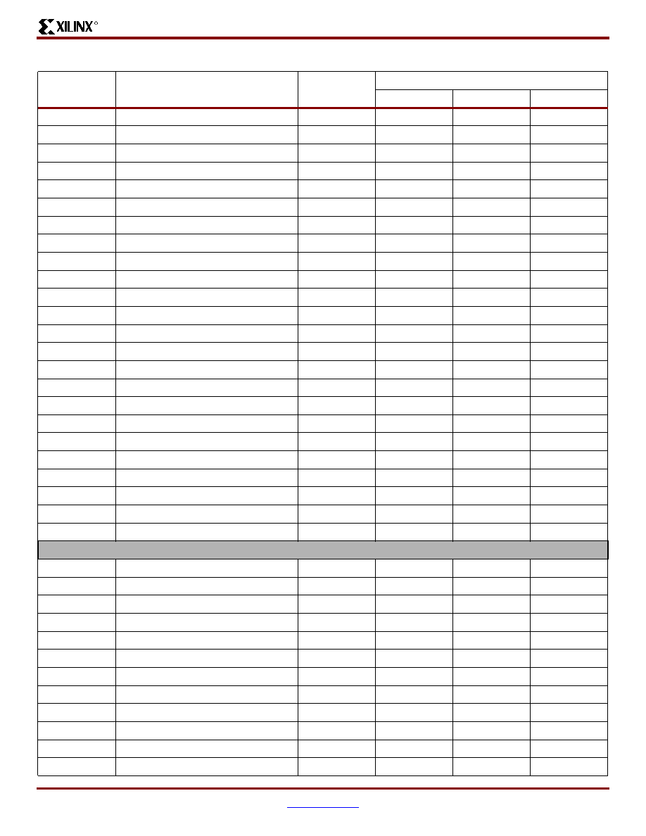
Virtex-II ProTM Platform FPGAs: Pinout Information
R
DS083-4 (v2.5.5) August 25, 2003
www.xilinx.com
239
Advance Product Specification
1-800-255-7778
N/A
RXPPAD21
BB31
N/A
GNDA21
AY31
N/A
TXPPAD21
BB32
N/A
TXNPAD21
BB33
N/A
VTTXPAD21
BA33
N/A
AVCCAUXTX21
BA32
N/A
AVCCAUXRX22
BA34
N/A
VTRXPAD22
BA35
N/A
RXNPAD22
BB34
N/A
RXPPAD22
BB35
N/A
GNDA22
AY35
N/A
TXPPAD22
BB36
N/A
TXNPAD22
BB37
N/A
VTTXPAD22
BA37
N/A
AVCCAUXTX22
BA36
N/A
AVCCAUXRX23
BA38
N/A
VTRXPAD23
BA39
N/A
RXNPAD23
BB38
N/A
RXPPAD23
BB39
N/A
GNDA23
AY39
N/A
TXPPAD23
BB40
N/A
TXNPAD23
BB41
N/A
VTTXPAD23
BA41
N/A
AVCCAUXTX23
BA40
N/A
VCCINT
AB27
N/A
VCCINT
AB16
N/A
VCCINT
AC27
N/A
VCCINT
AC16
N/A
VCCINT
AD27
N/A
VCCINT
AD16
N/A
VCCINT
AE27
N/A
VCCINT
AE16
N/A
VCCINT
AF27
N/A
VCCINT
AF26
N/A
VCCINT
AF17
N/A
VCCINT
AF16
Table 13: FF1704 -- XC2VP70, XC2VP100, and XC2VP125
Bank
Pin Description
Pin Number
No Connects
XC2VP70
XC2VP100
XC2VP125

FF1704 Flip-Chip Fine-Pitch BGA Package
R
240
www.xilinx.com
DS083-4 (v2.5.5) August 25, 2003
1-800-255-7778
Advance Product Specification
N/A
VCCINT
AG27
N/A
VCCINT
AG26
N/A
VCCINT
AG25
N/A
VCCINT
AG24
N/A
VCCINT
AG23
N/A
VCCINT
AG22
N/A
VCCINT
AG21
N/A
VCCINT
AG20
N/A
VCCINT
AG19
N/A
VCCINT
AG18
N/A
VCCINT
AG17
N/A
VCCINT
AG16
N/A
VCCINT
AH28
N/A
VCCINT
AH27
N/A
VCCINT
AH26
N/A
VCCINT
AH17
N/A
VCCINT
AH16
N/A
VCCINT
AH15
N/A
VCCINT
AJ29
N/A
VCCINT
AJ28
N/A
VCCINT
AJ27
N/A
VCCINT
AJ16
N/A
VCCINT
AJ15
N/A
VCCINT
AJ14
N/A
VCCINT
AK30
N/A
VCCINT
AK13
N/A
VCCINT
AA27
N/A
VCCINT
AA16
N/A
VCCINT
Y27
N/A
VCCINT
Y16
N/A
VCCINT
W27
N/A
VCCINT
W16
N/A
VCCINT
V27
N/A
VCCINT
V16
N/A
VCCINT
U27
N/A
VCCINT
U26
N/A
VCCINT
U17
Table 13: FF1704 -- XC2VP70, XC2VP100, and XC2VP125
Bank
Pin Description
Pin Number
No Connects
XC2VP70
XC2VP100
XC2VP125
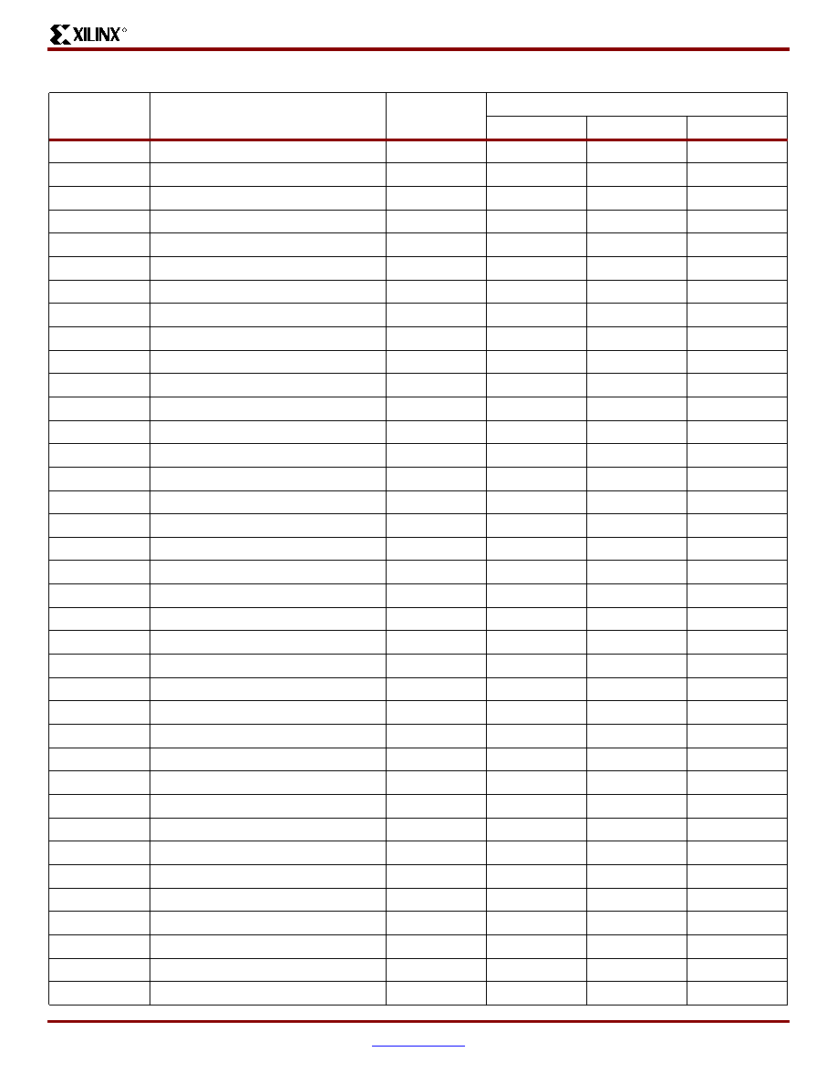
Virtex-II ProTM Platform FPGAs: Pinout Information
R
DS083-4 (v2.5.5) August 25, 2003
www.xilinx.com
241
Advance Product Specification
1-800-255-7778
N/A
VCCINT
U16
N/A
VCCINT
T27
N/A
VCCINT
T26
N/A
VCCINT
T25
N/A
VCCINT
T24
N/A
VCCINT
T23
N/A
VCCINT
T22
N/A
VCCINT
T21
N/A
VCCINT
T20
N/A
VCCINT
T19
N/A
VCCINT
T18
N/A
VCCINT
T17
N/A
VCCINT
T16
N/A
VCCINT
R28
N/A
VCCINT
R27
N/A
VCCINT
R26
N/A
VCCINT
R17
N/A
VCCINT
R16
N/A
VCCINT
R15
N/A
VCCINT
P29
N/A
VCCINT
P28
N/A
VCCINT
P27
N/A
VCCINT
P16
N/A
VCCINT
P15
N/A
VCCINT
P14
N/A
VCCINT
N30
N/A
VCCINT
N13
N/A
VCCAUX
AB42
N/A
VCCAUX
AB41
N/A
VCCAUX
AB2
N/A
VCCAUX
AB1
N/A
VCCAUX
AC42
N/A
VCCAUX
AC1
N/A
VCCAUX
AM32
N/A
VCCAUX
AM11
N/A
VCCAUX
AN33
N/A
VCCAUX
AN10
Table 13: FF1704 -- XC2VP70, XC2VP100, and XC2VP125
Bank
Pin Description
Pin Number
No Connects
XC2VP70
XC2VP100
XC2VP125

FF1704 Flip-Chip Fine-Pitch BGA Package
R
242
www.xilinx.com
DS083-4 (v2.5.5) August 25, 2003
1-800-255-7778
Advance Product Specification
N/A
VCCAUX
AV39
N/A
VCCAUX
AV4
N/A
VCCAUX
AW38
N/A
VCCAUX
AW22
N/A
VCCAUX
AW21
N/A
VCCAUX
AW5
N/A
VCCAUX
AA42
N/A
VCCAUX
AA41
N/A
VCCAUX
AA2
N/A
VCCAUX
AA1
N/A
VCCAUX
Y42
N/A
VCCAUX
Y1
N/A
VCCAUX
L32
N/A
VCCAUX
L11
N/A
VCCAUX
K33
N/A
VCCAUX
K10
N/A
VCCAUX
E39
N/A
VCCAUX
E4
N/A
VCCAUX
D38
N/A
VCCAUX
D22
N/A
VCCAUX
D21
N/A
VCCAUX
D5
N/A
GND
AB38
N/A
GND
AB35
N/A
GND
AB32
N/A
GND
AB26
N/A
GND
AB25
N/A
GND
AB24
N/A
GND
AB23
N/A
GND
AB22
N/A
GND
AB21
N/A
GND
AB20
N/A
GND
AB19
N/A
GND
AB18
N/A
GND
AB17
N/A
GND
AB11
N/A
GND
AB8
Table 13: FF1704 -- XC2VP70, XC2VP100, and XC2VP125
Bank
Pin Description
Pin Number
No Connects
XC2VP70
XC2VP100
XC2VP125

Virtex-II ProTM Platform FPGAs: Pinout Information
R
DS083-4 (v2.5.5) August 25, 2003
www.xilinx.com
243
Advance Product Specification
1-800-255-7778
N/A
GND
AB5
N/A
GND
AC41
N/A
GND
AC26
N/A
GND
AC25
N/A
GND
AC24
N/A
GND
AC23
N/A
GND
AC22
N/A
GND
AC21
N/A
GND
AC20
N/A
GND
AC19
N/A
GND
AC18
N/A
GND
AC17
N/A
GND
AC2
N/A
GND
AD26
N/A
GND
AD25
N/A
GND
AD24
N/A
GND
AD23
N/A
GND
AD22
N/A
GND
AD21
N/A
GND
AD20
N/A
GND
AD19
N/A
GND
AD18
N/A
GND
AD17
N/A
GND
AE37
N/A
GND
AE34
N/A
GND
AE26
N/A
GND
AE25
N/A
GND
AE24
N/A
GND
AE23
N/A
GND
AE22
N/A
GND
AE21
N/A
GND
AE20
N/A
GND
AE19
N/A
GND
AE18
N/A
GND
AE17
N/A
GND
AE9
N/A
GND
AE6
Table 13: FF1704 -- XC2VP70, XC2VP100, and XC2VP125
Bank
Pin Description
Pin Number
No Connects
XC2VP70
XC2VP100
XC2VP125

FF1704 Flip-Chip Fine-Pitch BGA Package
R
244
www.xilinx.com
DS083-4 (v2.5.5) August 25, 2003
1-800-255-7778
Advance Product Specification
N/A
GND
AF25
N/A
GND
AF24
N/A
GND
AF23
N/A
GND
AF22
N/A
GND
AF21
N/A
GND
AF20
N/A
GND
AF19
N/A
GND
AF18
N/A
GND
AG42
N/A
GND
AG1
N/A
GND
AH39
N/A
GND
AH36
N/A
GND
AH7
N/A
GND
AH4
N/A
GND
AL42
N/A
GND
AL1
N/A
GND
AM22
N/A
GND
AM21
N/A
GND
AN39
N/A
GND
AN4
N/A
GND
AP34
N/A
GND
AP9
N/A
GND
AR42
N/A
GND
AR35
N/A
GND
AR22
N/A
GND
AR21
N/A
GND
AR8
N/A
GND
AR1
N/A
GND
AT36
N/A
GND
AT7
N/A
GND
AU37
N/A
GND
AU25
N/A
GND
AU18
N/A
GND
AU6
N/A
GND
AV38
N/A
GND
AV22
N/A
GND
AV21
Table 13: FF1704 -- XC2VP70, XC2VP100, and XC2VP125
Bank
Pin Description
Pin Number
No Connects
XC2VP70
XC2VP100
XC2VP125

Virtex-II ProTM Platform FPGAs: Pinout Information
R
DS083-4 (v2.5.5) August 25, 2003
www.xilinx.com
245
Advance Product Specification
1-800-255-7778
N/A
GND
AV5
N/A
GND
AW39
N/A
GND
AW32
N/A
GND
AW28
N/A
GND
AW15
N/A
GND
AW11
N/A
GND
AW4
N/A
GND
AY42
N/A
GND
AY41
N/A
GND
AY40
N/A
GND
AY3
N/A
GND
AY2
N/A
GND
AY1
N/A
GND
BA42
N/A
GND
BA1
N/A
GND
AA38
N/A
GND
AA35
N/A
GND
AA32
N/A
GND
AA26
N/A
GND
AA25
N/A
GND
AA24
N/A
GND
AA23
N/A
GND
AA22
N/A
GND
AA21
N/A
GND
AA20
N/A
GND
AA19
N/A
GND
AA18
N/A
GND
AA17
N/A
GND
AA11
N/A
GND
AA8
N/A
GND
AA5
N/A
GND
Y41
N/A
GND
Y26
N/A
GND
Y25
N/A
GND
Y24
N/A
GND
Y23
N/A
GND
Y22
Table 13: FF1704 -- XC2VP70, XC2VP100, and XC2VP125
Bank
Pin Description
Pin Number
No Connects
XC2VP70
XC2VP100
XC2VP125

FF1704 Flip-Chip Fine-Pitch BGA Package
R
246
www.xilinx.com
DS083-4 (v2.5.5) August 25, 2003
1-800-255-7778
Advance Product Specification
N/A
GND
Y21
N/A
GND
Y20
N/A
GND
Y19
N/A
GND
Y18
N/A
GND
Y17
N/A
GND
Y2
N/A
GND
W26
N/A
GND
W25
N/A
GND
W24
N/A
GND
W23
N/A
GND
W22
N/A
GND
W21
N/A
GND
W20
N/A
GND
W19
N/A
GND
W18
N/A
GND
W17
N/A
GND
V37
N/A
GND
V34
N/A
GND
V26
N/A
GND
V25
N/A
GND
V24
N/A
GND
V23
N/A
GND
V22
N/A
GND
V21
N/A
GND
V20
N/A
GND
V19
N/A
GND
V18
N/A
GND
V17
N/A
GND
V9
N/A
GND
V6
N/A
GND
U25
N/A
GND
U24
N/A
GND
U23
N/A
GND
U22
N/A
GND
U21
N/A
GND
U20
N/A
GND
U19
Table 13: FF1704 -- XC2VP70, XC2VP100, and XC2VP125
Bank
Pin Description
Pin Number
No Connects
XC2VP70
XC2VP100
XC2VP125

Virtex-II ProTM Platform FPGAs: Pinout Information
R
DS083-4 (v2.5.5) August 25, 2003
www.xilinx.com
247
Advance Product Specification
1-800-255-7778
N/A
GND
U18
N/A
GND
T42
N/A
GND
T1
N/A
GND
R39
N/A
GND
R36
N/A
GND
R7
N/A
GND
R4
N/A
GND
M42
N/A
GND
M1
N/A
GND
L22
N/A
GND
L21
N/A
GND
K39
N/A
GND
K4
N/A
GND
J34
N/A
GND
J9
N/A
GND
H42
N/A
GND
H35
N/A
GND
H22
N/A
GND
H21
N/A
GND
H8
N/A
GND
H1
N/A
GND
G36
N/A
GND
G7
N/A
GND
F37
N/A
GND
F25
N/A
GND
F18
N/A
GND
F6
N/A
GND
E38
N/A
GND
E22
N/A
GND
E21
N/A
GND
E5
N/A
GND
D39
N/A
GND
D32
N/A
GND
D28
N/A
GND
D15
N/A
GND
D11
N/A
GND
D4
Table 13: FF1704 -- XC2VP70, XC2VP100, and XC2VP125
Bank
Pin Description
Pin Number
No Connects
XC2VP70
XC2VP100
XC2VP125
FF1704 Flip-Chip Fine-Pitch BGA Package
R
248
www.xilinx.com
DS083-4 (v2.5.5) August 25, 2003
1-800-255-7778
Advance Product Specification
N/A
GND
C42
N/A
GND
C41
N/A
GND
C40
N/A
GND
C3
N/A
GND
C2
N/A
GND
C1
N/A
GND
B42
N/A
GND
B1
N/A
GND
N14
N/A
GND
N29
N/A
GND
AK14
N/A
GND
AK29
N/A
GND
P13
N/A
GND
P30
N/A
GND
AJ13
N/A
GND
AJ30
Notes:
1.
See
Table 4
for an explanation of the signals available on this pin.
Table 13: FF1704 -- XC2VP70, XC2VP100, and XC2VP125
Bank
Pin Description
Pin Number
No Connects
XC2VP70
XC2VP100
XC2VP125
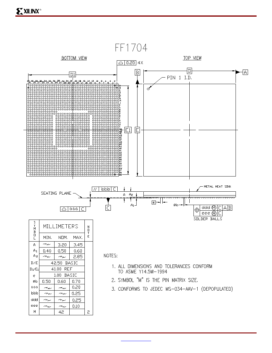
Virtex-II ProTM Platform FPGAs: Pinout Information
R
DS083-4 (v2.5.5) August 25, 2003
www.xilinx.com
249
Advance Product Specification
1-800-255-7778
FF1704 Flip-Chip Fine-Pitch BGA Package Specifications (1.00mm pitch)
Figure 9: FF1704 Flip-Chip Fine-Pitch BGA Package Specifications
FF1696 Flip-Chip Fine-Pitch BGA Package
R
250
www.xilinx.com
DS083-4 (v2.5.5) August 25, 2003
1-800-255-7778
Advance Product Specification
FF1696 Flip-Chip Fine-Pitch BGA Package
As shown in
Table 14
, XC2VP100 and XC2VP125 Virtex-II Pro devices are available in the FF1696 flip-chip fine-pitch BGA
package. Following this table are the
FF1696 Flip-Chip Fine-Pitch BGA Package Specifications (1.00mm pitch)
.
Table 14: FF1696 -- XC2VP100 and XC2VP125
Bank
Pin Description
Pin Number
No Connects
XC2VP100
XC2VP125
0
IO_L01N_0/VRP_0
E33
0
IO_L01P_0/VRN_0
F33
0
IO_L02N_0
K32
0
IO_L02P_0
L32
0
IO_L03N_0
C32
0
IO_L03P_0/VREF_0
C33
0
IO_L05_0/No_Pair
G33
0
IO_L06N_0
A33
0
IO_L06P_0
B33
0
IO_L07N_0
F32
0
IO_L07P_0
G32
0
IO_L08N_0
H32
0
IO_L08P_0
J32
0
IO_L09N_0
D32
0
IO_L09P_0/VREF_0
E32
0
IO_L19N_0
A32
0
IO_L19P_0
B32
0
IO_L20N_0
K31
0
IO_L20P_0
L31
0
IO_L21N_0
H30
0
IO_L21P_0
G31
0
IO_L25N_0
E31
0
IO_L25P_0
F31
0
IO_L26N_0
H31
0
IO_L26P_0
J31
0
IO_L27N_0
D30
0
IO_L27P_0/VREF_0
D31
0
IO_L28N_0
B31
0
IO_L28P_0
C31
0
IO_L29N_0
K30
0
IO_L29P_0
L30
0
IO_L30N_0
F30
0
IO_L30P_0
G30
0
IO_L34N_0
B30

Virtex-II ProTM Platform FPGAs: Pinout Information
R
DS083-4 (v2.5.5) August 25, 2003
www.xilinx.com
251
Advance Product Specification
1-800-255-7778
0
IO_L34P_0
C30
0
IO_L35N_0
L29
0
IO_L35P_0
M29
0
IO_L36N_0
H28
0
IO_L36P_0/VREF_0
G29
0
IO_L76N_0
E29
0
IO_L76P_0
F29
0
IO_L77N_0
J29
0
IO_L77P_0
K29
0
IO_L78N_0
D28
0
IO_L78P_0
C29
0
IO_L79N_0
A29
0
IO_L79P_0
B29
0
IO_L80_0/No_Pair
L28
0
IO_L83_0/No_Pair
M28
0
IO_L84N_0
G27
0
IO_L84P_0
G28
0
IO_L85N_0
E28
0
IO_L85P_0
F28
0
IO_L86N_0
J28
0
IO_L86P_0
K28
0
IO_L87N_0
C27
0
IO_L87P_0/VREF_0
C28
0
IO_L37N_0
A28
0
IO_L37P_0
B28
0
IO_L38N_0
L27
0
IO_L38P_0
M27
0
IO_L39N_0
H26
0
IO_L39P_0
H27
0
IO_L43N_0
E27
0
IO_L43P_0
F27
0
IO_L44N_0
J27
0
IO_L44P_0
K27
0
IO_L45N_0
D26
0
IO_L45P_0/VREF_0
D27
0
IO_L10N_0
A27
NC
0
IO_L10P_0
B27
NC
Table 14: FF1696 -- XC2VP100 and XC2VP125
Bank
Pin Description
Pin Number
No Connects
XC2VP100
XC2VP125

FF1696 Flip-Chip Fine-Pitch BGA Package
R
252
www.xilinx.com
DS083-4 (v2.5.5) August 25, 2003
1-800-255-7778
Advance Product Specification
0
IO_L11N_0
M25
NC
0
IO_L11P_0
M26
NC
0
IO_L12N_0
F26
NC
0
IO_L12P_0
G26
NC
0
IO_L18N_0
B26
NC
0
IO_L18P_0/VREF_0
C26
NC
0
IO_L46N_0
G24
0
IO_L46P_0
G25
0
IO_L47N_0
K26
0
IO_L47P_0
L26
0
IO_L48N_0
E25
0
IO_L48P_0
F25
0
IO_L49N_0
C24
0
IO_L49P_0
C25
0
IO_L50_0/No_Pair
L24
0
IO_L53_0/No_Pair
L25
0
IO_L54N_0
A25
0
IO_L54P_0
B25
0
IO_L55N_0
H23
0
IO_L55P_0
H24
0
IO_L56N_0
J25
0
IO_L56P_0
K25
0
IO_L57N_0
E24
0
IO_L57P_0/VREF_0
F24
0
IO_L58N_0
D23
0
IO_L58P_0
D24
0
IO_L59N_0
J24
0
IO_L59P_0
K24
0
IO_L60N_0
A24
0
IO_L60P_0
B24
0
IO_L64N_0
F23
0
IO_L64P_0
G23
0
IO_L65N_0
M22
0
IO_L65P_0
M23
0
IO_L66N_0
B23
0
IO_L66P_0/VREF_0
C23
0
IO_L67N_0
H22
Table 14: FF1696 -- XC2VP100 and XC2VP125
Bank
Pin Description
Pin Number
No Connects
XC2VP100
XC2VP125

Virtex-II ProTM Platform FPGAs: Pinout Information
R
DS083-4 (v2.5.5) August 25, 2003
www.xilinx.com
253
Advance Product Specification
1-800-255-7778
0
IO_L67P_0
J22
0
IO_L68N_0
K23
0
IO_L68P_0
L23
0
IO_L69N_0
F22
0
IO_L69P_0/VREF_0
G22
0
IO_L73N_0
D22
0
IO_L73P_0
E22
0
IO_L74N_0/GCLK7P
K22
0
IO_L74P_0/GCLK6S
L22
0
IO_L75N_0/GCLK5P
B22
0
IO_L75P_0/GCLK4S
C22
1
IO_L75N_1/GCLK3P
C21
1
IO_L75P_1/GCLK2S
B21
1
IO_L74N_1/GCLK1P
L21
1
IO_L74P_1/GCLK0S
K21
1
IO_L73N_1
E21
1
IO_L73P_1
D21
1
IO_L69N_1/VREF_1
G21
1
IO_L69P_1
F21
1
IO_L68N_1
L20
1
IO_L68P_1
K20
1
IO_L67N_1
J21
1
IO_L67P_1
H21
1
IO_L66N_1/VREF_1
C20
1
IO_L66P_1
B20
1
IO_L65N_1
M20
1
IO_L65P_1
M21
1
IO_L64N_1
G20
1
IO_L64P_1
F20
1
IO_L60N_1
B19
1
IO_L60P_1
A19
1
IO_L59N_1
K19
1
IO_L59P_1
J19
1
IO_L58N_1
D19
1
IO_L58P_1
D20
1
IO_L57N_1/VREF_1
F19
Table 14: FF1696 -- XC2VP100 and XC2VP125
Bank
Pin Description
Pin Number
No Connects
XC2VP100
XC2VP125

FF1696 Flip-Chip Fine-Pitch BGA Package
R
254
www.xilinx.com
DS083-4 (v2.5.5) August 25, 2003
1-800-255-7778
Advance Product Specification
1
IO_L57P_1
E19
1
IO_L56N_1
K18
1
IO_L56P_1
J18
1
IO_L55N_1
H19
1
IO_L55P_1
H20
1
IO_L54N_1
B18
1
IO_L54P_1
A18
1
IO_L53_1/No_Pair
L18
1
IO_L50_1/No_Pair
L19
1
IO_L49N_1
C18
1
IO_L49P_1
C19
1
IO_L48N_1
F18
1
IO_L48P_1
E18
1
IO_L47N_1
L17
1
IO_L47P_1
K17
1
IO_L46N_1
G18
1
IO_L46P_1
G19
1
IO_L18N_1/VREF_1
C17
NC
1
IO_L18P_1
B17
NC
1
IO_L12N_1
G17
NC
1
IO_L12P_1
F17
NC
1
IO_L11N_1
M17
NC
1
IO_L11P_1
M18
NC
1
IO_L10N_1
B16
NC
1
IO_L10P_1
A16
NC
1
IO_L45N_1/VREF_1
D16
1
IO_L45P_1
D17
1
IO_L44N_1
K16
1
IO_L44P_1
J16
1
IO_L43N_1
F16
1
IO_L43P_1
E16
1
IO_L39N_1
H16
1
IO_L39P_1
H17
1
IO_L38N_1
M16
1
IO_L38P_1
L16
1
IO_L37N_1
B15
1
IO_L37P_1
A15
Table 14: FF1696 -- XC2VP100 and XC2VP125
Bank
Pin Description
Pin Number
No Connects
XC2VP100
XC2VP125

Virtex-II ProTM Platform FPGAs: Pinout Information
R
DS083-4 (v2.5.5) August 25, 2003
www.xilinx.com
255
Advance Product Specification
1-800-255-7778
1
IO_L87N_1/VREF_1
C15
1
IO_L87P_1
C16
1
IO_L86N_1
K15
1
IO_L86P_1
J15
1
IO_L85N_1
F15
1
IO_L85P_1
E15
1
IO_L84N_1
G15
1
IO_L84P_1
G16
1
IO_L83_1/No_Pair
M15
1
IO_L80_1/No_Pair
L15
1
IO_L79N_1
B14
1
IO_L79P_1
A14
1
IO_L78N_1
C14
1
IO_L78P_1
D15
1
IO_L77N_1
K14
1
IO_L77P_1
J14
1
IO_L76N_1
F14
1
IO_L76P_1
E14
1
IO_L36N_1/VREF_1
G14
1
IO_L36P_1
H15
1
IO_L35N_1
M14
1
IO_L35P_1
L14
1
IO_L34N_1
C13
1
IO_L34P_1
B13
1
IO_L30N_1
G13
1
IO_L30P_1
F13
1
IO_L29N_1
L13
1
IO_L29P_1
K13
1
IO_L28N_1
C12
1
IO_L28P_1
B12
1
IO_L27N_1/VREF_1
D12
1
IO_L27P_1
D13
1
IO_L26N_1
J12
1
IO_L26P_1
H12
1
IO_L25N_1
F12
1
IO_L25P_1
E12
1
IO_L21N_1
G12
Table 14: FF1696 -- XC2VP100 and XC2VP125
Bank
Pin Description
Pin Number
No Connects
XC2VP100
XC2VP125
FF1696 Flip-Chip Fine-Pitch BGA Package
R
256
www.xilinx.com
DS083-4 (v2.5.5) August 25, 2003
1-800-255-7778
Advance Product Specification
1
IO_L21P_1
H13
1
IO_L20N_1
L12
1
IO_L20P_1
K12
1
IO_L19N_1
B11
1
IO_L19P_1
A11
1
IO_L09N_1/VREF_1
E11
1
IO_L09P_1
D11
1
IO_L08N_1
J11
1
IO_L08P_1
H11
1
IO_L07N_1
G11
1
IO_L07P_1
F11
1
IO_L06N_1
B10
1
IO_L06P_1
A10
1
IO_L05_1/No_Pair
G10
1
IO_L03N_1/VREF_1
C10
1
IO_L03P_1
C11
1
IO_L02N_1
L11
1
IO_L02P_1
K11
1
IO_L01N_1/VRP_1
F10
1
IO_L01P_1/VRN_1
E10
2
IO_L01N_2/VRP_2
B8
2
IO_L01P_2/VRN_2
A8
2
IO_L02N_2
C9
2
IO_L02P_2
B9
2
IO_L03N_2
B7
2
IO_L03P_2
A7
2
IO_L04N_2/VREF_2
B6
2
IO_L04P_2
A6
2
IO_L05N_2
D8
2
IO_L05P_2
D9
2
IO_L06N_2
B4
2
IO_L06P_2
A4
2
IO_L73N_2
C7
2
IO_L73P_2
C8
2
IO_L74N_2
G9
2
IO_L74P_2
F9
Table 14: FF1696 -- XC2VP100 and XC2VP125
Bank
Pin Description
Pin Number
No Connects
XC2VP100
XC2VP125
Virtex-II ProTM Platform FPGAs: Pinout Information
R
DS083-4 (v2.5.5) August 25, 2003
www.xilinx.com
257
Advance Product Specification
1-800-255-7778
2
IO_L75N_2
C5
2
IO_L75P_2
B5
2
IO_L76N_2/VREF_2
D7
2
IO_L76P_2
C6
2
IO_L77N_2
H8
2
IO_L77P_2
H9
2
IO_L78N_2
C3
2
IO_L78P_2
C4
2
IO_L79N_2
D1
2
IO_L79P_2
D2
2
IO_L80N_2
J8
2
IO_L80P_2
K9
2
IO_L81N_2
E6
2
IO_L81P_2
D5
2
IO_L82N_2/VREF_2
E4
2
IO_L82P_2
D4
2
IO_L83N_2
L8
2
IO_L83P_2
L9
2
IO_L84N_2
E3
2
IO_L84P_2
D3
2
IO_L61N_2
F8
2
IO_L61P_2
E8
2
IO_L62N_2
M8
2
IO_L62P_2
M9
2
IO_L63N_2
F7
2
IO_L63P_2
E7
2
IO_L64N_2/VREF_2
F3
2
IO_L64P_2
E2
2
IO_L65N_2
N12
2
IO_L65P_2
P12
2
IO_L66N_2
F1
2
IO_L66P_2
F2
2
IO_L67N_2
G7
2
IO_L67P_2
G8
2
IO_L68N_2
N10
2
IO_L68P_2
N11
2
IO_L69N_2
G6
Table 14: FF1696 -- XC2VP100 and XC2VP125
Bank
Pin Description
Pin Number
No Connects
XC2VP100
XC2VP125

FF1696 Flip-Chip Fine-Pitch BGA Package
R
258
www.xilinx.com
DS083-4 (v2.5.5) August 25, 2003
1-800-255-7778
Advance Product Specification
2
IO_L69P_2
F6
2
IO_L70N_2/VREF_2
G5
2
IO_L70P_2
F5
2
IO_L71N_2
P10
2
IO_L71P_2
P11
2
IO_L72N_2
G3
2
IO_L72P_2
G4
2
IO_L07N_2
G1
2
IO_L07P_2
G2
2
IO_L08N_2
N8
2
IO_L08P_2
P9
2
IO_L09N_2
H6
2
IO_L09P_2
H7
2
IO_L10N_2/VREF_2
H4
2
IO_L10P_2
H5
2
IO_L11N_2
R12
2
IO_L11P_2
T12
2
IO_L12N_2
H2
2
IO_L12P_2
H3
2
IO_L13N_2
J6
2
IO_L13P_2
J7
2
IO_L14N_2
R10
2
IO_L14P_2
R11
2
IO_L15N_2
J3
2
IO_L15P_2
J4
2
IO_L16N_2/VREF_2
J2
2
IO_L16P_2
H1
2
IO_L17N_2
R8
2
IO_L17P_2
R9
2
IO_L18N_2
K5
2
IO_L18P_2
K6
2
IO_L19N_2
K1
2
IO_L19P_2
K2
2
IO_L20N_2
T10
2
IO_L20P_2
T11
2
IO_L21N_2
L7
2
IO_L21P_2
K7
Table 14: FF1696 -- XC2VP100 and XC2VP125
Bank
Pin Description
Pin Number
No Connects
XC2VP100
XC2VP125

Virtex-II ProTM Platform FPGAs: Pinout Information
R
DS083-4 (v2.5.5) August 25, 2003
www.xilinx.com
259
Advance Product Specification
1-800-255-7778
2
IO_L22N_2/VREF_2
L4
2
IO_L22P_2
L5
2
IO_L23N_2
T8
2
IO_L23P_2
T9
2
IO_L24N_2
L3
2
IO_L24P_2
K3
2
IO_L25N_2
L1
2
IO_L25P_2
L2
2
IO_L26N_2
U12
2
IO_L26P_2
V12
2
IO_L27N_2
M7
2
IO_L27P_2
L6
2
IO_L28N_2/VREF_2
M5
2
IO_L28P_2
M6
2
IO_L29N_2
U10
2
IO_L29P_2
U11
2
IO_L30N_2
M3
2
IO_L30P_2
M4
2
IO_L31N_2
N6
2
IO_L31P_2
N7
2
IO_L32N_2
U7
2
IO_L32P_2
U8
2
IO_L33N_2
N3
2
IO_L33P_2
N4
2
IO_L34N_2/VREF_2
N2
2
IO_L34P_2
M2
2
IO_L35N_2
V10
2
IO_L35P_2
V11
2
IO_L36N_2
P6
2
IO_L36P_2
P7
2
IO_L37N_2
P1
2
IO_L37P_2
P2
2
IO_L38N_2
V8
2
IO_L38P_2
V9
2
IO_L39N_2
R6
2
IO_L39P_2
P5
2
IO_L40N_2/VREF_2
R4
Table 14: FF1696 -- XC2VP100 and XC2VP125
Bank
Pin Description
Pin Number
No Connects
XC2VP100
XC2VP125

FF1696 Flip-Chip Fine-Pitch BGA Package
R
260
www.xilinx.com
DS083-4 (v2.5.5) August 25, 2003
1-800-255-7778
Advance Product Specification
2
IO_L40P_2
R5
2
IO_L41N_2
V6
2
IO_L41P_2
V7
2
IO_L42N_2
R3
2
IO_L42P_2
P3
2
IO_L43N_2
R1
2
IO_L43P_2
R2
2
IO_L44N_2
W10
2
IO_L44P_2
W11
2
IO_L45N_2
T7
2
IO_L45P_2
R7
2
IO_L46N_2/VREF_2
T4
2
IO_L46P_2
T5
2
IO_L47N_2
W9
2
IO_L47P_2
Y10
2
IO_L48N_2
T1
2
IO_L48P_2
T2
2
IO_L49N_2
U6
2
IO_L49P_2
T6
2
IO_L50N_2
W7
2
IO_L50P_2
Y8
2
IO_L51N_2
U4
2
IO_L51P_2
T3
2
IO_L52N_2/VREF_2
U2
2
IO_L52P_2
U3
2
IO_L53N_2
Y11
2
IO_L53P_2
Y12
2
IO_L54N_2
V4
2
IO_L54P_2
V5
2
IO_L55N_2
V1
2
IO_L55P_2
V2
2
IO_L56N_2
Y6
2
IO_L56P_2
Y7
2
IO_L57N_2
W5
2
IO_L57P_2
W6
2
IO_L58N_2/VREF_2
W3
2
IO_L58P_2
V3
Table 14: FF1696 -- XC2VP100 and XC2VP125
Bank
Pin Description
Pin Number
No Connects
XC2VP100
XC2VP125
Virtex-II ProTM Platform FPGAs: Pinout Information
R
DS083-4 (v2.5.5) August 25, 2003
www.xilinx.com
261
Advance Product Specification
1-800-255-7778
2
IO_L59N_2
AA11
2
IO_L59P_2
AA12
2
IO_L60N_2
W1
2
IO_L60P_2
W2
2
IO_L85N_2
Y2
2
IO_L85P_2
Y3
2
IO_L86N_2
AA9
2
IO_L86P_2
AA10
2
IO_L87N_2
AA5
2
IO_L87P_2
AA6
2
IO_L88N_2/VREF_2
AA4
2
IO_L88P_2
Y4
2
IO_L89N_2
AA7
2
IO_L89P_2
AA8
2
IO_L90N_2
AA2
2
IO_L90P_2
AA3
3
IO_L90N_3
AB5
3
IO_L90P_3
AB6
3
IO_L89N_3
AB11
3
IO_L89P_3
AB12
3
IO_L88N_3
AB2
3
IO_L88P_3
AB3
3
IO_L87N_3/VREF_3
AB4
3
IO_L87P_3
AC4
3
IO_L86N_3
AB9
3
IO_L86P_3
AB10
3
IO_L85N_3
AC2
3
IO_L85P_3
AC3
3
IO_L60N_3
AD5
3
IO_L60P_3
AD6
3
IO_L59N_3
AB7
3
IO_L59P_3
AB8
3
IO_L58N_3
AD1
3
IO_L58P_3
AD2
3
IO_L57N_3/VREF_3
AE4
3
IO_L57P_3
AE5
Table 14: FF1696 -- XC2VP100 and XC2VP125
Bank
Pin Description
Pin Number
No Connects
XC2VP100
XC2VP125

FF1696 Flip-Chip Fine-Pitch BGA Package
R
262
www.xilinx.com
DS083-4 (v2.5.5) August 25, 2003
1-800-255-7778
Advance Product Specification
3
IO_L56N_3
AC11
3
IO_L56P_3
AC12
3
IO_L55N_3
AD3
3
IO_L55P_3
AE3
3
IO_L54N_3
AE1
3
IO_L54P_3
AE2
3
IO_L53N_3
AC6
3
IO_L53P_3
AC7
3
IO_L52N_3
AF2
3
IO_L52P_3
AF3
3
IO_L51N_3/VREF_3
AF6
3
IO_L51P_3
AG6
3
IO_L50N_3
AD10
3
IO_L50P_3
AD11
3
IO_L49N_3
AG4
3
IO_L49P_3
AG5
3
IO_L48N_3
AF4
3
IO_L48P_3
AG3
3
IO_L47N_3
AC10
3
IO_L47P_3
AD9
3
IO_L46N_3
AG1
3
IO_L46P_3
AG2
3
IO_L45N_3/VREF_3
AG7
3
IO_L45P_3
AH7
3
IO_L44N_3
AC8
3
IO_L44P_3
AD7
3
IO_L43N_3
AH4
3
IO_L43P_3
AH5
3
IO_L42N_3
AH1
3
IO_L42P_3
AH2
3
IO_L41N_3
AE10
3
IO_L41P_3
AE11
3
IO_L40N_3
AJ6
3
IO_L40P_3
AJ7
3
IO_L39N_3/VREF_3
AH6
3
IO_L39P_3
AJ5
3
IO_L38N_3
AE8
Table 14: FF1696 -- XC2VP100 and XC2VP125
Bank
Pin Description
Pin Number
No Connects
XC2VP100
XC2VP125

Virtex-II ProTM Platform FPGAs: Pinout Information
R
DS083-4 (v2.5.5) August 25, 2003
www.xilinx.com
263
Advance Product Specification
1-800-255-7778
3
IO_L38P_3
AE9
3
IO_L37N_3
AH3
3
IO_L37P_3
AJ3
3
IO_L36N_3
AJ1
3
IO_L36P_3
AJ2
3
IO_L35N_3
AE6
3
IO_L35P_3
AE7
3
IO_L34N_3
AK6
3
IO_L34P_3
AK7
3
IO_L33N_3/VREF_3
AK3
3
IO_L33P_3
AK4
3
IO_L32N_3
AE12
3
IO_L32P_3
AF12
3
IO_L31N_3
AL5
3
IO_L31P_3
AL6
3
IO_L30N_3
AL3
3
IO_L30P_3
AL4
3
IO_L29N_3
AF10
3
IO_L29P_3
AF11
3
IO_L28N_3
AK2
3
IO_L28P_3
AL2
3
IO_L27N_3/VREF_3
AL7
3
IO_L27P_3
AM6
3
IO_L26N_3
AF7
3
IO_L26P_3
AF8
3
IO_L25N_3
AM4
3
IO_L25P_3
AM5
3
IO_L24N_3
AM1
3
IO_L24P_3
AM2
3
IO_L23N_3
AG10
3
IO_L23P_3
AG11
3
IO_L22N_3
AM7
3
IO_L22P_3
AN7
3
IO_L21N_3/VREF_3
AN5
3
IO_L21P_3
AN6
3
IO_L20N_3
AG8
3
IO_L20P_3
AG9
Table 14: FF1696 -- XC2VP100 and XC2VP125
Bank
Pin Description
Pin Number
No Connects
XC2VP100
XC2VP125

FF1696 Flip-Chip Fine-Pitch BGA Package
R
264
www.xilinx.com
DS083-4 (v2.5.5) August 25, 2003
1-800-255-7778
Advance Product Specification
3
IO_L19N_3
AM3
3
IO_L19P_3
AN3
3
IO_L18N_3
AN1
3
IO_L18P_3
AN2
3
IO_L17N_3
AG12
3
IO_L17P_3
AH12
3
IO_L16N_3
AP6
3
IO_L16P_3
AP7
3
IO_L15N_3/VREF_3
AP3
3
IO_L15P_3
AP4
3
IO_L14N_3
AH10
3
IO_L14P_3
AH11
3
IO_L13N_3
AR6
3
IO_L13P_3
AR7
3
IO_L12N_3
AR4
3
IO_L12P_3
AR5
3
IO_L11N_3
AH8
3
IO_L11P_3
AH9
3
IO_L10N_3
AR2
3
IO_L10P_3
AR3
3
IO_L09N_3/VREF_3
AP2
3
IO_L09P_3
AR1
3
IO_L08N_3
AJ10
3
IO_L08P_3
AJ11
3
IO_L07N_3
AT7
3
IO_L07P_3
AT8
3
IO_L72N_3
AT3
3
IO_L72P_3
AT4
3
IO_L71N_3
AJ12
3
IO_L71P_3
AK12
3
IO_L70N_3
AT1
3
IO_L70P_3
AT2
3
IO_L69N_3/VREF_3
AT6
3
IO_L69P_3
AU6
3
IO_L68N_3
AK10
3
IO_L68P_3
AK11
3
IO_L67N_3
AT5
Table 14: FF1696 -- XC2VP100 and XC2VP125
Bank
Pin Description
Pin Number
No Connects
XC2VP100
XC2VP125

Virtex-II ProTM Platform FPGAs: Pinout Information
R
DS083-4 (v2.5.5) August 25, 2003
www.xilinx.com
265
Advance Product Specification
1-800-255-7778
3
IO_L67P_3
AU5
3
IO_L66N_3
AU1
3
IO_L66P_3
AU2
3
IO_L65N_3
AJ9
3
IO_L65P_3
AK8
3
IO_L64N_3
AU8
3
IO_L64P_3
AV8
3
IO_L63N_3/VREF_3
AU7
3
IO_L63P_3
AV7
3
IO_L62N_3
AL8
3
IO_L62P_3
AL9
3
IO_L61N_3
AU3
3
IO_L61P_3
AV2
3
IO_L84N_3
AV6
3
IO_L84P_3
AW5
3
IO_L83N_3
AM8
3
IO_L83P_3
AM9
3
IO_L82N_3
AV4
3
IO_L82P_3
AW4
3
IO_L81N_3/VREF_3
AV3
3
IO_L81P_3
AW3
3
IO_L80N_3
AN9
3
IO_L80P_3
AP8
3
IO_L79N_3
AW1
3
IO_L79P_3
AW2
3
IO_L78N_3
AY7
3
IO_L78P_3
AY8
3
IO_L77N_3
AR8
3
IO_L77P_3
AR9
3
IO_L76N_3
AW7
3
IO_L76P_3
AY6
3
IO_L75N_3/VREF_3
AY3
3
IO_L75P_3
AY4
3
IO_L74N_3
AT9
3
IO_L74P_3
AU9
3
IO_L73N_3
AY5
3
IO_L73P_3
BA5
Table 14: FF1696 -- XC2VP100 and XC2VP125
Bank
Pin Description
Pin Number
No Connects
XC2VP100
XC2VP125
FF1696 Flip-Chip Fine-Pitch BGA Package
R
266
www.xilinx.com
DS083-4 (v2.5.5) August 25, 2003
1-800-255-7778
Advance Product Specification
3
IO_L06N_3
BA8
3
IO_L06P_3
BB8
3
IO_L05N_3
AW8
3
IO_L05P_3
AW9
3
IO_L04N_3
BA7
3
IO_L04P_3
BB7
3
IO_L03N_3/VREF_3
BA6
3
IO_L03P_3
BB6
3
IO_L02N_3
AY9
3
IO_L02P_3
BA9
3
IO_L01N_3/VRP_3
BA4
3
IO_L01P_3/VRN_3
BB4
4
IO_L01N_4/BUSY/DOUT
(1)
AL11
4
IO_L01P_4/INIT_B
AL12
4
IO_L02N_4/D0/DIN
(1)
AV10
4
IO_L02P_4/D1
AU10
4
IO_L03N_4/D2
AN11
4
IO_L03P_4/D3
AM11
4
IO_L05_4/No_Pair
AT10
4
IO_L06N_4/VRP_4
AY11
4
IO_L06P_4/VRN_4
AY10
4
IO_L07N_4
BB10
4
IO_L07P_4/VREF_4
BA10
4
IO_L08N_4
AU11
4
IO_L08P_4
AT11
4
IO_L09N_4
AR11
4
IO_L09P_4/VREF_4
AP11
4
IO_L19N_4
AW11
4
IO_L19P_4
AV11
4
IO_L20N_4
BB11
4
IO_L20P_4
BA11
4
IO_L21N_4
AN12
4
IO_L21P_4
AM12
4
IO_L25N_4
AR13
4
IO_L25P_4
AT12
4
IO_L26N_4
AV12
Table 14: FF1696 -- XC2VP100 and XC2VP125
Bank
Pin Description
Pin Number
No Connects
XC2VP100
XC2VP125

Virtex-II ProTM Platform FPGAs: Pinout Information
R
DS083-4 (v2.5.5) August 25, 2003
www.xilinx.com
267
Advance Product Specification
1-800-255-7778
4
IO_L26P_4
AU12
4
IO_L27N_4
AR12
4
IO_L27P_4/VREF_4
AP12
4
IO_L28N_4
AW13
4
IO_L28P_4
AW12
4
IO_L29N_4
BA12
4
IO_L29P_4
AY12
4
IO_L30N_4
AN13
4
IO_L30P_4
AM13
4
IO_L34N_4
AU13
4
IO_L34P_4
AT13
4
IO_L35N_4
BA13
4
IO_L35P_4
AY13
4
IO_L36N_4
AM14
4
IO_L36P_4/VREF_4
AL14
4
IO_L76N_4
AR15
4
IO_L76P_4
AT14
4
IO_L77N_4
AV14
4
IO_L77P_4
AU14
4
IO_L78N_4
AP14
4
IO_L78P_4
AN14
4
IO_L79N_4
AW15
4
IO_L79P_4
AY14
4
IO_L80_4/No_Pair
BB14
4
IO_L83_4/No_Pair
BA14
4
IO_L84N_4
AM15
4
IO_L84P_4
AL15
4
IO_L85N_4
AT16
4
IO_L85P_4
AT15
4
IO_L86N_4
AV15
4
IO_L86P_4
AU15
4
IO_L87N_4
AP15
4
IO_L87P_4/VREF_4
AN15
4
IO_L37N_4
AY16
4
IO_L37P_4
AY15
4
IO_L38N_4
BB15
4
IO_L38P_4
BA15
Table 14: FF1696 -- XC2VP100 and XC2VP125
Bank
Pin Description
Pin Number
No Connects
XC2VP100
XC2VP125

FF1696 Flip-Chip Fine-Pitch BGA Package
R
268
www.xilinx.com
DS083-4 (v2.5.5) August 25, 2003
1-800-255-7778
Advance Product Specification
4
IO_L39N_4
AM16
4
IO_L39P_4
AL16
4
IO_L43N_4
AR17
4
IO_L43P_4
AR16
4
IO_L44N_4
AV16
4
IO_L44P_4
AU16
4
IO_L45N_4
AP16
4
IO_L45P_4/VREF_4
AN16
4
IO_L10N_4
AW17
NC
4
IO_L10P_4
AW16
NC
4
IO_L11N_4
BB16
NC
4
IO_L11P_4
BA16
NC
4
IO_L12N_4
AL18
NC
4
IO_L12P_4
AL17
NC
4
IO_L16N_4
AU17
NC
4
IO_L16P_4
AT17
NC
4
IO_L18N_4
BA17
NC
4
IO_L18P_4/VREF_4
AY17
NC
4
IO_L46N_4
AT19
4
IO_L46P_4
AT18
4
IO_L47N_4
AN17
4
IO_L47P_4
AM17
4
IO_L48N_4
AV18
4
IO_L48P_4
AU18
4
IO_L49N_4
AY19
4
IO_L49P_4
AY18
4
IO_L50_4/No_Pair
AM19
4
IO_L53_4/No_Pair
AM18
4
IO_L54N_4
BB18
4
IO_L54P_4
BA18
4
IO_L55N_4
AR20
4
IO_L55P_4
AR19
4
IO_L56N_4
AP18
4
IO_L56P_4
AN18
4
IO_L57N_4
AV19
4
IO_L57P_4/VREF_4
AU19
4
IO_L58N_4
AW20
Table 14: FF1696 -- XC2VP100 and XC2VP125
Bank
Pin Description
Pin Number
No Connects
XC2VP100
XC2VP125
Virtex-II ProTM Platform FPGAs: Pinout Information
R
DS083-4 (v2.5.5) August 25, 2003
www.xilinx.com
269
Advance Product Specification
1-800-255-7778
4
IO_L58P_4
AW19
4
IO_L59N_4
AP19
4
IO_L59P_4
AN19
4
IO_L60N_4
BB19
4
IO_L60P_4
BA19
4
IO_L64N_4
AU20
4
IO_L64P_4
AT20
4
IO_L65N_4
AL21
4
IO_L65P_4
AL20
4
IO_L66N_4
BA20
4
IO_L66P_4/VREF_4
AY20
4
IO_L67N_4
AR21
4
IO_L67P_4
AP21
4
IO_L68N_4
AN20
4
IO_L68P_4
AM20
4
IO_L69N_4
AU21
4
IO_L69P_4/VREF_4
AT21
4
IO_L73N_4
AW21
4
IO_L73P_4
AV21
4
IO_L74N_4/GCLK3S
AN21
4
IO_L74P_4/GCLK2P
AM21
4
IO_L75N_4/GCLK1S
BA21
4
IO_L75P_4/GCLK0P
AY21
5
IO_L75N_5/GCLK7S
AY22
5
IO_L75P_5/GCLK6P
BA22
5
IO_L74N_5/GCLK5S
AM22
5
IO_L74P_5/GCLK4P
AN22
5
IO_L73N_5
AV22
5
IO_L73P_5
AW22
5
IO_L69N_5/VREF_5
AT22
5
IO_L69P_5
AU22
5
IO_L68N_5
AM23
5
IO_L68P_5
AN23
5
IO_L67N_5
AP22
5
IO_L67P_5
AR22
5
IO_L66N_5/VREF_5
AY23
Table 14: FF1696 -- XC2VP100 and XC2VP125
Bank
Pin Description
Pin Number
No Connects
XC2VP100
XC2VP125

FF1696 Flip-Chip Fine-Pitch BGA Package
R
270
www.xilinx.com
DS083-4 (v2.5.5) August 25, 2003
1-800-255-7778
Advance Product Specification
5
IO_L66P_5
BA23
5
IO_L65N_5
AL23
5
IO_L65P_5
AL22
5
IO_L64N_5
AT23
5
IO_L64P_5
AU23
5
IO_L60N_5
BA24
5
IO_L60P_5
BB24
5
IO_L59N_5
AN24
5
IO_L59P_5
AP24
5
IO_L58N_5
AW24
5
IO_L58P_5
AW23
5
IO_L57N_5/VREF_5
AU24
5
IO_L57P_5
AV24
5
IO_L56N_5
AN25
5
IO_L56P_5
AP25
5
IO_L55N_5
AR24
5
IO_L55P_5
AR23
5
IO_L54N_5
BA25
5
IO_L54P_5
BB25
5
IO_L53_5/No_Pair
AM25
5
IO_L50_5/No_Pair
AM24
5
IO_L49N_5
AY25
5
IO_L49P_5
AY24
5
IO_L48N_5
AU25
5
IO_L48P_5
AV25
5
IO_L47N_5
AM26
5
IO_L47P_5
AN26
5
IO_L46N_5
AT25
5
IO_L46P_5
AT24
5
IO_L18N_5/VREF_5
AY26
NC
5
IO_L18P_5
BA26
NC
5
IO_L16N_5
AT26
NC
5
IO_L16P_5
AU26
NC
5
IO_L12N_5
AL26
NC
5
IO_L12P_5
AL25
NC
5
IO_L11N_5
BA27
NC
5
IO_L11P_5
BB27
NC
Table 14: FF1696 -- XC2VP100 and XC2VP125
Bank
Pin Description
Pin Number
No Connects
XC2VP100
XC2VP125

Virtex-II ProTM Platform FPGAs: Pinout Information
R
DS083-4 (v2.5.5) August 25, 2003
www.xilinx.com
271
Advance Product Specification
1-800-255-7778
5
IO_L10N_5
AW27
NC
5
IO_L10P_5
AW26
NC
5
IO_L45N_5/VREF_5
AN27
5
IO_L45P_5
AP27
5
IO_L44N_5
AU27
5
IO_L44P_5
AV27
5
IO_L43N_5
AR27
5
IO_L43P_5
AR26
5
IO_L39N_5
AL27
5
IO_L39P_5
AM27
5
IO_L38N_5
BA28
5
IO_L38P_5
BB28
5
IO_L37N_5
AY28
5
IO_L37P_5
AY27
5
IO_L87N_5/VREF_5
AN28
5
IO_L87P_5
AP28
5
IO_L86N_5
AU28
5
IO_L86P_5
AV28
5
IO_L85N_5
AT28
5
IO_L85P_5
AT27
5
IO_L84N_5
AL28
5
IO_L84P_5
AM28
5
IO_L83_5/No_Pair
BA29
5
IO_L80_5/No_Pair
BB29
5
IO_L79N_5
AY29
5
IO_L79P_5
AW28
5
IO_L78N_5
AN29
5
IO_L78P_5
AP29
5
IO_L77N_5
AU29
5
IO_L77P_5
AV29
5
IO_L76N_5
AT29
5
IO_L76P_5
AR28
5
IO_L36N_5/VREF_5
AL29
5
IO_L36P_5
AM29
5
IO_L35N_5
AY30
5
IO_L35P_5
BA30
5
IO_L34N_5
AT30
Table 14: FF1696 -- XC2VP100 and XC2VP125
Bank
Pin Description
Pin Number
No Connects
XC2VP100
XC2VP125
FF1696 Flip-Chip Fine-Pitch BGA Package
R
272
www.xilinx.com
DS083-4 (v2.5.5) August 25, 2003
1-800-255-7778
Advance Product Specification
5
IO_L34P_5
AU30
5
IO_L30N_5
AM30
5
IO_L30P_5
AN30
5
IO_L29N_5
AY31
5
IO_L29P_5
BA31
5
IO_L28N_5
AW31
5
IO_L28P_5
AW30
5
IO_L27N_5/VREF_5
AP31
5
IO_L27P_5
AR31
5
IO_L26N_5
AU31
5
IO_L26P_5
AV31
5
IO_L25N_5
AT31
5
IO_L25P_5
AR30
5
IO_L21N_5
AM31
5
IO_L21P_5
AN31
5
IO_L20N_5
BA32
5
IO_L20P_5
BB32
5
IO_L19N_5
AV32
5
IO_L19P_5
AW32
5
IO_L09N_5/VREF_5
AP32
5
IO_L09P_5
AR32
5
IO_L08N_5
AT32
5
IO_L08P_5
AU32
5
IO_L07N_5/VREF_5
BA33
5
IO_L07P_5
BB33
5
IO_L06N_5/VRP_5
AY33
5
IO_L06P_5/VRN_5
AY32
5
IO_L05_5/No_Pair
AT33
5
IO_L03N_5/D4
AM32
5
IO_L03P_5/D5
AN32
5
IO_L02N_5/D6
AU33
5
IO_L02P_5/D7
AV33
5
IO_L01N_5/RDWR_B
AL31
5
IO_L01P_5/CS_B
AL32
6
IO_L01P_6/VRN_6
BB39
6
IO_L01N_6/VRP_6
BA39
Table 14: FF1696 -- XC2VP100 and XC2VP125
Bank
Pin Description
Pin Number
No Connects
XC2VP100
XC2VP125

Virtex-II ProTM Platform FPGAs: Pinout Information
R
DS083-4 (v2.5.5) August 25, 2003
www.xilinx.com
273
Advance Product Specification
1-800-255-7778
6
IO_L02P_6
BA34
6
IO_L02N_6
AY34
6
IO_L03P_6
BB37
6
IO_L03N_6/VREF_6
BA37
6
IO_L04P_6
BB36
6
IO_L04N_6
BA36
6
IO_L05P_6
AW34
6
IO_L05N_6
AW35
6
IO_L06P_6
BB35
6
IO_L06N_6
BA35
6
IO_L73P_6
BA38
6
IO_L73N_6
AY38
6
IO_L74P_6
AU34
6
IO_L74N_6
AT34
6
IO_L75P_6
AY39
6
IO_L75N_6/VREF_6
AY40
6
IO_L76P_6
AY37
6
IO_L76N_6
AW36
6
IO_L77P_6
AR34
6
IO_L77N_6
AR35
6
IO_L78P_6
AY35
6
IO_L78N_6
AY36
6
IO_L79P_6
AW41
6
IO_L79N_6
AW42
6
IO_L80P_6
AP35
6
IO_L80N_6
AN34
6
IO_L81P_6
AW40
6
IO_L81N_6/VREF_6
AV40
6
IO_L82P_6
AW39
6
IO_L82N_6
AV39
6
IO_L83P_6
AM34
6
IO_L83N_6
AM35
6
IO_L84P_6
AW38
6
IO_L84N_6
AV37
6
IO_L61P_6
AV41
6
IO_L61N_6
AU40
6
IO_L62P_6
AL34
Table 14: FF1696 -- XC2VP100 and XC2VP125
Bank
Pin Description
Pin Number
No Connects
XC2VP100
XC2VP125
FF1696 Flip-Chip Fine-Pitch BGA Package
R
274
www.xilinx.com
DS083-4 (v2.5.5) August 25, 2003
1-800-255-7778
Advance Product Specification
6
IO_L62N_6
AL35
6
IO_L63P_6
AV36
6
IO_L63N_6/VREF_6
AU36
6
IO_L64P_6
AV35
6
IO_L64N_6
AU35
6
IO_L65P_6
AK35
6
IO_L65N_6
AJ34
6
IO_L66P_6
AU41
6
IO_L66N_6
AU42
6
IO_L67P_6
AU38
6
IO_L67N_6
AT38
6
IO_L68P_6
AK32
6
IO_L68N_6
AK33
6
IO_L69P_6
AU37
6
IO_L69N_6/VREF_6
AT37
6
IO_L70P_6
AT41
6
IO_L70N_6
AT42
6
IO_L71P_6
AK31
6
IO_L71N_6
AJ31
6
IO_L72P_6
AT39
6
IO_L72N_6
AT40
6
IO_L07P_6
AT35
6
IO_L07N_6
AT36
6
IO_L08P_6
AJ32
6
IO_L08N_6
AJ33
6
IO_L09P_6
AR42
6
IO_L09N_6/VREF_6
AP41
6
IO_L10P_6
AR40
6
IO_L10N_6
AR41
6
IO_L11P_6
AH34
6
IO_L11N_6
AH35
6
IO_L12P_6
AR38
6
IO_L12N_6
AR39
6
IO_L13P_6
AR36
6
IO_L13N_6
AR37
6
IO_L14P_6
AH32
6
IO_L14N_6
AH33
Table 14: FF1696 -- XC2VP100 and XC2VP125
Bank
Pin Description
Pin Number
No Connects
XC2VP100
XC2VP125

Virtex-II ProTM Platform FPGAs: Pinout Information
R
DS083-4 (v2.5.5) August 25, 2003
www.xilinx.com
275
Advance Product Specification
1-800-255-7778
6
IO_L15P_6
AP39
6
IO_L15N_6/VREF_6
AP40
6
IO_L16P_6
AP36
6
IO_L16N_6
AP37
6
IO_L17P_6
AH31
6
IO_L17N_6
AG31
6
IO_L18P_6
AN41
6
IO_L18N_6
AN42
6
IO_L19P_6
AN40
6
IO_L19N_6
AM40
6
IO_L20P_6
AG34
6
IO_L20N_6
AG35
6
IO_L21P_6
AN37
6
IO_L21N_6/VREF_6
AN38
6
IO_L22P_6
AN36
6
IO_L22N_6
AM36
6
IO_L23P_6
AG32
6
IO_L23N_6
AG33
6
IO_L24P_6
AM41
6
IO_L24N_6
AM42
6
IO_L25P_6
AM38
6
IO_L25N_6
AM39
6
IO_L26P_6
AF35
6
IO_L26N_6
AF36
6
IO_L27P_6
AM37
6
IO_L27N_6/VREF_6
AL36
6
IO_L28P_6
AL41
6
IO_L28N_6
AK41
6
IO_L29P_6
AF32
6
IO_L29N_6
AF33
6
IO_L30P_6
AL39
6
IO_L30N_6
AL40
6
IO_L31P_6
AL37
6
IO_L31N_6
AL38
6
IO_L32P_6
AF31
6
IO_L32N_6
AE31
6
IO_L33P_6
AK39
Table 14: FF1696 -- XC2VP100 and XC2VP125
Bank
Pin Description
Pin Number
No Connects
XC2VP100
XC2VP125

FF1696 Flip-Chip Fine-Pitch BGA Package
R
276
www.xilinx.com
DS083-4 (v2.5.5) August 25, 2003
1-800-255-7778
Advance Product Specification
6
IO_L33N_6/VREF_6
AK40
6
IO_L34P_6
AK36
6
IO_L34N_6
AK37
6
IO_L35P_6
AE36
6
IO_L35N_6
AE37
6
IO_L36P_6
AJ41
6
IO_L36N_6
AJ42
6
IO_L37P_6
AJ40
6
IO_L37N_6
AH40
6
IO_L38P_6
AE34
6
IO_L38N_6
AE35
6
IO_L39P_6
AJ38
6
IO_L39N_6/VREF_6
AH37
6
IO_L40P_6
AJ36
6
IO_L40N_6
AJ37
6
IO_L41P_6
AE32
6
IO_L41N_6
AE33
6
IO_L42P_6
AH41
6
IO_L42N_6
AH42
6
IO_L43P_6
AH38
6
IO_L43N_6
AH39
6
IO_L44P_6
AD36
6
IO_L44N_6
AC35
6
IO_L45P_6
AH36
6
IO_L45N_6/VREF_6
AG36
6
IO_L46P_6
AG41
6
IO_L46N_6
AG42
6
IO_L47P_6
AD34
6
IO_L47N_6
AC33
6
IO_L48P_6
AG40
6
IO_L48N_6
AF39
6
IO_L49P_6
AG38
6
IO_L49N_6
AG39
6
IO_L50P_6
AD32
6
IO_L50N_6
AD33
6
IO_L51P_6
AG37
6
IO_L51N_6/VREF_6
AF37
Table 14: FF1696 -- XC2VP100 and XC2VP125
Bank
Pin Description
Pin Number
No Connects
XC2VP100
XC2VP125

Virtex-II ProTM Platform FPGAs: Pinout Information
R
DS083-4 (v2.5.5) August 25, 2003
www.xilinx.com
277
Advance Product Specification
1-800-255-7778
6
IO_L52P_6
AF40
6
IO_L52N_6
AF41
6
IO_L53P_6
AC36
6
IO_L53N_6
AC37
6
IO_L54P_6
AE41
6
IO_L54N_6
AE42
6
IO_L55P_6
AE40
6
IO_L55N_6
AD40
6
IO_L56P_6
AC31
6
IO_L56N_6
AC32
6
IO_L57P_6
AE38
6
IO_L57N_6/VREF_6
AE39
6
IO_L58P_6
AD41
6
IO_L58N_6
AD42
6
IO_L59P_6
AB35
6
IO_L59N_6
AB36
6
IO_L60P_6
AD37
6
IO_L60N_6
AD38
6
IO_L85P_6
AC40
6
IO_L85N_6
AC41
6
IO_L86P_6
AB33
6
IO_L86N_6
AB34
6
IO_L87P_6
AC39
6
IO_L87N_6/VREF_6
AB39
6
IO_L88P_6
AB40
6
IO_L88N_6
AB41
6
IO_L89P_6
AB31
6
IO_L89N_6
AB32
6
IO_L90P_6
AB37
6
IO_L90N_6
AB38
7
IO_L90P_7
AA40
7
IO_L90N_7
AA41
7
IO_L89P_7
AA35
7
IO_L89N_7
AA36
7
IO_L88P_7
Y39
7
IO_L88N_7/VREF_7
AA39
Table 14: FF1696 -- XC2VP100 and XC2VP125
Bank
Pin Description
Pin Number
No Connects
XC2VP100
XC2VP125

FF1696 Flip-Chip Fine-Pitch BGA Package
R
278
www.xilinx.com
DS083-4 (v2.5.5) August 25, 2003
1-800-255-7778
Advance Product Specification
7
IO_L87P_7
AA37
7
IO_L87N_7
AA38
7
IO_L86P_7
AA33
7
IO_L86N_7
AA34
7
IO_L85P_7
Y40
7
IO_L85N_7
Y41
7
IO_L60P_7
W41
7
IO_L60N_7
W42
7
IO_L59P_7
AA31
7
IO_L59N_7
AA32
7
IO_L58P_7
V40
7
IO_L58N_7/VREF_7
W40
7
IO_L57P_7
W37
7
IO_L57N_7
W38
7
IO_L56P_7
Y36
7
IO_L56N_7
Y37
7
IO_L55P_7
V41
7
IO_L55N_7
V42
7
IO_L54P_7
V38
7
IO_L54N_7
V39
7
IO_L53P_7
Y31
7
IO_L53N_7
Y32
7
IO_L52P_7
U40
7
IO_L52N_7/VREF_7
U41
7
IO_L51P_7
T40
7
IO_L51N_7
U39
7
IO_L50P_7
Y35
7
IO_L50N_7
W36
7
IO_L49P_7
T37
7
IO_L49N_7
U37
7
IO_L48P_7
T41
7
IO_L48N_7
T42
7
IO_L47P_7
Y33
7
IO_L47N_7
W34
7
IO_L46P_7
T38
7
IO_L46N_7/VREF_7
T39
7
IO_L45P_7
R36
Table 14: FF1696 -- XC2VP100 and XC2VP125
Bank
Pin Description
Pin Number
No Connects
XC2VP100
XC2VP125

Virtex-II ProTM Platform FPGAs: Pinout Information
R
DS083-4 (v2.5.5) August 25, 2003
www.xilinx.com
279
Advance Product Specification
1-800-255-7778
7
IO_L45N_7
T36
7
IO_L44P_7
W32
7
IO_L44N_7
W33
7
IO_L43P_7
R41
7
IO_L43N_7
R42
7
IO_L42P_7
P40
7
IO_L42N_7
R40
7
IO_L41P_7
V36
7
IO_L41N_7
V37
7
IO_L40P_7
R38
7
IO_L40N_7/VREF_7
R39
7
IO_L39P_7
P38
7
IO_L39N_7
R37
7
IO_L38P_7
V34
7
IO_L38N_7
V35
7
IO_L37P_7
P41
7
IO_L37N_7
P42
7
IO_L36P_7
P36
7
IO_L36N_7
P37
7
IO_L35P_7
V32
7
IO_L35N_7
V33
7
IO_L34P_7
M41
7
IO_L34N_7/VREF_7
N41
7
IO_L33P_7
N39
7
IO_L33N_7
N40
7
IO_L32P_7
U35
7
IO_L32N_7
U36
7
IO_L31P_7
N36
7
IO_L31N_7
N37
7
IO_L30P_7
M39
7
IO_L30N_7
M40
7
IO_L29P_7
U32
7
IO_L29N_7
U33
7
IO_L28P_7
M37
7
IO_L28N_7/VREF_7
M38
7
IO_L27P_7
L37
7
IO_L27N_7
M36
Table 14: FF1696 -- XC2VP100 and XC2VP125
Bank
Pin Description
Pin Number
No Connects
XC2VP100
XC2VP125

FF1696 Flip-Chip Fine-Pitch BGA Package
R
280
www.xilinx.com
DS083-4 (v2.5.5) August 25, 2003
1-800-255-7778
Advance Product Specification
7
IO_L26P_7
V31
7
IO_L26N_7
U31
7
IO_L25P_7
L41
7
IO_L25N_7
L42
7
IO_L24P_7
K40
7
IO_L24N_7
L40
7
IO_L23P_7
T34
7
IO_L23N_7
T35
7
IO_L22P_7
L38
7
IO_L22N_7/VREF_7
L39
7
IO_L21P_7
K36
7
IO_L21N_7
L36
7
IO_L20P_7
T32
7
IO_L20N_7
T33
7
IO_L19P_7
K41
7
IO_L19N_7
K42
7
IO_L18P_7
K37
7
IO_L18N_7
K38
7
IO_L17P_7
R34
7
IO_L17N_7
R35
7
IO_L16P_7
H42
7
IO_L16N_7/VREF_7
J41
7
IO_L15P_7
J39
7
IO_L15N_7
J40
7
IO_L14P_7
R32
7
IO_L14N_7
R33
7
IO_L13P_7
J36
7
IO_L13N_7
J37
7
IO_L12P_7
H40
7
IO_L12N_7
H41
7
IO_L11P_7
T31
7
IO_L11N_7
R31
7
IO_L10P_7
H38
7
IO_L10N_7/VREF_7
H39
7
IO_L09P_7
H36
7
IO_L09N_7
H37
7
IO_L08P_7
P34
Table 14: FF1696 -- XC2VP100 and XC2VP125
Bank
Pin Description
Pin Number
No Connects
XC2VP100
XC2VP125

Virtex-II ProTM Platform FPGAs: Pinout Information
R
DS083-4 (v2.5.5) August 25, 2003
www.xilinx.com
281
Advance Product Specification
1-800-255-7778
7
IO_L08N_7
N35
7
IO_L07P_7
G41
7
IO_L07N_7
G42
7
IO_L72P_7
G39
7
IO_L72N_7
G40
7
IO_L71P_7
P32
7
IO_L71N_7
P33
7
IO_L70P_7
F38
7
IO_L70N_7/VREF_7
G38
7
IO_L69P_7
F37
7
IO_L69N_7
G37
7
IO_L68P_7
N32
7
IO_L68N_7
N33
7
IO_L67P_7
G35
7
IO_L67N_7
G36
7
IO_L66P_7
F41
7
IO_L66N_7
F42
7
IO_L65P_7
P31
7
IO_L65N_7
N31
7
IO_L64P_7
E41
7
IO_L64N_7/VREF_7
F40
7
IO_L63P_7
E36
7
IO_L63N_7
F36
7
IO_L62P_7
M34
7
IO_L62N_7
M35
7
IO_L61P_7
E35
7
IO_L61N_7
F35
7
IO_L84P_7
D40
7
IO_L84N_7
E40
7
IO_L83P_7
L34
7
IO_L83N_7
L35
7
IO_L82P_7
D39
7
IO_L82N_7/VREF_7
E39
7
IO_L81P_7
D38
7
IO_L81N_7
E37
7
IO_L80P_7
K34
7
IO_L80N_7
J35
Table 14: FF1696 -- XC2VP100 and XC2VP125
Bank
Pin Description
Pin Number
No Connects
XC2VP100
XC2VP125

FF1696 Flip-Chip Fine-Pitch BGA Package
R
282
www.xilinx.com
DS083-4 (v2.5.5) August 25, 2003
1-800-255-7778
Advance Product Specification
7
IO_L79P_7
D41
7
IO_L79N_7
D42
7
IO_L78P_7
C39
7
IO_L78N_7
C40
7
IO_L77P_7
H34
7
IO_L77N_7
H35
7
IO_L76P_7
C37
7
IO_L76N_7/VREF_7
D36
7
IO_L75P_7
B38
7
IO_L75N_7
C38
7
IO_L74P_7
F34
7
IO_L74N_7
G34
7
IO_L73P_7
C35
7
IO_L73N_7
C36
7
IO_L06P_7
A39
7
IO_L06N_7
B39
7
IO_L05P_7
D34
7
IO_L05N_7
D35
7
IO_L04P_7
A37
7
IO_L04N_7/VREF_7
B37
7
IO_L03P_7
A36
7
IO_L03N_7
B36
7
IO_L02P_7
B34
7
IO_L02N_7
C34
7
IO_L01P_7/VRN_7
A35
7
IO_L01N_7/VRP_7
B35
7
VCCO_7
W39
7
VCCO_7
P39
7
VCCO_7
K39
7
VCCO_7
F39
7
VCCO_7
D37
7
VCCO_7
W35
7
VCCO_7
P35
7
VCCO_7
K35
7
VCCO_7
M33
7
VCCO_7
H33
Table 14: FF1696 -- XC2VP100 and XC2VP125
Bank
Pin Description
Pin Number
No Connects
XC2VP100
XC2VP125

Virtex-II ProTM Platform FPGAs: Pinout Information
R
DS083-4 (v2.5.5) August 25, 2003
www.xilinx.com
283
Advance Product Specification
1-800-255-7778
7
VCCO_7
AA29
7
VCCO_7
Y29
7
VCCO_7
W29
7
VCCO_7
V29
7
VCCO_7
U29
7
VCCO_7
T29
7
VCCO_7
R29
7
VCCO_7
AA28
7
VCCO_7
Y28
7
VCCO_7
W28
7
VCCO_7
V28
7
VCCO_7
U28
7
VCCO_7
T28
6
VCCO_6
AU39
6
VCCO_6
AN39
6
VCCO_6
AJ39
6
VCCO_6
AD39
6
VCCO_6
AW37
6
VCCO_6
AN35
6
VCCO_6
AJ35
6
VCCO_6
AD35
6
VCCO_6
AR33
6
VCCO_6
AL33
6
VCCO_6
AH29
6
VCCO_6
AG29
6
VCCO_6
AF29
6
VCCO_6
AE29
6
VCCO_6
AD29
6
VCCO_6
AC29
6
VCCO_6
AB29
6
VCCO_6
AG28
6
VCCO_6
AF28
6
VCCO_6
AE28
6
VCCO_6
AD28
6
VCCO_6
AC28
6
VCCO_6
AB28
5
VCCO_5
AW33
Table 14: FF1696 -- XC2VP100 and XC2VP125
Bank
Pin Description
Pin Number
No Connects
XC2VP100
XC2VP125

FF1696 Flip-Chip Fine-Pitch BGA Package
R
284
www.xilinx.com
DS083-4 (v2.5.5) August 25, 2003
1-800-255-7778
Advance Product Specification
5
VCCO_5
AL30
5
VCCO_5
AW29
5
VCCO_5
AR29
5
VCCO_5
AJ26
5
VCCO_5
AW25
5
VCCO_5
AR25
5
VCCO_5
AJ25
5
VCCO_5
AH25
5
VCCO_5
AJ24
5
VCCO_5
AH24
5
VCCO_5
AJ23
5
VCCO_5
AH23
5
VCCO_5
AJ22
5
VCCO_5
AH22
4
VCCO_4
AJ21
4
VCCO_4
AH21
4
VCCO_4
AJ20
4
VCCO_4
AH20
4
VCCO_4
AJ19
4
VCCO_4
AH19
4
VCCO_4
AW18
4
VCCO_4
AR18
4
VCCO_4
AJ18
4
VCCO_4
AH18
4
VCCO_4
AJ17
4
VCCO_4
AW14
4
VCCO_4
AR14
4
VCCO_4
AL13
4
VCCO_4
AW10
3
VCCO_3
AG15
3
VCCO_3
AF15
3
VCCO_3
AE15
3
VCCO_3
AD15
3
VCCO_3
AC15
3
VCCO_3
AB15
3
VCCO_3
AH14
3
VCCO_3
AG14
Table 14: FF1696 -- XC2VP100 and XC2VP125
Bank
Pin Description
Pin Number
No Connects
XC2VP100
XC2VP125

Virtex-II ProTM Platform FPGAs: Pinout Information
R
DS083-4 (v2.5.5) August 25, 2003
www.xilinx.com
285
Advance Product Specification
1-800-255-7778
3
VCCO_3
AF14
3
VCCO_3
AE14
3
VCCO_3
AD14
3
VCCO_3
AC14
3
VCCO_3
AB14
3
VCCO_3
AR10
3
VCCO_3
AL10
3
VCCO_3
AN8
3
VCCO_3
AJ8
3
VCCO_3
AD8
3
VCCO_3
AW6
3
VCCO_3
AU4
3
VCCO_3
AN4
3
VCCO_3
AJ4
3
VCCO_3
AD4
2
VCCO_2
AA15
2
VCCO_2
Y15
2
VCCO_2
W15
2
VCCO_2
V15
2
VCCO_2
U15
2
VCCO_2
T15
2
VCCO_2
AA14
2
VCCO_2
Y14
2
VCCO_2
W14
2
VCCO_2
V14
2
VCCO_2
U14
2
VCCO_2
T14
2
VCCO_2
R14
2
VCCO_2
M10
2
VCCO_2
H10
2
VCCO_2
W8
2
VCCO_2
P8
2
VCCO_2
K8
2
VCCO_2
D6
2
VCCO_2
W4
2
VCCO_2
P4
2
VCCO_2
K4
Table 14: FF1696 -- XC2VP100 and XC2VP125
Bank
Pin Description
Pin Number
No Connects
XC2VP100
XC2VP125
FF1696 Flip-Chip Fine-Pitch BGA Package
R
286
www.xilinx.com
DS083-4 (v2.5.5) August 25, 2003
1-800-255-7778
Advance Product Specification
2
VCCO_2
F4
1
VCCO_1
R21
1
VCCO_1
P21
1
VCCO_1
R20
1
VCCO_1
P20
1
VCCO_1
R19
1
VCCO_1
P19
1
VCCO_1
R18
1
VCCO_1
P18
1
VCCO_1
H18
1
VCCO_1
D18
1
VCCO_1
P17
1
VCCO_1
H14
1
VCCO_1
D14
1
VCCO_1
M13
1
VCCO_1
D10
0
VCCO_0
D33
0
VCCO_0
M30
0
VCCO_0
H29
0
VCCO_0
D29
0
VCCO_0
P26
0
VCCO_0
R25
0
VCCO_0
P25
0
VCCO_0
H25
0
VCCO_0
D25
0
VCCO_0
R24
0
VCCO_0
P24
0
VCCO_0
R23
0
VCCO_0
P23
0
VCCO_0
R22
0
VCCO_0
P22
N/A
CCLK
AM10
N/A
PROG_B
J33
N/A
DONE
AN10
N/A
M0
AP33
N/A
M1
AN33
Table 14: FF1696 -- XC2VP100 and XC2VP125
Bank
Pin Description
Pin Number
No Connects
XC2VP100
XC2VP125
Virtex-II ProTM Platform FPGAs: Pinout Information
R
DS083-4 (v2.5.5) August 25, 2003
www.xilinx.com
287
Advance Product Specification
1-800-255-7778
N/A
M2
AM33
N/A
TCK
K10
N/A
TDI
M32
N/A
TDO
M11
N/A
TMS
L10
N/A
PWRDWN_B
AP10
N/A
HSWAP_EN
K33
N/A
RSVD
J10
N/A
VBATT
M12
N/A
DXP
M31
N/A
DXN
L33
N/A
VCCINT
AK30
N/A
VCCINT
N30
N/A
VCCINT
AJ29
N/A
VCCINT
P29
N/A
VCCINT
AJ28
N/A
VCCINT
AH28
N/A
VCCINT
R28
N/A
VCCINT
P28
N/A
VCCINT
AJ27
N/A
VCCINT
AH27
N/A
VCCINT
AG27
N/A
VCCINT
AF27
N/A
VCCINT
AE27
N/A
VCCINT
AD27
N/A
VCCINT
AC27
N/A
VCCINT
AB27
N/A
VCCINT
AA27
N/A
VCCINT
Y27
N/A
VCCINT
W27
N/A
VCCINT
V27
N/A
VCCINT
U27
N/A
VCCINT
T27
N/A
VCCINT
R27
N/A
VCCINT
P27
N/A
VCCINT
AH26
Table 14: FF1696 -- XC2VP100 and XC2VP125
Bank
Pin Description
Pin Number
No Connects
XC2VP100
XC2VP125

FF1696 Flip-Chip Fine-Pitch BGA Package
R
288
www.xilinx.com
DS083-4 (v2.5.5) August 25, 2003
1-800-255-7778
Advance Product Specification
N/A
VCCINT
AG26
N/A
VCCINT
AF26
N/A
VCCINT
U26
N/A
VCCINT
T26
N/A
VCCINT
R26
N/A
VCCINT
AG25
N/A
VCCINT
T25
N/A
VCCINT
AG24
N/A
VCCINT
T24
N/A
VCCINT
AG23
N/A
VCCINT
T23
N/A
VCCINT
AG22
N/A
VCCINT
T22
N/A
VCCINT
AG21
N/A
VCCINT
T21
N/A
VCCINT
AG20
N/A
VCCINT
T20
N/A
VCCINT
AG19
N/A
VCCINT
T19
N/A
VCCINT
AG18
N/A
VCCINT
T18
N/A
VCCINT
AH17
N/A
VCCINT
AG17
N/A
VCCINT
AF17
N/A
VCCINT
U17
N/A
VCCINT
T17
N/A
VCCINT
R17
N/A
VCCINT
AJ16
N/A
VCCINT
AH16
N/A
VCCINT
AG16
N/A
VCCINT
AF16
N/A
VCCINT
AE16
N/A
VCCINT
AD16
N/A
VCCINT
AC16
N/A
VCCINT
AB16
N/A
VCCINT
AA16
N/A
VCCINT
Y16
Table 14: FF1696 -- XC2VP100 and XC2VP125
Bank
Pin Description
Pin Number
No Connects
XC2VP100
XC2VP125

Virtex-II ProTM Platform FPGAs: Pinout Information
R
DS083-4 (v2.5.5) August 25, 2003
www.xilinx.com
289
Advance Product Specification
1-800-255-7778
N/A
VCCINT
W16
N/A
VCCINT
V16
N/A
VCCINT
U16
N/A
VCCINT
T16
N/A
VCCINT
R16
N/A
VCCINT
P16
N/A
VCCINT
AJ15
N/A
VCCINT
AH15
N/A
VCCINT
R15
N/A
VCCINT
P15
N/A
VCCINT
AJ14
N/A
VCCINT
P14
N/A
VCCINT
AK13
N/A
VCCINT
N13
N/A
VCCAUX
BA42
N/A
VCCAUX
AY42
N/A
VCCAUX
AL42
N/A
VCCAUX
AB42
N/A
VCCAUX
AA42
N/A
VCCAUX
M42
N/A
VCCAUX
C42
N/A
VCCAUX
B42
N/A
VCCAUX
BB41
N/A
VCCAUX
A41
N/A
VCCAUX
BB40
N/A
VCCAUX
A40
N/A
VCCAUX
BB31
N/A
VCCAUX
A31
N/A
VCCAUX
BB22
N/A
VCCAUX
A22
N/A
VCCAUX
BB21
N/A
VCCAUX
A21
N/A
VCCAUX
BB12
N/A
VCCAUX
A12
N/A
VCCAUX
BB3
N/A
VCCAUX
A3
N/A
VCCAUX
BB2
Table 14: FF1696 -- XC2VP100 and XC2VP125
Bank
Pin Description
Pin Number
No Connects
XC2VP100
XC2VP125

FF1696 Flip-Chip Fine-Pitch BGA Package
R
290
www.xilinx.com
DS083-4 (v2.5.5) August 25, 2003
1-800-255-7778
Advance Product Specification
N/A
VCCAUX
A2
N/A
VCCAUX
BA1
N/A
VCCAUX
AY1
N/A
VCCAUX
AL1
N/A
VCCAUX
AB1
N/A
VCCAUX
AA1
N/A
VCCAUX
M1
N/A
VCCAUX
C1
N/A
VCCAUX
B1
N/A
GND
AV42
N/A
GND
AP42
N/A
GND
AK42
N/A
GND
AF42
N/A
GND
AC42
N/A
GND
Y42
N/A
GND
U42
N/A
GND
N42
N/A
GND
J42
N/A
GND
E42
N/A
GND
BA41
N/A
GND
AY41
N/A
GND
C41
N/A
GND
B41
N/A
GND
BA40
N/A
GND
B40
N/A
GND
BB38
N/A
GND
AV38
N/A
GND
AP38
N/A
GND
AK38
N/A
GND
AF38
N/A
GND
AC38
N/A
GND
Y38
N/A
GND
U38
N/A
GND
N38
N/A
GND
J38
N/A
GND
E38
N/A
GND
A38
Table 14: FF1696 -- XC2VP100 and XC2VP125
Bank
Pin Description
Pin Number
No Connects
XC2VP100
XC2VP125

Virtex-II ProTM Platform FPGAs: Pinout Information
R
DS083-4 (v2.5.5) August 25, 2003
www.xilinx.com
291
Advance Product Specification
1-800-255-7778
N/A
GND
BB34
N/A
GND
AV34
N/A
GND
AP34
N/A
GND
AK34
N/A
GND
AF34
N/A
GND
AC34
N/A
GND
Y34
N/A
GND
U34
N/A
GND
N34
N/A
GND
J34
N/A
GND
E34
N/A
GND
A34
N/A
GND
AD31
N/A
GND
W31
N/A
GND
BB30
N/A
GND
AV30
N/A
GND
AP30
N/A
GND
J30
N/A
GND
E30
N/A
GND
A30
N/A
GND
BB26
N/A
GND
AV26
N/A
GND
AP26
N/A
GND
AE26
N/A
GND
AD26
N/A
GND
AC26
N/A
GND
AB26
N/A
GND
AA26
N/A
GND
Y26
N/A
GND
W26
N/A
GND
V26
N/A
GND
J26
N/A
GND
E26
N/A
GND
A26
N/A
GND
AF25
N/A
GND
AE25
N/A
GND
AD25
Table 14: FF1696 -- XC2VP100 and XC2VP125
Bank
Pin Description
Pin Number
No Connects
XC2VP100
XC2VP125

FF1696 Flip-Chip Fine-Pitch BGA Package
R
292
www.xilinx.com
DS083-4 (v2.5.5) August 25, 2003
1-800-255-7778
Advance Product Specification
N/A
GND
AC25
N/A
GND
AB25
N/A
GND
AA25
N/A
GND
Y25
N/A
GND
W25
N/A
GND
V25
N/A
GND
U25
N/A
GND
AL24
N/A
GND
AF24
N/A
GND
AE24
N/A
GND
AD24
N/A
GND
AC24
N/A
GND
AB24
N/A
GND
AA24
N/A
GND
Y24
N/A
GND
W24
N/A
GND
V24
N/A
GND
U24
N/A
GND
M24
N/A
GND
BB23
N/A
GND
AV23
N/A
GND
AP23
N/A
GND
AF23
N/A
GND
AE23
N/A
GND
AD23
N/A
GND
AC23
N/A
GND
AB23
N/A
GND
AA23
N/A
GND
Y23
N/A
GND
W23
N/A
GND
V23
N/A
GND
U23
N/A
GND
J23
N/A
GND
E23
N/A
GND
A23
N/A
GND
AF22
N/A
GND
AE22
Table 14: FF1696 -- XC2VP100 and XC2VP125
Bank
Pin Description
Pin Number
No Connects
XC2VP100
XC2VP125

Virtex-II ProTM Platform FPGAs: Pinout Information
R
DS083-4 (v2.5.5) August 25, 2003
www.xilinx.com
293
Advance Product Specification
1-800-255-7778
N/A
GND
AD22
N/A
GND
AC22
N/A
GND
AB22
N/A
GND
AA22
N/A
GND
Y22
N/A
GND
W22
N/A
GND
V22
N/A
GND
U22
N/A
GND
AF21
N/A
GND
AE21
N/A
GND
AD21
N/A
GND
AC21
N/A
GND
AB21
N/A
GND
AA21
N/A
GND
Y21
N/A
GND
W21
N/A
GND
V21
N/A
GND
U21
N/A
GND
BB20
N/A
GND
AV20
N/A
GND
AP20
N/A
GND
AF20
N/A
GND
AE20
N/A
GND
AD20
N/A
GND
AC20
N/A
GND
AB20
N/A
GND
AA20
N/A
GND
Y20
N/A
GND
W20
N/A
GND
V20
N/A
GND
U20
N/A
GND
J20
N/A
GND
E20
N/A
GND
A20
N/A
GND
AL19
N/A
GND
AF19
N/A
GND
AE19
Table 14: FF1696 -- XC2VP100 and XC2VP125
Bank
Pin Description
Pin Number
No Connects
XC2VP100
XC2VP125

FF1696 Flip-Chip Fine-Pitch BGA Package
R
294
www.xilinx.com
DS083-4 (v2.5.5) August 25, 2003
1-800-255-7778
Advance Product Specification
N/A
GND
AD19
N/A
GND
AC19
N/A
GND
AB19
N/A
GND
AA19
N/A
GND
Y19
N/A
GND
W19
N/A
GND
V19
N/A
GND
U19
N/A
GND
M19
N/A
GND
AF18
N/A
GND
AE18
N/A
GND
AD18
N/A
GND
AC18
N/A
GND
AB18
N/A
GND
AA18
N/A
GND
Y18
N/A
GND
W18
N/A
GND
V18
N/A
GND
U18
N/A
GND
BB17
N/A
GND
AV17
N/A
GND
AP17
N/A
GND
AE17
N/A
GND
AD17
N/A
GND
AC17
N/A
GND
AB17
N/A
GND
AA17
N/A
GND
Y17
N/A
GND
W17
N/A
GND
V17
N/A
GND
J17
N/A
GND
E17
N/A
GND
A17
N/A
GND
BB13
N/A
GND
AV13
N/A
GND
AP13
N/A
GND
J13
Table 14: FF1696 -- XC2VP100 and XC2VP125
Bank
Pin Description
Pin Number
No Connects
XC2VP100
XC2VP125

Virtex-II ProTM Platform FPGAs: Pinout Information
R
DS083-4 (v2.5.5) August 25, 2003
www.xilinx.com
295
Advance Product Specification
1-800-255-7778
N/A
GND
E13
N/A
GND
A13
N/A
GND
AD12
N/A
GND
W12
N/A
GND
BB9
N/A
GND
AV9
N/A
GND
AP9
N/A
GND
AK9
N/A
GND
AF9
N/A
GND
AC9
N/A
GND
Y9
N/A
GND
U9
N/A
GND
N9
N/A
GND
J9
N/A
GND
E9
N/A
GND
A9
N/A
GND
BB5
N/A
GND
AV5
N/A
GND
AP5
N/A
GND
AK5
N/A
GND
AF5
N/A
GND
AC5
N/A
GND
Y5
N/A
GND
U5
N/A
GND
N5
N/A
GND
J5
N/A
GND
E5
N/A
GND
A5
N/A
GND
BA3
N/A
GND
B3
N/A
GND
BA2
N/A
GND
AY2
N/A
GND
C2
N/A
GND
B2
N/A
GND
AV1
N/A
GND
AP1
N/A
GND
AK1
Table 14: FF1696 -- XC2VP100 and XC2VP125
Bank
Pin Description
Pin Number
No Connects
XC2VP100
XC2VP125

FF1696 Flip-Chip Fine-Pitch BGA Package
R
296
www.xilinx.com
DS083-4 (v2.5.5) August 25, 2003
1-800-255-7778
Advance Product Specification
N/A
GND
AF1
N/A
GND
AC1
N/A
GND
Y1
N/A
GND
U1
N/A
GND
N1
N/A
GND
J1
N/A
GND
E1
Notes:
1.
See
Table 4
for an explanation of the signals available on this pin.
Table 14: FF1696 -- XC2VP100 and XC2VP125
Bank
Pin Description
Pin Number
No Connects
XC2VP100
XC2VP125

Virtex-II ProTM Platform FPGAs: Pinout Information
R
DS083-4 (v2.5.5) August 25, 2003
www.xilinx.com
297
Advance Product Specification
1-800-255-7778
FF1696 Flip-Chip Fine-Pitch BGA Package Specifications (1.00mm pitch)
Figure 10: FF1696 Flip-Chip Fine-Pitch BGA Package Specifications
Revision History
R
298
www.xilinx.com
DS083-4 (v2.5.5) August 25, 2003
1-800-255-7778
Advance Product Specification
Revision History
This section records the change history for this module of the data sheet.
Virtex-II Pro Data Sheet
The Virtex-II Pro Data Sheet contains the following modules:
∑
Virtex-II ProTM Platform FPGAs: Introduction and
Overview (Module 1)
∑
Virtex-II ProTM Platform FPGAs: Functional Description
(Module 2)
∑
Virtex-II ProTM Platform FPGAs: DC and Switching
Characteristics (Module 3)
∑
Virtex-II ProTM Platform FPGAs: Pinout Information
(Module 4)
Date
Version
Revision
01/31/02
1.0
Initial Xilinx release.
08/14/02
2.0
Added package and pinout information for new devices.
08/27/02
2.1
∑
Updated SelectIO-Ultra information in
Table 4
. (Table deleted in v2.3.)
∑
Corrected direction for RXNPAD and TXPPAD in
Table 4
(formerly Table 5).
09/27/02
2.2
Corrected
Table 2
and
Table 3
entries for XC2VP30, FF1152 package, maximum I/Os from
692 to 644.
11/20/02
2.3
Added Number of Differential Pairs data to
Table 3
. Removed former Table 4.
12/03/02
2.4
Corrections in
Table 4
:
∑
Reclassified GCLKx (S/P) pins as Input/Output, since these pins can be used as
normal I/Os if not used as clocks.
∑
Added cautionary note to PWRDWN_B pin, indicating that this function is not
supported.
01/20/03
2.5
Added and removed package/pinout information for existing devices:
∑
In
Table 1
, added FG676 package information.
∑
In
Table 3
, added FG676 package option for XC2VP20, XC2VP30, and XC2VP40.
∑
In
Table 12
, removed FF1517 package option for XC2VP40.
∑
Added FG676 package pinouts (
Table 7
) for XC2VP20, XC2VP30, and XC2VP40.
∑
Added package diagram (
Figure 3
) for FG676 package.
05/19/03
2.5.1
∑
Added section
BREFCLK Pin Definitions, page 5
.
∑
Added clarification to
Table 4
and all device pinout tables regarding the dual-use
nature of pins D0/DIN and BUSY/DOUT during configuration.
06/19/03
2.5.3
∑
Added notation of "open-drain" to TDO pin in
Table 4
.
∑
The final GND pin in each of six pinout tables was inadvertently deleted in v2.5.1. This
revision restores the deleted GND pins as follows:
-
Pin A1,
Table 6, page 15
(FG456)
-
Pin AF26,
Table 7, page 29
(FG676)
-
Pin AN34,
Table 10, page 96
(FF1152)
-
Pin E1,
Table 11, page 128
(FF1148)
-
Pin C38,
Table 12, page 160
(FF1517)
-
Pin E1,
Table 14, page 250
(FF1696)
08/25/03
2.5.5
∑
Table 4
: Deleted Note 2, obsolete. There is only one GNDA pin per MGT.
∑
Table 4
: Deleted pins ALT_VRP and ALT_VRN. Not used in Virtex-II Pro FPGAs.