
November 9, 1998 (Version 3.1)
7-3
7
Features
�
Complete line of four related Field Programmable Gate
Array product families
-
XC3000A, XC3000L, XC3100A, XC3100L
�
Ideal for a wide range of custom VLSI design tasks
-
Replaces TTL, MSI, and other PLD logic
-
Integrates complete sub-systems into a single
package
-
Avoids the NRE, time delay, and risk of conventional
masked gate arrays
�
High-performance CMOS static memory technology
-
Guaranteed toggle rates of 70 to 370 MHz, logic
delays from 7 to 1.5 ns
-
System clock speeds over 85 MHz
-
Low quiescent and active power consumption
�
Flexible FPGA architecture
-
Compatible arrays ranging from 1,000 to 7,500 gate
complexity
-
Extensive register, combinatorial, and I/O
capabilities
-
High fan-out signal distribution, low-skew clock nets
-
Internal 3-state bus capabilities
-
TTL or CMOS input thresholds
-
On-chip crystal oscillator amplifier
�
Unlimited reprogrammability
-
Easy design iteration
-
In-system logic changes
�
Extensive packaging options
-
Over 20 different packages
-
Plastic and ceramic surface-mount and pin-grid-
array packages
-
Thin and Very Thin Quad Flat Pack (TQFP and
VQFP) options
�
Ready for volume production
-
Standard, off-the-shelf product availability
-
100% factory pre-tested devices
-
Excellent reliability record
�
Complete Development System
-
Schematic capture, automatic place and route
-
Logic and timing simulation
-
Interactive design editor for design optimization
-
Timing calculator
-
Interfaces to popular design environments like
Viewlogic, Cadence, Mentor Graphics, and others
Additional XC3100A Features
�
Ultra-high-speed FPGA family with six members
-
50-85 MHz system clock rates
-
190 to 370 MHz guaranteed flip-flop toggle rates
-
1.55 to 4.1 ns logic delays
�
High-end additional family member in the 22 X 22 CLB
array-size XC3195A device
�
8 mA output sink current and 8 mA source current
�
Maximum power-down and quiescent current is 5 mA
�
100% architecture and pin-out compatible with other
XC3000 families
�
Software and bitstream compatible with the XC3000,
XC3000A, and XC3000L families
XC3100A combines the features of the XC3000A and
XC3100 families:
�
Additional interconnect resources for TBUFs and CE
inputs
�
Error checking of the configuration bitstream
�
Soft startup holds all outputs slew-rate limited during
initial power-up
�
More advanced CMOS process
Low-Voltage Versions Available
�
Low-voltage devices function at 3.0 - 3.6 V
�
XC3000L - Low-voltage versions of XC3000A devices
�
XC3100L - Low-voltage versions of XC3100A devices
0
XC3000 Series
Field Programmable Gate Arrays
(XC3000A/L, XC3100A/L)
November 9, 1998 (Version 3.1)
0
7*
Product Description
R
Device
Max Logic
Gates
Typical Gate
Range
CLBs
Array
User I/Os
Max
Flip-Flops
Horizontal
Longlines
Configuration
Data Bits
XC3020A, 3020L, 3120A
1,500
1,000 - 1,500
64
8 x 8
64
256
16
14,779
XC3030A, 3030L, 3130A
2,000
1,500 - 2,000
100
10 x 10
80
360
20
22,176
XC3042A, 3042L, 3142A, 3142L
3,000
2,000 - 3,000
144
12 x 12
96
480
24
30,784
XC3064A, 3064L, 3164A
4,500
3,500 - 4,500
224
16 x 14
120
688
32
46,064
XC3090A, 3090L, 3190A, 3190L
6,000
5,000 - 6,000
320
16 x 20
144
928
40
64,160
XC3195A
7,500
6,500 - 7,500
484
22 x 22
176
1,320
44
94,984

R
XC3000 Series Field Programmable Gate Arrays
7-4
November 9, 1998 (Version 3.1)
Introduction
XC3000-Series Field Programmable Gate Arrays (FPGAs)
provide a group of high-performance, high-density, digital
integrated circuits. Their regular, extendable, flexible,
user-programmable array architecture is composed of a
configuration program store plus three types of config-
urable elements: a perimeter of I/O Blocks (IOBs), a core
array of Configurable Logic Bocks (CLBs) and resources
for interconnection. The general structure of an FPGA is
shown in
Figure 2
. The development system provides
schematic capture and auto place-and-route for design
entry. Logic and timing simulation, and in-circuit emulation
are available as design verification alternatives. The design
editor is used for interactive design optimization, and to
compile the data pattern that represents the configuration
program.
The FPGA user logic functions and interconnections are
determined by the configuration program data stored in
internal static memory cells. The program can be loaded in
any of several modes to accommodate various system
requirements. The program data resides externally in an
EEPROM, EPROM or ROM on the application circuit
board, or on a floppy disk or hard disk. On-chip initialization
logic provides for optional automatic loading of program
data at power-up. The companion XC17XX Serial Configu-
ration PROMs provide a very simple serial configuration
program storage in a one-time programmable package.
The XC3000 Field Programmable Gate Array families pro-
vide a variety of logic capacities, package styles, tempera-
ture ranges and speed grades.
XC3000 Series Overview
There are now four distinct family groupings within the
XC3000 Series of FPGA devices:
�
XC3000A Family
�
XC3000L Family
�
XC3100A Family
�
XC3100L Family
All four families share a common architecture, develop-
ment software, design and programming methodology, and
also common package pin-outs. An extensive Product
Description covers these common aspects.
Detailed parametric information for the XC3000A,
XC3000L, XC3100A, and XC3100L product families is then
provided. (The XC3000 and XC3100 families are not rec-
ommended for new designs.)
Here is a simple overview of those XC3000 products cur-
rently emphasized:
�
XC3000A Family -- The XC3000A is an enhanced
version of the basic XC3000 family, featuring additional
interconnect resources and other user-friendly
enhancements.
�
XC3000L Family -- The XC3000L is identical in
architecture and features to the XC3000A family, but
operates at a nominal supply voltage of 3.3 V. The
XC3000L is the right solution for battery-operated and
low-power applications.
�
XC3100A Family -- The XC3100A is a
performance-optimized relative of the XC3000A family.
While both families are bitstream and footprint
compatible, the XC3100A family extends toggle rates to
370 MHz and in-system performance to over 80 MHz.
The XC3100A family also offers one additional array
size, the XC3195A.
�
XC3100L Family -- The XC3100L is identical in
architectures and features to the XC3100A family, but
operates at a nominal supply voltage of 3.3V.
Figure 1
illustrates the relationships between the families.
Compared to the original XC3000 family, XC3000A offers
additional functionality and increased speed. The XC3000L
family offers the same additional functionality, but reduced
speed due to its lower supply voltage of 3.3 V. The
XC3100A family offers substantially higher speed and
higher density with the XC3195A.
New XC3000 Series Compared to Original
XC3000 Family
For readers already familiar with the original XC3000 family
of FPGAs, the major new features in the XC3000A,
XC3000L, XC3100A, and XC3100L families are listed in
this section.
All of these new families are upward-compatible extensions
of the original XC3000 FPGA architecture. Any bitstream
used to configure an XC3000 device will configure the cor-
responding XC3000A, XC3000L, XC3100A, or XC3100L
device exactly the same way.
The XC3100A and XC3100L FPGA architectures are
upward-compatible extensions of the XC3000A and
XC3000L architectures. Any bitstream used to configure an
XC3000A or XC3000L device will configure the corre-
sponding XC3100A or XC3100L device exactly the same
way.

R
November 9, 1998 (Version 3.1)
7-5
XC3000 Series Field Programmable Gate Arrays
7
Improvements in the XC3000A and XC3000L
Families
The XC3000A and XC3000L families offer the following
enhancements over the popular XC3000 family:
The XC3000A and XC3000L families have additional inter-
connect resources to drive the I-inputs of TBUFs driving
horizontal Longlines. The CLB Clock Enable input can be
driven from a second vertical Longline. These two additions
result in more efficient and faster designs when horizontal
Longlines are used for data bussing.
During configuration, the XC3000A and XC3000L devices
check the bit-stream format for stop bits in the appropriate
positions. Any error terminates the configuration and pulls
INIT Low.
When the configuration process is finished and the device
starts up in user mode, the first activation of the outputs is
automatically slew-rate limited. This feature, called Soft
Startup, avoids the potential ground bounce when all
out-puts are turned on simultaneously. After start-up, the
slew rate of the individual outputs is, as in the XC3000 fam-
ily, determined by the individual configuration option.
Improvements in the XC3100A and XC3100L
Families
Based on a more advanced CMOS process, the XC3100A
and XC3100L families are architecturally-identical, perfor-
mance-optimized relatives of the XC3000A and XC3000L
families. While all families are footprint compatible, the
XC3100A family extends achievable system performance
beyond 85 MHz.
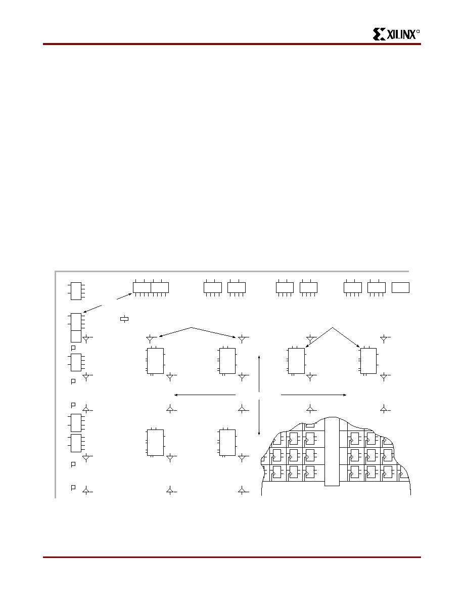
XC3100
XC3100A
(XC3195A)
Gate Capacity
X7068
Functionality
XC3000L
XC3000A
XC3100L
Speed
Figure 1: XC3000 FPGA Families
R
XC3000 Series Field Programmable Gate Arrays
7-6
November 9, 1998 (Version 3.1)
Detailed Functional Description
The perimeter of configurable Input/Output Blocks (IOBs)
provides a programmable interface between the internal
logic array and the device package pins. The array of Con-
figurable Logic Blocks (CLBs) performs user-specified logic
functions. The interconnect resources are programmed to
form networks, carrying logic signals among blocks, analo-
gous to printed circuit board traces connecting MSI/SSI
packages.
The block logic functions are implemented by programmed
look-up tables. Functional options are implemented by pro-
gram-controlled multiplexers. Interconnecting networks
between blocks are implemented with metal segments
joined by program-controlled pass transistors.
These FPGA functions are established by a configuration
program which is loaded into an internal, distributed array
of configuration memory cells. The configuration program
is loaded into the device at power-up and may be reloaded
on command. The FPGA includes logic and control signals
to implement automatic or passive configuration. Program
data may be either bit serial or byte parallel. The develop-
ment system generates the configuration program bit-
stream used to configure the device. The memory loading
process is independent of the user logic functions.
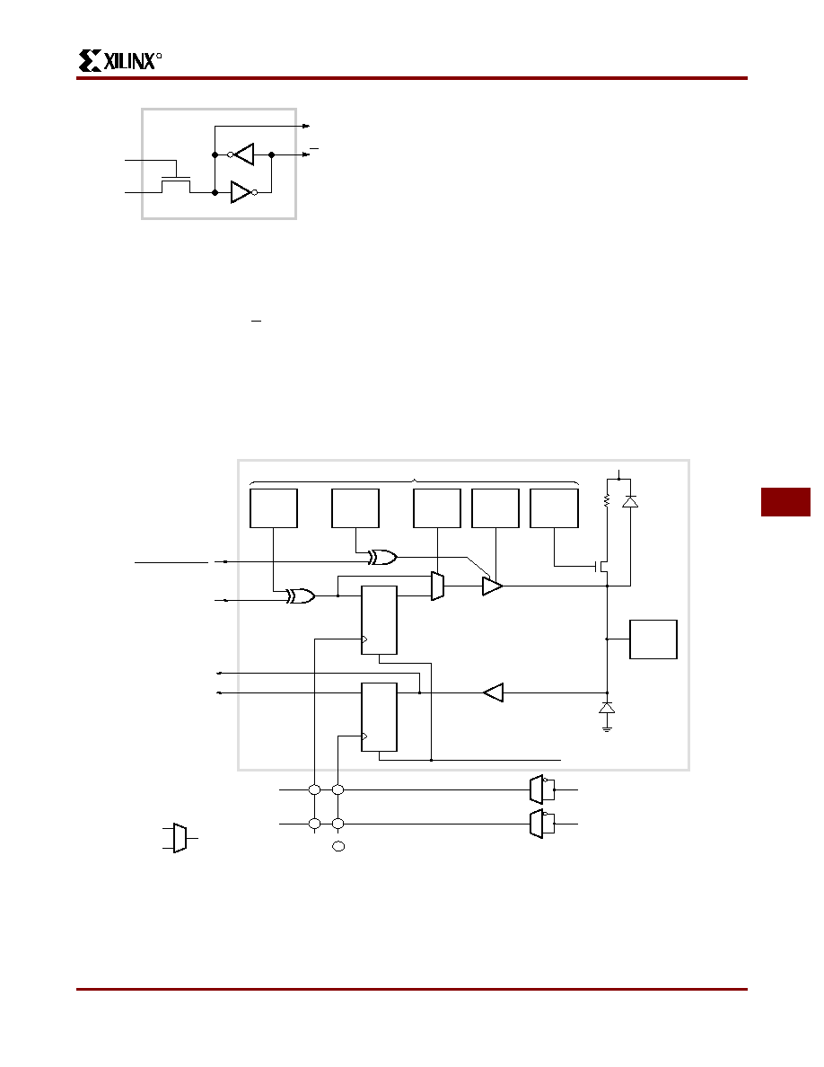
Configuration Memory
The static memory cell used for the configuration memory
in the Field Programmable Gate Array has been designed
specifically for high reliability and noise immunity. Integrity
of the device configuration memory based on this design is
assured even under adverse conditions. As shown in
Figure 3
, the basic memory cell consists of two CMOS
inverters plus a pass transistor used for writing and reading
cell data. The cell is only written during configuration and
only read during readback. During normal operation, the
cell provides continuous control and the pass transistor is
off and does not affect cell stability. This is quite different
from the operation of conventional memory devices, in
which the cells are frequently read and rewritten.
P9
P8
P7
P6
P5
P4
P3
P2
GND
PWR
DN
P11
P12
P13
U61
TCL
KIN
AD
AC
AB
AA
3-State Buffers With Access
to Horizontal Long Lines
Configurable Logic
Blocks
Interconnect Area
BB
BA
Frame Pointer
Configuration Memory
I/O Blocks
X3241
Figure 2: Field Programmable Gate Array Structure.
It consists of a perimeter of programmable I/O blocks, a core of configurable logic blocks and their interconnect resources.
These are all controlled by the distributed array of configuration program memory cells.
R
November 9, 1998 (Version 3.1)
7-7
XC3000 Series Field Programmable Gate Arrays
7
The memory cell outputs Q and Q use ground and V
CC
lev-
els and provide continuous, direct control. The additional
capacitive load together with the absence of address
decoding and sense amplifiers provide high stability to the
cell. Due to the structure of the configuration memory cells,
they are not affected by extreme power-supply excursions
or very high levels of alpha particle radiation. In reliability
testing, no soft errors have been observed even in the
presence of very high doses of alpha radiation.
The method of loading the configuration data is selectable.
Two methods use serial data, while three use byte-wide
data. The internal configuration logic utilizes framing infor-
mation, embedded in the program data by the development
system, to direct memory-cell loading. The serial-data
framing and length-count preamble provide programming
compatibility for mixes of various FPGA device devices in a
synchronous, serial, daisy-chain fashion.
I/O Block
Each user-configurable IOB shown in
Figure 4
, provides an
interface between the external package pin of the device
and the internal user logic. Each IOB includes both regis-
tered and direct input paths. Each IOB provides a program-
mable 3-state output buffer, which may be driven by a
registered or direct output signal. Configuration options
allow each IOB an inversion, a controlled slew rate and a
high impedance pull-up. Each input circuit also provides
input clamping diodes to provide electrostatic protection,
and circuits to inhibit latch-up produced by input currents.
Q
Data
Read or
Write
Configuration
Control
Q
X5382
Figure 3: Static Configuration Memory Cell.
It is loaded with one bit of configuration program and con-
trols one program selection in the Field Programmable
Gate Array.
FLIP
FLOP
Q
D
R
SLEW
RATE
PASSIVE
PULL UP
OUTPUT
SELECT
3-STATE
INVERT
OUT
INVERT
FLIP
FLOP
or
LATCH
D
Q
R
REGISTERED IN
DIRECT IN
OUT
3- STATE
(OUTPUT ENABLE)
TTL or
CMOS
INPUT
THRESHOLD
OUTPUT
BUFFER
(GLOBAL RESET)
CK1
X3029
I/O PAD
Vcc
PROGRAM-CONTROLLED MEMORY CELLS
PROGRAMMABLE INTERCONNECTION POINT or PIP
=
IK
OK
Q
I
O
T
PROGRAM
CONTROLLED
MULTIPLEXER
CK2
Figure 4: Input/Output Block.
Each IOB includes input and output storage elements and I/O options selected by configuration memory cells. A choice
of two clocks is available on each die edge. The polarity of each clock line (not each flip-flop or latch) is programmable.
A clock line that triggers the flip-flop on the rising edge is an active Low Latch Enable (Latch transparent) signal and vice
versa. Passive pull-up can only be enabled on inputs, not on outputs. All user inputs are programmed for TTL or CMOS
thresholds.

R
XC3000 Series Field Programmable Gate Arrays
7-8
November 9, 1998 (Version 3.1)
The input-buffer portion of each IOB provides threshold
detection to translate external signals applied to the pack-
age pin to internal logic levels. The global input-buffer
threshold of the IOBs can be programmed to be compatible
with either TTL or CMOS levels. The buffered input signal
drives the data input of a storage element, which may be
configured as either a flip-flop or a latch. The clocking
polarity (rising/falling edge-triggered flip-flop, High/Low
transparent latch) is programmable for each of the two
clock lines on each of the four die edges. Note that a clock
line driving a
rising edge-triggered flip-flop makes any latch
driven by the same line on the same edge Low-level trans-
parent and vice versa (
falling edge, High transparent). All
Xilinx primitives in the supported schematic-entry pack-
ages, however, are positive edge-triggered flip-flops or
High transparent latches. When one clock line must drive
flip-flops as well as latches, it is necessary to compensate
for the difference in clocking polarities with an additional
inverter either in the flip-flop clock input or the latch-enable
input. I/O storage elements are reset during configuration
or by the active-Low chip RESET input. Both direct input
(from IOB pin I) and registered input (from IOB pin Q) sig-
nals are available for interconnect.
For reliable operation, inputs should have transition times
of less than 100 ns and should not be left floating. Floating
CMOS input-pin circuits might be at threshold and produce
oscillations. This can produce additional power dissipation
and system noise. A typical hysteresis of about 300 mV
reduces sensitivity to input noise. Each user IOB includes a
programmable high-impedance pull-up resistor, which may
be selected by the program to provide a constant High for
otherwise undriven package pins. Although the Field Pro-
grammable Gate Array provides circuitry to provide input
protection for electrostatic discharge, normal CMOS han-
dling precautions should be observed.
Flip-flop loop delays for the IOB and logic-block flip-flops
are short, providing good performance under asynchro-
nous clock and data conditions. Short loop delays minimize
the probability of a metastable condition that can result
from assertion of the clock during data transitions. Because
of the short-loop-delay characteristic in the Field Program-
mable Gate Array, the IOB flip-flops can be used to syn-
chronize external signals applied to the device. Once
synchronized in the IOB, the signals can be used internally
without further consideration of their clock relative timing,
except as it applies to the internal logic and routing-path
delays.
IOB output buffers provide CMOS-compatible 4-mA
source-or-sink drive for high fan-out CMOS or TTL- com-
patible signal levels (8 mA in the XC3100A family). The net-
work driving IOB pin O becomes the registered or direct
data source for the output buffer. The 3-state control signal
(IOB) pin T can control output activity. An open-drain output
may be obtained by using the same signal for driving the
output and 3-state signal nets so that the buffer output is
enabled only for a Low.
Configuration program bits for each IOB control features
such as optional output register, logic signal inversion, and
3-state and slew-rate control of the output.
The program-controlled memory cells of
Figure 4
control
the following options.
�
Logic inversion of the output is controlled by one
configuration program bit per IOB.
�
Logic 3-state control of each IOB output buffer is
determined by the states of configuration program bits
that turn the buffer on, or off, or select the output buffer
3-state control interconnection (IOB pin T). When this
IOB output control signal is High, a logic one, the buffer
is disabled and the package pin is high impedance.
When this IOB output control signal is Low, a logic zero,
the buffer is enabled and the package pin is active.
Inversion of the buffer 3-state control-logic sense
(output enable) is controlled by an additional
configuration program bit.
�
Direct or registered output is selectable for each IOB.
The register uses a positive-edge, clocked flip-flop. The
clock source may be supplied (IOB pin OK) by either of
two metal lines available along each die edge. Each of
these lines is driven by an invertible buffer.
�
Increased output transition speed can be selected to
improve critical timing. Slower transitions reduce
capacitive-load peak currents of non-critical outputs
and minimize system noise.
�
An internal high-impedance pull-up resistor (active by
default) prevents unconnected inputs from floating.
Unlike the original XC3000 series, the XC3000A,
XC3000L, XC3100A, and XC3100L families include the
Soft Startup feature. When the configuration process is fin-
ished and the device starts up in user mode, the first activa-
tion of the outputs is automatically slew-rate limited. This
feature avoids potential ground bounce when all outputs
are turned on simultaneously. After start-up, the slew rate
of the individual outputs is determined by the individual
configuration option.
Summary of I/O Options
�
Inputs
-
Direct
-
Flip-flop/latch
-
CMOS/TTL threshold (chip inputs)
-
Pull-up resistor/open circuit
�
Outputs
-
Direct/registered
-
Inverted/not
-
3-state/on/off
-
Full speed/slew limited
-
3-state/output enable (inverse)
R
November 9, 1998 (Version 3.1)
7-9
XC3000 Series Field Programmable Gate Arrays
7
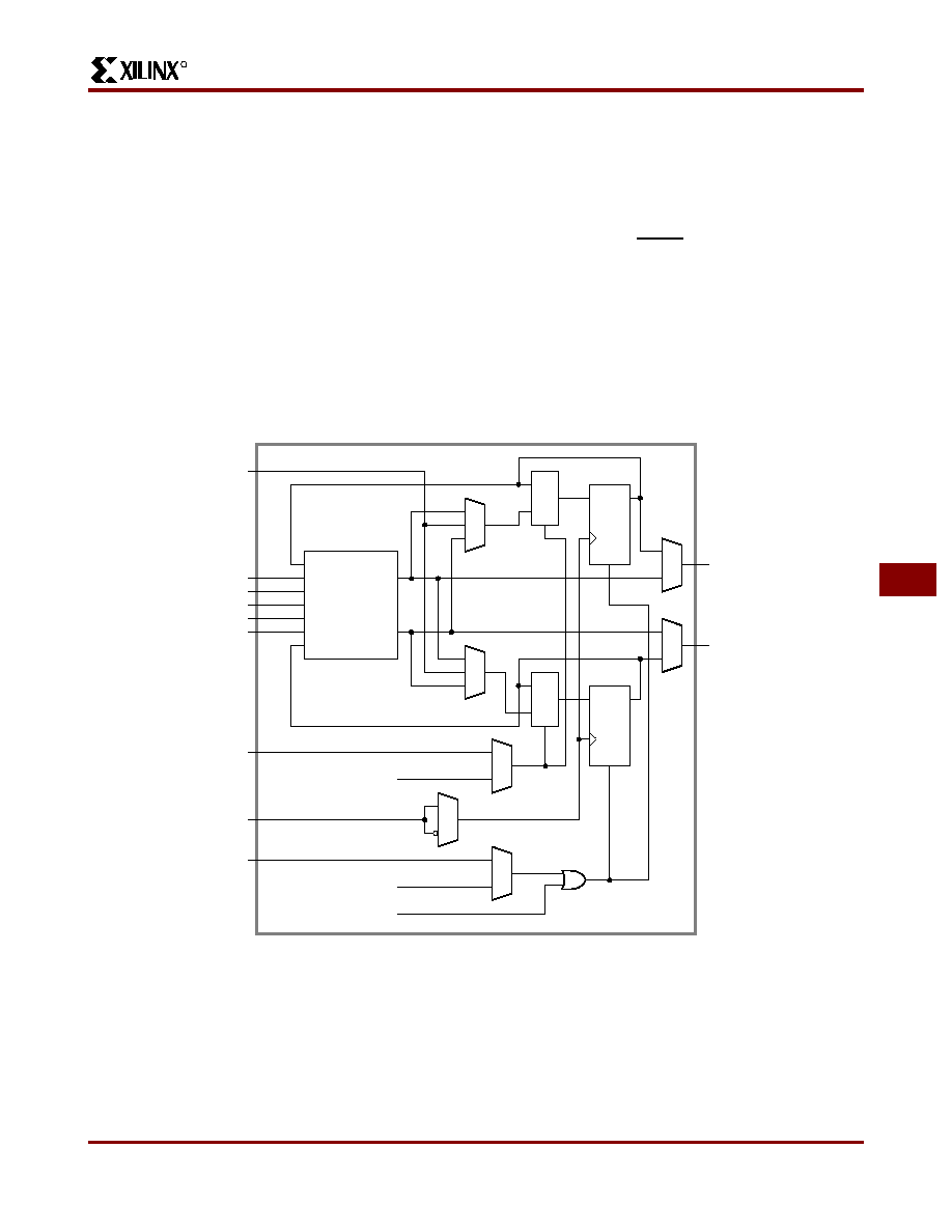
Configurable Logic Block
The array of CLBs provides the functional elements from
which the user's logic is constructed. The logic blocks are
arranged in a matrix within the perimeter of IOBs. For
example, the XC3020A has 64 such blocks arranged in 8
rows and 8 columns. The development system is used to
compile the configuration data which is to be loaded into
the internal configuration memory to define the operation
and interconnection of each block. User definition of CLBs
and their interconnecting networks may be done by auto-
matic translation from a schematic-capture logic diagram or
optionally by installing library or user macros.
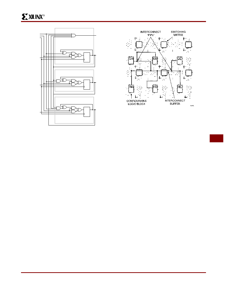
Each CLB has a combinatorial logic section, two flip-flops,
and an internal control section. See
Figure 5
. There are:
five logic inputs (A, B, C, D and E); a common clock input
(K); an asynchronous direct RESET input (RD); and an
enable clock (EC). All may be driven from the interconnect
resources adjacent to the blocks. Each CLB also has two
outputs (X and Y) which may drive interconnect networks.
Data input for either flip-flop within a CLB is supplied from
the function F or G outputs of the combinatorial logic, or the
block input, DI. Both flip-flops in each CLB share the asyn-
chronous RD which, when enabled and High, is dominant
over clocked inputs. All flip-flops are reset by the
active-Low chip input, RESET, or during the configuration
process. The flip-flops share the enable clock (EC) which,
when Low, recirculates the flip-flops' present states and
inhibits response to the data-in or combinatorial function
inputs on a CLB. The user may enable these control inputs
and select their sources. The user may also select the
clock net input (K), as well as its active sense within each
CLB. This programmable inversion eliminates the need to
route both phases of a clock signal throughout the device.
Q
COMBINATORIAL
FUNCTION
LOGIC
VARIABLES
D
RD
G
F
DIN
F
G
QX
QY
DIN
F
G
G
QY
QX
F
Q
D
RD
ENABLE CLOCK
CLOCK
DIRECT
RESET
1 (ENABLE)
A
B
C
D
E
DI
EC
K
RD
Y
X
X3032
0 (INHIBIT)
(GLOBAL RESET)
CLB OUTPUTS
DATA IN
0
1
0
1
MUX
MUX
Figure 5: Configurable Logic Block.
Each CLB includes a combinatorial logic section, two flip-flops and a program memory controlled multiplexer selection of
function. It has the following:
-
five logic variable inputs A, B, C, D, and E
-
a direct data in DI
-
an enable clock EC
-
a clock (invertible) K
-
an asynchronous direct RESET RD
-
two outputs X and Y
R
XC3000 Series Field Programmable Gate Arrays
7-10
November 9, 1998 (Version 3.1)
Flexible routing allows use of common or individual CLB
clocking.
The combinatorial-logic portion of the CLB uses a 32 by 1
look-up table to implement Boolean functions. Variables
selected from the five logic inputs and two internal block
flip-flops are used as table address inputs. The combinato-
rial propagation delay through the network is independent
of the logic function generated and is spike free for single
input variable changes. This technique can generate two
independent logic functions of up to four variables each as
shown in Figure 6a, or a single function of five variables as
shown in Figure 6b, or some functions of seven variables
as shown in Figure 6c.
Figure 7
shows a modulo-8 binary
counter with parallel enable. It uses one CLB of each type.
The partial functions of six or seven variables are imple-
mented using the input variable (E) to dynamically select
between two functions of four different variables. For the
two functions of four variables each, the independent
results (F and G) may be used as data inputs to either
flip-flop or either logic block output. For the single function
of five variables and merged functions of six or seven vari-
ables, the F and G outputs are identical. Symmetry of the F
and G functions and the flip-flops allows the interchange of
CLB outputs to optimize routing efficiencies of the networks
interconnecting the CLBs and IOBs.
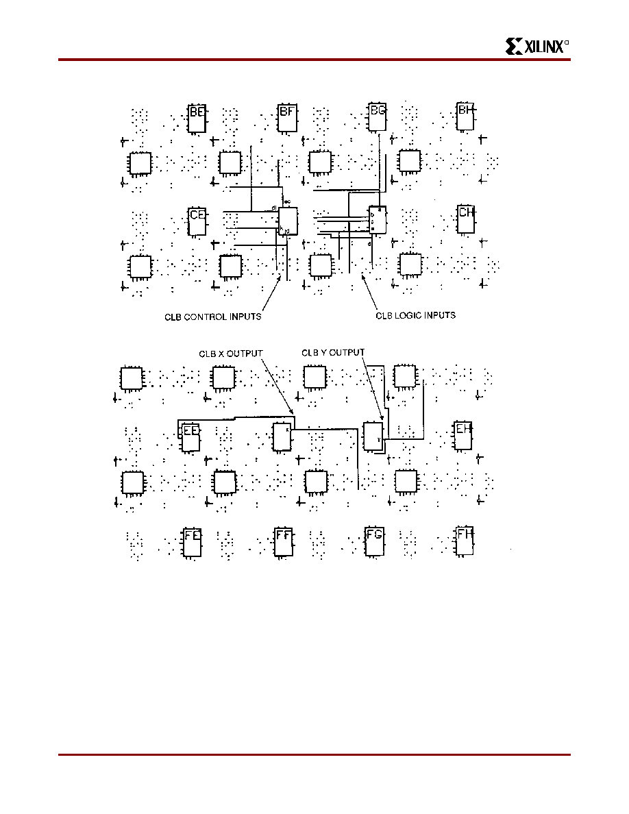
Programmable Interconnect
Programmable-interconnection resources in the Field Pro-
grammable Gate Array provide routing paths to connect
inputs and outputs of the IOBs and CLBs into logic net-
works. Interconnections between blocks are composed of a
two-layer grid of metal segments. Specially designed pass
transistors, each controlled by a configuration bit, form pro-
grammable interconnect points (PIPs) and switching matri-
ces used to implement the necessary connections between
selected metal segments and block pins.
Figure 8
is an
example of a routed net. The development system provides
automatic routing of these interconnections. Interactive
routing is also available for design optimization. The inputs
of the CLBs or IOBs are multiplexers which can be pro-
grammed to select an input network from the adjacent
interconnect segments.
Since the switch connections to
block inputs are unidirectional, as are block outputs,
they are usable only for block input connection and not
for routing.
Figure 9
illustrates routing access to logic
block input variables, control inputs and block outputs.
Three types of metal resources are provided to accommo-
date various network interconnect requirements.
�
General Purpose Interconnect
�
Direct Connection
�
Longlines (multiplexed busses and wide AND gates)
QY
Any Function
of Up to 4
Variables
QY
Any Function
of Up to 4
Variables
QY
Any Function
of 5 Variables
QY
Any Function
of Up to 4
Variables
QY
Any Function
of Up to 4
Variables
5c
5b
5a
QX
QX
QX
QX
QX
A
B
C
D
A
B
C
D
E
E
A
B
C
D
E
D
A
B
C
D
C
A
B
M
U
X
F
G
F
G
F
G
E
X5442
FGM
Mode
Figure 6: Combinational Logic Options
6a. Combinatorial Logic Option FG generates two func-
tions of four variables each. One variable, A, must be
common to both functions. The second and third variable
can be any choice of B, C, QX and QY. The fourth vari-
able can be any choice of D or E.
6b. Combinatorial Logic Option F generates any function
of five variables: A, D, E and two choices out of B, C, QX,
QY.
6c. Combinatorial Logic Option FGM allows variable E to
select between two functions of four variables: Both have
common inputs A and D and any choice out of B, C, QX
and QY for the remaining two variables. Option 3 can
then implement some functions of six or seven variables.
R
November 9, 1998 (Version 3.1)
7-11
XC3000 Series Field Programmable Gate Arrays
7
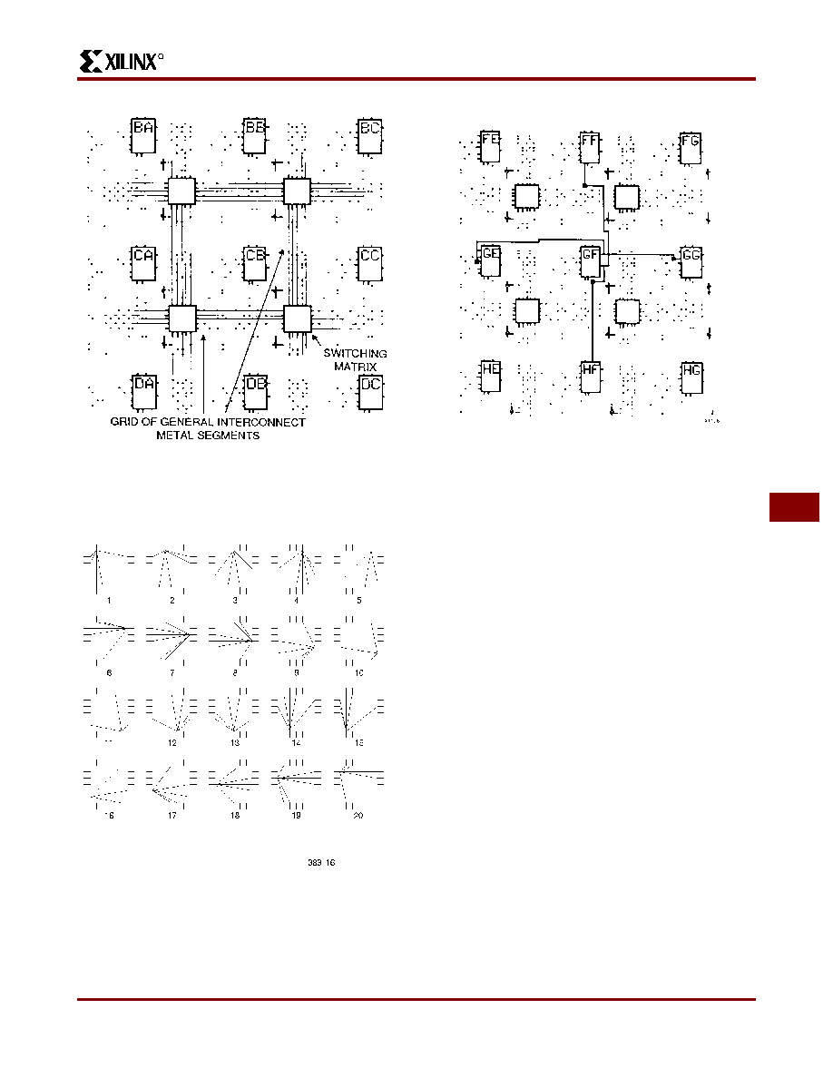
General Purpose Interconnect
General purpose interconnect, as shown in
Figure 10
, con-
sists of a grid of five horizontal and five vertical metal seg-
ments located between the rows and columns of logic and
IOBs. Each segment is the height or width of a logic block.
Switching matrices join the ends of these segments and
allow programmed interconnections between the metal grid
segments of adjoining rows and columns. The switches of
an unprogrammed device are all non-conducting. The con-
nections through the switch matrix may be established by
the automatic routing or by selecting the desired pairs of
matrix pins to be connected or disconnected. The legiti-
mate switching matrix combinations for each pin are indi-
cated in
Figure 11
.
Special buffers within the general interconnect areas pro-
vide periodic signal isolation and restoration for improved
performance of lengthy nets. The interconnect buffers are
available to propagate signals in either direction on a given
general interconnect segment. These bidirectional (bidi)
buffers are found adjacent to the switching matrices, above
and to the right. The other PIPs adjacent to the matrices
are accessed to or from Longlines. The development sys-
tem automatically defines the buffer direction based on the
location of the interconnection network source. The delay
calculator of the development system automatically calcu-
lates and displays the block, interconnect and buffer delays
for any paths selected. Generation of the simulation netlist
with a worst-case delay model is provided.
Direct Interconnect
Direct interconnect, shown in
Figure 12
, provides the most
efficient implementation of networks between adjacent
CLBs or I/O Blocks. Signals routed from block to block
using the direct interconnect exhibit minimum interconnect
propagation and use no general interconnect resources.
For each CLB, the X output may be connected directly to
the B input of the CLB immediately to its right and to the C
input of the CLB to its left. The Y output can use direct inter-
connect to drive the D input of the block immediately above
and the A input of the block below. Direct interconnect
should be used to maximize the speed of high-performance
portions of logic. Where logic blocks are adjacent to IOBs,
direct connect is provided alternately to the IOB inputs (I)
and outputs (O) on all four edges of the die. The right edge
provides additional direct connects from CLB outputs to
adjacent IOBs. Direct interconnections of IOBs with CLBs
are shown in
Figure 13
.
D
Q
D
Q
D
Q
Count Enable
Parallel Enable
Clock
D2
D1
D0
Dual Function of 4 Variables
Function of 6 Variables
Function of 5 Variables
Q2
Q1
Q0
FG
Mode
F
Mode
FGM
Mode
Terminal
Count
X5383
Figure 7: Counter.
The modulo-8 binary counter with parallel enable and
clock enable uses one combinatorial logic block of each
option.
Figure 8: A Design Editor view of routing resources
used to form a typical interconnection network from
CLB GA.
R
XC3000 Series Field Programmable Gate Arrays
7-12
November 9, 1998 (Version 3.1)
Figure 9: Design Editor Locations of interconnect access, CLB control inputs, logic inputs and outputs. The dot pattern
represents the available programmable interconnection points (PIPs).
Some of the interconnect PIPs are directional.
R
November 9, 1998 (Version 3.1)
7-13
XC3000 Series Field Programmable Gate Arrays
7
Figure 10: FPGA General-Purpose Interconnect.
Composed of a grid of metal segments that may be inter-
connected through switch matrices to form networks for
CLB and IOB inputs and outputs.
Figure 11: Switch Matrix Interconnection Options for
Each Pin.
Switch matrices on the edges are different.
Figure 12: CLB X and Y Outputs.
The X and Y outputs of each CLB have single contact,
direct access to inputs of adjacent CLBs

R
XC3000 Series Field Programmable Gate Arrays
7-14
November 9, 1998 (Version 3.1)
Figure 13: XC3020A Die-Edge IOBs. The XC3020A die-edge IOBs are provided with direct access to adjacent CLBs.
Global Buffer Direct Input
Global Buffer Inerconnect
Alternate Buffer Direct Input
* Unbonded IOBs (6 Places)

R
November 9, 1998 (Version 3.1)
7-15
XC3000 Series Field Programmable Gate Arrays
7
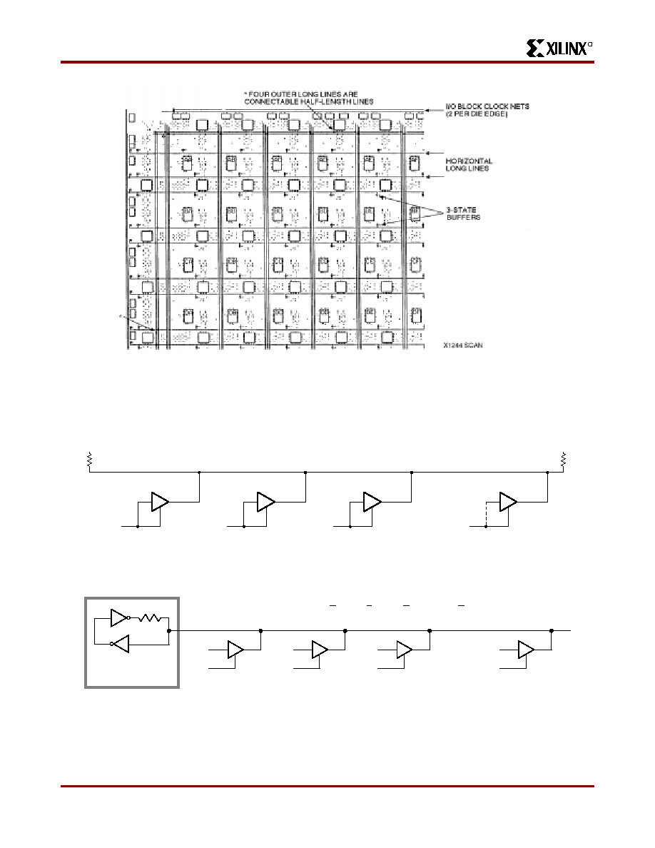
Longlines
The Longlines bypass the switch matrices and are intended
primarily for signals that must travel a long distance, or
must have minimum skew among multiple destinations.
Longlines, shown in
Figure 14
, run vertically and horizon-
tally the height or width of the interconnect area. Each inter-
connection column has three vertical Longlines, and each
interconnection row has two horizontal Longlines. Two
additional Longlines are located adjacent to the outer sets
of switching matrices. In devices larger than the XC3020A
and XC3120A FPGAs, two vertical Longlines in each col-
umn are connectable half-length lines. On the XC3020A
and XC3120A FPGAs, only the outer Longlines are con-
nectable half-length lines.
Longlines can be driven by a logic block or IOB output on a
column-by-column basis. This capability provides a com-
mon low skew control or clock line within each column of
logic blocks. Interconnections of these Longlines are
shown in
Figure 15
. Isolation buffers are provided at each
input to a Longline and are enabled automatically by the
development system when a connection is made.
Figure 14: Horizontal and Vertical Longlines. These Longlines provide high fan-out, low-skew signal distribution in
each row and column. The global buffer in the upper left die corner drives a common line throughout the FPGA.
R
XC3000 Series Field Programmable Gate Arrays
7-16
November 9, 1998 (Version 3.1)
Figure 15: Programmable Interconnection of Longlines. This is provided at the edges of the routing area.
Three-state buffers allow the use of horizontal Longlines to form on-chip wired AND and multiplexed buses. The left two
non-clock vertical Longlines per column (except XC3020A) and the outer perimeter Longlines may be programmed as
connectable half-length lines.
V
CC
D
A
D
B
D
C
D
N
V
CC
Z
=
D
A
�
D
B
�
D
C
�
...
�
D
N
X3036
(LOW)
Figure 16: 3-State Buffers Implement a Wired-AND Function. When all the buffer 3-state lines are High, (high
impedance), the pull-up resistor(s) provide the High output. The buffer inputs are driven by the control signals or a Low.
D
A
A
D
B
B
D
C
C
D
N
N
D
A
A
�
+
=
D
B
B
�
+ D
C
C
�
+
D
N
N
�
Z
... +
X1741A
WEAK
KEEPER CIRCUIT
Figure 17: 3-State Buffers Implement a Multiplexer. The selection is accomplished by the buffer 3-state signal.

R
November 9, 1998 (Version 3.1)
7-17
XC3000 Series Field Programmable Gate Arrays
7
A buffer in the upper left corner of the FPGA chip drives a
global net which is available to all K inputs of logic blocks.
Using the global buffer for a clock signal provides a
skew-free, high fan-out, synchronized clock for use at any
or all of the IOBs and CLBs. Configuration bits for the K
input to each logic block can select this global line or
another routing resource as the clock source for its
flip-flops. This net may also be programmed to drive the die
edge clock lines for IOB use. An enhanced speed, CMOS
threshold, direct access to this buffer is available at the sec-
ond pad from the top of the left die edge.
A buffer in the lower right corner of the array drives a hori-
zontal Longline that can drive programmed connections to
a vertical Longline in each interconnection column. This
alternate buffer also has low skew and high fan-out. The
network formed by this alternate buffer's Longlines can be
selected to drive the K inputs of the CLBs. CMOS thresh-
old, high speed access to this buffer is available from the
third pad from the bottom of the right die edge.
Internal Busses
A pair of 3-state buffers, located adjacent to each CLB, per-
mits logic to drive the horizontal Longlines. Logic operation
of the 3-state buffer controls allows them to implement wide
multiplexing functions. Any 3-state buffer input can be
selected as drive for the horizontal long-line bus by apply-
ing a Low logic level on its 3-state control line. See
Figure 16
. The user is required to avoid contention which
can result from multiple drivers with opposing logic levels.
Control of the 3-state input by the same signal that drives
the buffer input, creates an open-drain wired-AND function.
A logic High on both buffer inputs creates a high imped-
ance, which represents no contention. A logic Low enables
the buffer to drive the Longline Low. See
Figure 17
. Pull-up
resistors are available at each end of the Longline to pro-
vide a High output when all connected buffers are non-con-
ducting. This forms fast, wide gating functions. When data
drives the inputs, and separate signals drive the 3-state
control lines, these buffers form multiplexers (3-state bus-
ses). In this case, care must be used to prevent contention
through multiple active buffers of conflicting levels on a
common line. Each horizontal Longline is also driven by a
weak keeper circuit that prevents undefined floating levels
by maintaining the previous logic level when the line is not
driven by an active buffer or a pull-up resistor.
Figure 18
shows 3-state buffers, Longlines and pull-up resistors.
3-STATE CONTROL
GG
HG
P40
P41
P42
P43
RST
P46
.l
X1245
.q
.Q
OS
C
P47
BCL
KIN
P48
GH
HH
.lk
.ck
I/O CLOCKS
BIDIRECTIONAL
INTERCONNECT
BUFFERS
GLOBAL NET
3 VERTICAL LONG
LINES PER COLUMN
HORIZONTAL LONG LINE
PULL-UP RESISTOR
HORIZONTAL LONG LINE
OSCILLATOR
AMPLIFIER OUTPUT
DIRECTINPUT OF P47
TO AUXILIARY BUFFER
CRYSTAL OSCILLATOR
BUFFER
3-STATE INPUT
3-STATE BUFFER
ALTERNATE BUFFER
D
P
G
M
Figure 18: Design Editor.
An extra large view of possible interconnections in the lower right corner of the XC3020A.

R
XC3000 Series Field Programmable Gate Arrays
7-18
November 9, 1998 (Version 3.1)
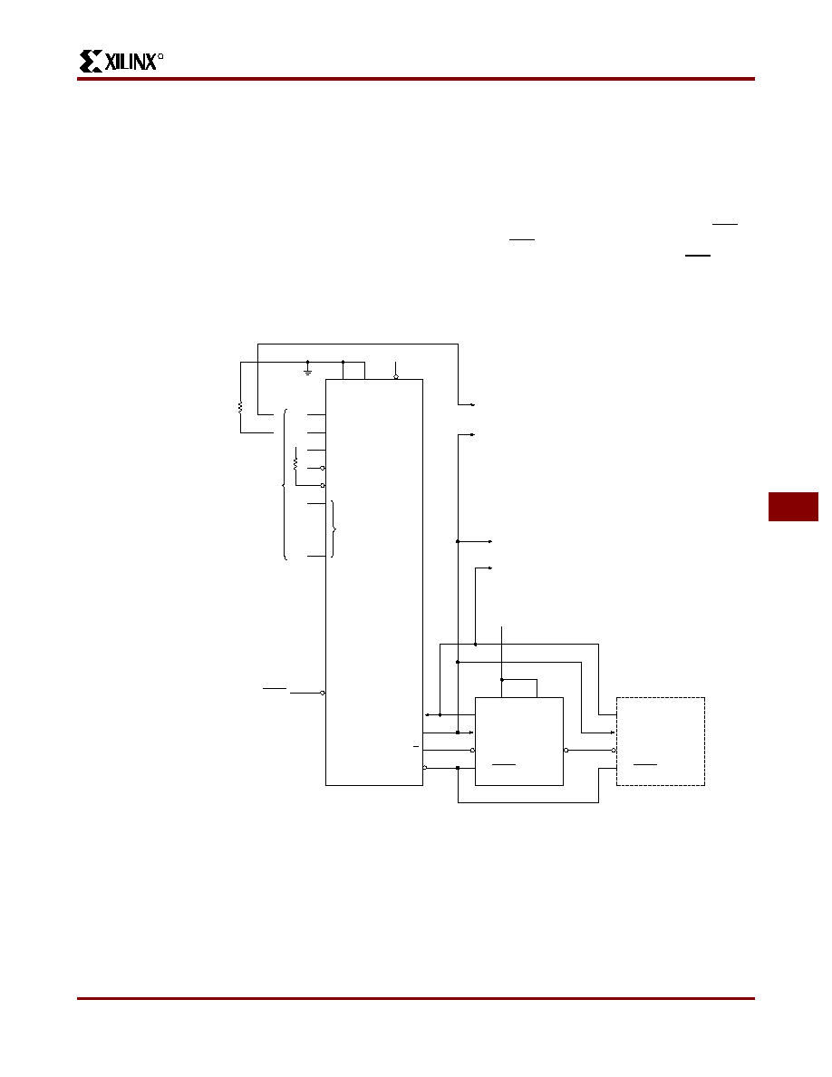
Crystal Oscillator
Figure 18
also shows the location of an internal high speed
inverting amplifier that may be used to implement an
on-chip crystal oscillator. It is associated with the auxiliary
buffer in the lower right corner of the die. When the oscilla-
tor is configured and connected as a signal source, two
special user IOBs are also configured to connect the oscil-
lator amplifier with external crystal oscillator components
as shown in
Figure 19
. A divide by two option is available to
assure symmetry. The oscillator circuit becomes active
early in the configuration process to allow the oscillator to
stabilize. Actual internal connection is delayed until com-
pletion of configuration. In
Figure 19
the feedback resistor
R1, between the output and input, biases the amplifier at
threshold. The inversion of the amplifier, together with the
R-C networks and an AT-cut series resonant crystal, pro-
duce the 360-degree phase shift of the Pierce oscillator. A
series resistor R2 may be included to add to the amplifier
output impedance when needed for phase-shift control,
crystal resistance matching, or to limit the amplifier input
swing to control clipping at large amplitudes. Excess feed-
back voltage may be corrected by the ratio of C2/C1. The
amplifier is designed to be used from 1 MHz to about
one-half the specified CLB toggle frequency. Use at fre-
quencies below 1 MHz may require individual characteriza-
tion with respect to a series resistance. Crystal oscillators
above 20 MHz generally require a crystal which operates in
a third overtone mode, where the fundamental frequency
must be suppressed by an inductor across C2, turning this
parallel resonant circuit to double the fundamental crystal
frequency, i.e., 2/3 of the desired third harmonic frequency
network. When the oscillator inverter is not used, these
IOBs and their package pins are available for general user
I/O.
Alternate
Clock Buffer
XTAL1
XTAL2
(IN)
R1
R2
Y1
C1
C2
Internal
External
R1
R2
C1, C2
Y1
Suggested Component Values
0.5 � 1 M
0 � 1 k
(may be required for low frequency, phase
shift and/or compensation level for crystal Q)
10 � 40 pF
1 � 20 MHz AT-cut parallel resonant
X7064
68 PIN
PLCC
47
43
84 PIN
PLCC
57
53
PGA
J11
L11
132 PIN
PGA
P13
M13
160 PIN
PQFP
82
76
XTAL 1 (OUT)
XTAL 2 (IN)
100 PIN
CQFP
67
61
PQFP
82
76
164 PIN
CQFP
105
99
44 PIN
PLCC
30
26
175 PIN
PGA
T14
P15
208 PIN
PQFP
110
100
176 PIN
TQFP
91
85
D
Q
Figure 19: Crystal Oscillator Inverter. When activated, and by selecting an output network for its buffer, the crystal
oscillator inverter uses two unconfigured package pins and external components to implement an oscillator. An optional
divide-by-two mode is available to assure symmetry.

R
November 9, 1998 (Version 3.1)
7-19
XC3000 Series Field Programmable Gate Arrays
7
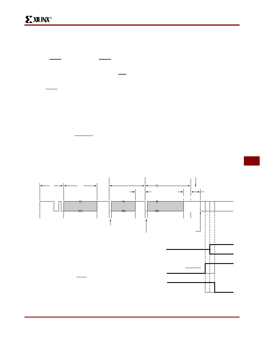
Configuration
Initialization Phase
An internal power-on-reset circuit is triggered when power
is applied. When V
CC
reaches the voltage at which portions
of the FPGA device begin to operate (nominally 2.5 to 3 V),
the programmable I/O output buffers are 3-stated and a
high-impedance pull-up resistor is provided for the user
I/O pins. A time-out delay is initiated to allow the power
supply voltage to stabilize. During this time the power-down
mode is inhibited. The Initialization state time-out (about 11
to 33 ms) is determined by a 14-bit counter driven by a
self-generated internal timer. This nominal 1-MHz timer is
subject to variations with process, temperature and power
supply. As shown in
Table 1
, five configuration mode
choices are available as determined by the input levels of
three mode pins; M0, M1 and M2.
In Master configuration modes, the device becomes the
source of the Configuration Clock (CCLK). The beginning
of configuration of devices using Peripheral or Slave
modes must be delayed long enough for their initialization
to be completed. An FPGA with mode lines selecting a
Master configuration mode extends its initialization state
using four times the delay (43 to 130 ms) to assure that all
daisy-chained slave devices, which it may be driving, will
be ready even if the master is very fast, and the slave(s)
very slow.
Figure 20
shows the state sequences. At the end
of Initialization, the device enters the Clear state where it
clears the configuration memory. The active Low,
open-drain initialization signal INIT indicates when the Ini-
tialization and Clear states are complete. The FPGA tests
for the absence of an external active Low RESET before it
makes a final sample of the mode lines and enters the Con-
figuration state. An external wired-AND of one or more INIT
pins can be used to control configuration by the assertion of
the active-Low RESET of a master mode device or to sig-
nal a processor that the FPGAs are not yet initialized.
If a configuration has begun, a re-assertion of RESET for a
minimum of three internal timer cycles will be recognized
and the FPGA will initiate an abort, returning to the Clear
state to clear the partially loaded configuration memory
words. The FPGA will then resample RESET and the mode
lines before re-entering the Configuration state.
During configuration, the XC3000A, XC3000L, XC3100A,
and XC3100L devices check the bit-stream format for stop
bits in the appropriate positions. Any error terminates the
configuration and pulls INIT Low.
Table 1: Configuration Mode Choices
M0 M1 M2
CCLK
Mode
Data
0
0
0
output
Master
Bit Serial
0
0
1
output
Master
Byte Wide Addr. = 0000 up
0
1
0
--
reserved
--
0
1
1
output
Master
Byte Wide Addr. = FFFF down
1
0
0
--
reserved
--
1
0
1
output
Peripheral Byte Wide
1
1
0
--
reserved
--
1
1
1
input
Slave
Bit Serial
All User I/O Pins 3-Stated with High Impedance Pull-Up, HDC=High, LDC=Low
Initialization
Power-On
Time Delay
Clear
Configuration
Memory
Test
Mode Pins
Configuration
Program Mode
Start-Up
Operational
Mode
Power Down
No HDC, LDC
or Pull-Up
No
X3399
INIT Output = Low
Clear Is
~ 200 Cycles for the XC3020A--130 to 400
�
s
~ 250 Cycles for the XC3030A--165 to 500
�
s
~ 290 Cycles for the XC3042A--195 to 580
�
s
~ 330 Cycles for the XC3064A--220 to 660
�
s
~ 375 Cycles for the XC3090A--250 to 750
�
s
RESET
Active
PWRDWN
Inactive
PWRDWN
Active
Active RESET
Operates on
User Logic
Low on DONE/PROGRAM and RESET
Active RESET
Power-On Delay is
2
14
Cycles for Non-Master Mode--11 to 33 ms
2
16
Cycles for Master Mode--43 to 130 ms
Figure 20: A State Diagram of the Configuration Process for Power-up and Reprogram.

R
XC3000 Series Field Programmable Gate Arrays
7-20
November 9, 1998 (Version 3.1)
A re-program is initiated.when a configured XC3000 series
device senses a High-to-Low transition and subsequent >6
�
s Low level on the DONE/PROG package pin, or, if this
pin is externally held permanently Low, a High-to-Low tran-
sition and subsequent >6
�
s Low time on the RESET pack-
age pin.
The device returns to the Clear state where the configura-
tion memory is cleared and mode lines re-sampled, as for
an aborted configuration. The complete configuration pro-
gram is cleared and loaded during each configuration pro-
gram cycle.
Length count control allows a system of multiple Field Pro-
grammable Gate Arrays, of assorted sizes, to begin opera-
tion in a synchronized fashion. The configuration program
generated by the development system begins with a pre-
amble of 111111110010 followed by a 24-bit length count
representing the total number of configuration clocks
needed to complete loading of the configuration pro-
gram(s). The data framing is shown in
Figure 21
. All
FPGAs connected in series read and shift preamble and
length count in on positive and out on negative configura-
tion clock edges. A device which has received the pream-
ble and length count then presents a High Data Out until it
has intercepted the appropriate number of data frames.
When the configuration program memory of an FPGA is full
and the length count does not yet compare, the device
shifts any additional data through, as it did for preamble
and length count. When the FPGA configuration memory is
full and the length count compares, the device will execute
11111111
0010
< 24-Bit Length Count >
1111
0 <Data Frame # 001 > 111
0 <Data Frame # 002 > 111
0 <Data Frame # 003 > 111
. . .
. . .
. . .
0 <Data Frame # 196 > 111
0 <Data Frame # 197 > 111
1111
--Dummy Bits*
--Preamble Code
--Configuration Program Length
--Dummy Bits (4 Bits Minimum)
For XC3120
197 Configuration Data Frames
(Each Frame Consists of:
A Start Bit (0)
A 71-Bit Data Field
Three Stop Bits
Postamble Code (4 Bits Minimum)
Header
Program Data
Repeated for Each Logic
Cell Array in a Daisy Chain
*The LCA Device Require Four Dummy Bits Min; Software Generates Eight Dummy Bits
X5300_01
Figure 21: Internal Configuration Data Structure for an FPGA. This shows the preamble, length count and data
frames generated by the Development System.
The Length Count produced by the program = [(40-bit preamble + sum of program data + 1 per daisy chain device)
rounded up to multiple of 8] � (2
K
4) where K is a function of DONE and RESET timing selected. An additional 8 is
added if roundup increment is less than K. K additional clocks are needed to complete start-up after length count is
reached.
Device
XC3020A
XC3020L
XC3120A
XC3030A
XC3030L
XC3130A
XC3042A
XC3042L
XC3142A
XC3142L
XC3064A
XC3064L
XC3164A
XC3090A
XC3090L
XC3190A
XC3190L
XC3195A
Gates
1,000 to 1,500
1,500 to 2,000
2,000 to 3,000
3,500 to 4,500
5,000 to 6,000
6,500 to 7,500
CLBs
64
100
144
224
320
484
Row x Col
(8 x 8)
(10 x 10)
(12 x 12)
(16 x 14)
(20 x 16)
(22 x 22)
IOBs
64
80
96
120
144
176
Flip-flops
256
360
480
688
928
1,320
Horizontal Longlines
16
20
24
32
40
44
TBUFs/Horizontal LL
9
11
13
15
17
23
Bits per Frame
(including1 start and 3 stop bits)
75
92
108
140
172
188
Frames
197
241
285
329
373 505
Program Data =
Bits x Frames + 4 bits
(excludes header)
14,779
22,176
30,784
46,064
64,160
94,944
PROM size (bits) =
Program Data
+ 40-bit Header
14,819
22,216
30,824
46,104
64,200
94,984
R
November 9, 1998 (Version 3.1)
7-21
XC3000 Series Field Programmable Gate Arrays
7
a synchronous start-up sequence and become operational.
See
Figure 22
. Two CCLK cycles after the completion of
loading configuration data, the user I/O pins are enabled as
configured. As selected, the internal user-logic RESET is
released either one clock cycle before or after the I/O pins
become active. A similar timing selection is programmable
for the DONE/PROG output signal. DONE/PROG may also
be programmed to be an open drain or include a pull-up
resistor to accommodate wired ANDing. The High During
Configuration (HDC) and Low During Configuration (LDC)
are two user I/O pins which are driven active while an
FPGA is in its Initialization, Clear or Configure states. They
and DONE/PROG provide signals for control of external
logic signals such as RESET, bus enable or PROM enable
during configuration. For parallel Master configuration
modes, these signals provide PROM enable control and
allow the data pins to be shared with user logic signals.
User I/O inputs can be programmed to be either TTL or
CMOS compatible thresholds. At power-up, all inputs have
TTL thresholds and can change to CMOS thresholds at the
completion of configuration if the user has selected CMOS
thresholds. The threshold of PWRDWN and the direct clock
inputs are fixed at a CMOS level.
If the crystal oscillator is used, it will begin operation before
configuration is complete to allow time for stabilization
before it is connected to the internal circuitry.
Configuration Data
Configuration data to define the function and interconnec-
tion within a Field Programmable Gate Array is loaded from
an external storage at power-up and after a re-program sig-
nal. Several methods of automatic and controlled loading of
the required data are available. Logic levels applied to
mode selection pins at the start of configuration time deter-
mine the method to be used. See Table 1. The data may be
either bit-serial or byte-parallel, depending on the configu-
ration mode. The different FPGAs have different sizes and
numbers of data frames. To maintain compatibility between
various device types, the Xilinx product families use com-
patible configuration formats. For the XC3020A, configura-
tion requires 14779 bits for each device, arranged in 197
data frames. An additional 40 bits are used in the header.
See
Figure 22
. The specific data format for each device is
produced by the development system and one or more of
these files can then be combined and appended to a length
count preamble and be transformed into a PROM format
file by the development system. A compatibility exception
precludes the use of an XC2000-series device as the mas-
ter for XC3000-series devices if their DONE or RESET are
programmed to occur after their outputs become active.
The Tie Option defines output levels of unused blocks of a
design and connects these to unused routing resources.
This prevents indeterminate levels that might produce par-
asitic supply currents. If unused blocks are not sufficient to
complete the tie, the user can indicate nets which must not
Preamble
Length Count
Data
12
24
4
Data Frame
Start
Bit
Start
Bit
3
4
Last Frame
Postamble
I/O Active
DONE
Internal Reset
Length Count*
The configuration data consists of a composite
40-bit preamble/length count, followed by one or
more concatenated FPGA programs, separated by
4-bit postambles. An additional final postamble bit
is added for each slave device and the result rounded
up to a byte boundary. The length count is two less
than the number of resulting bits.
Timing of the assertion of DONE and
termination of the INTERNAL RESET
may each be programmed to occur
one cycle before or after the I/O outputs
become active.
Heavy lines indicate the default condition
X5988
PROGRAM
Weak Pull-Up
*
Stop
3
STOP
DIN
Figure 22: Configuration and Start-up of One or More FPGAs.

R
XC3000 Series Field Programmable Gate Arrays
7-22
November 9, 1998 (Version 3.1)
be used to drive the remaining unused routing, as that
might affect timing of user nets. Tie can be omitted for quick
breadboard iterations where a few additional milliamps of
Icc are acceptable.
The configuration bitstream begins with eight High pream-
ble bits, a 4-bit preamble code and a 24-bit length count.
When configuration is initiated, a counter in the FPGA is set
to zero and begins to count the total number of configura-
tion clock cycles applied to the device. As each configura-
tion data frame is supplied to the device, it is internally
assembled into a data word, which is then loaded in parallel
into one word of the internal configuration memory array.
The configuration loading process is complete when the
current length count equals the loaded length count and the
required configuration program data frames have been
written. Internal user flip-flops are held Reset during config-
uration.
Two user-programmable pins are defined in the unconfig-
ured Field Programmable Gate Array. High During Config-
uration (HDC) and Low During Configuration (LDC) as well
as DONE/PROG may be used as external control signals
during configuration. In Master mode configurations it is
convenient to use LDC as an active-Low EPROM Chip
Enable. After the last configuration data bit is loaded and
the length count compares, the user I/O pins become
active. Options allow timing choices of one clock earlier or
later for the timing of the end of the internal logic RESET
and the assertion of the DONE signal. The open-drain
DONE/PROG output can be AND-tied with multiple devices
and used as an active-High READY, an active-Low PROM
enable or a RESET to other portions of the system. The
state diagram of
Figure 20
illustrates the configuration pro-
cess.
Configuration Modes
Master Mode
In Master mode, the FPGA automatically loads configura-
tion data from an external memory device. There are three
Master modes that use the internal timing source to supply
the configuration clock (CCLK) to time the incoming data.
Master Serial mode uses serial configuration data supplied
to Data-in (DIN) from a synchronous serial source such as
the Xilinx Serial Configuration PROM shown in
Figure 23
.
Master Parallel Low and High modes automatically use
parallel data supplied to the D0�D7 pins in response to the
16-bit address generated by the FPGA.
Figure 25
shows
an example of the parallel Master mode connections
required. The HEX starting address is 0000 and increments
for Master Low mode and it is FFFF and decrements for
Master High mode. These two modes provide address
compatibility with microprocessors which begin execution
from opposite ends of memory.
Peripheral Mode
Peripheral mode provides a simplified interface through
which the device may be loaded byte-wide, as a processor
peripheral.
Figure 27
shows the peripheral mode connec-
tions. Processor write cycles are decoded from the com-
mon assertion of the active low Write Strobe (WS), and two
active low and one active high Chip Selects (CS0, CS1,
CS2). The FPGA generates a configuration clock from the
internal timing generator and serializes the parallel input
data for internal framing or for succeeding slaves on Data
Out (DOUT). A output High on READY/BUSY pin indicates
the completion of loading for each byte when the input reg-
ister is ready for a new byte. As with Master modes, Periph-
eral mode may also be used as a lead device for a
daisy-chain of slave devices.
Slave Serial Mode
Slave Serial mode provides a simple interface for loading
the Field Programmable Gate Array configuration as
shown in
Figure 29
. Serial data is supplied in conjunction
with a synchronizing input clock. Most Slave mode applica-
tions are in daisy-chain configurations in which the data
input is driven from the previous FPGA's data out, while the
clock is supplied by a lead device in Master or Peripheral
mode. Data may also be supplied by a processor or other
special circuits.
Daisy Chain
The development system is used to create a composite
configuration for selected FPGAs including: a preamble, a
length count for the total bitstream, multiple concatenated
data programs and a postamble plus an additional fill bit
per device in the serial chain. After loading and passing-on
the preamble and length count to a possible daisy-chain, a
lead device will load its configuration data frames while pro-
viding a High DOUT to possible down-stream devices as
shown in
Figure 25
. Loading continues while the lead
device has received its configuration program and the cur-
rent length count has not reached the full value. The addi-
tional data is passed through the lead device and appears
on the Data Out (DOUT) pin in serial form. The lead device
also generates the Configuration Clock (CCLK) to synchro-
nize the serial output data and data in of down-stream
FPGAs. Data is read in on DIN of slave devices by the pos-
itive edge of CCLK and shifted out the DOUT on the nega-
tive edge of CCLK. A parallel Master mode device uses its
internal timing generator to produce an internal CCLK of 8
times its EPROM address rate, while a Peripheral mode
device produces a burst of 8 CCLKs for each chip select
and write-strobe cycle. The internal timing generator con-
tinues to operate for general timing and synchronization of
inputs in all modes.
R
November 9, 1998 (Version 3.1)
7-23
XC3000 Series Field Programmable Gate Arrays
7
Special Configuration Functions
The configuration data includes control over several spe-
cial functions in addition to the normal user logic functions
and interconnect.
�
Input thresholds
�
Readback disable
�
DONE pull-up resistor
�
DONE timing
�
RESET timing
�
Oscillator frequency divided by two
Each of these functions is controlled by configuration data
bits which are selected as part of the normal development
system bitstream generation process.
Input Thresholds
Prior to the completion of configuration all FPGA input
thresholds are TTL compatible. Upon completion of config-
uration, the input thresholds become either TTL or CMOS
compatible as programmed. The use of the TTL threshold
option requires some additional supply current for thresh-
old shifting. The exception is the threshold of the
PWRDWN input and direct clocks which always have a
CMOS input. Prior to the completion of configuration the
user I/O pins each have a high impedance pull-up. The
configuration program can be used to enable the IOB
pull-up resistors in the Operational mode to act either as an
input load or to avoid a floating input on an otherwise
unused pin.
Readback
The contents of a Field Programmable Gate Array may be
read back if it has been programmed with a bitstream in
which the Readback option has been enabled. Readback
may be used for verification of configuration and as a
method of determining the state of internal logic nodes dur-
ing debugging. There are three options in generating the
configuration bitstream.
�
"Never" inhibits the Readback capability.
�
"One-time," inhibits Readback after one Readback has
been executed to verify the configuration.
�
"On-command" allows unrestricted use of Readback.
Readback is accomplished without the use of any of the
user I/O pins; only M0, M1 and CCLK are used. The initia-
tion of Readback is produced by a Low to High transition of
the M0/RTRIG (Read Trigger) pin. The CCLK input must
then be driven by external logic to read back the configura-
tion data. The first three Low-to-High CCLK transitions
clock out dummy data. The subsequent Low-to-High CCLK
transitions shift the data frame information out on the
M1/RDATA (Read Data) pin. Note that the logic polarity is
always inverted, a zero in configuration becomes a one in
Readback, and vice versa. Note also that each Readback
frame has one Start bit (read back as a one) but, unlike in
configuration, each Readback frame has only one Stop bit
(read back as a zero). The third leading dummy bit men-
tioned above can be considered the Start bit of the first
frame. All data frames must be read back to complete the
process and return the Mode Select and CCLK pins to their
normal functions.
Readback data includes the current state of each CLB
flip-flop, each input flip-flop or latch, and each device pad.
These data are imbedded into unused configuration bit
positions during Readback. This state information is used
by the development system In-Circuit Verifier to provide
visibility into the internal operation of the logic while the
system is operating. To readback a uniform time-sample of
all storage elements, it may be necessary to inhibit the sys-
tem clock.
Reprogram
To initiate a re-programming cycle, the dual-function pin
DONE/PROG must be given a High-to-Low transition. To
reduce sensitivity to noise, the input signal is filtered for two
cycles of the FPGA internal timing generator. When repro-
gram begins, the user-programmable I/O output buffers are
disabled and high-impedance pull-ups are provided for the
package pins. The device returns to the Clear state and
clears the configuration memory before it indicates `initial-
ized'. Since this Clear operation uses chip-individual inter-
nal timing, the master might complete the Clear operation
and then start configuration before the slave has completed
the Clear operation. To avoid this problem, the slave INIT
pins must be AND-wired and used to force a RESET on the
master (see
Figure 25
). Reprogram control is often imple-
mented using an external open-collector driver which pulls
DONE/PROG Low. Once a stable request is recognized,
the DONE/PROG pin is held Low until the new configura-
tion has been completed. Even if the re-program request is
externally held Low beyond the configuration period, the
FPGA will begin operation upon completion of configura-
tion.
DONE Pull-up
DONE/PROG is an open-drain I/O pin that indicates the
FPGA is in the operational state. An optional internal
pull-up resistor can be enabled by the user of the develop-
ment system. The DONE/PROG pins of multiple FPGAs in
a daisy-chain may be connected together to indicate all are
DONE or to direct them all to reprogram.
DONE Timing
The timing of the DONE status signal can be controlled by
a selection to occur either a CCLK cycle before, or after, the
outputs going active. See
Figure 22
. This facilitates control
of external functions such as a PROM enable or holding a
system in a wait state.

R
XC3000 Series Field Programmable Gate Arrays
7-24
November 9, 1998 (Version 3.1)
RESET Timing
As with DONE timing, the timing of the release of the inter-
nal reset can be controlled to occur either a CCLK cycle
before, or after, the outputs going active. See
Figure 22
.
This reset keeps all user programmable flip-flops and
latches in a zero state during configuration.
Crystal Oscillator Division
A selection allows the user to incorporate a dedicated
divide-by-two flip-flop between the crystal oscillator and the
alternate clock line. This guarantees a symmetrical clock
signal. Although the frequency stability of a crystal oscilla-
tor is very good, the symmetry of its waveform can be
affected by bias or feedback drive.
Bitstream Error Checking
Bitstream error checking protects against erroneous con-
figuration.
Each Xilinx FPGA bitstream consists of a 40-bit preamble,
followed by a device-specific number of data frames. The
number of bits per frame is also device-specific; however,
each frame ends with three stop bits (111) followed by a
start bit for the next frame (0).
All devices in all XC3000 families start reading in a new
frame when they find the first 0 after the end of the previous
frame. An original XC3000 device does not check for the
correct stop bits, but XC3000A, XC3100A, XC3000L, and
XC3100L devices check that the last three bits of any frame
are actually 111.
Under normal circumstances, all these FPGAs behave the
same way; however, if the bitstream is corrupted, an
XC3000 device will always start a new frame as soon as it
finds the first 0 after the end of the previous frame, even if
the data is completely wrong or out-of-sync. Given suffi-
cient zeros in the data stream, the device will also go Done,
but with incorrect configuration and the possibility of inter-
nal contention.
An XC3000A/XC3100A/XC3000L/XC3100L device starts
any new frame only if the three preceding bits are all ones.
If this check fails, it pulls INIT Low and stops the internal
configuration, although the Master CCLK keeps running.
The user must then start a new configuration by applying a
>6
�
s Low level on RESET.
This simple check does not protect against random bit
errors, but it offers almost 100 percent protection against
erroneous configuration files, defective configuration data
sources, synchronization errors between configuration
source and FPGA, or PC-board level defects, such as bro-
ken lines or solder-bridges.
Reset Spike Protection
A separate modification slows down the RESET input
before configuration by using a two-stage shift register
driven from the internal clock. It tolerates submicrosecond
High spikes on RESET before configuration. The XC3000
master can be connected like an XC4000 master, but with
its RESET input used instead of INIT. (On XC3000, INIT is
output only).
Soft Start-up
After configuration, the outputs of all FPGAs in a
daisy-chain become active simultaneously, as a result of
the same CCLK edge. In the original XC3000/3100
devices, each output becomes active in either fast or
slew-rate limited mode, depending on the way it is config-
ured. This can lead to large ground-bounce signals. In
XC3000A, XC3000L, XC3100A, and XC3100L devices, all
outputs become active first in slew-rate limited mode,
reducing the ground bounce. After this soft start-up, each
individual output slew rate is again controlled by the
respective configuration bit.
R
November 9, 1998 (Version 3.1)
7-25
XC3000 Series Field Programmable Gate Arrays
7
Configuration Timing
This section describes the configuration modes in detail.
Master Serial Mode
In Master Serial mode, the CCLK output of the lead FPGA
drives a Xilinx Serial PROM that feeds the DIN input. Each
rising edge of the CCLK output increments the Serial
PROM internal address counter. This puts the next data bit
on the SPROM data output, connected to the DIN pin. The
lead FPGA accepts this data on the subsequent rising
CCLK edge.
The lead FPGA then presents the preamble data (and all
data that overflows the lead device) on its DOUT pin. There
is an internal delay of 1.5 CCLK periods, which means that
DOUT changes on the falling CCLK edge, and the next
device in the daisy-chain accepts data on the subsequent
rising CCLK edge.
The SPROM CE input can be driven from either LDC or
DONE. Using LDC avoids potential contention on the DIN
pin, if this pin is configured as user-I/O, but LDC is then
restricted to be a permanently High user output. Using
DONE also avoids contention on DIN, provided the early
DONE option is invoked.
X5989_01
CE
GENERAL-
PURPOSE
USER I/O
PINS
M0
M1
PWRDWN
DOUT
M2
HDC
OTHER
I/O PINS
RESET
DIN
CCLK
DATA
CLK
+5 V
�
�
�
�
�
OE/RESET
XC3000
FPGA
DEVICE
D/P
SCP
CEO
CASCADED
SERIAL
MEMORY
LDC
INIT
XC17xx
RESET
SLAVE LCAs WITH IDENTICAL
CONFIGURATIONS
DURING CONFIGURATION
THE 5 k
M2 PULL-DOWN
RESISTOR OVERCOMES THE
INTERNAL PULL-UP,
BUT IT ALLOWS M2 TO
BE USER I/O.
(LOW RESETS THE XC17xx ADDRESS POINTER)
TO CCLK OF OPTIONAL
VCC
VPP
+5 V
DAISY-CHAINED LCAs WITH
DIFFERENT CONFIGURATIONS
TO DIN OF OPTIONAL
IF READBACK IS
ACTIVATED, A
5-k
RESISTOR IS
REQUIRED IN
SERIES WITH M1
*
*
CE
DATA
CLK
OE/RESET
DAISY-CHAINED LCAs WITH
DIFFERENT CONFIGURATIONS
TO CCLK OF OPTIONAL
SLAVE LCAs WITH IDENTICAL
CONFIGURATIONS
TO DIN OF OPTIONAL
INIT
+5V
Figure 23: Master Serial Mode Circuit Diagram

R
XC3000 Series Field Programmable Gate Arrays
7-26
November 9, 1998 (Version 3.1)
Notes:
1. At power-up, V
CC
must rise from 2.0 V to V
CC
min in less than 25 ms. If this is not possible, configuration can be delayed by
holding RESET Low until V
CC
has reached 4.0 V (2.5 V for the XC3000L). A very long V
CC
rise time of >100 ms, or a
non-monotonically rising V
CC
may require >6-
�
s High level on RESET, followed by a >6-
�
s Low level on RESET and D/P
after VCC has reached 4.0 V (2.5 V for the XC3000L).
2. Configuration can be controlled by holding RESET Low with or until after the INIT of all daisy-chain slave-mode devices is
High.
3. Master-serial-mode timing is based on slave-mode testing.
Figure 24: Master Serial Mode Programming Switching Characteristics
Serial Data In
CCLK
(Output)
Serial DOUT
(Output)
1
T
DSCK
2
T
CKDS
n
n + 1
n + 2
n � 3
n � 2
n � 1
n
X3223
Description
Symbol
Min
Max
Units
CCLK
Data In setup
1
T
DSCK
60
ns
Data In hold
2
C
KDS
0
ns

R
November 9, 1998 (Version 3.1)
7-27
XC3000 Series Field Programmable Gate Arrays
7
Master Parallel Mode
In Master Parallel mode, the lead FPGA directly addresses
an industry-standard byte-wide EPROM and accepts eight
data bits right before incrementing (or decrementing) the
address outputs.
The eight data bits are serialized in the lead FPGA, which
then presents the preamble data (and all data that over-
flows the lead device) on the DOUT pin. There is an inter-
nal delay of 1.5 CCLK periods, after the rising CCLK edge
that accepts a byte of data, and also changes the EPROM
address, until the falling CCLK edge that makes the LSB
(D0) of this byte appear at DOUT. This means that DOUT
changes on the falling CCLK edge, and the next device in
the daisy chain accepts data on the subsequent rising
CCLK edge.
X5990
RCLK
General-
Purpose
User I/O
Pins
M0 M1PWRDWN
M2
HDC
Other
I/O Pins
D7
D6
D5
D4
D3
D2
D1
D0
A15
A14
A13
A12
A11
A10
A9
A8
A7
A6
A5
A4
A3
A2
A1
A0
A10
A9
A8
A7
A6
A5
A4
A3
A2
A1
A0
D7
D6
D5
D4
D3
D2
D1
D0
+5 V
.....
CE
OE
FPGA
CCLK
DOUT
System Reset
A11
A12
A13
A14
A15
EPROM
RESET
...
Other
I/O Pins
DOUT
M2
HDC
LDC
FPGA
Slave #1
+5 V
M0 M1PWRDWN
CCLK
DIN
D/P
Reset
DOUT
FPGA
Slave #n
+5 V
M0 M1PWRDWN
CCLK
DIN
D/P
General-
Purpose
User I/O
Pins
RESET
Master
...
+5 V
8
INIT
...
M2
HDC
LDC
INIT
General-
Purpose
User I/O
Pins
+5 V
D/P
Other
I/O Pins
Note: XC2000 Devices Do Not
Have INIT to Hold Off a Master
Device. Reset of a Master Device
Should be Asserted by an External
Timing Circuit to Allow for LCA CCLK
Variations in Clear State Time.
Open
Collector
INIT
N.C.
Reprogram
5 k
5 k
5 k
5 k
Each
If Readback is
Activated, a
5-k
Resistor is
Required in
Series With M1
*
*
*
*
Figure 25: Master Parallel Mode Circuit Diagram
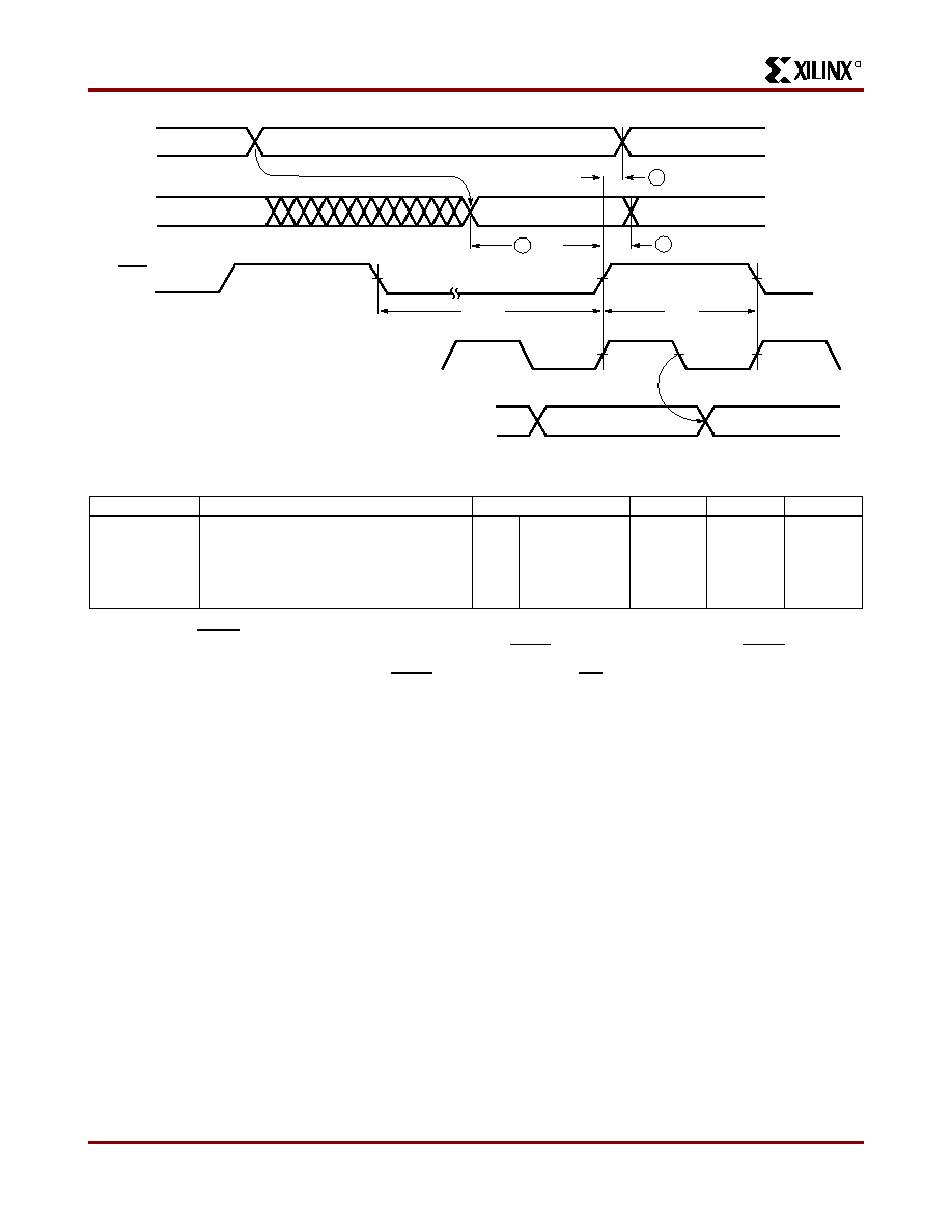
R
XC3000 Series Field Programmable Gate Arrays
7-28
November 9, 1998 (Version 3.1)
Notes:
1. At power-up, V
CC
must rise from 2.0 V to V
CC
min in less than 25 ms. If this is not possible, configuration can be delayed by
holding RESET Low until VCC has reached 4.0 V (2.5 V for the XC3000L). A very long V
CC
rise time of >100 ms, or a
non-monotonically rising V
CC
may require a >6-
�
s High level on RESET, followed by a >6-
�
s Low level on RESET and D/P
after V
CC
has reached 4.0 V (2.5 V for the XC3000L).
2. Configuration can be controlled by holding RESET Low with or until after the INIT of all daisy-chain slave-mode devices is
High.
This timing diagram shows that the EPROM requirements are extremely relaxed:
EPROM access time can be longer than 4000 ns. EPROM data output has no hold time requirements.
Figure 26: Master Parallel Mode Programming Switching Characteristics
Address for Byte n
Byte
2 T
DRC
Address for Byte n + 1
D7
D6
A0-A15
(output)
D0-D7
RCLK
(output)
CCLK
(output)
DOUT
(output)
1 T
RAC
7 CCLKs
CCLK
3 T
RCD
Byte n - 1
X5380
Description
Symbol
Min
Max
Units
RCLK
To address valid
To data setup
To data hold
RCLK High
RCLK Low
1
2
3
T
RAC
T
DRC
T
RCD
T
RCH
T
RCL
0
60
0
600
4.0
200
ns
ns
ns
ns
�
s
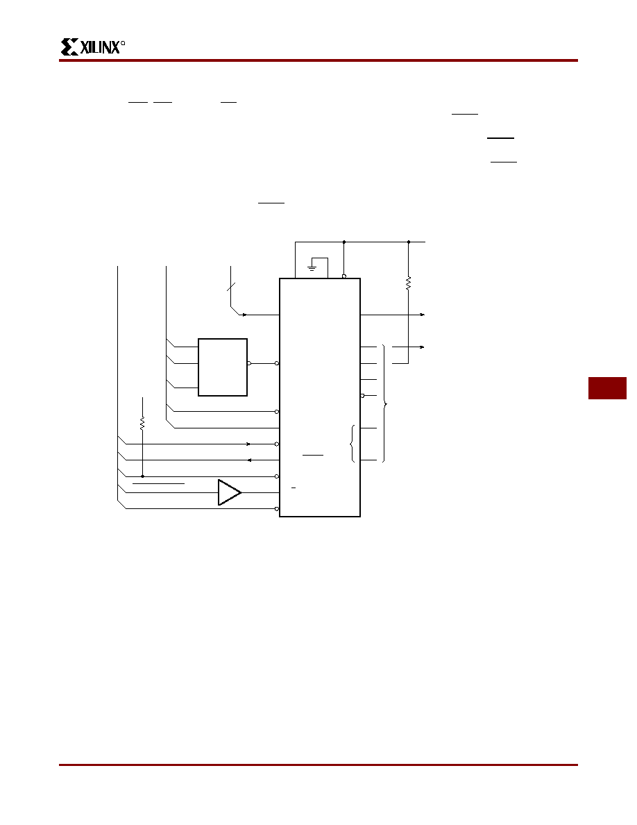
R
November 9, 1998 (Version 3.1)
7-29
XC3000 Series Field Programmable Gate Arrays
7
Peripheral Mode
Peripheral mode uses the trailing edge of the logic AND
condition of the CS0, CS1, CS2, and WS inputs to accept
byte-wide data from a microprocessor bus. In the lead
FPGA, this data is loaded into a double-buffered UART-like
parallel-to-serial converter and is serially shifted into the
internal logic. The lead FPGA presents the preamble data
(and all data that overflows the lead device) on the DOUT
pin.
The Ready/Busy output from the lead device acts as a
handshake signal to the microprocessor. RDY/BUSY goes
Low when a byte has been received, and goes High again
when the byte-wide input buffer has transferred its informa-
tion into the shift register, and the buffer is ready to receive
new data. The length of the BUSY signal depends on the
activity in the UART. If the shift register had been empty
when the new byte was received, the BUSY signal lasts for
only two CCLK periods. If the shift register was still full
when the new byte was received, the BUSY signal can be
as long as nine CCLK periods.
Note that after the last byte has been entered, only seven
of its bits are shifted out. CCLK remains High with DOUT
equal to bit 6 (the next-to-last bit) of the last byte entered.
X5991
ADDRESS
BUS
DATA
BUS
D0�7
ADDRESS
DECODE
LOGIC
CS0
...
RDY/BUSY
WS
RESET
...
OTHER
I/O PINS
D0�7
CCLK
DOUT
M2
HDC
LDC
FPGA
GENERAL-
PURPOSE
USER I/O
PINS
D/P
M0
M1 PWR
DWN
+5 V
CS2
CS1
CONTROL
SIGNALS
8
INIT
REPROGRAM
+5 V
5 k
*
IF READBACK IS
ACTIVATED, A
5-k
RESISTOR IS
REQUIRED IN SERIES
WITH M1
*
OPTIONAL
DAISY-CHAINED
FPGAs WITH DIFFERENT
CONFIGURATIONS
OC
Figure 27: Peripheral Mode Circuit Diagram
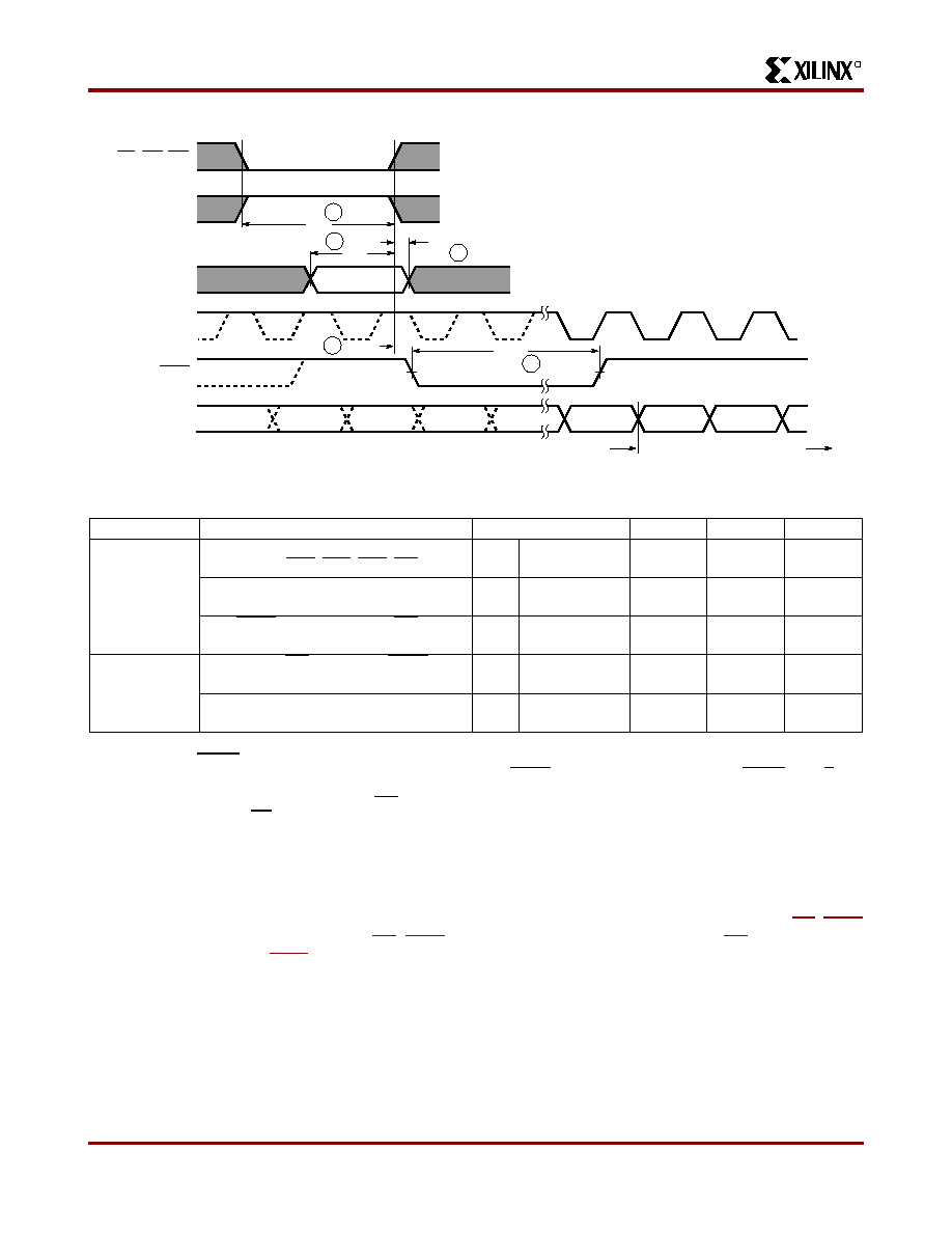
R
XC3000 Series Field Programmable Gate Arrays
7-30
November 9, 1998 (Version 3.1)
Notes:
1. At power-up, V
CC
must rise from 2.0 V to V
CC
min in less than 25 ms. If this is not possible, configuration can be delayed by
holding RESET Low until V
CC
has reached 4.0 V (2.5 V for the XC3000L). A very long V
CC
rise time of >100 ms, or a
non-monotonically rising V
CC
may require a >6-
�
s High level on RESET, followed by a >6-
�
s Low level on RESET and D/P
after V
CC
has reached 4.0 V (2.5 V for the XC3000L).
2. Configuration must be delayed until the INIT of all FPGAs is High.
3. Time from end of WS to CCLK cycle for the new byte of data depends on completion of previous byte processing and the
phase of the internal timing generator for CCLK.
4. CCLK and DOUT timing is tested in slave mode.
5. T
BUSY
indicates that the double-buffered parallel-to-serial converter is not yet ready to receive new data. The shortest T
BUSY
occurs when a byte is loaded into an empty parallel-to-serial converter. The longest TBUSY occurs when a new word is
loaded into the input register before the second-level buffer has started shifting out data.
Note:
This timing diagram shows very relaxed requirements: Data need not be held beyond the rising edge of WS. BUSY
will go active within 60 ns after the end of WS. BUSY will stay active for several microseconds. WS may be asserted
immediately after the end of BUSY.
Figure 28: Peripheral Mode Programming Switching Characteristics
6
BUSY
T
D6
DOUT
RDY/BUSY
D7
D0
D1
D2
4
WTRB
T
Valid
2
DC
T
1
CA
T
CCLK
D0-D7
CS2
WS, CS0, CS1
3
CD
T
WRITE TO FPGA
X5992
Previous Byte
New Byte
Description
Symbol
Min
Max
Units
WRITE
Effective Write time required
(Assertion of CS0, CS1, CS2, WS)
1
T
CA
100
ns
DIN Setup time required
DIN Hold time required
2
3
T
DC
T
CD
60
0
ns
ns
RDY/BUSY delay after end of WS
4
T
WTRB
60
ns
RDY
Earliest next WS after end of BUSY
5
T
RBWT
0
ns
BUSY Low time generated
6
T
BUSY
2.5
9
CCLK
periods
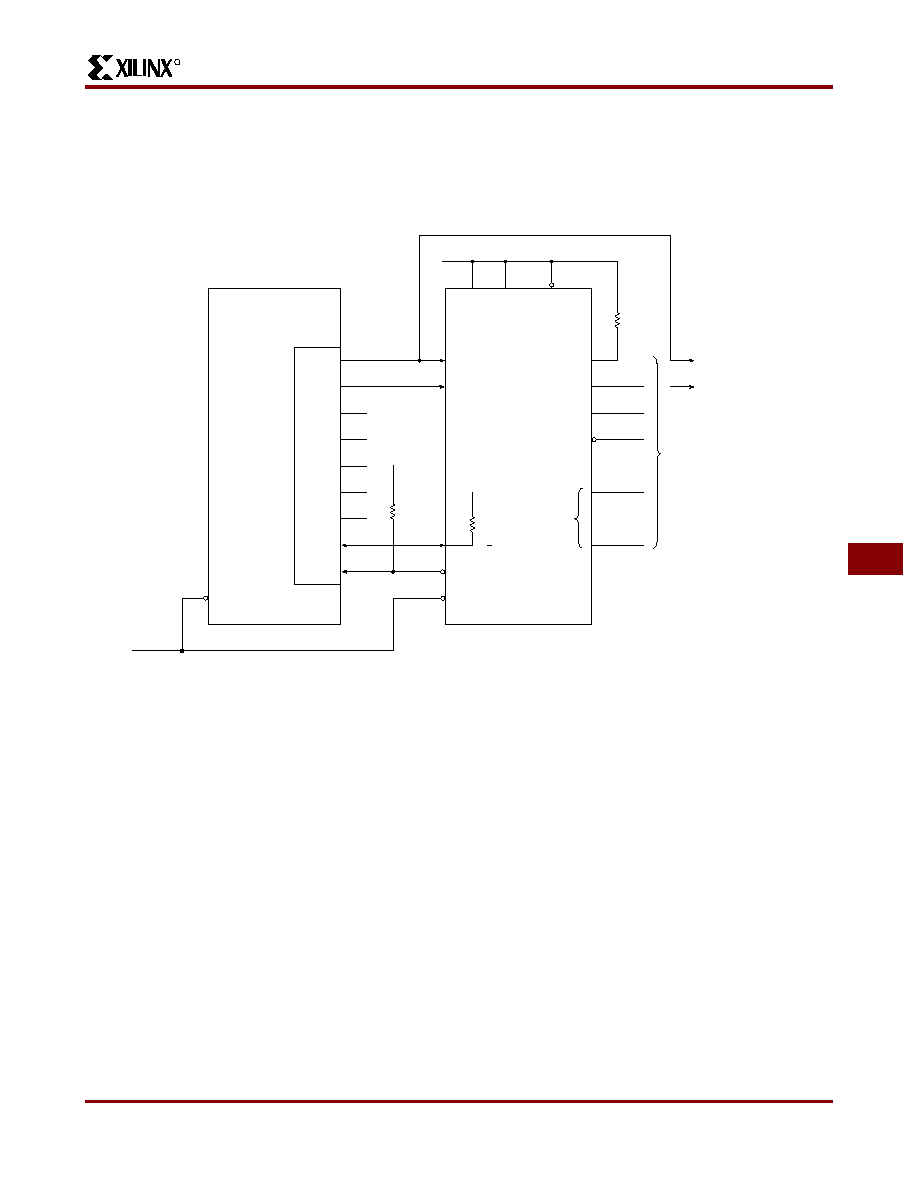
R
November 9, 1998 (Version 3.1)
7-31
XC3000 Series Field Programmable Gate Arrays
7
Slave Serial Mode
In Slave Serial mode, an external signal drives the CCLK
input(s) of the FPGA(s). The serial configuration bitstream
must be available at the DIN input of the lead FPGA a short
set-up time before each rising CCLK edge. The lead device
then presents the preamble data (and all data that over-
flows the lead device) on its DOUT pin. There is an internal
delay of 0.5 CCLK periods, which means that DOUT
changes on the falling CCLK edge, and the next device in
the daisy-chain accepts data on the subsequent rising
CCLK edge.
D/P
RESET
X5993
FPGA
General-
Purpose
User I/O
Pins
+5 V
M0
M1
PWRDWN
CCLK
DIN
STRB
D0
D1
D2
D3
D4
D5
D6
D7
RESET
I/O
Port
Micro
Computer
DOUT
HDC
LDC
M2
...
Other
I/O Pins
INIT
+5 V
5 k
If Readback is
Activated, a
5-k
Resistor is
Required in
Series with M1
*
Optional
Daisy-Chained
LCAs with
Different
Configurations
*
Figure 29: Slave Serial Mode Circuit Diagram
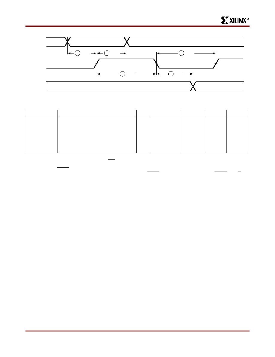
R
XC3000 Series Field Programmable Gate Arrays
7-32
November 9, 1998 (Version 3.1)
Notes: 1. The max limit of CCLK Low time is caused by dynamic circuitry inside the FPGA.
2. Configuration must be delayed until the INIT of all FPGAs is High.
3. At power-up, V
CC
must rise from 2.0 V to V
CC
min in less than 25 ms. If this is not possible, configuration can be delayed by
holding RESET Low until VCC has reached 4.0 V (2.5 V for the XC3000L). A very long V
CC
rise time of >100 ms, or a
non-monotonically rising V
CC
may require a >6-
�
s High level on RESET, followed by a >6-
�
s Low level on RESET and D/P
after V
CC
has reached 4.0 V (2.5 V for the XC3000L).
Figure 30: Slave Serial Mode Programming Switching Characteristics
4 T
CCH
Bit n
Bit n + 1
Bit n
Bit n - 1
3 T
CCO
5 T
CCL
2 T
CCD
1 T
DCC
DIN
CCLK
DOUT
(Output)
X5379
Description
Symbol
Min
Max
Units
CCLK
To DOUT
DIN setup
DIN hold
High time
Low time (Note 1)
Frequency
3
1
2
4
5
T
CCO
T
DCC
T
CCD
T
CCH
T
CCL
F
CC
60
0
0.05
0.05
100
5.0
10
ns
ns
ns
�
s
�
s
MHz
R
November 9, 1998 (Version 3.1)
7-33
XC3000 Series Field Programmable Gate Arrays
7
Program Readback Switching Characteristics
Notes:
1. During Readback, CCLK frequency may not exceed 1 MHz.
2. RETRIG (M0 positive transition) shall not be done until after one clock following active I/O pins.
3. Readback should not be initiated until configuration is complete.
4. T
CCLR
is 5
�
s min to 15
�
s max for XC3000L.
1 T
RTH
5
3
4
4
2
T
CCL
T
CCRD
T
CCL
T
RTCC
DONE/PROG
(OUTPUT)
X6116
RTRIG (M0)
CCLK(1)
VALID
READBACK OUTPUT
HI-Z
VALID
READBACK OUTPUT
M1 Input/
RDATA Output
Description
Symbol
Min
Max
Units
RTRIG
RTRIG High
1
T
RTH
250
ns
CCLK
RTRIG setup
RDATA delay
High time
Low time
2
3
4
5
T
RTCC
T
CCRD
T
CCHR
T
CCLR
200
0.5
0.5
100
5
ns
ns
�
s
�
s
R
XC3000 Series Field Programmable Gate Arrays
7-34
November 9, 1998 (Version 3.1)
General XC3000 Series Switching Characteristics
Notes:
1. At power-up, V
CC
must rise from 2.0 V to V
CC
min in less than 25 ms. If this is not possible, configuration can be delayed by
holding RESET Low until Vcc has reached 4.0 V (2.5 V for XC3000L). A very long Vcc rise time of >100 ms, or a
non-monotonically rising V
CC
may require a >1-
�
s High level on RESET, followed by a >6-
�
s Low level on RESET and D/P
after Vcc has reached 4.0 V (2.5 V for XC3000L).
2. RESET timing relative to valid mode lines (M0, M1, M2) is relevant when RESET is used to delay configuration. The
specified hold time is caused by a shift-register filter slowing down the response to RESET during configuration.
3. PWRDWN transitions must occur while V
CC
>4.0 V(2.5 V for XC3000L).
4 T
MRW
2 T
MR
3 T
RM
5 T
PGW
6 T
PGI
Clear State
Configuration State
User State
Note 3
V
CCPD
X5387
RESET
M0/M1/M2
DONE/PROG
INIT
(Output)
PWRDWN
V
CC
(Valid)
Description
Symbol
Min
Max
Units
RESET (2)
M0, M1, M2 setup time required
M0, M1, M2 hold time required
RESET Width (Low) req. for Abort
2
3
4
T
MR
T
RM
T
MRW
1
4.5
6
�
s
�
s
�
s
DONE/PROG
Width (Low) required for Re-config.
INIT response after D/P is pulled Low
5
6
T
PGW
T
PGI
6
7
�
s
�
s
PWRDWN (3)
Power Down V
CC
V
CCPD
2.3
V

R
November 9, 1998 (Version 3.1)
7-35
XC3000 Series Field Programmable Gate Arrays
7
Device Performance
The XC3000 families of FPGAs can achieve very high per-
formance. This is the result of
�
A sub-micron manufacturing process, developed and
continuously being enhanced for the production of
state-of-the-art CMOS SRAMs.
�
Careful optimization of transistor geometries, circuit
design, and lay-out, based on years of experience with
the XC3000 family.
�
A look-up table based, coarse-grained architecture that
can collapse multiple-layer combinatorial logic into a
single function generator. One CLB can implement up
to four layers of conventional logic in as little as 1.5 ns.
Actual system performance is determined by the timing of
critical paths, including the delay through the combinatorial
and sequential logic elements within CLBs and IOBs, plus
the delay in the interconnect routing. The AC-timing speci-
fications state the worst-case timing parameters for the var-
ious logic resources available in the XC3000-families
architecture.
Figure 31
shows a variety of elements
involved in determining system performance.
Logic block performance is expressed as the propagation
time from the interconnect point at the input to the block to
the output of the block in the interconnect area. Since com-
binatorial logic is implemented with a memory lookup table
within a CLB, the combinatorial delay through the CLB,
called T
ILO
, is always the same, regardless of the function
being implemented. For the combinatorial logic function
driving the data input of the storage element, the critical
timing is data set-up relative to the clock edge provided to
the flip-flop element. The delay from the clock source to the
output of the logic block is critical in the timing signals pro-
duced by storage elements. Loading of a logic-block output
is limited only by the resulting propagation delay of the
larger interconnect network. Speed performance of the
logic block is a function of supply voltage and temperature.
See
Figure 32
.
Interconnect performance depends on the routing
resources used to implement the signal path. Direct inter-
connects to the neighboring CLB provide an extremely fast
path. Local interconnects go through switch matrices
(magic boxes) and suffer an RC delay, equal to the resis-
tance of the pass transistor multiplied by the capacitance of
the driven metal line. Longlines carry the signal across the
length or breadth of the chip with only one access delay.
Generous on-chip signal buffering makes performance rel-
atively insensitive to signal fan-out; increasing fan-out from
1 to 8 changes the CLB delay by only 10%. Clocks can be
distributed with two low-skew clock distribution networks.
The tools in the Development System used to place and
route a design in an XC3000 FPGA automatically calculate
the actual maximum worst-case delays along each signal
path. This timing information can be back-annotated to the
design's netlist for use in timing simulation or examined
with, a static timing analyzer.
Actual system performance is applications dependent. The
maximum clock rate that can be used in a system is deter-
mined by the critical path delays within that system. These
delays are combinations of incremental logic and routing
delays, and vary from design to design. In a synchronous
system, the maximum clock rate depends on the number of
combinatorial logic layers between re-synchronizing
flip-flops.
Figure 33
shows the achievable clock rate as a
function of the number of CLB layers.
CLB
CLB
IOB
CLB
PAD
(K)
Logic
Logic
CKO
T
CLOCK
Clock to Output
Combinatorial
Setup
T
CKO
T
ILO
T
ICK
(K)
PAD
IOB
T
PID
T
OKPO
OP
T
X3178
Figure 31: Primary Block Speed Factors. Actual timing is a function of various block factors combined with routing.
factors. Overall performance can be evaluated with the timing calculator or by an optional simulation.

R
XC3000 Series Field Programmable Gate Arrays
7-36
November 9, 1998 (Version 3.1)
Power
Power Distribution
Power for the FPGA is distributed through a grid to achieve
high noise immunity and isolation between logic and I/O.
Inside the FPGA, a dedicated V
CC
and ground ring sur-
rounding the logic array provides power to the I/O drivers.
An independent matrix of V
CC
and groundlines supplies the
interior logic of the device. This power distribution grid pro-
vides a stable supply and ground for all internal logic, pro-
viding the external package power pins are all connected
and appropriately decoupled. Typically a 0.1-
�
F capacitor
connected near the V
CC
and ground pins will provide ade-
quate decoupling.
Output buffers capable of driving the specified 4- or 8-mA
loads under worst-case conditions may be capable of driv-
ing as much as 25 to 30 times that current in a best case.
Noise can be reduced by minimizing external load capaci-
tance and reducing simultaneous output transitions in the
same direction. It may also be beneficial to locate heavily
loaded output buffers near the ground pads. The I/O Block
output buffers have a slew-limited mode which should be
used where output rise and fall times are not speed critical.
Slew-limited outputs maintain their dc drive capability, but
generate less external reflections and internal noise.
1.00
0.80
0.60
0.40
0.20
SPECIFIED WORST-CASE VALUES
MAX CO
MMERCIAL (4.75 V)
MAX MILITARY (4.5 V)
� 55
MIN MILITARY (5.5 V)
MIN COMMERCIAL (4.75 V)
MIN COMMERCIAL (5.25 V)
TYPICAL COMMERCIAL
(+ 5.0 V, 25
�
C)
TYPICAL MILITARY
TEMPERATURE (
�
C)
� 40
� 20
0
25
40
70
80
100
125
NORMALIZED DELAY
X6094
MIN MILITARY (4.5 V)
Figure 32: Relative Delay as a Function of Temperature, Supply Voltage and Processing Variations
System Clock (MHz)
250
200
150
100
50
3 CLBs
(3-12)
4 CLBs
(4-16)
2 CLBs
(2-8)
1 CLB
(1-4)
XC3100A-3
XC3000A--6
CLB Levels:
Gate Levels:
300
Toggle
Rate
0
X7065
Figure 33: Clock Rate as a Function of Logic
Complexity (Number of Combinational Levels between
Flip-Flops)

R
November 9, 1998 (Version 3.1)
7-37
XC3000 Series Field Programmable Gate Arrays
7
Dynamic Power Consumption
Power Consumption
The Field Programmable Gate Array exhibits the low power
consumption characteristic of CMOS ICs. For any design,
the configuration option of TTL chip input threshold
requires power for the threshold reference. The power
required by the static memory cells that hold the configura-
tion data is very low and may be maintained in a
power-down mode.
Typically, most of power dissipation is produced by external
capacitive loads on the output buffers. This load and fre-
quency dependent power is 25
�
W/pF/MHz per output.
Another component of I/O power is the external dc loading
on all output pins.
Internal power dissipation is a function of the number and
size of the nodes, and the frequency at which they change.
In an FPGA, the fraction of nodes changing on a given
clock is typically low (10-20%). For example, in a long
binary counter, the total activity of all counter flip-flops is
equivalent to that of only two CLB outputs toggling at the
clock frequency. Typical global clock-buffer power is
between 2.0 mW/MHz for the XC3020A and 3.5 mW/MHz
for the XC3090A. The internal capacitive load is more a
function of interconnect than fan-out. With a typical load of
three general interconnect segments, each CLB output
requires about 0.25 mW per MHz of its output frequency.
Because the control storage of the FPGA is CMOS static
memory, its cells require a very low standby current for data
retention. In some systems, this low data retention current
characteristic can be used as a method of preserving con-
figurations in the event of a primary power loss. The FPGA
has built in powerdown logic which, when activated, will
disable normal operation of the device and retain only the
configuration data. All internal operation is suspended and
output buffers are placed in their high-impedance state with
no pull-ups. Different from the XC3000 family which can be
powered down to a current consumption of a few micro-
amps, the XC3100A draws 5 mA, even in power-down.
This makes power-down operation less meaningful. In con-
trast, I
CCPD
for the XC3000L is only 10
�
A.
To force the FPGA into the Powerdown state, the user must
pull the PWRDWN pin Low and continue to supply a reten-
tion voltage to the V
CC
pins. When normal power is
restored, V
CC
is elevated to its normal operating voltage
and PWRDWN is returned to a High. The FPGA resumes
operation with the same internal sequence that occurs at
the conclusion of configuration. Internal-I/O and logic-block
storage elements will be reset, the outputs will become
enabled and the DONE/PROG pin will be released.
When V
CC
is shut down or disconnected, some power
might unintentionally be supplied from an incoming signal
driving an I/O pin. The conventional electrostatic input pro-
tection is implemented with diodes to the supply and
ground. A positive voltage applied to an input (or output)
will cause the positive protection diode to conduct and drive
the V
CC
connection. This condition can produce invalid
power conditions and should be avoided. A large series
resistor might be used to limit the current or a bipolar buffer
may be used to isolate the input signal.
XC3042A
XC3042L
XC3142A
One CLB driving three local interconnects
0.25
0.17
0.25
mW per MHz
One global clock buffer and clock line
2.25
1.40
1.70
mW per MHz
One device output with a 50 pF load
1.25
1.25
1.25
mW per MHz
R
XC3000 Series Field Programmable Gate Arrays
7-38
November 9, 1998 (Version 3.1)
Pin Descriptions
Permanently Dedicated Pins
V
CC
Two to eight (depending on package type) connections to
the positive V supply voltage. All must be connected.
GND
Two to eight (depending on package type) connections to
ground. All must be connected.
PWRDWN
A Low on this CMOS-compatible input stops all internal
activity, but retains configuration. All flip-flops and latches
are reset, all outputs are 3-stated, and all inputs are inter-
preted as High, independent of their actual level. When
PWDWN returns High, the FPGA becomes operational
with DONE Low for two cycles of the internal 1-MHz clock.
Before and during configuration, PWRDWN must be High.
If not used, PWRDWN must be tied to V
CC
.
RESET
This is an active Low input which has three functions.
Prior to the start of configuration, a Low input will delay the
start of the configuration process. An internal circuit senses
the application of power and begins a minimal time-out
cycle. When the time-out and RESET are complete, the
levels of the M lines are sampled and configuration begins.
If RESET is asserted during a configuration, the FPGA is
re-initialized and restarts the configuration at the termina-
tion of RESET.
If RESET is asserted after configuration is complete, it pro-
vides a global asynchronous RESET of all IOB and CLB
storage elements of the FPGA.
CCLK
During configuration, Configuration Clock is an output of an
FPGA in Master mode or Peripheral mode, but an input in
Slave mode. During Readback, CCLK is a clock input for
shifting configuration data out of the FPGA.
CCLK drives dynamic circuitry inside the FPGA. The Low
time may, therefore, not exceed a few microseconds. When
used as an input, CCLK must be "parked High". An internal
pull-up resistor maintains High when the pin is not being
driven.
DONE/PROG (D/P)
DONE is an open-drain output, configurable with or without
an internal pull-up resistor of 2 to 8 k
. At the completion of
configuration, the FPGA circuitry becomes active in a syn-
chronous order; DONE is programmed to go active High
one cycle either before or after the outputs go active.
Once configuration is done, a High-to-Low transition of this
pin will cause an initialization of the FPGA and start a
reconfiguration.
M0/RTRIG
As Mode 0, this input is sampled on power-on to determine
the power-on delay (2
14
cycles if M0 is High, 2
16
cycles if M0
is Low). Before the start of configuration, this input is again
sampled together with M1, M2 to determine the configura-
tion mode to be used.
A Low-to-High input transition, after configuration is com-
plete, acts as a Read Trigger and initiates a Readback of
configuration and storage-element data clocked by CCLK.
By selecting the appropriate Readback option when gener-
ating the bitstream, this operation may be limited to a single
Readback, or be inhibited altogether.
M1/RDATA
As Mode 1, this input and M0, M2 are sampled before the
start of configuration to establish the configuration mode to
be used. If Readback is never used, M1 can be tied directly
to ground or V
CC
. If Readback is ever used, M1 must use a
5-k
resistor to ground or V
CC
, to accommodate the
RDATA output.
As an active-Low Read Data, after configuration is com-
plete, this pin is the output of the Readback data.
User I/O Pins That Can Have Special
Functions
M2
During configuration, this input has a weak pull-up resistor.
Together with M0 and M1, it is sampled before the start of
configuration to establish the configuration mode to be
used. After configuration, this pin is a user-programmable
I/O pin.
HDC
During configuration, this output is held at a High level to
indicate that configuration is not yet complete. After config-
uration, this pin is a user-programmable I/O pin.
LDC
During Configuration, this output is held at a Low level to
indicate that the configuration is not yet complete. After
configuration, this pin is a user-programmable I/O pin. LDC
is particularly useful in Master mode as a Low enable for an
EPROM, but it must then be programmed as a High after
configuration.
INIT
This is an active Low open-drain output with a weak pull-up
and is held Low during the power stabilization and internal
clearing of the configuration memory. It can be used to indi-
cate status to a configuring microprocessor or, as a wired

R
November 9, 1998 (Version 3.1)
7-39
XC3000 Series Field Programmable Gate Arrays
7
AND of several slave mode devices, a hold-off signal for a
master mode device. After configuration this pin becomes a
user-programmable I/O pin.
BCLKIN
This is a direct CMOS level input to the alternate clock
buffer (Auxiliary Buffer) in the lower right corner.
XTL1
This user I/O pin can be used to operate as the output of an
amplifier driving an external crystal and bias circuitry.
XTL2
This user I/O pin can be used as the input of an amplifier
connected to an external crystal and bias circuitry. The I/O
Block is left unconfigured. The oscillator configuration is
activated by routing a net from the oscillator buffer symbol
output and by the MakeBits program.
CS0, CS1, CS2, WS
These four inputs represent a set of signals, three active
Low and one active High, that are used to control configu-
ration-data entry in the Peripheral mode. Simultaneous
assertion of all four inputs generates a Write to the internal
data buffer. The removal of any assertion clocks in the
D0-D7 data. In Master-Parallel mode, WS and CS2 are the
A0 and A1 outputs. After configuration, these pins are
user-programmable I/O pins.
RDY/BUSY
During Peripheral Parallel mode configuration this pin indi-
cates when the chip is ready for another byte of data to be
written to it. After configuration is complete, this pin
becomes a user-programmed I/O pin.
RCLK
During Master Parallel mode configuration, each change
on the A0-15 outputs is preceded by a rising edge on
RCLK, a redundant output signal. After configuration is
complete, this pin becomes a user-programmed I/O pin.
D0-D7
This set of eight pins represents the parallel configuration
byte for the parallel Master and Peripheral modes. After
configuration is complete, they are user-programmed I/O
pins.
A0-A15
During Master Parallel mode, these 16 pins present an
address output for a configuration EPROM. After configura-
tion, they are user-programmable I/O pins.
DIN
During Slave or Master Serial configuration, this pin is used
as a serial-data input. In the Master or Peripheral configu-
ration, this is the Data 0 input. After configuration is com-
plete, this pin becomes a user-programmed I/O pin.
DOUT
During configuration this pin is used to output serial-config-
uration data to the DIN pin of a daisy-chained slave. After
configuration is complete, this pin becomes a user-pro-
grammed I/O pin.
TCLKIN
This is a direct CMOS-level input to the global clock buffer.
This pin can also be configured as a user programmable
I/O pin. However, since TCLKIN is the preferred input to the
global clock net, and the global clock net should be used as
the primary clock source, this pin is usually the clock input
to the chip.
Unrestricted User I/O Pins
I/O
An I/O pin may be programmed by the user to be an Input
or an Output pin following configuration. All unrestricted I/O
pins, plus the special pins mentioned on the following page,
have a weak pull-up resistor that becomes active as soon
as the device powers up, and stays active until the end of
configuration.
Note:
Before and during configuration, all outputs that are not used for the configuration process are 3-stated with a weak
pull-up resistor.
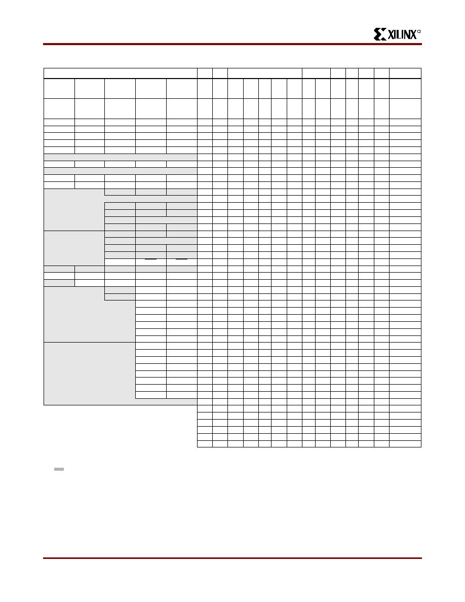
R
XC3000 Series Field Programmable Gate Arrays
7-40
November 9, 1998 (Version 3.1)
Pin Functions During Configuration
Configuration Mode <M2:M1:M0>
***
**
****
SLAVE
SERIAL
<1:1:1>
MASTER-
SERIAL
<0:0:0>
PERIPH
<1:0:1>
MASTER-
HIGH
<1:1:0>
MASTER-
LOW
<1:0:0>
44
PLCC
64
VQFP
68
PLCC
84
PLCC
84
PGA
100
PQFP
100
VQFP
TQFP
132
PGA
144
TQFP
160
PQFP
175
PGA
176
TQFP
208
PQFP
User
Function
POWR
DWN
(I)
POWER
DWN
(I)
POWER
DWN
(I)
POWER
DWN
(I)
POWER
DWN
(I)
7
17
10
12
B2
29
26
A1
1
159
B2
1
3
POWER
DWN
(1)
M1 (HIGH) (I)
M1 (LOW) (I)
M1 (LOW) (I)
M1 (HIGH) (I)
M1 (LOW) (I)
16
31
25
31
J2
52
49
B13
36
40
B14
45
48
RDATA
M0 (HIGH) (I)
M0 (LOW) (I)
M0 (HIGH) (I)
M0 (LOW) (I)
M0 (LOW) (I)
17
32
26
32
L1
54
51
A14
38
42
B15
47
50
RTRIG (I)
M2 (HIGH) (I)
M2 (LOW) (I)
M2 (HIGH) (I)
M2 (HIGH) (I)
M2 (HIGH) (I)
18
33
27
33
K2
56
53
C13
40
44
C15
49
56
I/O
HDC (HIGH)
HDC (HIGH)
HDC (HIGH)
HDC (HIGH)
HDC (HIGH)
19
34
28
34
K3
57
54
B14
41
45
E14
50
57
I/O
LDC (LOW)
LDC (LOW)
LDC (LOW)
LDC (LOW)
LDC (LOW)
20
36
30
36
L3
59
56
D14
45
49
D16
54
61
I/O
INIT*
INIT*
INIT*
INIT*
INIT*
22
40
34
42
K6
65
62
G14
53
59
H15
65
77
I/O
GND
GND
GND
GND
GND
23
41
35
43
J6
66
63
H12
55
61
J14
67
79
GND
26
47
43
53
L11
76
73
M13
69
76
P15
85
100
XTL2 OR I/O
RESET (I)
RESET (I)
RESET (I)
RESET (I)
RESET (I)
27
48
44
54
K10
78
75
P14
71
78
R15
87
102
RESET (I)
DONE
DONE
DONE
DONE
DONE
28
49
45
55
J10
80
77
N13
73
80
R14
89
107
PROGRAM (I)
DATA 7 (I)
DATA 7 (I)
DATA 7 (I)
50
46
56
K11
81
78
M12
74
81
N13
90
109
I/O
30
51
47
57
J11
82
79
P13
75
82
T14
91
110
XTL1 OR I/O
DATA 6 (I)
DATA 6 (I)
DATA 6 (I)
52
48
58
H10
83
80
N11
78
86
P12
96
115
I/O
DATA 5 (I)
DATA 5 (I)
DATA 5 (I)
53
49
60
F10
87
84
M9
84
92
T11
102
122
I/O
CS0 (I)
54
50
61
G10
88
85
N9
85
93
R10
103
123
I/O
DATA 4 (I)
DATA 4 (I)
DATA 4 (I)
55
51
62
G11
89
86
N8
88
96
R9
108
128
I/O
DATA 3 (I)
DATA 3 (I)
DATA 3 (I)
57
53
65
F11
92
89
N7
92
102
P8
112
132
I/O
CS1 (I)
58
54
66
E11
93
90
P6
93
103
R8
113
133
I/O
DATA 2 (I)
DATA 2 (I)
DATA 2 (I)
59
55
67
E10
94
91
M6
96
106
R7
118
138
I/O
DATA 1 (I)
DATA 1 (I)
DATA 1 (I)
60
56
70
D10
98
95
M5
102
114
R5
124
145
I/O
RDY/BUSY
RCLK
RCLK
61
57
71
C11
99
96
N4
103
115
P5
125
146
I/O
DIN (I)
DIN (I)
DATA 0 (I)
DATA 0 (I)
DATA 0 (I)
38
62
58
72
B11
100
97
N2
106
119
R3
130
151
I/O
DOUT
DOUT
DOUT
DOUT
DOUT
39
63
59
73
C10
1
98
M3
107
120
N4
131
152
I/O
CCLK (I)
CCLK (O)
CCLK (O)
CCLK (O)
CCLK (O)
40
64
60
74
A11
2
99
P1
108
121
R2
132
153
CCLK (I)
WS (I)
A0
A0
1
61
75
B10
5
2
M2
111
124
P2
135
161
I/O
CS2 (I)
A1
A1
2
62
76
B9
6
3
N1
112
125
M3
136
162
I/O
A2
A2
3
63
77
A10
8
5
L2
115
128
P1
140
165
I/O
A3
A3
4
64
78
A9
9
6
L1
116
129
N1
141
166
I/O
A15
A15
65
81
B6
12
9
K1
119
132
M1
146
172
5
A4
A4
5
66
82
B7
13
10
J2
120
133
L2
147
173
I/O
A14
A14
6
67
83
A7
14
11
H1
123
136
K2
150
178
I/O
A5
A5
7
68
84
C7
15
12
H2
124
137
K1
151
179
I/O
A13
A13
9
2
2
A6
17
14
G2
128
141
H2
156
184
I/O
A6
A6
10
3
3
A5
18
15
G1
129
142
H1
157
185
I/O
A12
A12
11
4
4
B5
19
16
F2
133
147
F2
164
192
I/O
A7
A7
12
5
5
C5
20
17
E1
134
148
E1
165
193
I/O
A11
A11
13
6
8
A3
23
20
D1
137
151
D1
169
199
I/O
A8
A8
14
7
9
A2
24
21
D2
138
152
C1
170
200
I/O
A10
A10
15
8
10
B3
25
22
B1
141
155
E3
173
203
I/O
A9
A9
16
9
11
A1
26
26
C2
142
156
C2
174
204
I/O
All Others
X
X
X
X
XC3x20A etc.
X
X
X
X
X
X
X
XC3x30A etc.
X
X
X
X
X
X
XC3x42A etc.
X**
X
X
XC3x64A etc.
X**
X
X
X
X
X
XC3x90A etc.
Notes:
X**
X
X
X
XC3195A
*
(I)
**
***
****
Note
:
Generic I/O pins are not shown.
For a detailed description of the configuration modes, see
page 25
through
page 34
.
For pinout details, see
page 65
through
page 76
.
Represents a weak pull-up before and during configuration.
INIT is an open drain output during configuration.
Represents an input.
Pin assignment for the XC3064A/XC3090A and XC3195A differ from those shown.
Peripheral mode and master parallel mode are not supported in the PC44 package.
Pin assignments for the XC3195A PQ208 differ from those shown.
Pin assignments of PGA Footprint PLCC sockets and PGA packages are not identical.
The information on this page is provided as a convenient summary. For detailed pin descriptions, see the preceding two pages.
Before and during configuration, all outputs that are not used for the configuration process are 3-stated with a weak pull-up resistor.
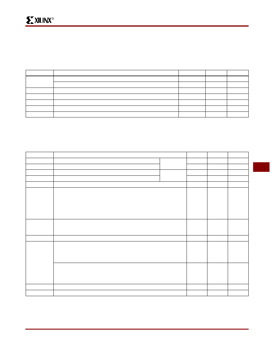
R
November 9, 1998 (Version 3.1)
7-41
XC3000 Series Field Programmable Gate Arrays
7
XC3000A Switching Characteristics
Xilinx maintains test specifications for each product as controlled documents. To insure the use of the most recently released
device performance parameters, please request a copy of the current test-specification revision.
XC3000A Operating Conditions
Note:
At junction temperatures above those listed as Operating Conditions, all delay parameters increase by 0.3% per
�
C.
XC3000A DC Characteristics Over Operating Conditions
Notes:
1. With no output current loads, no active input or Longline pull-up resistors, all package pins at V
CC
or GND, and the FPGA
device configured with a tie option.
2. Total continuous output sink current may not exceed 100 mA per ground pin. Total continuous output source may not exceed
100 mA per V
CC
pin. The number of ground pins varies from the XC3020A to the XC3090A.
3. Not tested. Allow an undriven pin to float High. For any other purposes use an external pull-up.
Symbol
Description
Min
Max
Units
V
CC
Supply voltage relative to GND Commercial 0
�
C to +85
�
C junction
4.75
5.25
V
Supply voltage relative to GND Industrial -40
�
C to +100
�
C junction
4.5
5.5
V
V
IHT
High-level input voltage -- TTL configuration
2.0
V
CC
V
V
ILT
Low-level input voltage -- TTL configuration
0
0.8
V
V
IHC
High-level input voltage -- CMOS configuration
70%
100%
V
CC
V
ILC
Low-level input voltage -- CMOS configuration
0
20%
V
CC
T
IN
Input signal transition time
250
ns
Symbol
Description
Min
Max
Units
V
OH
High-level output voltage (@ I
OH
= �4.0 mA, V
CC
min)
Commercial
3.86
V
V
OL
Low-level output voltage (@ I
OL
= 4.0 mA, V
CC
min)
0.40
V
V
OH
High-level output voltage (@ I
OH
= �4.0 mA, V
CC
min)
Industrial
3.76
V
V
OL
Low-level output voltage (@ I
OL
= 4.0 mA, V
CC
min)
0.40
V
V
CCPD
Power-down supply voltage (PWRDWN must be Low)
2.30
V
I
CCPD
Power-down supply current
(V
CC(MAX)
@ T
MAX
)
3020A
3030A
3042A
3064A
3090A
100
160
240
340
500
�
A
�
A
�
A
�
A
�
A
I
CCO
Quiescent FPGA supply current in addition to I
CCPD
Chip thresholds programmed as CMOS levels
Chip thresholds programmed as TTL levels
500
10
�
A
�
A
I
IL
Input Leakage Current
�10
+10
�
A
C
IN
Input capacitance, all packages except PGA175
(sample tested)
All Pins except XTL1 and XTL2
XTL1 and XTL2
10
15
pF
pF
Input capacitance, PGA 175
(sample tested)
All Pins except XTL1 and XTL2
XTL1 and XTL2
16
20
pF
pF
I
RIN
Pad pull-up (when selected) @ V
IN
= 0 V
3
0.02
0.17
mA
I
RLL
Horizontal Longline pull-up (when selected) @ logic Low
3.4
mA
R
XC3000 Series Field Programmable Gate Arrays
7-42
November 9, 1998 (Version 3.1)
XC3000A Absolute Maximum Ratings
Note:
Stresses beyond those listed under Absolute Maximum Ratings may cause permanent damage to the device. These are
stress ratings only, and functional operation of the device at these or any other conditions beyond those listed under
Recommended Operating Conditions is not implied. Exposure to Absolute Maximum Ratings conditions for extended
periods of time may affect device reliability.
XC3000A Global Buffer Switching Characteristics Guidelines
Note:
1. Timing is based on the XC3042A, for other devices see timing calculator.
Symbol
Description
Units
V
CC
Supply voltage relative to GND
�0.5 to +7.0
V
V
IN
Input voltage with respect to GND
�0.5 to V
CC
+0.5
V
V
TS
Voltage applied to 3-state output
�0.5 to V
CC
+0.5
V
T
STG
Storage temperature (ambient)
�65 to +150
�
C
T
SOL
Maximum soldering temperature (10 s @ 1/16 in.)
+260
�
C
T
J
Junction temperature plastic
+125
�
C
Junction temperature ceramic
+150
�
C
Speed Grade
-7
-6
Description
Symbol
Max
Max
Units
Global and Alternate Clock Distribution
1
Either: Normal IOB input pad through clock buffer
to any CLB or IOB clock input
Or: Fast (CMOS only) input pad through clock
buffer to any CLB or IOB clock input
T
PID
T
PIDC
7.5
6.0
7.0
5.7
ns
ns
TBUF driving a Horizontal Longline (L.L.)
1
I to L.L. while T is Low (buffer active)
T
to L.L. active and valid with single pull-up resistor
T
to L.L. active and valid with pair of pull-up resistors
T
to L.L. High with single pull-up resistor
T
to L.L. High with pair of pull-up resistors
T
IO
T
ON
T
ON
T
PUS
T
PUF
4.5
9.0
11.0
16.0
10.0
4.0
8.0
10.0
14.0
8.0
ns
ns
ns
ns
ns
BIDI
Bidirectional buffer delay
T
BIDI
1.7
1.5
ns
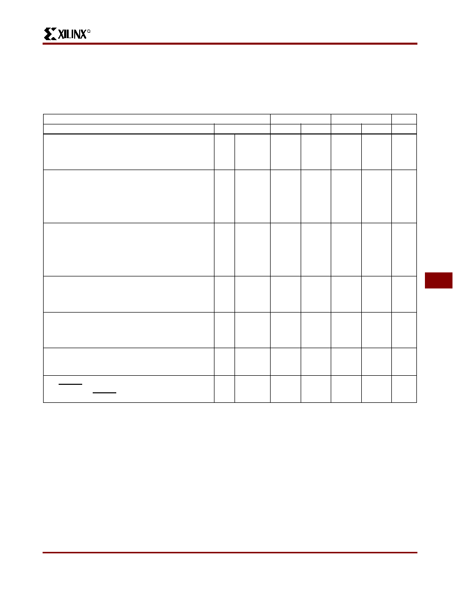
R
November 9, 1998 (Version 3.1)
7-43
XC3000 Series Field Programmable Gate Arrays
7
XC3000A CLB Switching Characteristics Guidelines
Testing of the switching parameters is modeled after testing methods specified by MIL-M-38510/605. All devices are 100%
functionally tested. Since many internal timing parameters cannot be measured directly, they are derived from benchmark
timing patterns. The following guidelines reflect worst-case values over the recommended operating conditions. For more
detailed, more precise, and more up-to-date timing information, use the values provided by the timing calculator and used
in the simulator.
Notes:
1. Timing is based on the XC3042A, for other devices see timing calculator.
2. The CLB K to Q output delay (T
CKO
, #8) of any CLB, plus the shortest possible interconnect delay, is always longer than the
Data In hold time requirement (T
CKDI
, #5) of any CLB on the same die.
Speed Grade
-7
-6
Description
Symbol
Min
Max
Min
Max
Units
Combinatorial Delay
Logic Variables
A, B, C, D, E, to outputs X or Y
FG Mode
F and FGM Mode
1
T
ILO
5.1
5.6
4.1
4.6
ns
ns
Sequential delay
Clock k to outputs X or Y
Clock k to outputs X or Y when Q is returned
through function generators F or G to drive X or Y
FG Mode
F and FGM Mode
8
T
CKO
T
QLO
4.5
9.5
10.0
4.0
8.0
8.5
ns
ns
ns
Set-up time before clock K
Logic Variables
A, B, C, D, E
FG Mode
F and FGM Mode
Data In
DI
Enable Clock
EC
2
4
6
T
ICK
T
DICK
T
ECCK
4.5
5.0
4.0
4.5
3.5
4.0
3.0
4.0
ns
ns
ns
ns
Hold Time after clock K
Logic Variables
A, B, C, D, E
Data In
DI
2
Enable Clock
EC
3
5
7
T
CKI
T
CKDI
T
CKEC
0
1.0
2.0
0
1.0
2.0
ns
ns
ns
Clock
Clock High time
Clock Low time
Max. flip-flop toggle rate
11
12
T
CH
T
CL
F
CLK
4.0
4.0
113.0
3.5
3.5
135.0
ns
ns
MHz
Reset Direct (RD)
RD width
delay from RD to outputs X or Y
13
9
T
RPW
T
RIO
6.0
6.0
5.0
5.0
ns
ns
Global Reset (RESET Pad)
1
RESET width (Low)
delay from RESET pad to outputs X or Y
T
MRW
T
MRQ
16.0
19.0
14.0
17.0
ns
ns
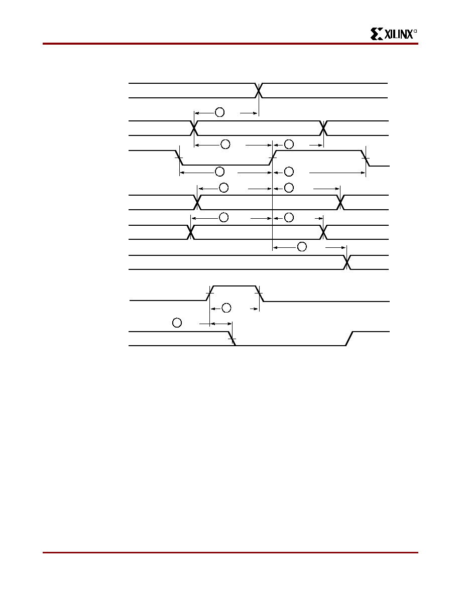
R
XC3000 Series Field Programmable Gate Arrays
7-44
November 9, 1998 (Version 3.1)
XC3000A CLB Switching Characteristics Guidelines (continued)
1
T
ILO
CLB Output (X, Y)
(Combinatorial)
CLB Input (A,B,C,D,E)
CLB Clock
CLB Input
(Direct In)
CLB Input
(Enable Clock)
CLB Output
(Flip-Flop)
CLB Input
(Reset Direct)
CLB Output
(Flip-Flop)
8
T
CKO
X5424
13 T
T
RPW
9
T
RIO
4
T
DICK
6
T
ECCK
12 T
CL
2
T
ICK
3
T
CKI
11 T
CH
5
T
CKDI
7
T
CKEC
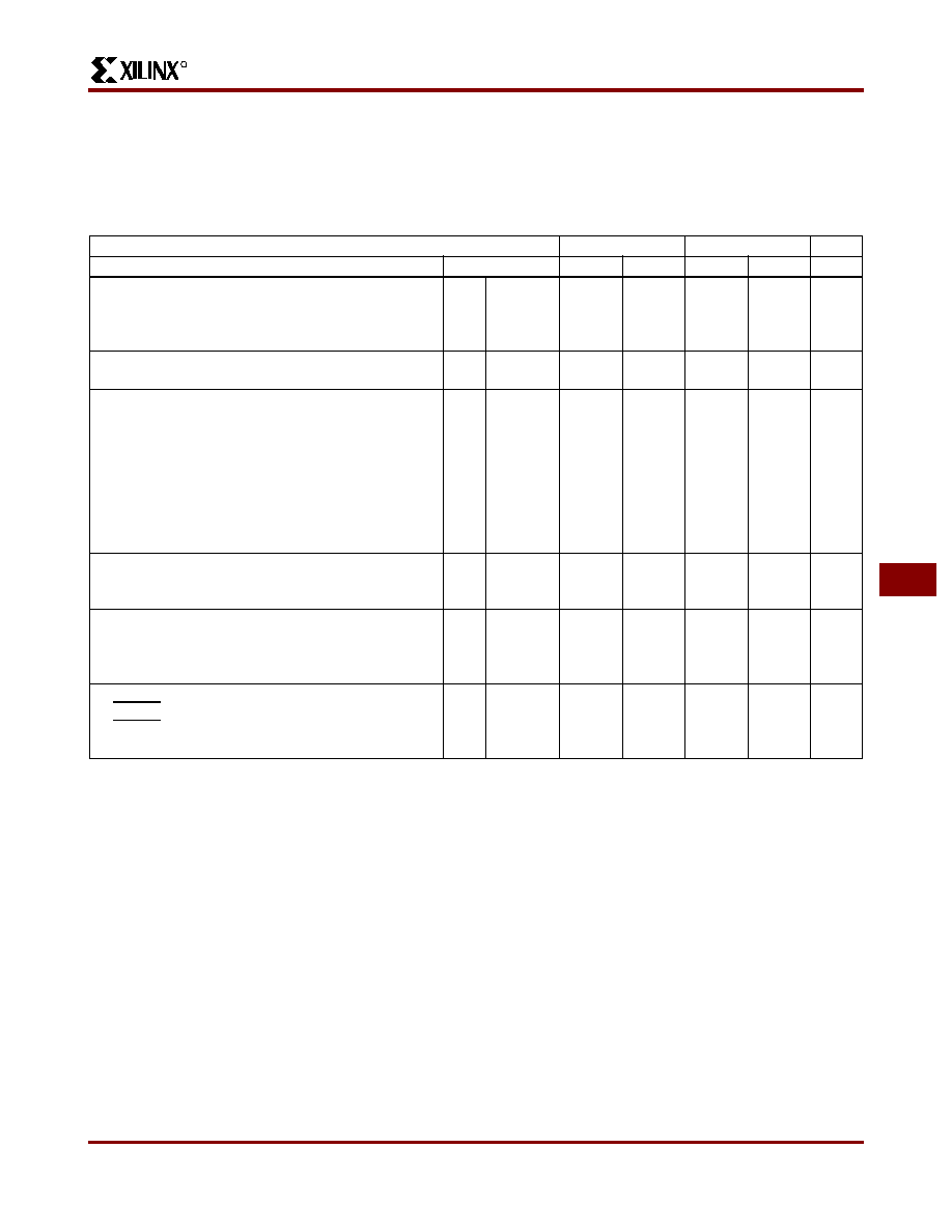
R
November 9, 1998 (Version 3.1)
7-45
XC3000 Series Field Programmable Gate Arrays
7
XC3000A IOB Switching Characteristics Guidelines
Testing of the switching parameters is modeled after testing methods specified by MIL-M-38510/605. All devices are 100%
functionally tested. Since many internal timing parameters cannot be measured directly, they are derived from benchmark
timing patterns. The following guidelines reflect worst-case values over the recommended operating conditions. For more
detailed, more precise, and more up-to-date timing information, use the values provided by the timing calculator and used
in the simulator.
Notes:
1. Timing is measured at pin threshold, with 50 pF external capacitive loads (incl. test fixture). Typical slew rate limited output
rise/fall times are approximately four times longer.
2. Voltage levels of unused (bonded and unbonded) pads must be valid logic levels. Each can be configured with the internal
pull-up resistor or alternatively configured as a driven output or driven from an external source.
3. Input pad set-up time is specified with respect to the internal clock (ik). In order to calculate system set-up time, subtract
clock delay (pad to ik) from the input pad set-up time value. Input pad holdtime with respect to the internal clock (ik) is
negative. This means that pad level changes immediately before the internal clock edge (ik) will not be recognized.
4. T
PID
, T
PTG
, and T
PICK
are 3 ns higher for XTL2 when the pin is configured as a user input.
Speed Grade
-7
-6
Description
Symbol
Min
Max
Min
Max
Units
Propagation Delays (Input)
Pad to Direct In (I)
Pad to Registered In (Q) with latch transparent
Clock (IK) to Registered In (Q)
3
4
T
PID
T
PTG
T
IKRI
4.0
15.0
3.0
3.0
14.0
2.5
ns
ns
ns
Set-up Time (Input)
Pad to Clock (IK) set-up time
1
T
PICK
14.0
12.0
ns
Propagation Delays (Output)
Clock (OK) to Pad
(fast)
same
(slew rate limited)
Output (O) to Pad
(fast)
same
(slew-rate limited)
3-state to Pad begin hi-Z
(fast)
same
(slew-rate limited)
3-state to Pad active and valid
(fast)
same
(slew -rate limited)
7
7
10
10
9
9
8
8
T
OKPO
T
OKPO
T
OPF
T
OPS
T
TSHZ
T
TSHZ
T
TSON
T
TSON
8.0
18.0
6.0
16.0
10.0
20.0
11.0
21.0
7.0
15.0
5.0
13.0
9.0
12.0
10.0
18.0
ns
ns
ns
ns
ns
ns
ns
ns
Set-up and Hold Times (Output)
Output (O) to clock (OK) set-up time
Output (O) to clock (OK) hold time
5
6
T
OOK
T
OKO
8.0
0
7.0
0
ns
ns
Clock
Clock High time
Clock Low time
Max. flip-flop toggle rate
11
12
T
IOH
T
IOL
F
CLK
4.0
4.0
113.0
3.5
3.5
135.0
ns
ns
MHz
Global Reset Delays (based on XC3042A)
RESET Pad to Registered In
(Q)
RESET Pad to output pad
(fast)
(slew-rate limited)
13
15
15
T
RRI
T
RPO
T
RPO
24.0
33.0
43.0
23.0
29.0
37.0
ns
ns
ns

R
XC3000 Series Field Programmable Gate Arrays
7-46
November 9, 1998 (Version 3.1)
XC3000A IOB Switching Characteristics Guidelines (continued)
3
T
PID
I/O Block (I)
I/O Pad Input
I/O Clock (IK/OK)
I/O Block (RI)
RESET
I/O Block (O)
I/O Pad TS
I/O Pad Output
I/O Pad Output
(Direct)
I/O Pad Output
(Registered)
X5425
5
T
OOK
12 T
IOL
1
T
PICK
11 T
IOH
4
T
IKRI
15 T
RPO
13 T
RRI
6
T
OKO
9
T
TSHZ
10 T
OP
7
T
OKPO
8
T
TSON
FLIP
FLOP
Q
D
R
SLEW
RATE
PASSIVE
PULL UP
OUTPUT
SELECT
3-STATE
INVERT
OUT
INVERT
FLIP
FLOP
or
LATCH
D
Q
R
REGISTERED IN
DIRECT IN
OUT
3- STATE
(OUTPUT ENABLE)
TTL or
CMOS
INPUT
THRESHOLD
OUTPUT
BUFFER
(GLOBAL RESET)
CK1
X3029
I/O PAD
Vcc
PROGRAM-CONTROLLED MEMORY CELLS
PROGRAMMABLE INTERCONNECTION POINT or PIP
=
IK
OK
Q
I
O
T
PROGRAM
CONTROLLED
MULTIPLEXER
CK2
R
November 9, 1998 (Version 3.1)
7-47
XC3000 Series Field Programmable Gate Arrays
7
XC3000L Switching Characteristics
Xilinx maintains test specifications for each product as controlled documents. To insure the use of the most recently released
device performance parameters, please request a copy of the current test-specification revision.
XC3000L Operating Conditions
Notes:
1. At junction temperatures above those listed as Operating Conditions, all delay parameters increase by 0.3% per
�
C.
2. Although the present (1996) devices operate over the full supply voltage range from 3.0 to 5.25 V, Xilinx reserves the right to
restrict operation to the 3.0 to 3.6 V range later, when smaller device geometries might preclude operation at 5V. Operating
conditions are guaranteed in the 3.0 � 3.6 V V
CC
range.
XC3000L DC Characteristics Over Operating Conditions
Notes:
1. With no output current loads, no active input or Longline pull-up resistors, all package pins at V
CC
or GND, and the FPGA
device configured with a tie option. I
CCO
is in addition to I
CCPD
.
2. Total continuous output sink current may not exceed 100 mA per ground pin. Total continuous output source may not exceed
100 mA per V
CC
pin. The number of ground pins varies from the XC3020L to the XC3090L.
3. Not tested. Allows an undriven pin to float High. For any other purpose, use an external pull-up.
Symbol
Description
Min
Max
Units
V
CC
Supply voltage relative to GND Commercial 0
�
C to +85
�
C junction
3.0
3.6
V
V
IH
High-level input voltage -- TTL configuration
2.0
V
CC
+0.3
V
V
IL
Low-level input voltage -- TTL configuration
-0.3
0.8
V
T
IN
Input signal transition time
250
ns
Symbol
Description
Min
Max
Units
V
OH
High-level output voltage (@ I
OH
= �4.0 mA, V
CC
min)
2.40
V
V
OL
Low-level output voltage (@ I
OL
= 4.0 mA, V
CC
min)
0.40
V
V
OH
High-level output voltage (@ I
OH
= �4.0 mA, V
CC
min)
V
CC
-0.2
V
V
OL
Low-level output voltage (@ I
OL
= 4.0 mA, V
CC
min)
0.2
V
V
CCPD
Power-down supply voltage (PWRDWN must be Low)
2.30
V
I
CCPD
Power-down supply current (V
CC(MAX)
@ T
MAX
)
10
�
A
I
CCO
Quiescent FPGA supply current in addition to I
CCPD
1
Chip thresholds programmed as CMOS levels
20
�
A
I
IL
Input Leakage Current
�10
+10
�
A
C
IN
Input capacitance, all packages except PGA175
(sample tested)
All Pins except XTL1 and XTL2
XTL1 and XTL2
10
15
pF
pF
Input capacitance, PGA 175
(sample tested)
All Pins except XTL1 and XTL2
XTL1 and XTL2
15
20
pF
pF
I
RIN
Pad pull-up (when selected) @ V
IN
= 0 V
3
0.01
0.17
mA
I
RLL
Horizontal Longline pull-up (when selected) @ logic Low
2.50
mA

R
XC3000 Series Field Programmable Gate Arrays
7-48
November 9, 1998 (Version 3.1)
XC3000L Absolute Maximum Ratings
Note:
Stresses beyond those listed under Absolute Maximum Ratings may cause permanent damage to the device. These are
stress ratings only, and functional operation of the device at these or any other conditions beyond those listed under
Recommended Operating Conditions is not implied. Exposure to Absolute Maximum Ratings conditions for extended
periods of time may affect device reliability.
XC3000L Global Buffer Switching Characteristics Guidelines
Notes: 1. Timing is based on the XC3042A, for other devices see timing calculator.
2. The use of two pull-up resistors per Longline, available on other XC3000 devices, is not a valid option for XC3000L devices.
Symbol
Description
Units
V
CC
Supply voltage relative to GND
�0.5 to +7.0
V
V
IN
Input voltage with respect to GND
�0.5 to V
CC
+0.5
V
V
TS
Voltage applied to 3-state output
�0.5 to V
CC
+0.5
V
T
STG
Storage temperature (ambient)
�65 to +150
�
C
T
SOL
Maximum soldering temperature (10 s @ 1/16 in.)
+260
�
C
T
J
Junction temperature plastic
+125
�
C
Junction temperature ceramic
+150
�
C
Speed Grade
-8
Description
Symbol
Max
Units
Global and Alternate Clock Distribution
1
Either: Normal IOB input pad through clock buffer
to any CLB or IOB clock input
Or: Fast (CMOS only) input pad through clock
buffer to any CLB or IOB clock input
T
PID
T
PIDC
9.0
7.0
ns
ns
TBUF driving a Horizontal Longline (L.L.)
1
I to L.L. while T is Low (buffer active)
T
to L.L. active and valid with single pull-up resistor
T
to L.L. High with single pull-up resistor
T
IO
T
ON
T
PUS
5.0
12.0
24.0
ns
ns
ns
BIDI
Bidirectional buffer delay
T
BIDI
2.0
ns

R
November 9, 1998 (Version 3.1)
7-49
XC3000 Series Field Programmable Gate Arrays
7
XC3000L CLB Switching Characteristics Guidelines
Testing of the switching parameters is modeled after testing methods specified by MIL-M-38510/605. All devices are 100%
functionally tested. Since many internal timing parameters cannot be measured directly, they are derived from benchmark
timing patterns. The following guidelines reflect worst-case values over the recommended operating conditions. For more
detailed, more precise, and more up-to-date timing information, use the values provided by the timing calculator and used
in the simulator.
Notes:
1. Timing is based on the XC3042L, for other devices see timing calculator.
2. The CLB K to Q output delay (T
CKO
, #8) of any CLB, plus the shortest possible interconnect delay, is always longer than the
Data In hold time requirement (T
CKDI
, #5) of any CLB on the same die.
Speed Grade
-8
Description
Symbol
Min
Max
Units
Combinatorial Delay
Logic Variables
A, B, C, D, E, to outputs X or Y
FG Mode
F and FGM Mode
1
T
ILO
6.7
7.5
ns
ns
Sequential delay
Clock k to outputs X or Y
Clock k to outputs X or Y when Q is returned
through function generators F or G to drive X or Y
FG Mode
F and FGM Mode
8
T
CKO
T
QLO
7.5
14.0
14.8
ns
ns
ns
Set-up time before clock K
Logic Variables
A, B, C, D, E
FG Mode
F and FGM Mode
Data In
DI
Enable Clock
EC
2
4
6
T
ICK
T
DICK
T
ECCK
5.0
5.8
5.0
6.0
ns
ns
ns
ns
Hold Time after clock K
Logic Variables
A, B, C, D, E
Data In
DI
2
Enable Clock
EC
3
5
7
T
CKI
T
CKDI
T
CKEC
0
2.0
2.0
ns
ns
ns
Clock
Clock High time
Clock Low time
Max. flip-flop toggle rate
11
12
T
CH
T
CL
F
CLK
5.0
5.0
80.0
ns
ns
MHz
Reset Direct (RD)
RD width
delay from RD to outputs X or Y
13
9
T
RPW
T
RIO
7.0
7.0
ns
ns
Global Reset (RESET Pad)
1
RESET width (Low)
delay from RESET pad to outputs X or Y
T
MRW
T
MRQ
16.0
23.0
ns
ns

R
XC3000 Series Field Programmable Gate Arrays
7-50
November 9, 1998 (Version 3.1)
XC3000L CLB Switching Characteristics Guidelines (continued)
1
T
ILO
CLB Output (X, Y)
(Combinatorial)
CLB Input (A,B,C,D,E)
CLB Clock
CLB Input
(Direct In)
CLB Input
(Enable Clock)
CLB Output
(Flip-Flop)
CLB Input
(Reset Direct)
CLB Output
(Flip-Flop)
8
T
CKO
X5424
13 T
T
RPW
9
T
RIO
4
T
DICK
6
T
ECCK
12 T
CL
2
T
ICK
3
T
CKI
11 T
CH
5
T
CKDI
7
T
CKEC

R
November 9, 1998 (Version 3.1)
7-51
XC3000 Series Field Programmable Gate Arrays
7
XC3000L IOB Switching Characteristics Guidelines
Testing of the switching parameters is modeled after testing methods specified by MIL-M-38510/605. All devices are 100%
functionally tested. Since many internal timing parameters cannot be measured directly, they are derived from benchmark
timing patterns. The following guidelines reflect worst-case values over the recommended operating conditions. For more
detailed, more precise, and more up-to-date timing information, use the values provided by the timing calculator and used
in the simulator.
Notes:
1. Timing is measured at pin threshold, with 50 pF external capacitive loads (incl. test fixture). Typical slew rate limited output
rise/fall times are approximately four times longer.
2. Voltage levels of unused (bonded and unbonded) pads must be valid logic levels. Each can be configured with the internal
pull-up resistor or alternatively configured as a driven output or driven from an external source.
3. Input pad set-up time is specified with respect to the internal clock (ik). In order to calculate system set-up time, subtract
clock delay (pad to ik) from the input pad set-up time value. Input pad holdtime with respect to the internal clock (ik) is
negative. This means that pad level changes immediately before the internal clock edge (ik) will not be recognized.
4. T
PID
, T
PTG
, and T
PICK
are 3 ns higher for XTL2 when the pin is configured as a user input.
Speed Grade
-8
Description
Symbol
Min
Max
Units
Propagation Delays (Input)
Pad to Direct In (I)
Pad to Registered In (Q) with latch transparent
Clock (IK) to Registered In (Q)
3
4
T
PID
T
PTG
T
IKRI
5.0
24.0
6.0
ns
ns
ns
Set-up Time (Input)
Pad to Clock (IK) set-up time
1
T
PICK
22.0
ns
Propagation Delays (Output)
Clock (OK) to Pad
(fast)
same
(slew rate limited)
Output (O) to Pad
(fast)
same
(slew-rate limited)
3-state to Pad begin hi-Z
(fast)
same
(slew-rate limited)
3-state to Pad active and valid
(fast)
same
(slew -rate limited)
7
7
10
10
9
9
8
8
T
OKPO
T
OKPO
T
OPF
T
OPS
T
TSHZ
T
TSHZ
T
TSON
T
TSON
12.0
28.0
9.0
25.0
12.0
28.0
16.0
32.0
ns
ns
ns
ns
ns
ns
ns
ns
Set-up and Hold Times (Output)
Output (O) to clock (OK) set-up time
Output (O) to clock (OK) hold time
5
6
T
OOK
T
OKO
12.0
0
ns
ns
Clock
Clock High time
Clock Low time
Max. flip-flop toggle rate
11
12
T
IOH
T
IOL
F
CLK
5.0
5.0
80.0
ns
ns
MHz
Global Reset Delays (based on XC3042L)
RESET Pad to Registered In
(Q)
RESET Pad to output pad
(fast)
(slew-rate limited)
13
15
15
T
RRI
T
RPO
T
RPO
25.0
35.0
51.0
ns
ns
ns

R
XC3000 Series Field Programmable Gate Arrays
7-52
November 9, 1998 (Version 3.1)
XC3000L IOB Switching Characteristics Guidelines (continued)
3
T
PID
I/O Block (I)
I/O Pad Input
I/O Clock (IK/OK)
I/O Block (RI)
RESET
I/O Block (O)
I/O Pad TS
I/O Pad Output
I/O Pad Output
(Direct)
I/O Pad Output
(Registered)
X5425
5
T
OOK
12 T
IOL
1
T
PICK
11 T
IOH
4
T
IKRI
15 T
RPO
13 T
RRI
6
T
OKO
9
T
TSHZ
10 T
OP
7
T
OKPO
8
T
TSON
FLIP
FLOP
Q
D
R
SLEW
RATE
PASSIVE
PULL UP
OUTPUT
SELECT
3-STATE
INVERT
OUT
INVERT
FLIP
FLOP
or
LATCH
D
Q
R
REGISTERED IN
DIRECT IN
OUT
3- STATE
(OUTPUT ENABLE)
TTL or
CMOS
INPUT
THRESHOLD
OUTPUT
BUFFER
(GLOBAL RESET)
CK1
X3029
I/O PAD
Vcc
PROGRAM-CONTROLLED MEMORY CELLS
PROGRAMMABLE INTERCONNECTION POINT or PIP
=
IK
OK
Q
I
O
T
PROGRAM
CONTROLLED
MULTIPLEXER
CK2
R
November 9, 1998 (Version 3.1)
7-53
XC3000 Series Field Programmable Gate Arrays
7
XC3100A Switching Characteristics
Xilinx maintains test specifications for each product as controlled documents. To insure the use of the most recently released
device performance parameters, please request a copy of the current test-specification revision.
XC3100A Operating Conditions
Note:
At junction temperatures above those listed as Operating Conditions, all delay parameters increase by 0.3% per
�
C.
XC3100A DC Characteristics Over Operating Conditions
Notes:
1. With no output current loads, no active input or Longline pull-up resistors, all package pins at V
CC
or GND, and the LCA
device configured with a tie option.
2. Total continuous output sink current may not exceed 100 mA per ground pin. The number of ground pins varies from two for
the XC3120A in the PC84 package, to eight for the XC3195A in the PQ208 package.
3. Not tested. Allows an undriven pin to float High. For any other purpose, use an external pull-up.
Symbol
Description
Min
Max
Units
V
CC
Supply voltage relative to GND Commercial 0
�
C to +85
�
C junction
4.25
5.25
V
Supply voltage relative to GND Industrial -40
�
C to +100
�
C junction
4.5
5.5
V
V
IHT
High-level input voltage -- TTL configuration
2.0
V
CC
V
V
ILT
Low-level input voltage -- TTL configuration
0
0.8
V
V
IHC
High-level input voltage -- CMOS configuration
70%
100%
V
CC
V
ILC
Low-level input voltage -- CMOS configuration
0
20%
V
CC
T
IN
Input signal transition time
250
ns
Symbol
Description
Min
Max
Units
V
OH
High-level output voltage (@ I
OH
= �8.0 mA, V
CC
min)
Commercial
3.86
V
V
OL
Low-level output voltage (@ I
OL
= 8.0 mA, V
CC
min)
0.40
V
V
OH
High-level output voltage (@ I
OH
= �8.0 mA, V
CC
min)
Industrial
3.76
V
V
OL
Low-level output voltage (@ I
OL
= 8.0 mA, V
CC
min)
0.40
V
V
CCPD
Power-down supply voltage (PWRDWN must be Low)
2.30
V
I
CCO
Quiescent LCA supply current in addition to I
CCPD
1
Chip thresholds programmed as CMOS levels
Chip thresholds programmed as TTL levels
8
14
mA
mA
I
IL
Input Leakage Current
�10
+10
�
A
C
IN
Input capacitance, all packages except PGA175
(sample tested)
All Pins except XTL1 and XTL2
XTL1 and XTL2
10
15
pF
pF
Input capacitance, PGA 175
(sample tested)
All Pins except XTL1 and XTL2
XTL1 and XTL2
15
20
pF
pF
I
RIN
Pad pull-up (when selected) @ V
IN
= 0 V
3
0.02
0.17
mA
I
RLL
Horizontal Longline pull-up (when selected) @ logic Low
0.20
2.80
mA

R
XC3000 Series Field Programmable Gate Arrays
7-54
November 9, 1998 (Version 3.1)
XC3100A Absolute Maximum Ratings
Note:
Stresses beyond those listed under Absolute Maximum Ratings may cause permanent damage to the device. These are
stress ratings only, and functional operation of the device at these or any other conditions beyond those listed under
Recommended Operating Conditions is not implied. Exposure to Absolute Maximum Ratings conditions for extended
periods of time may affect device reliability.
XC3100A Global Buffer Switching Characteristics Guidelines
Note:
1. Timing is based on the XC3142A, for other devices see timing calculator.
The use of two pull-up resistors per longline, available on other XC3000 devices, is not a valid design option for XC3100A
devices.
Symbol
Description
Units
V
CC
Supply voltage relative to GND
�0.5 to +7.0
V
V
IN
Input voltage with respect to GND
�0.5 to V
CC
+0.5
V
V
TS
Voltage applied to 3-state output
�0.5 to V
CC
+0.5
V
T
STG
Storage temperature (ambient)
�65 to +150
�
C
T
SOL
Maximum soldering temperature (10 s @ 1/16 in.)
+260
�
C
T
J
Junction temperature plastic
+125
�
C
Junction temperature ceramic
+150
�
C
Speed Grade
-4
-3
-2
-1
-09
Description
Symbol
Max
Max
Max
Max
Max
Units
Global and Alternate Clock Distribution
1
Either: Normal IOB input pad through clock buffer
to any CLB or IOB clock input
Or: Fast (CMOS only) input pad through clock
buffer to any CLB or IOB clock input
T
PID
T
PIDC
6.5
5.1
5.6
4.3
4.7
3.7
4.3
3.5
3.9
3.1
ns
ns
TBUF driving a Horizontal Longline (L.L.)
1
I to L.L. while T is Low (buffer active)
(XC3100)
(XC3100A)
T
to L.L. active and valid with single pull-up resistor
T
to L.L. active and valid with pair of pull-up resistors
T
to L.L. High with single pull-up resistor
T
to L.L. High with pair of pull-up resistors
T
IO
T
IO
T
ON
T
ON
T
PUS
T
PUF
3.7
3.6
5.0
6.5
13.5
10.5
3.1
3.1
4.2
5.7
11.4
8.8
3.1
4.2
5.7
11.4
8.1
2.9
4.0
5.5
10.4
7.1
2.1
3.1
4.6
8.9
5.9
ns
ns
ns
ns
ns
ns
BIDI
Bidirectional buffer delay
T
BIDI
1.2
1.0
0.9
0.85
0.75
ns
Prelim
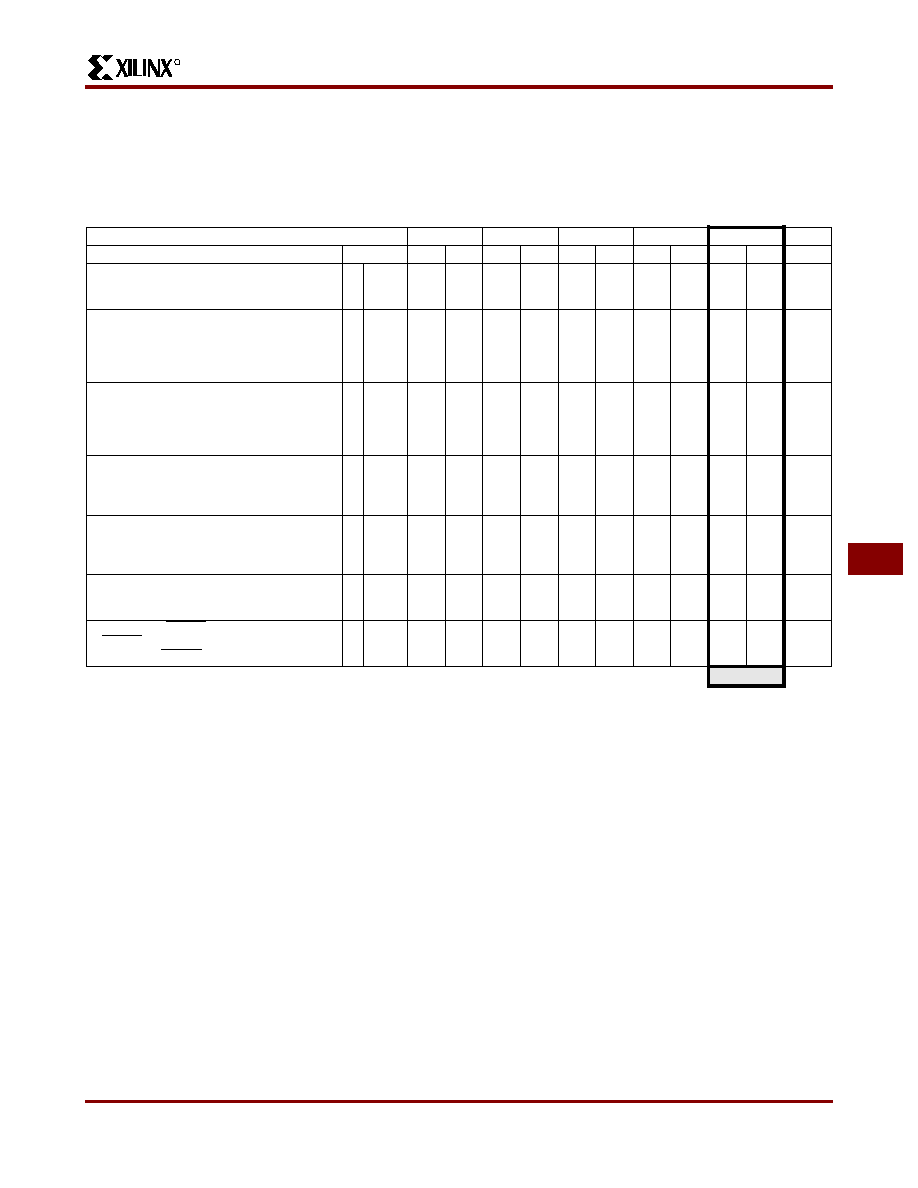
R
November 9, 1998 (Version 3.1)
7-55
XC3000 Series Field Programmable Gate Arrays
7
XC3100A CLB Switching Characteristics Guidelines
Testing of the switching parameters is modeled after testing methods specified by MIL-M-38510/605. All devices are 100%
functionally tested. Since many internal timing parameters cannot be measured directly, they are derived from benchmark
timing patterns. The following guidelines reflect worst-case values over the recommended operating conditions. For more
detailed, more precise, and more up-to-date timing information, use the values provided by the timing calculator and used
in the simulator.
Notes:
1. The CLB K to Q output delay (T
CKO
, #8) of any CLB, plus the shortest possible interconnect delay, is always longer than the
Data In hold time requirement (T
CKDI
, #5) of any CLB on the same die.
2. T
ILO
, T
QLO
and T
ICK
are specified for 4-input functions. For 5-input functions or base FGM functions, each of these
specifications for the XC3100A family increases by 0.50 ns (-5), 0.42 ns (-4) and 0.35 ns (-3), 0.35 ns (-2), 0.30 ns (-1), and
0.30 ns (-09).
Speed Grade
-4
-3
-2
-1
-09
Description
Symbol
Min
Max
Min
Max
Min
Max
Min
Max
Min
Max
Units
Combinatorial Delay
Logic Variables
A, B, C, D, E,
to outputs X or Y
1
T
ILO
3.3
2.7
2.2
1.75
1.5
ns
Sequential delay
Clock k to outputs X or Y
Clock k to outputs X or Y when Q is returned
through function generators F or G to drive
X or Y
8
T
CKO
T
QLO
2.5
5.2
2.1
4.3
1.7
3.5
1.4
3.1
1.25
2.7
ns
ns
Set-up time before clock K
Logic Variables
A, B, C, D, E
Data In
DI
Enable Clock
EC
Reset Direct inactive
RD
2
4
6
T
ICK
T
DICK
T
ECCK
2.5
1.6
3.2
1.0
2.1
1.4
2.7
1.0
1.8
1.3
2.5
1.0
1.7
1.2
2.3
1.0
1.5
1.0
2.05
1.0
ns
ns
ns
ns
Hold Time after clock K
Logic Variables
A, B, C, D, E
Data In
DI
Enable Clock
EC
3
5
7
T
CKI
T
CKDI
T
CKEC
0
1.0
0.8
0
0.9
0.7
0
0.9
0.7
0
0.8
0.6
0
0.7
0.55
ns
ns
ns
Clock
Clock High time
Clock Low time
Max. flip-flop toggle rate
11
12
T
CH
T
CL
F
CLK
2.0
2.0
227
1.6
1.6
270
1.3
1.3
323
1.3
1.3
323
1.3
1.3
370
ns
ns
MHz
Reset Direct (RD)
RD width
delay from RD to outputs X or Y
13
9
T
RPW
T
RIO
3.2
3.7
2.7
3.1
2.3
2.7
2.3
2.4
2.05
2.15
ns
ns
Global Reset (RESET Pad)
1
RESET width (Low)
(XC3142A)
delay from RESET pad to outputs X or Y
T
MRW
T
MRQ
14.0
14.0
12.0
12.0
12.0
12.0
12.0
12.0
12.0
12.0
ns
ns
Prelim

R
XC3000 Series Field Programmable Gate Arrays
7-56
November 9, 1998 (Version 3.1)
XC3100A CLB Switching Characteristics Guidelines (continued)
1
T
ILO
CLB Output (X, Y)
(Combinatorial)
CLB Input (A,B,C,D,E)
CLB Clock
CLB Input
(Direct In)
CLB Input
(Enable Clock)
CLB Output
(Flip-Flop)
CLB Input
(Reset Direct)
CLB Output
(Flip-Flop)
8
T
CKO
X5424
13 T
T
RPW
9
T
RIO
4
T
DICK
6
T
ECCK
12 T
CL
2
T
ICK
3
T
CKI
11 T
CH
5
T
CKDI
7
T
CKEC
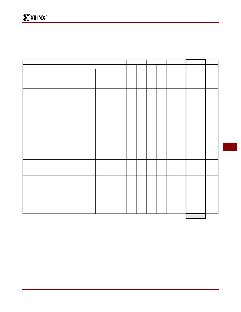
R
November 9, 1998 (Version 3.1)
7-57
XC3000 Series Field Programmable Gate Arrays
7
XC3100A IOB Switching Characteristics Guidelines
Testing of the switching parameters is modeled after testing methods specified by MIL-M-38510/605. All devices are 100%
functionally tested. Since many internal timing parameters cannot be measured directly, they are derived from benchmark
timing patterns. The following guidelines reflect worst-case values over the recommended operating conditions. For more
detailed, more precise, and more up-to-date timing information, use the values provided by the timing calculator and used
in the simulator.
Notes:
1. Timing is measured at pin threshold, with 50 pF external capacitive loads (incl. test fixture). For larger capacitive loads, see
XAPP024. Typical slew rate limited output rise/fall times are approximately four times longer.
2. Voltage levels of unused (bonded and unbonded) pads must be valid logic levels. Each can be configured with the internal
pull-up resistor or alternatively configured as a driven output or driven from an external source.
3. Input pad set-up time is specified with respect to the internal clock (ik). In order to calculate system set-up time, subtract
clock delay (pad to ik) from the input pad set-up time value. Input pad holdtime with respect to the internal clock (ik) is
negative. This means that pad level changes immediately before the internal clock edge (ik) will not be recognized.
4. T
PID
, T
PTG
, and T
PICK
are 3 ns higher for XTL2 when the pin is configured as a user input.
Speed Grade
-4
-3
-2
-1
-09
Description
Symbol
Min
Max
Min
Max
Min
Max
Min
Max
Min
Max
Units
Propagation Delays (Input)
Pad to Direct In (I)
Pad to Registered In (Q)
with latch transparent(XC3100A)Clock (IK)
to Registered In (Q)
3
4
T
PID
T
PTG
T
IKRI
2.5
12.0
2.5
2.2
11.0
2.2
2.0
11.0
1.9
1.7
10.0
1.7
1.55
9.2
1.55
ns
ns
ns
Set-up Time (Input)
Pad to Clock (IK) set-up time
XC3120A, XC3130A
XC3142A
XC3164A
XC3190A
XC3195A
1
T
PICK
10.6
10.7
11.0
11.2
11.6
9.4
9.5
9.7
9.9
10.3
8.9
9.0
9.2
9.4
9.8
8.0
8.1
8.3
8.5
8.9
7.2
7.3
7.5
7.7
8.1
ns
ns
ns
ns
ns
Propagation Delays (Output)
Clock (OK) to Pad
(fast)
same
(slew rate limited)
Output (O) to Pad
(fast)
same
(slew-rate limited)
(XC3100A)
3-state to Pad
begin hi-Z
(fast)
same
(slew-rate limited)
3-state to Pad
active and valid (fast) (XC3100A)
same
(slew -rate limited)
7
7
10
10
9
9
8
8
T
OKPO
T
OKPO
T
OPF
T
OPS
T
TSHZ
T
TSHZ
T
TSON
T
TSON
5.0
12.0
3.7
11.0
6.2
6.2
10.0
17.0
4.4
10.0
3.3
9.0
5.5
5.5
9.0
15.0
3.7
9.7
3.0
8.7
5.0
5.0
8.5
14.2
3.4
8.4
3.0
8.0
4.5
4.5
6.5
11.5
3.3
6.9
2.9
6.5
4.05
4.05
5.0
8.6
ns
ns
ns
ns
ns
ns
ns
ns
ns
Set-up and Hold Times (Output)
Output (O) to clock (OK) set-up time
(XC3100A)
Output (O) to clock (OK) hold time
5
6
T
OOK
T
OKO
4.5
0
3.6
0
3.2
0
2.9
ns
ns
Clock
Clock High time
Clock Low time
Max. flip-flop toggle rate
11
12
T
IOH
T
IOL
F
CLK
2.0
2.0
227
1.6
1.6
270
1.3
1.3
323
1.3
1.3
323
1.3
1.3
370
ns
ns
MHz
Global Reset Delays
RESET Pad to Registered In
(Q)
(XC3142A)
(XC3190A)
RESET Pad to output pad
(fast)
(slew-rate limited)
13
15
15
T
RRI
T
RPO
T
RPO
15.0
25.5
20.0
27.0
13.0
21.0
17.0
23.0
13.0
21.0
17.0
23.0
13.0
21.0
17.0
22.0
14.4
21.0
17.0
21.0
ns
ns
ns
ns
Preliminary

R
XC3000 Series Field Programmable Gate Arrays
7-58
November 9, 1998 (Version 3.1)
XC3100A IOB Switching Characteristics Guidelines (continued)
3
T
PID
I/O Block (I)
I/O Pad Input
I/O Clock (IK/OK)
I/O Block (RI)
RESET
I/O Block (O)
I/O Pad TS
I/O Pad Output
I/O Pad Output
(Direct)
I/O Pad Output
(Registered)
X5425
5
T
OOK
12 T
IOL
1
T
PICK
11 T
IOH
4
T
IKRI
15 T
RPO
13 T
RRI
6
T
OKO
9
T
TSHZ
10 T
OP
7
T
OKPO
8
T
TSON
FLIP
FLOP
Q
D
R
SLEW
RATE
PASSIVE
PULL UP
OUTPUT
SELECT
3-STATE
INVERT
OUT
INVERT
FLIP
FLOP
or
LATCH
D
Q
R
REGISTERED IN
DIRECT IN
OUT
3- STATE
(OUTPUT ENABLE)
TTL or
CMOS
INPUT
THRESHOLD
OUTPUT
BUFFER
(GLOBAL RESET)
CK1
X3029
I/O PAD
Vcc
PROGRAM-CONTROLLED MEMORY CELLS
PROGRAMMABLE INTERCONNECTION POINT or PIP
=
IK
OK
Q
I
O
T
PROGRAM
CONTROLLED
MULTIPLEXER
CK2
R
November 9, 1998 (Version 3.1)
7-59
XC3000 Series Field Programmable Gate Arrays
7
XC3100L Switching Characteristics
Xilinx maintains test specifications for each product as controlled documents. To insure the use of the most recently released
device performance parameters, please request a copy of the current test-specification revision.
XC3100L Operating Conditions
Notes:
1. At junction temperatures above those listed as Operating Conditions, all delay parameters increase by 0.3% per
�
C.
2. Although the present (1996) devices operate over the full supply voltage range from 3.0 V to 5.25 V, Xilinx reserves the right
to restrict operation to the 3.0 and 3.6 V range later, when smaller device geometries might preclude operation @ 5 V.
Operating conditions are guaranteed in the 3.0 � 3.6 V V
CC
range.
XC3100L DC Characteristics Over Operating Conditions
Notes:
1. With no output current loads, no active input or long line pull-up resistors, all package pins at V
CC
or GND, and the FPGA
configured with a tie option.
2. Total continuous output sink current may not exceed 100 mA per ground pin. Total continuous output source current may not
exceed 100 mA per V
CC
pin. The number of ground pins varies from the XC3142L to the XC3190L.
3. Not tested. Allows undriven pins to float High. For any other purpose, use an external pull-up.
Symbol
Description
Min
Max
Units
V
CC
Supply voltage relative to GND Commercial 0
�
C to +85
�
C junction
3.0
3.6
V
V
IH
High-level input voltage
2.0
V
CC
+ 0.3
V
V
IL
Low-level input voltage
-0.3
0.8
V
T
IN
Input signal transition time
250
ns
Symbol
Description
Min
Max
Units
V
OH
High-level output voltage (@ I
OH
= -4.0 mA, V
CC
min)
2.4
V
High-level output voltage (@ I
OH
= -100.0
�
A, V
CC
min)
V
CC
-0.2
V
V
OL
Low-level output voltage (@ I
OH
= 4.0 mA, V
CC
min)
0.40
V
Low-level output voltage (@ I
OH
= +100.0
�
A, V
CC
min)
0.2
V
V
CCPD
Power-down supply voltage (PWRDWN must be Low)
2.30
V
I
CCO
Quiescent FPGA supply current
Chip thresholds programmed as CMOS levels
1
1.5
mA
I
IL
Input Leakage Current
-10
+10
�
A
C
IN
Input capacitance
(sample tested)
All pins except XTL1 and XTL2
XTL1 and XTL2
10
15
pF
pF
I
RIN
Pad pull-up (when selected) @ V
IN
= 0 V
3
0.02
0.17
mA
I
RLL
Horizontal long line pull-up (when selected) @ logic Low
0.20
2.80
mA
R
XC3000 Series Field Programmable Gate Arrays
7-60
November 9, 1998 (Version 3.1)
XC3100L Absolute Maximum Ratings
Note:
Stresses beyond those listed under Absolute Maximum Ratings may cause permanent damage to the device. These are
stress ratings only, and functional operation of the device at these or any other conditions beyond those listed under
Recommended Operating Conditions is not implied. Exposure to Absolute Maximum Ratings conditions for extended
periods of time may affect device reliability.
XC3100L Global Buffer Switching Characteristics Guidelines
Notes:
1. Timing is based on the XC3142L, for other devices see timing calculator.
2. The use of two pull-up resistors per longline, available on other XC3000 devices, is not a valid option for XC3100L devices.
Symbol
Description
Units
V
CC
Supply voltage relative to GND
�0.5 to +7.0
V
V
IN
Input voltage with respect to GND
�0.5 to V
CC
+0.5
V
V
TS
Voltage applied to 3-state output
�0.5 to V
CC
+0.5
V
T
STG
Storage temperature (ambient)
�65 to +150
�
C
T
SOL
Maximum soldering temperature (10 s @ 1/16 in.)
+260
�
C
T
J
Junction temperature plastic
+125
�
C
Junction temperature ceramic
+150
�
C
Speed Grade
-3
-2
Description
Symbol
Max
Max
Units
Global and Alternate Clock Distribution
1
Either:Normal IOB input pad through clock buffer
to any CLB or IOB clock input
Or: Fast (CMOS only) input pad through clock
buffer to any CLB or IOB clock input
T
PID
T
PIDC
5.6
4.3
4.7
3.7
ns
ns
TBUF driving a Horizontal Longline (L.L.)
1
I to L.L. while T is Low (buffer active)
T
to L.L. active and valid with single pull-up resistor
T
to L.L. High with single pull-up resistor
T
IO
T
ON
T
PUS
3.1
4.2
11.4
3.1
4.2
11.4
ns
ns
ns
BIDI
Bidirectional buffer delay
T
BIDI
1.0
0.9
ns
Advance

R
November 9, 1998 (Version 3.1)
7-61
XC3000 Series Field Programmable Gate Arrays
7
XC3100L CLB Switching Characteristics Guidelines
Testing of the switching parameters is modeled after testing methods specified by MIL-M-38510/605. All devices are 100%
functionally tested. Since many internal timing parameters cannot be measured directly, they are derived from benchmark
timing patterns. The following guidelines reflect worst-case values over the recommended operating conditions. For more
detailed, more precise, and more up-to-date timing information, use the values provided by the timing calculator and used
in the simulator.
Notes:
1. The CLB K to Q delay (T
CKO
, #8) of any CLB, plus the shortest possible interconnect delay, is always longer than the Data
In hold time requirement (T
CKDI
, #5) of any CLB on the same die.
2. T
ILO
, T
QLO
and T
ICK
are specified for 4-input functions. For 5-input functions or base FGM functions, each of these
specifications for the XC3100L family increase by 0.35 ns (-3) and 0.29 ns (-2).
Speed Grade
-3
-2
Description
Symbol
Min
Max
Min
Max
Units
Combinatorial Delay
Logic Variables A, B, C, D, E, to outputs X or Y
1
T
ILO
2.7
2.2
ns
Sequential delay
Clock k to outputs X or Y
Clock k to outputs X or Y when Q is returned
through function generators F or G to drive X or Y
8
T
CKO
T
QLO
2.1
4.3
1.7
3.5
ns
ns
Set-up time before clock K
Logic Variables
A, B, C, D, E
Data In
DI
Enable Clock
EC
Reset Direct Inactive
RD
2
4
6
T
ICK
T
DICK
T
ECCK
2.1
1.4
2.7
1.0
1.8
1.3
2.5
1.0
ns
ns
ns
ns
Hold Time after clock K
Logic Variables
A, B, C, D, E
Data In
DI
Enable Clock
EC
3
5
7
T
CKI
T
CKDI
T
CKEC
0
0.9
0.7
0
0.9
0.7
ns
ns
ns
Clock
Clock High time
Clock Low time
Max. flip-flop toggle rate
11
12
T
CH
T
CL
F
CLK
1.6
1.6
270
1.3
1.3
325
ns
ns
MHz
Reset Direct (RD)
RD width
delay from RD to outputs X or Y
13
9
T
RPW
T
RIO
2.7
3.1
2.3
2.7
ns
ns
Global Reset (RESET Pad)
RESET width (Low)
(XC3142L)
delay from RESET pad to outputs X or Y
T
MRW
T
MRQ
12.0
12.0
12.0
12.0
ns
ns
Advance
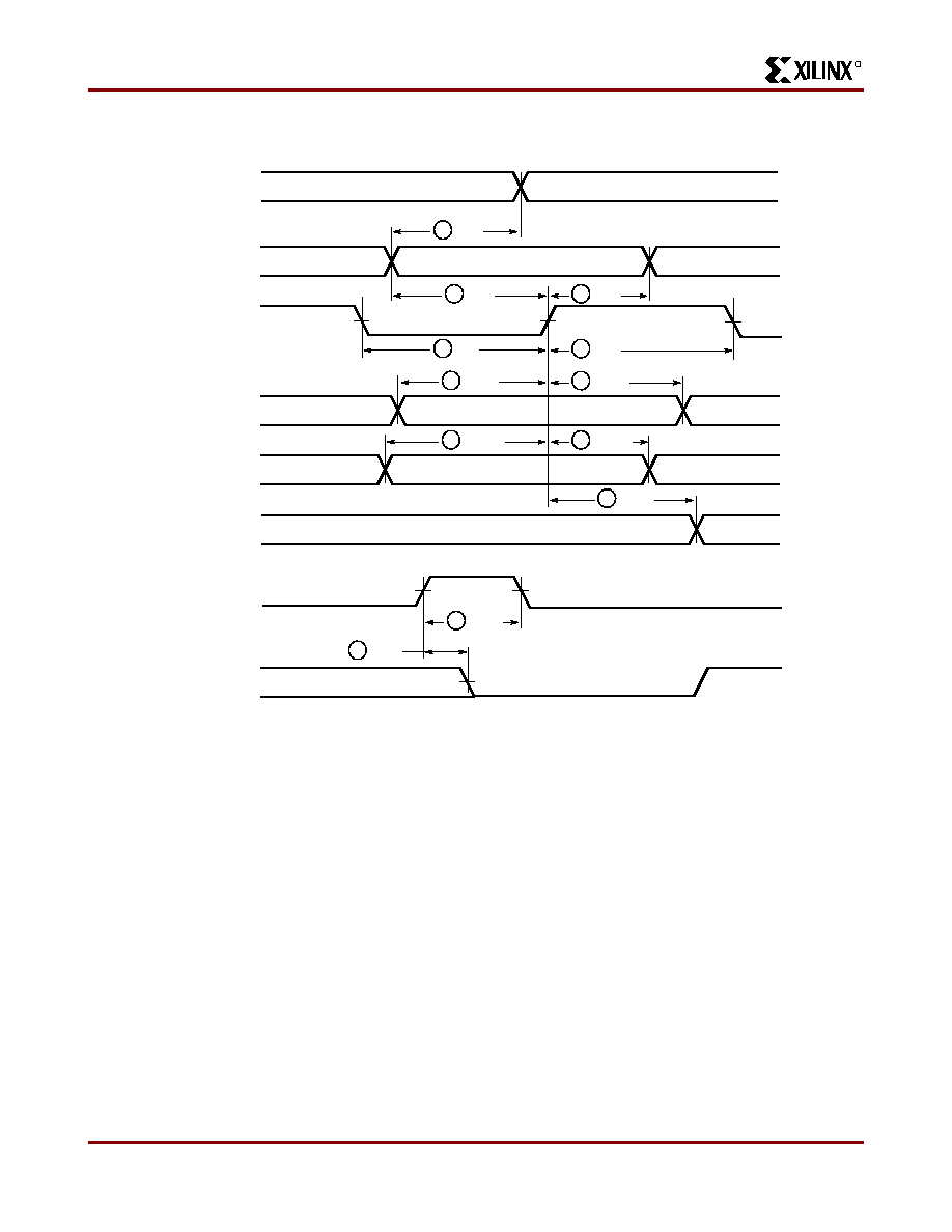
R
XC3000 Series Field Programmable Gate Arrays
7-62
November 9, 1998 (Version 3.1)
XC3100L CLB Switching Characteristics Guidelines (continued)
1
T
ILO
CLB Output (X, Y)
(Combinatorial)
CLB Input (A,B,C,D,E)
CLB Clock
CLB Input
(Direct In)
CLB Input
(Enable Clock)
CLB Output
(Flip-Flop)
CLB Input
(Reset Direct)
CLB Output
(Flip-Flop)
8
T
CKO
X5424
13 T
T
RPW
9
T
RIO
4
T
DICK
6
T
ECCK
12 T
CL
2
T
ICK
3
T
CKI
11 T
CH
5
T
CKDI
7
T
CKEC
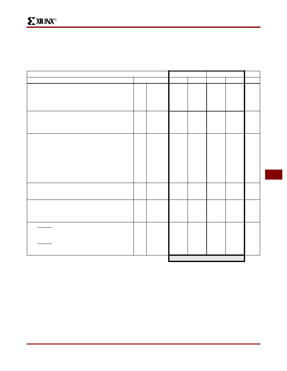
R
November 9, 1998 (Version 3.1)
7-63
XC3000 Series Field Programmable Gate Arrays
7
XC3100L IOB Switching Characteristics Guidelines
Testing of the switching parameters is modeled after testing methods specified by MIL-M-38510/605. All devices are 100%
functionally tested. Since many internal timing parameters cannot be measured directly, they are derived from benchmark
timing patterns. The following guidelines reflect worst-case values over the recommended operating conditions. For more
detailed, more precise, and more up-to-date timing information, use the values provided by the timing calculator and used
in the simulator.
Notes:
1. Timing is measured at pin threshold, with 50 pF external capacitive loads (incl. test fixture). Typical slew rate limited output
rise/fall times are approximately four times longer.
2. Voltage levels of unused (bonded and unbonded) pads must be valid logic levels. Each can be configured with the internal
pull-up resistor or alternatively configured as a driven output or driven from an external source.
3. Input pad set-up time is specified with respect to the internal clock (IK). In order to calculate system set-up time, subtract
clock delay (pad to ik) from the input pad set-up time value. Input pad holdtime with respect to the internal clock (IK) is
negative. This means that pad level changes immediately before the internal clock edge (IK) will not be recognized.
Speed Grade
-3
-2
Description
Symbol
Min
Max
Min
Max
Units
Propagation Delays (Input)
Pad to Direct In (I)
Pad to Registered In (Q) with latch (XC3100L)
transparent
Clock (IK) to Registered In (Q)
3
4
T
PID
T
PTG
T
IKRI
2.2
11.0
2.2
2.0
11.0
1.9
ns
ns
ns
Set-up Time (Input)
Pad to Clock (IK) set-up time
XC3142L
XC3190L
1
T
PICK
9.5
9.9
9.0
9.4
ns
ns
Propagation Delays (Output)
Clock (OK) to Pad
(fast)
same
(slew rate limited)
Output (O) to Pad
(fast)
same
(slew-rate limited)(XC3100L)
3-state to Pad begin hi-Z
(fast)
same
(slew-rate limited)
3-state to Pad active and valid (fast)(XC3100L)
same
(slew -rate limited)
7
7
10
10
9
9
8
8
T
OKPO
T
OK
PO
T
OPF
T
OPF
T
TSHZ
T
TSHZ
T
TSON
T
TSON
4.4
10.0
3.3
9.0
5.5
5.5
9.0
15.0
4.0
9.7
3.0
8.7
5.0
5.0
8.5
14.2
ns
ns
ns
ns
ns
ns
ns
ns
Set-up and Hold Times (Output)
Output (O) to clock (OK) set-up time (XC3100L)
Output (O) to clock (OK) hold time
5
6
T
OOK
T
OKO
4.0
0
3.6
0
ns
ns
Clock
Clock High time
Clock Low time
Export Control Maximum flip-flop toggle rate
11
12
T
IOH
T
IOL
F
TOG
1.6
1.6
270
1.3
1.3
325
ns
ns
MHz
Global Reset Delays
RESET Pad to Registered In (Q)
(XC3142L)
(XC3190L)
RESET Pad to output pad
(fast)
(slew-rate limited)
13
15
15
T
RRI
T
RPO
T
RPO
16.0
21.0
17.0
23.0
16.0
21.0
17.0
23.0
ns
ns
ns
ns
Advance
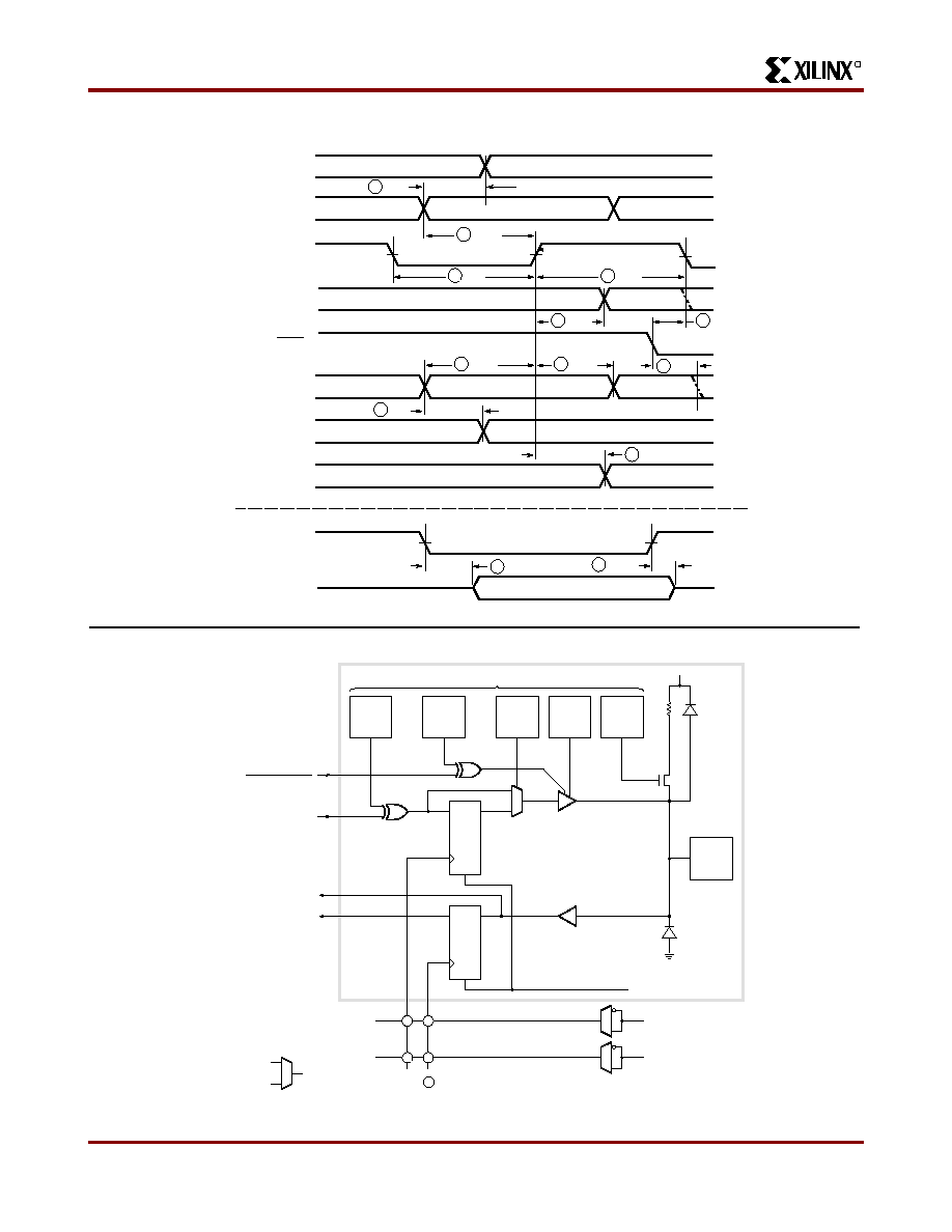
R
XC3000 Series Field Programmable Gate Arrays
7-64
November 9, 1998 (Version 3.1)
XC3100L IOB Switching Characteristics Guidelines (continued)
3
T
PID
I/O Block (I)
I/O Pad Input
I/O Clock (IK/OK)
I/O Block (RI)
RESET
I/O Block (O)
I/O Pad TS
I/O Pad Output
I/O Pad Output
(Direct)
I/O Pad Output
(Registered)
X5425
5
T
OOK
12 T
IOL
1
T
PICK
11 T
IOH
4
T
IKRI
15 T
RPO
13 T
RRI
6
T
OKO
9
T
TSHZ
10 T
OP
7
T
OKPO
8
T
TSON
FLIP
FLOP
Q
D
R
SLEW
RATE
PASSIVE
PULL UP
OUTPUT
SELECT
3-STATE
INVERT
OUT
INVERT
FLIP
FLOP
or
LATCH
D
Q
R
REGISTERED IN
DIRECT IN
OUT
3- STATE
(OUTPUT ENABLE)
TTL or
CMOS
INPUT
THRESHOLD
OUTPUT
BUFFER
(GLOBAL RESET)
CK1
X3029
I/O PAD
Vcc
PROGRAM-CONTROLLED MEMORY CELLS
PROGRAMMABLE INTERCONNECTION POINT or PIP
=
IK
OK
Q
I
O
T
PROGRAM
CONTROLLED
MULTIPLEXER
CK2

R
November 9, 1998 (Version 3.1)
7-65
XC3000 Series Field Programmable Gate Arrays
7
XC3000 Series Pin Assignments
Xilinx offers the six different array sizes in the XC3000 families in a variety of surface-mount and through-hole package
types, with pin counts from 44 to 208.
Each chip is offered in several package types to accommodate the available PC board space and manufacturing technology.
Most package types are also offered with different chips to accommodate design changes without the need for PC board
changes.
Note that there is no perfect match between the number of bonding pads on the chip and the number of pins on a package.
In some cases, the chip has more pads than there are pins on the package, as indicated by the information ("unused" pads)
below the line in the following table. The IOBs of the unconnected pads can still be used as storage elements if the specified
propagation delays and set-up times are acceptable.
In other cases, the chip has fewer pads than there are pins on the package; therefore, some package pins are not connected
(n.c.), as shown above the line in the following table.
XC3000 Series 44-Pin PLCC Pinouts
XC3000A, XC3000L, and XC3100A families have identical pinouts
Peripheral mode and Master Parallel mode are not supported in the PC44 package
Pin No.
XC3030A
Pin No.
XC3030A
1
GND
23
GND
2
I/O
24
I/O
3
I/O
25
I/O
4
I/O
26
XTL2(IN)-I/O
5
I/O
27
RESET
6
I/O
28
DONE-PGM
7
PWRDWN
29
I/O
8
TCLKIN-I/O
30
XTL1(OUT)-BCLK-I/O
9
I/O
31
I/O
10
I/O
32
I/O
11
I/O
33
I/O
12
VCC
34
VCC
13
I/O
35
I/O
14
I/O
36
I/O
15
I/O
37
I/O
16
M1-RDATA
38
DIN-I/O
17
M0-RTRIG
39
DOUT-I/O
18
M2-I/O
40
CCLK
19
HDC-I/O
41
I/O
20
LDC-I/O
42
I/O
21
I/O
43
I/O
22
INIT-I/O
44
I/O

R
XC3000 Series Field Programmable Gate Arrays
7-66
November 9, 1998 (Version 3.1)
XC3000 Series 64-Pin Plastic VQFP Pinouts
XC3000A, XC3000L, and XC3100A families have identical pinouts
Pin No.
XC3030A
Pin No.
XC3030A
1
A0-WS-I/O
33
M2-I/O
2
A1-CS2-I/O
34
HDC-I/O
3
A2-I/O
35
I/O
4
A3-I/O
36
LDC-I/O
5
A4-I/O
37
I/O
6
A14-I/O
38
I/O
7
A5-I/O
39
I/O
8
GND
40
INIT-I/O
9
A13-I/O
41
GND
10
A6-I/O
42
I/O
11
A12-I/O
43
I/O
12
A7-I/O
44
I/O
13
A11-I/O
45
I/O
14
A8-I/O
46
I/O
15
A10-I/O
47
XTAL2(IN)-I/O
16
A9-I/O
48
RESET
17
PWRDN
49
DONE-PG
18
TCLKIN-I/O
50
D7-I/O
19
I/O
51
XTAL1(OUT)-BCLKIN-I/O
20
I/O
52
D6-I/O
21
I/O
53
D5-I/O
22
I/O
54
CS0-I/O
23
I/O
55
D4-I/O
24
VCC
56
VCC
25
I/O
57
D3-I/O
26
I/O
58
CS1-I/O
27
I/O
59
D2-I/O
28
I/O
60
D1-I/O
29
I/O
61
RDY/BUSY-RCLK-I/O
30
I/O
62
D0-DIN-I/O
31
M1-RDATA
63
DOUT-I/O
32
M0-RTRIG
64
CCLK
R
November 9, 1998 (Version 3.1)
7-67
XC3000 Series Field Programmable Gate Arrays
7
XC3000 Series 68-Pin PLCC, 84-Pin PLCC and PGA Pinouts
XC3000A, XC3000L, XC3100A, and XC3100L families have identical pinouts
Unprogrammed IOBs have a default pull-up. This prevents an undefined pad level for unbonded or unused IOBs.
Programmed outputs are default slew-rate limited.
This table describes the pinouts of three different chips in three different packages. The pin-description column lists 84 of the
118 pads on the XC3042A (and 84 of the 98 pads on the XC3030A) that are connected to the 84 package pins. Ten pads,
indicated by an asterisk, do not exist on the XC3020A, which has 74 pads; therefore the corresponding pins on the 84-pin
packages have no connections to an XC3020A. Six pads on the XC3020A and 16 pads on the XC3030A, indicated by a
dash (--) in the 68 PLCC column, have no connection to the 68 PLCC, but are connected to the 84-pin packages.
68 PLCC
XC3020A, XC3030A,
XC3042A
84 PLCC
68 PLCC
XC3020A, XC3030A,
XC3042A
84 PLCC
XC3030A XC3020A
XC3030A XC3020A
10
10
PWRDN
12
44
44
RESET
54
11
11
TCLKIN-I/O
13
45
45
DONE-PG
55
12
--
I/O*
14
46
46
D7-I/O
56
13
12
I/O
15
47
47
XTL1(OUT)-BCLKIN-I/O
57
14
13
I/O
16
48
48
D6-I/O
58
--
--
I/O
17
--
--
I/O
59
15
14
I/O
18
49
49
D5-I/O
60
16
15
I/O
19
50
50
CS0-I/O
61
--
16
I/O
20
51
51
D4-I/O
62
17
17
I/O
21
--
--
I/O
63
18
18
VCC
22
52
52
VCC
64
19
19
I/O
23
53
53
D3-I/O
65
--
--
I/O
24
54
54
CS1-I/O
66
20
20
I/O
25
55
55
D2-I/O
67
--
21
I/O
26
--
--
I/O
68
21
22
I/O
27
--
--
I/O*
69
22
--
I/O
28
56
56
D1-I/O
70
23
23
I/O
29
57
57
RDY/BUSY-RCLK-I/O
71
24
24
I/O
30
58
58
D0-DIN-I/O
72
25
25
M1-RDATA
31
59
59
DOUT-I/O
73
26
26
M0-RTRIG
32
60
60
CCLK
74
27
27
M2-I/O
33
61
61
A0-WS-I/O
75
28
28
HDC-I/O
34
62
62
A1-CS2-I/O
76
29
29
I/O
35
63
63
A2-I/O
77
30
30
LDC-I/O
36
64
64
A3-I/O
78
-- 31
I/O
37
--
--
I/O*
79
-- I/O*
38
--
--
I/O*
80
31
32
I/O
39
65
65
A15-I/O
81
32
33
I/O
40
66
66
A4-I/O
82
33
--
I/O*
41
67
67
A14-I/O
83
34
34
INIT-I/O
42
68
68
A5-I/O
84
35
35
GND
43
1
1
GND
1
36
36
I/O
44
2
2
A13-I/O
2
37
37
I/O
45
3
3
A6-I/O
3
38
38
I/O
46
4
4
A12-I/O
4
39
39
I/O
47
5
5
A7-I/O
5
-- 40
I/O
48
--
--
I/O*
6
-- 41
I/O
49
--
--
I/O*
7
40
I/O*
50
6
6
A11-I/O
8
41
I/O*
51
7
7
A8-I/O
9
42
42
I/O
52
8
8
A10-I/O
10
43
43
XTL2(IN)-I/O
53
9
9
A9-I/O
11
R
XC3000 Series Field Programmable Gate Arrays
7-68
November 9, 1998 (Version 3.1)
XC3064A/XC3090A/XC3195A 84-Pin PLCC Pinouts
XC3000A, XC3000L, XC3100A, and XC3100L families have identical pinouts
Unprogrammed IOBs have a default pull-up. This prevents an undefined pad level for unbonded or unused IOBs.
Programmed outputs are default slew-rate limited.
* In the PC84 package, XC3064A, XC3090A and XC3195A have additional VCC and GND pins and thus a different pin
definition than XC3020A/XC3030A/XC3042A.
PLCC Pin Number
XC3064A, XC3090A, XC3195A
PLCC Pin Number
XC3064A, XC3090A, XC3195A
12
PWRDN
54
RESET
13
TCLKIN-I/O
55
DONE-PG
14
I/O
56
D7-I/O
15
I/O
57
XTL1(OUT)-BCLKIN-I/O
16
I/O
58
D6-I/O
17
I/O
59
I/O
18
I/O
60
D5-I/O
19
I/O
61
CS0-I/O
20
I/O
62
D4-I/O
21
GND*
63
I/O
22
VCC
64
VCC
23
I/O
65
GND*
24
I/O
66
D3-I/O*
25
I/O
67
CS1-I/O*
26
I/O
68
D2-I/O*
27
I/O
69
I/O
28
I/O
70
D1-I/O
29
I/O
71
RDY/BUSY-RCLK-I/O
30
I/O
72
D0-DIN-I/O
31
M1-RDATA
73
DOUT-I/O
32
M0-RTRIG
74
CCLK
33
M2-I/O
75
A0-WS-I/O
34
HDC-I/O
76
A1-CS2-I/O
35
I/O
77
A2-I/O
36
LDC-I/O
78
A3-I/O
37
I/O
79
I/O
38
I/O
80
I/O
39
I/O
81
A15-I/O
40
I/O
82
A4-I/O
41
INIT/I/O*
83
A14-I/O
42
VCC*
84
A5-I/O
43
GND
1
GND
44
I/O
2
VCC*
45
I/O
3
A13-I/O*
46
I/O
4
A6-I/O*
47
I/O
5
A12-I/O*
48
I/O
6
A7-I/O*
49
I/O
7
I/O
50
I/O
8
A11-I/O
51
I/O 9
A8-I/O
52
I/O
10
A10-I/O
53
XTL2(IN)-I/O
11
A9-I/O

R
November 9, 1998 (Version 3.1)
7-69
XC3000 Series Field Programmable Gate Arrays
7
XC3000 Series 100-Pin QFP Pinouts
XC3000A, XC3000L, XC3100A, and XC3100L families have identical pinouts
Unprogrammed IOBs have a default pull-up. This prevents an undefined pad level for unbonded or unused IOBs.
Programmed outputs are default slew-rate limited.
* This table describes the pinouts of three different chips in three different packages. The pin-description column lists 100 of
the 118 pads on the XC3042A that are connected to the 100 package pins. Two pads, indicated by double asterisks, do not
exist on the XC3030A, which has 98 pads; therefore the corresponding pins have no connections. Twenty-six pads,
indicated by single or double asterisks, do not exist on the XC3020A, which has 74 pads; therefore, the corresponding pins
have no connections. (See table on
page 65
.)
Pin No.
XC3020A
XC3030A
XC3042A
Pin No.
XC3020A
XC3030A
XC3042A
Pin No.
XC3020A
XC3030A
XC3042A
PQFP
TQFP
VQFP
PQFP
TQFP
VQFP
PQFP
TQFP
VQFP
16
13
GND
50
47
I/O*
84
81
I/O*
17
14
A13-I/O
51
48
I/O*
85
82
I/O*
18
15
A6-I/O
52
49
M1-RD
86
83
I/O
19
16
A12-I/O
53
50
GND*
87
84
D5-I/O
20
17
A7-I/O
54
51
MO-RT
88
85
CS0-I/O
21
18
I/O*
55
52
VCC*
89
86
D4-I/O
22
19
I/O*
56
53
M2-I/O
90
87
I/O
23
20
A11-I/O
57
54
HDC-I/O
91
88
VCC
24
21
A8-I/O
58
55
I/O
92
89
D3-I/O
25
22
A10-I/O
59
56
LDC-I/O
93
90
CS1-I/O
26
23
A9-I/O
60
57
I/O*
94
91
D2-I/O
27
24
VCC*
61
58
I/O*
95
92
I/O
28
25
GND*
62
59
I/O
96
93
I/O*
29
26
PWRDN
63
60
I/O
97
94
I/O*
30
27
TCLKIN-I/O
64
61
I/O
98
95
D1-I/O
31
28
I/O**
65
62
INIT-I/O
99
96
RDY/BUSY-RCLK-I/O
32
29
I/O*
66
63
GND
100
97
DO-DIN-I/O
33
30
I/O*
67
64
I/O
1
98
DOUT-I/O
34
31
I/O
68
65
I/O
2
99
CCLK
35
32
I/O
69
66
I/O
3
100
VCC*
36
33
I/O
70
67
I/O
4
1
GND*
37
34
I/O
71
68
I/O
5
2
AO-WS-I/O
38
35
I/O
72
69
I/O
6
3
A1-CS2-I/O
39
36
I/O
73
70
I/O
7
4
I/O**
40
37
I/O
74
71
I/O*
8
5
A2-I/O
41
38
VCC
75
72
I/O*
9
6
A3-I/O
42
39
I/O
76
73
XTL2-I/O
10
7
I/O*
43
40
I/O
77
74
GND*
11
8
I/O*
44
41
I/O
78
75
RESET
12
9
A15-I/O
45
42
I/O
79
76
VCC*
13
10
A4-I/O
46
43
I/O
80
77
DONE-PG
14
11
A14-I/O
47
44
I/O
81
78
D7-I/O
15
12
A5-I/O
48
45
I/O
82
79
BCLKIN-XTL1-I/O
49
46
I/O
83
80
D6-I/O

R
XC3000 Series Field Programmable Gate Arrays
7-70
November 9, 1998 (Version 3.1)
XC3000 Series 132-Pin Ceramic and Plastic PGA Pinouts
XC3000A, XC3000L, XC3100A, and XC3100L families have identical pinouts
Unprogrammed IOBs have a default pull-up. This prevents an undefined pad level for unbonded or unused IOBs.
Programmed outputs are default slew-rate limited.
* Indicates unconnected package pins (14) for the XC3042A.
PGA
Pin
Number
XC3042A
XC3064A
PGA
Pin
Number
XC3042A
XC3064A
PGA
Pin
Number
XC3042A
XC3064A
PGA
Pin
Number
XC3042A
XC3064A
C4
GND
B13
M1-RD
P14
RESET
M3
DOUT-I/O
A1
PWRDN
C11
GND
M11
VCC
P1
CCLK
C3
I/O-TCLKIN
A14
M0-RT
N13
DONE-PG
M4
VCC
B2
I/O
D12
VCC
M12
D7-I/O
L3
GND
B3
I/O
C13
M2-I/O
P13
XTL1-I/O-BCLKIN
M2
A0-WS-I/O
A2
I/O*
B14
HDC-I/O
N12
I/O
N1
A1-CS2-I/O
B4
I/O
C14
I/O
P12
I/O
M1
I/O
C5
I/O
E12
I/O
N11
D6-I/O
K3
I/O
A3
I/O*
D13
I/O
M10
I/O
L2
A2-I/O
A4
I/O
D14
LDC-I/O
P11
I/O*
L1
A3-I/O
B5
I/O
E13
I/O*
N10
I/O
K2
I/O
C6
I/O
F12
I/O
P10
I/O
J3
I/O
A5
I/O
E14
I/O
M9
D5-I/O
K1
A15-I/O
B6
I/O
F13
I/O
N9
CS0-I/O
J2
A4-I/O
A6
I/O
F14
I/O
P9
I/O*
J1
I/O*
B7
I/O
G13
I/O
P8
I/O*
H1
A14-I/O
C7
GND
G14
INIT-I/O
N8
D4-I/O
H2
A5-I/O
C8
VCC
G12
VCC
P7
I/O
H3
GND
A7
I/O
H12
GND
M8
VCC
G3
VCC
B8
I/O
H14
I/O
M7
GND
G2
A13-I/O
A8
I/O
H13
I/O
N7
D3-I/O
G1
A6-I/O
A9
I/O
J14
I/O
P6
CS1-I/O
F1
I/O*
B9
I/O
J13
I/O
N6
I/O*
F2
A12-I/O
C9
I/O
K14
I/O
P5
I/O*
E1
A7-I/O
A10
I/O
J12
I/O
M6
D2-I/O
F3
I/O
B10
I/O
K13
I/O
N5
I/O
E2
I/O
A11
I/O*
L14
I/O*
P4
I/O
D1
A11-I/O
C10
I/O
L13
I/O
P3
I/O
D2
A8-I/O
B11
I/O
K12
I/O
M5
D1-I/O
E3
I/O
A12
I/O*
M14
I/O
N4
RDY/BUSY-RCLK-I/O
C1
I/O
B12
I/O
N14
I/O
P2
I/O
B1
A10-I/O
A13
I/O*
M13
XTL2(IN)-I/O
N3
I/O
C2
A9-I/O
C12
I/O
L12
GND
N2
D0-DIN-I/O
D3
VCC
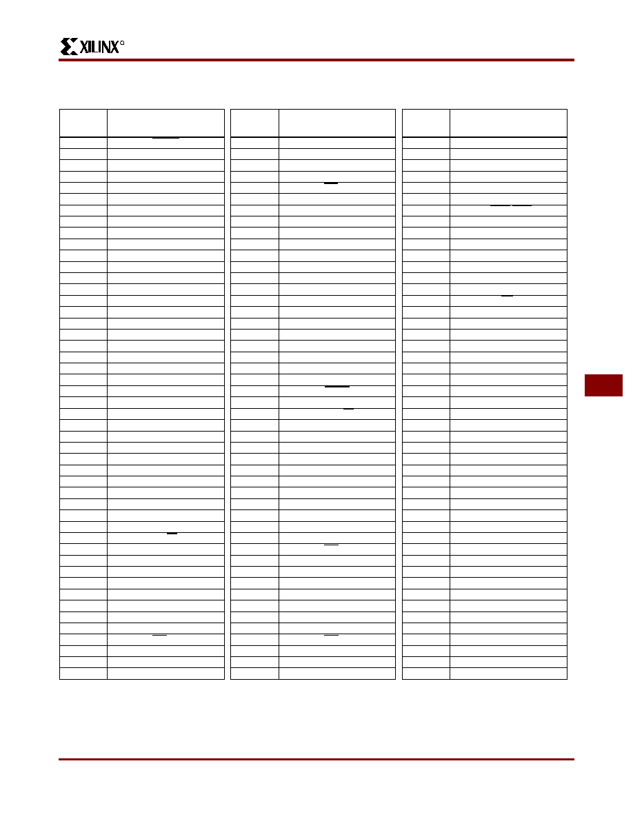
R
November 9, 1998 (Version 3.1)
7-71
XC3000 Series Field Programmable Gate Arrays
7
XC3000 Series 144-Pin Plastic TQFP Pinouts
XC3000A, XC3000L, XC3100A, and XC3100L families have identical pinouts
Unprogrammed IOBs have a default pull-up. This prevents an undefined pad level for unbonded or unused IOBs.
Programmed outputs are default slew-rate limited.
* Indicates unconnected package pins (24) for the XC3042A.
Pin
Number
XC3042A
XC3064A
XC3090A
Pin
Number
XC3042A
XC3064A
XC3090A
Pin
Number
XC3042A
XC3064A
XC3090A
1
PWRDN
49
I/O
97
I/O
2
I/O-TCLKIN
50
I/O*
98
I/O
3
I/O*
51
I/O
99
I/O*
4
I/O
52
I/O
100
I/O
5
I/O
53
INIT-I/O
101
I/O*
6
I/O*
54
VCC
102
D1-I/O
7
I/O
55
GND
103
RDY/BUSY-RCLK-I/O
8
I/O
56
I/O
104
I/O
9
I/O*
57
I/O
105
I/O
10
I/O
58
I/O
106
D0-DIN-I/O
11
I/O
59
I/O
107
DOUT-I/O
12
I/O
60
I/O
108
CCLK
13
I/O
61
I/O
109
VCC
14
I/O
62
I/O
110
GND
15
I/O*
63
I/O*
111
A0-WS
-I/
O
16
I/O
64
I/O*
112
A1-CS2-I/O
17
I/O
65
I/O
113
I/O
18
GND
66
I/O
114
I/O
19
VCC
67
I/O
115
A2-I/O
20
I/O
68
I/O
116
A3-I/O
21
I/O
69
XTL2(IN)-I/O
117
I/O
22
I/O
70
GND
118
I/O
23
I/O
71
RESET
119
A15-I/O
24
I/O
72
VCC
120
A4-I/O
25
I/O
73
DONE-PG
121
I/O*
26
I/O
74
D7-I/O
122
I/O*
27
I/O
75
XTL1(OUT)-BCLKIN-I/O
123
A14-I/O
28
I/O*
76
I/O
124
A5-I/O
29
I/O
77
I/O
125
I/O (XC3090 only)
30
I/O
78
D6-I/O
126
GND
31
I/O*
79
I/O
127
VCC
32
I/O*
80
I/O*
128
A13-I/O
33
I/O
81
I/O
129
A6-I/O
34
I/O*
82
I/O
130
I/O*
35
I/O
83
I/O*
131
I/O (XC3090 only)
36
M1-RD
84
D5-I/O
132
I/O*
37
GND
85
CS0-I/O
133
A12-I/O
38
M0-RT
86
I/O*
134
A7-I/O
39
VCC
87
I/O*
135
I/O
40
M2-I/O
88
D4-I/O
136
I/O
41
HDC-I/O
89
I/O
137
A11-I/O
42
I/O
90
VCC
138
A8-I/O
43
I/O
91
GND
139
I/O
44
I/O
92
D3-I/O
140
I/O
45
LDC-I/O
93
CS1-I/O
141
A10-I/O
46
I/O*
94
I/O*
142
A9-I/O
47
I/O
95
I/O*
143
VCC
48
I/O
96
D2-I/O
144
GND

R
XC3000 Series Field Programmable Gate Arrays
7-72
November 9, 1998 (Version 3.1)
XC3000 Series 160-Pin PQFP Pinouts
XC3000A, XC3000L, XC3100A, and XC3100L families have identical pinouts
Unprogrammed IOBs have a default pull-up. This prevents an undefined pad level for unbonded or unused IOBs.
Programmed IOBs are default slew-rate limited.
* Indicates unconnected package pins (18) for the XC3064A.
PQFP Pin
Number
XC3064A, XC3090A,
XC3195A
1
I/O*
2
I/O*
3
I/O*
4
I/O
5
I/O
6
I/O
7
I/O
8
I/O
9
I/O
10
I/O
11
I/O
12
I/O
13
I/O
14
I/O
15
I/O
16
I/O
17
I/O
18
I/O
19
GND
20
VCC
21
I/O*
22
I/O
23
I/O
24
I/O
25
I/O
26
I/O
27
I/O
28
I/O
29
I/O
30
I/O
31
I/O
32
I/O
33
I/O
34
I/O
35
I/O
36
I/O
37
I/O
38
I/O*
39
I/O*
40
M1-RDATA
41
GND
42
M0�RTRIG
43
VCC
44
M2-I/O
45
HDC-I/O
46
I/O
47
I/O
48
I/O
49
LDC-I/O
50
I/O*
51
I/O*
52
I/O
53
I/O
54
I/O
55
I/O
56
I/O
57
I/O
58
I/O
59
INIT-I/O
60
VCC
61
GND
62
I/O
63
I/O
64
I/O
65
I/O
66
I/O
67
I/O
68
I/O
69
I/O
70
I/O
71
I/O
72
I/O
73
I/O
74
I/O
75
I/O*
76
XTL2-I/O
77
GND
78
RESET
79
VCC
80
DONE/PG
PQFP Pin
Number
XC3064A, XC3090A,
XC3195A
81
D7-I/O
82
XTL1-I/O-BCLKIN
83
I/O*
84
I/O
85
I/O
86
D6-I/O
87
I/O
88
I/O
89
I/O
90
I/O
91
I/O
92
D5-I/O
93
CS0-I/O
94
I/O*
95
I/O*
96
I/O
97
I/O
98
D4-I/O
99
I/O
100
VCC
101
GND
102
D3-I/O
103
CS1-I/O
104
I/O
105
I/O
106
I/O*
107
I/O*
108
D2-I/O
109
I/O
110
I/O
111
I/O
112
I/O
113
I/O
114
D1-I/O
115
RDY/BUSY-RCLK-I/O
116
I/O
117
I/O
118
I/O*
119
D0-DIN-I/O
120
DOUT-I/O
PQFP Pin
Number
XC3064A, XC3090A,
XC3195A
121
CCLK
122
VCC
123
GND
124
A0-WS-I/O
125
A1-CS2-I/O
126
I/O
127
I/O
128
A2-I/O
129
A3-I/O
130
I/O
131
I/O
132
A15-I/O
133
A4-I/O
134
I/O
135
I/O
136
A14-I/O
137
A5-I/O
138
I/O*
139
GND
140
VCC
141
A13-I/O
142
A6-I/O
143
I/O*
144
I/O*
145
I/O
146
I/O
147
A12-I/O
148
A7-I/O
149
I/O
150
I/O
151
A11-I/O
152
A8-I/O
153
I/O
154
I/O
155
A10-I/O
156
A9-I/O
157
VCC
158
GND
159
PWRDWN
160
TCLKIN-I/O
PQFP Pin
Number
XC3064A, XC3090A,
XC3195A

R
November 9, 1998 (Version 3.1)
7-73
XC3000 Series Field Programmable Gate Arrays
7
XC3000 Series 175-Pin Ceramic and Plastic PGA Pinouts
XC3000A, XC3000L, XC3100A, and XC3100L families have identical pinouts
Unprogrammed IOBs have a default pull-up. This prevents an undefined pad level for unbonded or unused IOBs.
Programmed outputs are default slew-rate limited.
Pins A2, A3, A15, A16, T1, T2, T3, T15 and T16 are not connected. Pin A1 does not exist.
PGA Pin
Number
XC3090A, XC3195A
B2
PWRDN
D4
TCLKIN-I/O
B3
I/O
C4
I/O
B4
I/O
A4
I/O
D5
I/O
C5
I/O
B5
I/O
A5
I/O
C6
I/O
D6
I/O
B6
I/O
A6
I/O
B7
I/O
C7
I/O
D7
I/O
A7
I/O
A8
I/O
B8
I/O
C8
I/O
D8
GND
D9
VCC
C9
I/O
B9
I/O
A9
I/O
A10
I/O
D10
I/O
C10
I/O
B10
I/O
A11
I/O
B11
I/O
D11
I/O
C11
I/O
A12
I/O
B12
I/O
C12
I/O
D12
I/O
A13
I/O
B13
I/O
C13
I/O
A14
I/O
D13
I/O
B14
M1-RDATA
C14
GND
B15
M0-RTRIG
D14
VCC
C15
M2-I/O
E14
HDC-I/O
B16
I/O
D15
I/O
C16
I/O
D16
LDC-I/O
F14
I/O
E15
I/O
E16
I/O
F15
I/O
F16
I/O
G14
I/O
G15
I/O
G16
I/O
H16
I/O
H15
INIT-I/O
H14
VCC
J14
GND
J15
I/O
J16
I/O
K16
I/O
K15
I/O
K14
I/O
L16
I/O
L15
I/O
M16
I/O
M15
I/O
L14
I/O
N16
I/O
P16
I/O
N15
I/O
R16
I/O
M14
I/O
P15
XTL2(IN)-I/O
N14
GND
R15
RESET
P14
VCC
PGA Pin
Number
XC3090A, XC3195A
R14
DONE-PG
N13
D7-I/O
T14
XTL1(OUT)-BCLKIN-I/O
P13
I/O
R13
I/O
T13
I/O
N12
I/O
P12
D6-I/O
R12
I/O
T12
I/O
P11
I/O
N11
I/O
R11
I/O
T11
D5-I/O
R10
CS0-I/O
P10
I/O
N10
I/O
T10
I/O
T9
I/O
R9
D4-I/O
P9
I/O
N9
VCC
N8
GND
P8
D3-I/O
R8
CS1-I/O
T8
I/O
T7
I/O
N7
I/O
P7
I/O
R7
D2-I/O
T6
I/O
R6
I/O
N6
I/O
P6
I/O
T5
I/O
R5
D1-I/O
P5
RDY/BUSY-RCLK-I/O
N5
I/O
T4
I/O
R4
I/O
P4
I/O
R3
D0-DIN-I/O
PGA Pin
Number
XC3090A, XC3195A
N4
DOUT-I/O
R2
CCLK
P3
VCC
N3
GND
P2
A0-WS-I/O
M3
A1-CS2-I/O
R1
I/O
N2
I/O
P1
A2-I/O
N1
A3-I/O
L3
I/O
M2
I/O
M1
A15-I/O
L2
A4-I/O
L1
I/O
K3
I/O
K2
A14-I/O
K1
A5-I/O
J1
I/O
J2
I/O
J3
GND
H3
VCC
H2
A13-I/O
H1
A6-I/O
G1
I/O
G2
I/O
G3
I/O
F1
I/O
F2
A12-I/O
E1
A7-I/O
E2
I/O
F3
I/O
D1
A11-I/O
C1
A8-I/O
D2
I/O
B1
I/O
E3
A10-I/O
C2
A9-I/O
D3
VCC
C3
GND
PGA Pin
Number
XC3090A, XC3195A
R
XC3000 Series Field Programmable Gate Arrays
7-74
November 9, 1998 (Version 3.1)
XC3000 Series 176-Pin TQFP Pinouts
XC3000A, XC3000L, XC3100A, and XC3100L families have identical pinouts
Unprogrammed IOBs have a default pull-up. This prevents an undefined pad level for unbonded or unused IOBs.
Programmed outputs are default slew-rate limited.
Pin
Number
XC3090A
1
PWRDWN
2
TCLKIN-I/O
3
I/O
4
I/O
5
I/O
6
I/O
7
I/O
8
I/O
9
I/O
10
I/O
11
I/O
12
I/O
13
I/O
14
I/O
15
I/O
16
I/O
17
I/O
18
I/O
19
I/O
20
I/O
21
I/O
22
GND
23
VCC
24
I/O
25
I/O
26
I/O
27
I/O
28
I/O
29
I/O
30
I/O
31
I/O
32
I/O
33
I/O
34
I/O
35
I/O
36
I/O
37
I/O
38
I/O
39
I/O
40
I/O
41
I/O
42
I/O
43
I/O
44
�
45
M1-RDATA
46
GND
47
M0-RTRIG
48
VCC
49
M2-I/O
50
HDC-I/O
51
I/O
52
I/O
53
I/O
54
LDC-I/O
55
�
56
I/O
57
I/O
58
I/O
59
I/O
60
I/O
61
I/O
62
I/O
63
I/O
64
I/O
65
INIT-I/O
66
VCC
67
GND
68
I/O
69
I/O
70
I/O
71
I/O
72
I/O
73
I/O
74
I/O
75
I/O
76
I/O
77
I/O
78
I/O
79
I/O
80
I/O
81
I/O
82
�
83
�
84
I/O
85
XTAL2(IN)-I/O
86
GND
87
RESET
88
VCC
Pin
Number
XC3090A
89
DONE-PG
90
D7-I/O
91
XTAL1(OUT)-BCLKIN-I/O
92
I/O
93
I/O
94
I/O
95
I/O
96
D6-I/O
97
I/O
98
I/O
99
I/O
100
I/O
101
I/O
102
D5-I/O
103
CS0-I/O
104
I/O
105
I/O
106
I/O
107
I/O
108
D4-I/O
109
I/O
110
VCC
111
GND
112
D3-I/O
113
CS1-I/O
114
I/O
115
I/O
116
I/O
117
I/O
118
D2-I/O
119
I/O
120
I/O
121
I/O
122
I/O
123
I/O
124
D1-I/O
125
RDY/BUSY-RCLK-I/O
126
I/O
127
I/O
128
I/O
129
I/O
130
D0-DIN-I/O
131
DOUT-I/O
132
CCLK
Pin
Number
XC3090A
133
VCC
134
GND
135
A0-WS-I/O
136
A1-CS2-I/O
137
�
138
I/O
139
I/O
140
A2-I/O
141
A3-I/O
142
�
143
�
144
I/O
145
I/O
146
A15-I/O
147
A4-I/O
148
I/O
149
I/O
150
A14-I/O
151
A5-I/O
152
I/O
153
I/O
154
GND
155
VCC
156
A13-I/O
157
A6-I/O
158
I/O
159
I/O
160
�
161
�
162
I/O
163
I/O
164
A12-I/O
165
A7-I/O
166
I/O
167
I/O
168
�
169
A11-I/O
170
A8-I/O
171
I/O
172
I/O
173
A10-I/O
174
A9-I/O
175
VCC
176
GND
Pin
Number
XC3090A

R
November 9, 1998 (Version 3.1)
7-75
XC3000 Series Field Programmable Gate Arrays
7
XC3000 Series 208-Pin PQFP Pinouts
XC3000A, and XC3000L families have identical pinouts
Unprogrammed IOBs have a default pull-up. This prevents an undefined pad level for unbonded or unused IOBs.
Programmed outputs are default slew-rate limited.
* In PQ208, XC3090A and XC3195A have different pinouts.
Pin Number
XC3090A
1
�
2
GND
3
PWRDWN
4
TCLKIN-I/O
5
I/O
6
I/O
7
I/O
8
I/O
9
I/O
10
I/O
11
I/O
12
I/O
13
I/O
14
I/O
15
�
16
I/O
17
I/O
18
I/O
19
I/O
20
I/O
21
I/O
22
I/O
23
I/O
24
I/O
25
GND
26
VCC
27
I/O
28
I/O
29
I/O
30
I/O
31
I/O
32
I/O
33
I/O
34
I/O
35
I/O
36
I/O
37
�
38
I/O
39
I/O
40
I/O
41
I/O
42
I/O
43
I/O
44
I/O
45
I/O
46
I/O
47
I/O
48
M1-RDATA
49
GND
50
M0-RTRIG
51
�
52
�
53
�
54
�
55
VCC
56
M2-I/O
57
HDC-I/O
58
I/O
59
I/O
60
I/O
61
LDC-I/O
62
I/O
63
I/O
64
�
65
�
66
�
67
�
68
I/O
69
I/O
70
I/O
71
I/O
72
�
73
�
74
I/O
75
I/O
76
I/O
77
INIT-I/O
78
VCC
79
GND
80
I/O
81
I/O
82
I/O
83
�
84
�
85
I/O
86
I/O
87
I/O
88
I/O
89
I/O
90
�
91
�
92
�
93
I/O
94
I/O
95
I/O
96
I/O
97
I/O
98
I/O
99
I/O
100
XTL2-I/O
101
GND
102
RESET
103
�
104
�
Pin Number
XC3090A
105
�
106
VCC
107
D/P
108
�
109
D7-I/O
110
XTL1-BCLKIN-I/O
111
I/O
112
I/O
113
I/O
114
I/O
115
D6-I/O
116
I/O
117
I/O
118
I/O
119
�
120
I/O
121
I/O
122
D5-I/O
123
CS0-I/O
124
I/O
125
I/O
126
I/O
127
I/O
128
D4-I/O
129
I/O
130
VCC
131
GND
132
D3-I/O
133
CS1-I/O
134
I/O
135
I/O
136
I/O
137
I/O
138
D2-I/O
139
I/O
140
I/O
141
I/O
142
�
143
I/O
144
I/O
145
D1-I/O
146
RDY/BUSY-RCLK-I/O
147
I/O
148
I/O
149
I/O
150
I/O
151
DIN-D0-I/O
152
DOUT-I/O
153
CCLK
154
VCC
155
�
156
�
Pin Number
XC3090A
157
�
158
�
159
�
160
GND
161
WS-A0-I/O
162
CS2-A1-I/O
163
I/O
164
I/O
165
A2-I/O
166
A3-I/O
167
I/O
168
I/O
169
�
170
�
171
�
172
A15-I/O
173
A4-I/O
174
I/O
175
I/O
176
�
177
�
178
A14-I/O
179
A5-I/O
180
I/O
181
I/O
182
GND
183
VCC
184
A13-I/O
185
A6-I/O
186
I/O
187
I/O
188
�
189
�
190
I/O
191
I/O
192
A12-I/O
193
A7-I/O
194
�
195
�
196
�
197
I/O
198
I/O
199
A11-I/O
200
A8-I/O
201
I/O
202
I/O
203
A10-I/O
204
A9-I/O
205
VCC
206
�
207
�
208
�
Pin Number
XC3090A
R
XC3000 Series Field Programmable Gate Arrays
7-76
November 9, 1998 (Version 3.1)
XC3195A PQ208 Pinouts
Unprogrammed IOBs have a default pull-up. This prevents an undefined pad level for unbonded or unused IOBs. Programmed outputs are
default slew-rate limited.
In the PQ208 package, pins 15, 16, 64, 65, 90, 91, 142, 143, 170 and 195 are not connected.
* In PQ208, XC3090A and XC3195A have different pinouts.
Pin Description
PQ208
A9-I/O
206
A10-I/O
205
I/O
204
I/O
203
I/O
202
I/O
201
A8-I/O
200
A11-I/O
199
I/O
198
I/O
197
I/O
196
I/O
194
A7-I/O
193
A12-I/O
192
I/O
191
I/O
190
I/O
189
I/O
188
I/O
187
I/O
186
A6-I/O
185
A13-I/O
184
VCC
183
GND
182
I/O
181
I/O
180
A5-I/O
179
A14-I/O
178
I/O
177
I/O
176
I/O
175
I/O
174
A4-I/O
173
A15-I/O
172
I/O
171
I/O
169
I/O
168
I/O
167
A3-I/O
166
A2-I/O
165
I/O
164
I/O
163
I/O
162
I/O
161
A1-CS2-I/O
160
A0-WS-I/O
159
GND
158
VCC
157
CCLK
156
DOUT-I/O
155
D0-DIN-I/O
154
I/O
153
I/O
152
I/O
151
I/O
150
RDY/BUSY-RCLK-I/O
149
D1-I/O
148
I/O
147
I/O
146
I/O
145
I/O
144
I/O
141
I/O
140
I/O
139
D2-I/O
138
I/O
137
I/O
136
I/O
135
I/O
134
CS1-I/O
133
D3-I/O
132
GND
131
VCC
130
I/O
129
D4-I/O
128
I/O
127
I/O
126
I/O
125
I/O
124
CS0-I/O
123
D5-I/O
122
I/O
121
I/O
120
I/O
119
I/O
118
I/O
117
I/O
116
I/O
115
D6-I/O
114
I/O
113
I/O
112
I/O
111
I/O
110
XTLX1(OUT)BCLKN-I/O
109
D7-I/O
108
D/P
107
VCC
106
RESET
105
GND
104
XTL2(IN)-I/O
103
Pin Description
PQ208
I/O
102
I/O
101
I/O
100
I/O
99
I/O
98
I/O
97
I/O
96
I/O
95
I/O
94
I/O
93
I/O
92
I/O
89
I/O
88
I/O
87
I/O
86
I/O
85
I/O
84
I/O
83
I/O
82
I/O
81
I/O
80
GND
79
VCC
78
INIT
77
I/O
76
I/O
75
I/O
74
I/O
73
I/O
72
I/O
71
I/O
70
I/O
69
I/O
68
I/O
67
I/O
66
I/O
63
I/O
62
I/O
61
I/O
60
LDC-I/O
59
I/O
58
I/O
57
I/O
56
HDC-I/O
55
M2-I/O
54
VCC
53
M0-RTIG
52
GND
51
M1/RDATA
50
I/O
49
Pin Description
PQ208
I/O
48
I/O
47
I/O
46
I/O
45
I/O
44
I/O
43
I/O
42
I/O
41
I/O
40
I/O
39
I/O
38
I/O
37
I/O
36
I/O
35
I/O
34
I/O
33
I/O
32
I/O
31
I/O
30
I/O
29
I/O
28
VCC
27
GND
26
I/O
25
I/O
24
I/O
23
I/O
22
I/O
21
I/O
20
I/O
19
I/O
18
I/O
17
I/O
14
I/O
13
I/O
12
I/O
11
I/O
10
I/O
9
I/O
8
I/O
7
I/O
6
I/O
5
I/O
4
I/O
3
TCLKIN-I/O
2
PWRDN
1
GND
208
VCC
207
Pin Description
PQ208
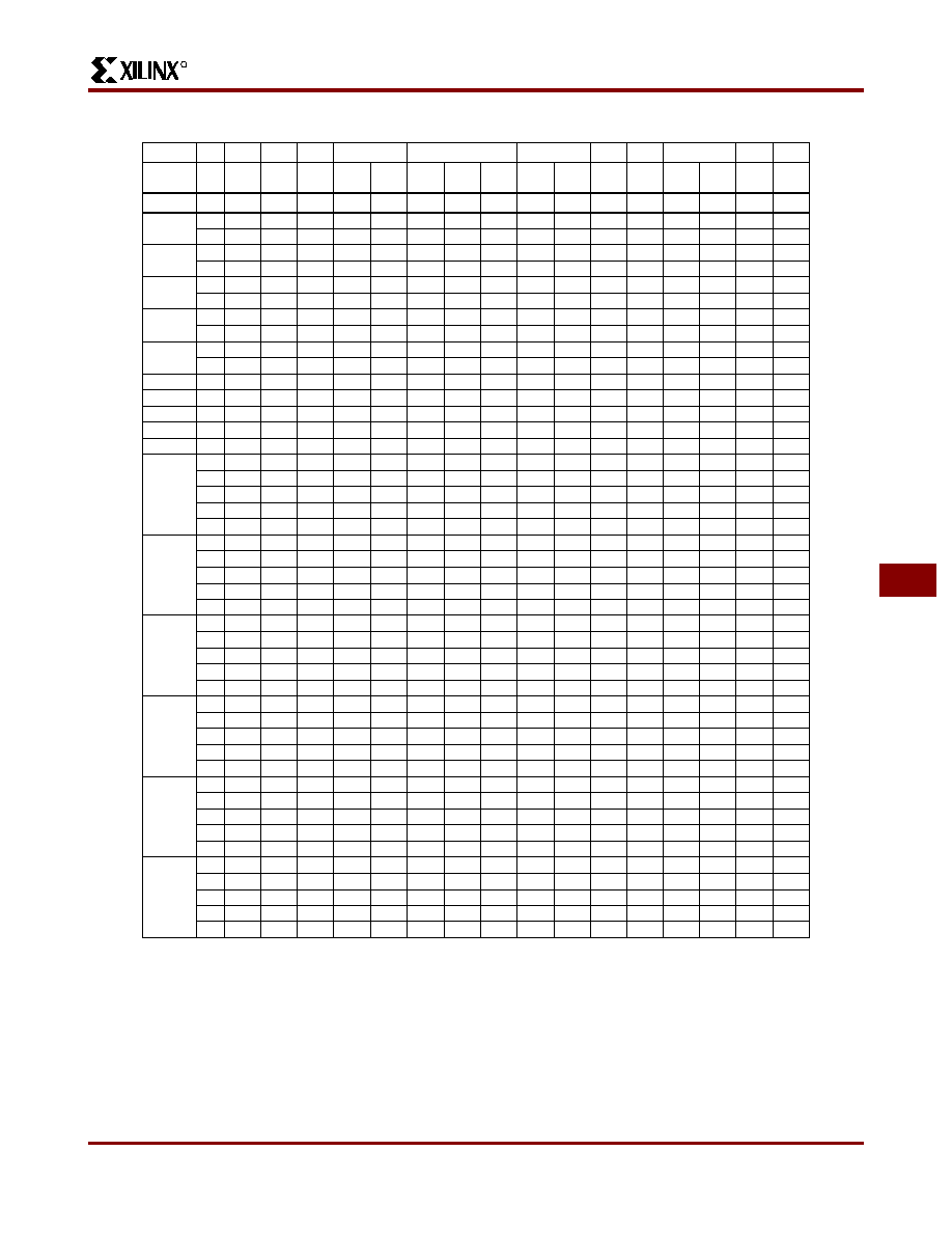
R
November 9, 1998 (Version 3.1)
7-77
XC3000 Series Field Programmable Gate Arrays
7
Product Availability
Pins
44
64
68
84
100
132
144
160
175
176
208
Type
Plast.
PLCC
Plast.
VQFP
Plast.
PLCC
Plast.
PLCC
Cer.
PGA
Plast.
PQFP
Plast.
TQFP
Plast.
VQFP
Plast.
PGA
Cer.
PGA
Plast.
TQFP
Plast.
PQFP
Plast.
PGA
Cer.
PGA
Plast.
TQFP
Plast.
PQFP
Code
PC44
VQ64
PC68
PC84
PG84
PQ100
TQ100
VQ100
PP132
PG132
TQ144
PQ160
PP175
PG175
TQ176
PQ208
XC3020A
-7
CI
CI
CI
-6
C
C
C
XC3030A
-7
CI
CI
CI
CI
CI
CI
-6
C
C
C
C
C
C
XC3042A
-7
CI
CI
CI
CI
CI
CI
-6
C
C
C
C
C
C
XC3064A
-7
CI
CI
CI
CI
CI
-6
C
C
C
C
C
XC3090A
-7
CI
CI
CI
CI
CI
CI
CI
-6
C
C
C
C
C
C
C
XC3020L
-8
CI
XC3030L
-8
CI
CI
CI
XC3042L
-8
CI
CI
CI
XC3064L
-8
CI
CI
XC3090L
-8
CI
CI
CI
XC3120A
-4
CI
CI
CI
-3
CI
CI
CI
-2
CI
CI
CI
-1
C
C
C
-09
C
C
C
XC3130A
-4
CI
CI
CI
CI
CI
CI
-3
CI
CI
CI
CI
CI
CI
-2
CI
CI
CI
CI
CI
CI
-1
C
C
C
C
C
C
-09
C
C
C
C
C
C
XC3142A
-4
CI
CI
C
CI
-3
CI
CI
CI
CI
-2
CI
CI
CI
CI
-1
C
C
C
C
-09
C
C
C
C
XC3164A
-4
CI
CI
CI
-3
CI
CI
CI
-2
CI
CI
CI
-1
C
C
C
-09
C
C
C
XC3190A
-4
CI
CI
CI
CI
CI
CI
CI
-3
CI
CI
CI
CI
CI
CI
CI
-2
CI
CI
CI
CI
CI
CI
CI
-1
C
C
C
C
C
C
C
-09
C
C
C
C
C
C
C
XC3195A
-4
CI
CI
CI
CI
CI
-3
CI
CI
CI
CI
CI
-2
CI
CI
CI
CI
CI
-1
C
C
C
C
C
-09
C
C
C
C
C
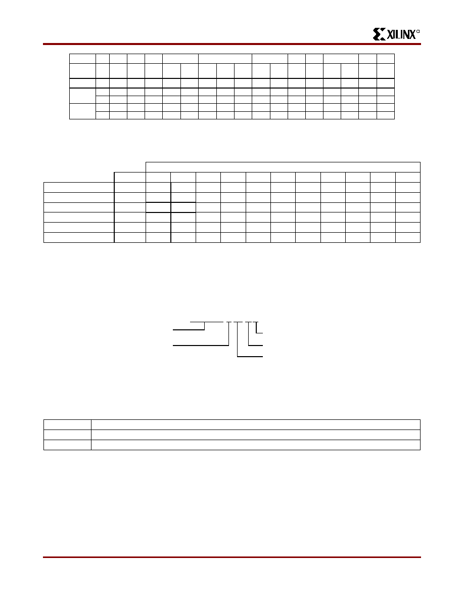
R
XC3000 Series Field Programmable Gate Arrays
7-78
November 9, 1998 (Version 3.1)
Number of Available I/O Pins
Ordering Information
Revision History
XC3142L
C
C
C
C
C
C
XC3190L
C
C
C
C
C
C
Notes:
C = Commercial, T
J
= 0
�
to +85
�
C
I = Industrial, T
J
= -40
�
to +100
�
C
Pins
44
64
68
84
100
132
144
160
175
176
208
Type
Plast.
PLCC
Plast.
VQFP
Plast.
PLCC
Plast.
PLCC
Cer.
PGA
Plast.
PQFP
Plast.
TQFP
Plast.
VQFP
Plast.
PGA
Cer.
PGA
Plast.
TQFP
Plast.
PQFP
Plast.
PGA
Cer.
PGA
Plast.
TQFP
Plast.
PQFP
Code
PC44
VQ64
PC68
PC84
PG84
PQ100
TQ100
VQ100
PP132
PG132
TQ144
PQ160
PP175
PG175
TQ176
PQ208
Number of Package Pins
Max I/O
44
64
68
84
100
132
144
160
175
176
208
XC3020A/XC3120A
64
58
64
64
XC3030A/XC3130A
80
34
54
58
74
80
XC3042A/3142A
96
74
82
96
96
XC2064A/XC3164A
120
70
110
120
120
XC3090A/XC3190A
144
70
122
138
144
144
144
XC3195A
176
70
138
144
176
XC3030A-3 PC44C
Example:
Device Type
Speed Grade
Temperature Range
Number of Pins
Package Type
Date
Revision
11/98
Revised version number to 3.1, removed XC3100A-5 obsolete packages.