
DS099 October 9, 2003
www.xilinx.com
Advance Product Specification
1-800-255-7778
� 2003 Xilinx, Inc. All rights reserved. All Xilinx trademarks, registered trademarks, patents, and disclaimers are as listed at
http://www.xilinx.com/legal.htm
.
All other trademarks and registered trademarks are the property of their respective owners. All specifications are subject to change without notice.
This document includes all four modules of the SpartanTM-3 FPGA data sheet.
Module 1:
Introduction and Ordering Information
DS099-1 (v1.1) April 24, 2003
6 pages
�
Introduction
�
Features
�
Architectural Overview
�
Product Availability
�
User I/O Chart
�
Ordering Information
Module 2:
Functional Description
DS099-2 (v1.2) July 11, 2003
40 pages
�
IOBs
-
IOB Overview
-
SelectIOTM Signal Standards
�
CLB Overview
�
Block RAM
�
Dedicated Multipliers
�
Digital Clock Manager (DCM)
-
Clock Network
�
Configuration
Module 3:
DC and Switching Characteristics
DS099-3 (v1.1) July 11, 2003
14 pages
�
DC Electrical Characteristics
-
Absolute Maximum Ratings
-
Recommended Operating Conditions
�
Configuration
-
Power-On Timing
-
Timing for the Configuration Modes
-
Timing for JTAG Port
�
Switching Characteristics
-
DLL Timing
Module 4:
Pinout Descriptions
DS099-4 (v1.2.2) October 9, 2003
98 pages
�
Pin Descriptions
-
Pin Behavior During Configuration
�
Package Overview
�
Pinout Tables
-
Footprints
IMPORTANT NOTE: The Spartan-3 1.2V FPGA data sheet is created and published in separate modules. This complete
version is provided for easy downloading and searching of the complete document. Page, figure, and table numbers begin
at 1 for each module, and each module has its own Revision History at the end. Use the PDF "Bookmarks" for easy
navigation in this volume.
0
Spartan-3 1.2V FPGA Family:
Complete Data Sheet
DS099 October 9, 2003
0
0
Advance Product Specification
R

DS099-1 (v1.1) April 24, 2003
www.xilinx.com
1
Advance Product Specification
1-800-255-7778
� 2003 Xilinx, Inc. All rights reserved. All Xilinx trademarks, registered trademarks, patents, and disclaimers are as listed at
http://www.xilinx.com/legal.htm
.
All other trademarks and registered trademarks are the property of their respective owners. All specifications are subject to change without notice.
Introduction
The 1.2V SpartanTM-3 family of Field-Programmable Gate
Arrays is specifically designed to meet the needs of high
volume, cost-sensitive consumer electronic applications.
The eight-member family offers densities ranging from
50,000 to five million system gates, as shown in
Table 1
.
The Spartan-3 family builds on the success of the earlier
Spartan-IIE family by increasing the amount of logic
resources, the capacity of internal RAM, the total number of
I/Os, and the overall level of performance as well as by
improving clock management functions. Numerous
enhancements derive from state-of-the-art VirtexTM-II tech-
nology. These Spartan-3 enhancements, combined with
advanced process technology, deliver more functionality
and bandwidth per dollar than was previously possible, set-
ting new standards in the programmable logic industry.
Because of their exceptionally low cost, Spartan-3 FPGAs
are ideally suited to a wide range of consumer electronics
applications, including broadband access, home network-
ing, display/projection and digital television equipment.
The Spartan-3 family is a superior alternative to mask pro-
grammed ASICs. FPGAs avoid the high initial cost, the
lengthy development cycles, and the inherent inflexibility of
conventional ASICs. Also, FPGA programmability permits
design upgrades in the field with no hardware replacement
necessary, an impossibility with ASICs.
Features
�
Revolutionary 90-nanometer process technology
�
Very low cost, high-performance logic solution for
high-volume, consumer-oriented applications
-
Densities as high as 74,880 logic cells
-
326 MHz system clock rate
-
Three separate power supplies for the core (1.2V),
I/Os (1.2V to 3.3V), and special functions (2.5V)
�
SelectIOTM signaling
-
Up to 784 I/O pins
-
622 Mb/s data transfer rate per I/O
-
Seventeen single-ended signal standards
-
Six differential signal standards including LVDS
-
Termination by Digitally Controlled Impedance
-
Signal swing ranging from 1.14V to 3.45V
-
Double Data Rate (DDR) support
�
Logic resources
-
Abundant, flexible logic cells with registers
-
Wide multiplexers
-
Fast look-ahead carry logic
-
Dedicated 18 x 18 multipliers
-
JTAG logic compatible with IEEE 1149.1/1532
standards
�
SelectRAMTM hierarchical memory
-
Up to 1,872 Kbits of total block RAM
-
Up to 520 Kbits of total distributed RAM
�
Digital Clock Manager (up to four DCMs)
-
Clock skew elimination
-
Frequency synthesis
-
High resolution phase shifting
�
Eight global clock lines and abundant routing
�
Fully supported by Xilinx ISE development system
-
Synthesis, mapping, placement and routing
06
Spartan-3 1.2V FPGA Family:
Introduction and Ordering
Information
DS099-1 (v1.1) April 24, 2003
0
0
Advance Product Specification
R
Table 1: Summary of Spartan-3 FPGA Attributes
Device
System
Gates
Logic
Cells
CLB Array
(One CLB = Four Slices)
Distributed
RAM (bits
1
)
Block RAM
(bits
1
)
Dedicated
Multipliers
DCMs
Maximum
User I/O
Maximum
Differential
I/O Pairs
Rows
Columns Total CLBs
XC3S50
50K
1,728
16
12
192
12K
72K
4
2
124
56
XC3S200
200K
4,320
24
20
480
30K
216K
12
4
173
76
XC3S400
400K
8,064
32
28
896
56K
288K
16
4
264
116
XC3S1000
1M
17,280
48
40
1,920
120K
432K
24
4
391
175
XC3S1500
1.5M
29,952
64
52
3,328
208K
576K
32
4
487
221
XC3S2000
2M
46,080
80
64
5,120
320K
720K
40
4
565
270
XC3S4000
4M
62,208
96
72
6,912
432K
1,728K
96
4
712
312
XC3S5000
5M
74,880
104
80
8,320
520K
1,872K
104
4
784
344
Notes:
1.
By convention, one Kb is equivalent to 1,024 bits.
Spartan-3 1.2V FPGA Family: Introduction and Ordering Information
2
www.xilinx.com
DS099-1 (v1.1) April 24, 2003
1-800-255-7778
Advance Product Specification
6
R
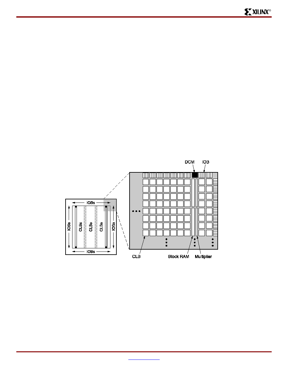
Architectural Overview
The Spartan-3 family architecture consists of five funda-
mental programmable functional elements:
�
Configurable Logic Blocks (CLBs) contain RAM-based
Look-Up Tables (LUTs) to implement logic and storage
elements that can be used as flip-flops or latches.
CLBs can be programmed to perform a wide variety of
logical functions as well as to store data.
�
Input/Output Blocks (IOBs) control the flow of data
between the I/O pins and the internal logic of the
device. Each IOB supports bidirectional data flow plus
3-state operation. Twenty-three different signal
standards, including six high-performance differential
standards, are available as shown in
Table 2
. Double
Data-Rate (DDR) registers are included. The Digitally
Controlled Impedance (DCI) feature provides
automatic on-chip terminations, simplifying board
designs.
�
Block RAM provides data storage in the form of 18-Kbit
dual-port blocks.
�
Multiplier blocks accept two 18-bit binary numbers as
inputs and calculate the product.
�
Digital Clock Manager (DCM) blocks provide
self-calibrating, fully digital solutions for distributing,
delaying, multiplying, dividing, and phase shifting clock
signals.
These elements are organized as shown in
Figure 1
. A ring
of IOBs surrounds a regular array of CLBs. The XC3S50
has a single column of block RAM embedded in the array.
Those devices ranging from the XC3S200 to the XC3S2000
have two columns of block RAM. The XC3S4000 and
XC3S5000 devices have four RAM columns. Each column
is made up of several 18K-bit RAM blocks; each block is
associated with a dedicated multiplier. The DCMs are posi-
tioned at the ends of each block RAM column.
The Spartan-3 family features a rich network of traces and
switches that interconnect all five functional elements,
transmitting signals among them. Each functional element
has an associated switch matrix that permits multiple con-
nections to the routing.
Figure 1: Spartan-3 Family Architecture
DS099-1_01_032703
Notes:
1.
The two additional block RAM columns of the XC3S4000 and XC3S5000
devices are shown with dashed lines. The XC3S50 has only the block RAM
column on the far left.

Spartan-3 1.2V FPGA Family: Introduction and Ordering Information
DS099-1 (v1.1) April 24, 2003
www.xilinx.com
3
Advance Product Specification
1-800-255-7778
R
Configuration
Spartan-3 FPGAs are programmed by loading configuration
data into robust static memory cells that collectively control
all functional elements and routing resources. Before pow-
ering on the FPGA, configuration data is stored externally in
a PROM or some other nonvolatile medium either on or off
the board. After applying power, the configuration data is
written to the FPGA using any of five different modes: Mas-
ter Parallel, Slave Parallel, Master Serial, Slave Serial and
Boundary Scan (JTAG). The Master and Slave Parallel
modes use an 8-bit wide SelectMAPTM Port.
The recommended memory for storing the configuration
data is the low-cost Xilinx Platform Flash PROM family,
which includes XCF00S PROMs for serial configuration and
XCF00P PROMs for parallel configuration.
I/O Capabilities
The SelectIO feature of Spartan-3 devices supports 17 sin-
gle-ended standards and six differential standards as listed
in
Table 2
.
Table 3
shows the number of user I/Os as well as
the number of differential I/O pairs available for each
device/package combination.
Table 2: Signal Standards Supported by the Spartan-3 Family
Standard
Category
Description
V
CCO
(V)
Class
Symbol
Single-Ended
GTL
Gunning Transceiver Logic
N/A
Terminated
GTL
Plus
GTLP
HSTL
High-Speed Transceiver Logic
1.5
I
HSTL_I
III
HSTL_III
1.8
I
HSTL_I_18
II
HSTL_II_18
III
HSTL_III_18
LVCMOS
Low-Voltage CMOS
1.2
N/A
LVCMOS12
1.5
N/A
LVCMOS15
1.8
N/A
LVCMOS18
2.5
N/A
LVCMOS25
3.3
N/A
LVCMOS33
LVTTL
Low-Voltage Transistor-Transistor Logic
3.3
N/A
LVTTL
PCI
Peripheral Component Interconnect
3.0
33 MHz
PCI33_3
SSTL
Stub Series Terminated Logic
1.8
N/A
SSTL18_I
2.5
I
SSTL2_I
II
SSTL2_II
Differential
LDT
Lightning Data Transport
(HyperTransportTM)
2.5
N/A
LDT_25
LVDS
Low Voltage Differential Signaling
Standard
LVDS_25
Bus
BLVDS_25
Extended Mode
LVDSEXT_25
Ultra
ULVDS_25
RSDS
Reduced-Swing Differential Signaling
2.5
N/A
RSDS_25

Spartan-3 1.2V FPGA Family: Introduction and Ordering Information
4
www.xilinx.com
DS099-1 (v1.1) April 24, 2003
1-800-255-7778
Advance Product Specification
6
R
Product Ordering and Availability
Table 4
shows all valid device ordering combinations of
device density, speed grade, package, and temperature
range parameters for the Spartan-3 family as well as the
availability status of those combinations.
Table 3: Spartan-3 User I/O Chart
Device
Available User I/Os and Differential (Diff) I/O Pairs
VQ100
TQ144
PQ208
FT256
FG456
FG676
FG900
FG1156
User
Diff
User
Diff
User
Diff
User
Diff
User
Diff
User
Diff
User
Diff
User
Diff
XC3S50
63
29
97
46
124
56
-
-
-
-
-
-
-
-
-
-
XC3S200
63
29
97
46
141
62
173
76
-
-
-
-
-
-
-
-
XC3S400
-
-
97
46
141
62
173
76
264
116
-
-
-
-
-
-
XC3S1000
-
-
-
-
-
-
173
76
333
149
391
175
-
-
-
-
XC3S1500
-
-
-
-
-
-
-
-
333
149
487
221
-
-
-
-
XC3S2000
-
-
-
-
-
-
-
-
-
-
489
221
565
270
-
-
XC3S4000
-
-
-
-
-
-
-
-
-
-
-
-
633
300
712
312
XC3S5000
-
-
-
-
-
-
-
-
-
-
-
-
633
300
784
344
Notes:
1.
All device options listed in a given package column are pin-compatible.
Table 4: Spartan-3 Device Availability
Package Type:
VQFP
TQFP
PQFP
FTBGA
FBGA
No. of Pins:
100
144
208
256
456
676
900
1156
Code:
VQ100
TQ144
PQ208
FT256
FG456
FG676
FG900
FG1156
Device
(1)
XC3S50
(C, I)
(C, I)
(C, I)
-
-
-
-
-
XC3S200
(C, I)
(C, I)
(C, I)
(C, I)
-
-
-
-
XC3S400
-
(C, I)
(C, I)
(C, I)
(C, I)
-
-
-
XC3S1000
-
-
-
(C, I)
(C, I)
(C, I)
-
-
XC3S1500
-
-
-
-
(C, I)
(C, I)
-
-
XC3S2000
-
-
-
-
-
(C, I)
(C, I)
-
XC3S4000
-
-
-
-
-
-
(C, I)
(C, I)
XC3S5000
-
-
-
-
-
-
(C, I)
(C, I)
Notes:
1.
Commercial devices are offered in the -4 and -5 speed grades; industrial devices are only in the -4 speed grade.
2.
C = Commercial, T
J
= 0
� to +85� C; I = Industrial, T
J
= �40
� C to +100� C.
3.
Parentheses indicate that a given device is not yet released to production. Contact your local sales office for availability information.
Spartan-3 1.2V FPGA Family: Introduction and Ordering Information
DS099-1 (v1.1) April 24, 2003
www.xilinx.com
5
Advance Product Specification
1-800-255-7778
R
Ordering Information
Revision History
The Spartan-3 Family Data Sheet
DS099-1, Spartan-3 1.2V FPGA Family: Introduction and Ordering Information (Module 1)
DS099-2, Spartan-3 1.2V FPGA Family:
Functional Description
(Module 2)
DS099-3, Spartan-3 1.2V FPGA Family:
DC and Switching Characteristics
(Module 3)
DS099-4, Spartan-3 1.2V FPGA Family:
Pinout Descriptions
(Module 4)
Date
Version No.
Description
04/11/03
1.0
Initial Xilinx release.
04/24/03
1.1
Updated block RAM, DCM, and multiplier counts for the XC3S50.
XC3S50 -4 PQ208 C
Example:
Temperature Range
Package Type / Number of Pins
Device Type
Speed Grade
Device
Speed Grade
Package Type / Number of Pins
Temperature Range (T
J
)
XC3S50
-4 Standard Performance
VQ100 100-pin Very Thin Quad Flat Pack (VQFP)
C Commercial (0�C to 85�C)
XC3S200
-5 High Performance
TQ144 144-pin Thin Quad Flat Pack (TQFP)
I
Industrial (�40�C to 100�C)
XC3S400
PQ208 208-pin Plastic Quad Flat Pack (PQFP)
XC3S1000
FT256 256-ball Fine-Pitch Thin Ball Grid Array (FTBGA)
XC3S1500
FG456 456-ball Fine-Pitch Ball Grid Array (FBGA)
XC3S2000
FG676 676-ball Fine-Pitch Ball Grid Array (FBGA)
XC3S4000
FG900 900-ball Fine-Pitch Ball Grid Array (FBGA)
XC3S5000
FG1156 1156-ball Fine-Pitch Ball Grid Array (FBGA)

Spartan-3 1.2V FPGA Family: Introduction and Ordering Information
6
www.xilinx.com
DS099-1 (v1.1) April 24, 2003
1-800-255-7778
Advance Product Specification
6
R
DS099-2 (v1.2) July 11, 2003
www.xilinx.com
1
Advance Product Specification
1-800-255-7778
� 2003 Xilinx, Inc. All rights reserved. All Xilinx trademarks, registered trademarks, patents, and disclaimers are as listed at
http://www.xilinx.com/legal.htm
.
All other trademarks and registered trademarks are the property of their respective owners. All specifications are subject to change without notice.
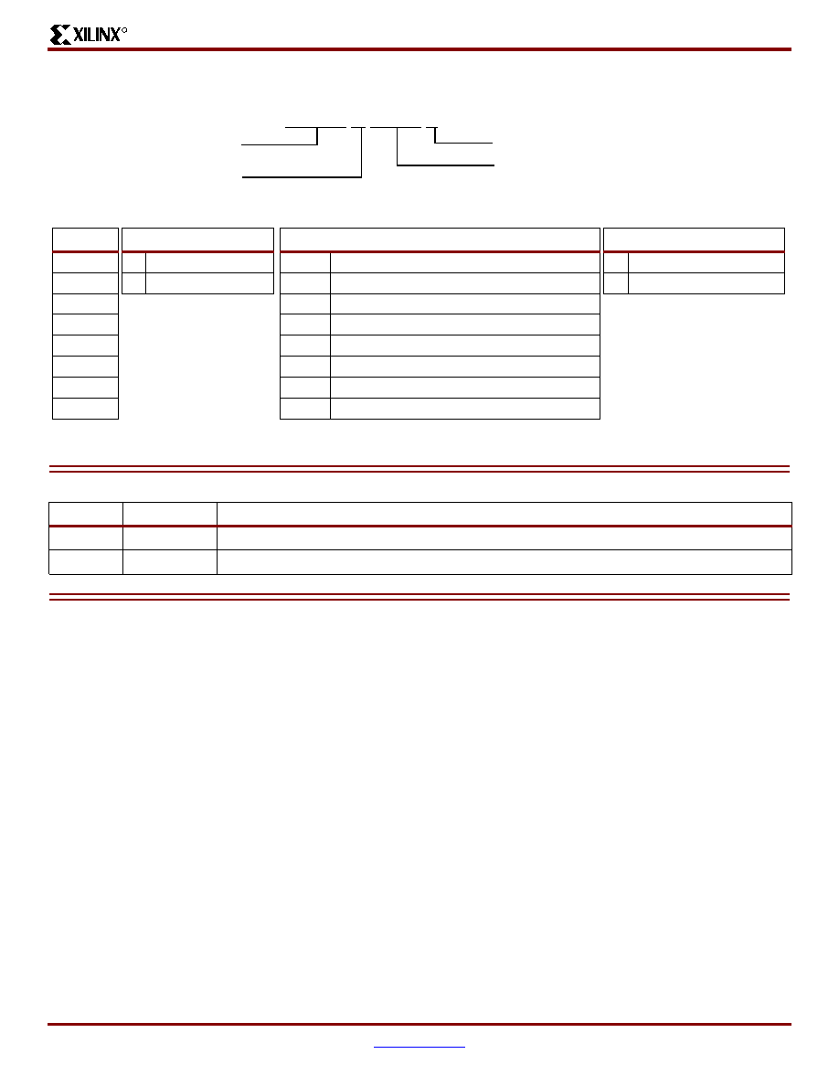
IOBs
IOB Overview
The Input/Output Block (IOB) provides a programmable,
bidirectional interface between an I/O pin and the FPGA's
internal logic.
A simplified diagram of the IOB's internal structure appears
in
Figure 1
. There are three main signal paths within the
IOB: the output path, input path, and 3-state path. Each
path has its own pair of storage elements that can act as
either registers or latches. For more information, see the
Storage Element Functions section. The three main signal
paths are as follows:
�
The input path carries data from the pad, which is
bonded to a package pin, through an optional
programmable delay element directly to the I line. After
the delay element, there are alternate routes through a
pair of storage elements to the IQ1 and IQ2 lines. The
IOB outputs I, IQ1, and IQ2 all lead to the FPGA's
internal logic. The delay element can be set to ensure a
hold time of zero.
�
The output path, starting with the O1 and O2 lines,
carries data from the FPGA's internal logic through a
multiplexer and then a three-state driver to the IOB
pad. In addition to this direct path, the multiplexer
provides the option to insert a pair of storage elements.
�
The 3-state path determines when the output driver is
high impedance. The T1 and T2 lines carry data from
the FPGA's internal logic through a multiplexer to the
output driver. In addition to this direct path, the
multiplexer provides the option to insert a pair of
storage elements.
�
All signal paths entering the IOB, including those
associated with the storage elements, have an inverter
option. Any inverter placed on these paths is
automatically absorbed into the IOB.
Storage Element Functions
There are three pairs of storage elements in each IOB, one
pair for each of the three paths. It is possible to configure
each of these storage elements as an edge-triggered
D-type flip-flop (FD) or a level-sensitive latch (LD).
The storage-element-pair on either the Output path or the
Three-State path can be used together with a special multi-
plexer to produce Double-Data-Rate (DDR) transmission.
This is accomplished by taking data synchronized to the
clock signal's rising edge and converting them to bits syn-
chronized on both the rising and the falling edge. The com-
bination of two registers and a multiplexer is referred to as a
Double-Data-Rate D-type flip-flop (FDDR).
See
Double-Data-Rate Transmission, page 3
for more
information.
The signal paths associated with the storage element are
described in
Table 1
.
040
Spartan-3 1.2V FPGA Family:
Functional Description
DS099-2 (v1.2) July 11, 2003
0
0
Advance Product Specification
R
Table 1: Storage Element Signal Description
Storage
Element
Signal
Description
Function
D
Data input
Data at this input is stored on the active edge of CK enabled by CE. For latch operation when the
input is enabled, data passes directly to the output Q.
Q
Data output
The data on this output reflects the state of the storage element. For operation as a latch in
transparent mode, Q will mirror the data at D.
CK
Clock input
A signal's active edge on this input with CE asserted, loads data into the storage element.
CE
Clock Enable input
When asserted, this input enables CK. If not connected, CE defaults to the asserted state.
SR
Set/Reset
Forces storage element into the state specified by the SRHIGH/SRLOW attributes. The
SYNC/ASYNC attribute setting determines if the SR input is synchronized to the clock or not.
REV
Reverse
Used together with SR. Forces storage element into the state opposite from what SR does.
Spartan-3 1.2V FPGA Family: Functional Description
2
www.xilinx.com
DS099-2 (v1.2) July 11, 2003
1-800-255-7778
Advance Product Specification
40
R
Figure 1: Simplified IOB Diagram
D
CE
CK
TFF1
Three-state Path
T
T1
TCE
T2
TFF2
Q
SR
DDR
MUX
REV
D
CE
CK
Q
SR
REV
D
CE
CK
OFF1
Output Path
O1
OCE
O2
OFF2
Q
SR
DDR
MUX
Weak
Keeper
Latch
V
CCO
V
REF
Pin
I/O Pin
from
Adjacent
IOB
DS099_01_040703
I/O
Pin
Program-
mable
Output
Driver
DCI
ESD
Weak
Pull-Up
Weak
Pull-
Down
ESD
REV
D
CE
CK
Q
SR
REV
OTCLK1
OTCLK2
D
CE
CK
IFF1
Input Path
I
ICE
IFF2
Q
SR
Fixed
Delay
LVCMOS, LVTTL, PCI
Single-ended Standards
using VREF
Differential Standards
REV
D
CE
CK
Q
SR
REV
ICLK1
ICLK2
SR
REV
Note: All IOB signals communicating with the FPGA's internal logic have the option of inverting polarity.
IQ1
IQ2

Spartan-3 1.2V FPGA Family: Functional Description
DS099-2 (v1.2) July 11, 2003
www.xilinx.com
3
Advance Product Specification
1-800-255-7778
R
According to
Figure 1
, the clock line OTCLK1 connects the
CK inputs of the upper registers on the output and
three-state paths. Similarly, OTCLK2 connects the CK
inputs for the lower registers on the output and three-state
paths. The upper and lower registers on the input path have
independent clock lines: ICLK1 and ICLK2.
The enable line OCE connects the CE inputs of the upper
and lower registers on the output path. Similarly, TCE con-
nects the CE inputs for the register pair on the three-state
path and ICE does the same for the register pair on the
input path.
The Set/Reset (SR) line entering the IOB is common to all
six registers, as is the Reverse (REV) line.
Each storage element supports numerous options in addi-
tion to the control over signal polarity described in the IOB
Overview section. These are described in
Table 2
.
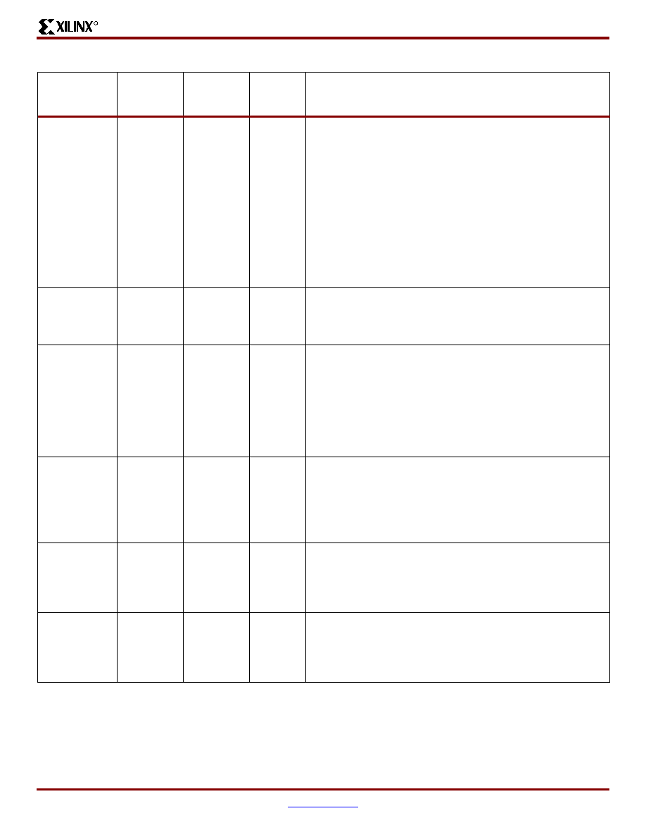
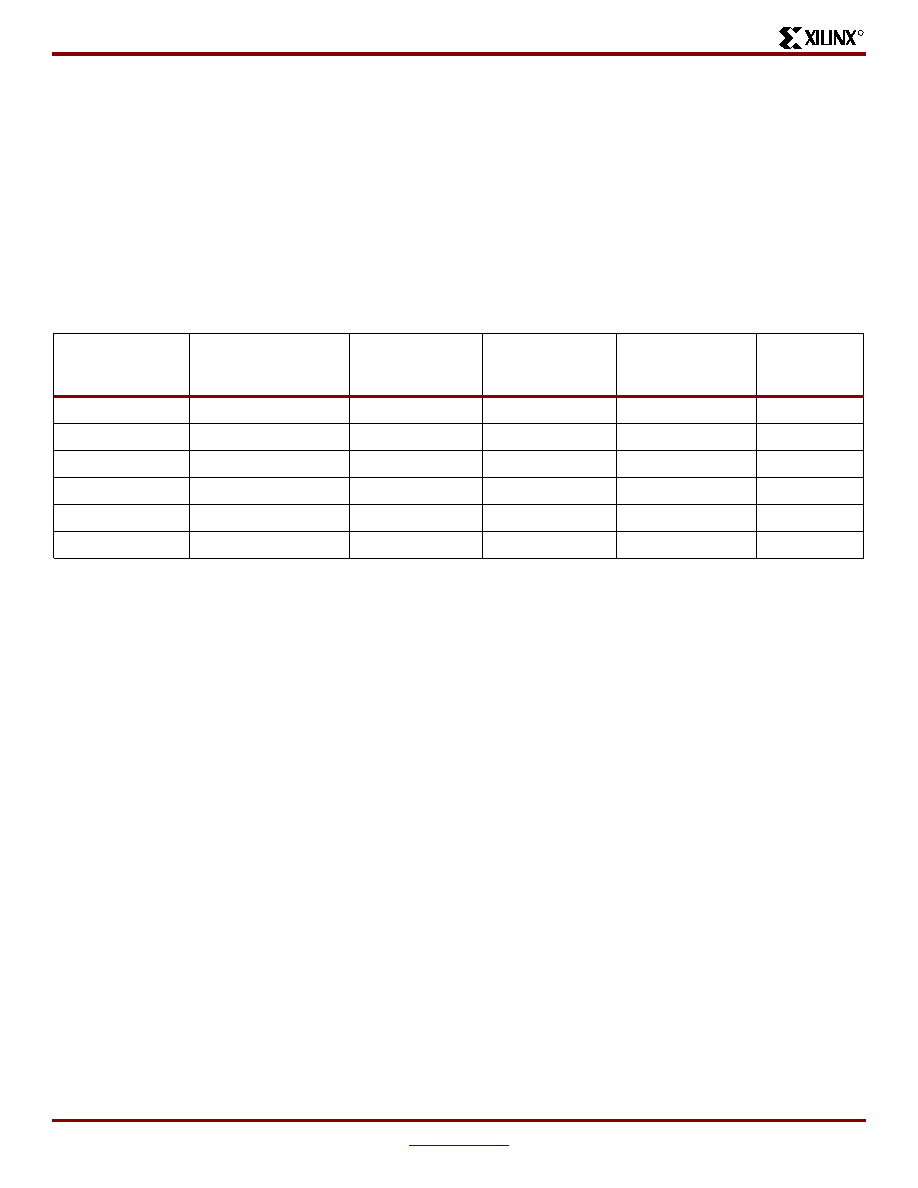
Double-Data-Rate Transmission
Double-Data-Rate (DDR) transmission describes the tech-
nique of synchronizing signals to both the rising and falling
edges of the clock signal. Spartan-3 devices use regis-
ter-pairs in all three IOB paths to perform DDR operations.
The pair of storage elements on the IOB's Output path
(OFF1 and OFF2), used as registers, combine with a spe-
cial multiplexer to form a DDR D-type flip-flop (FDDR). This
primitive permits DDR transmission where output data bits
are synchronized to both the rising and falling edges of a
clock. It is possible to access this function by placing either
an FDDRRSE or an FDDRCPE component or symbol into
the design. DDR operation requires two clock signals (50%
duty cycle), one the inverted form of the other. These sig-
nals trigger the two registers in alternating fashion, as
shown in
Figure 2
. Commonly, the Digital Clock Manager
(DCM) generates the two clock signals by mirroring an
incoming signal, then shifting it 180 degrees. This approach
ensures minimal skew between the two signals.
The storage-element-pair on the Three-State path (TFF1
and TFF2) can also be combined with a local multiplexer to
form an FDDR primitive. This permits synchronizing the out-
put enable to both the rising and falling edges of a clock.
This DDR operation is realized in the same way as for the
output path.
The storage-element-pair on the input path (IFF1 and IFF2)
allows an I/O to receive a DDR signal. An incoming DDR
clock signal triggers one register and the inverted clock sig-
nal triggers the other register. In this way, the registers take
turns capturing bits of the incoming DDR data signal.
Aside from high bandwidth data transfers, DDR can also be
used to reproduce, or "mirror", a clock signal on the output.
This approach is used to transmit clock and data signals
together. A similar approach is used to reproduce a clock
signal at multiple outputs. The advantage for both
approaches is that skew across the outputs will be minimal.
Table 2: Storage Element Options
Option Switch
Function
Specificity
FF/Latch
Chooses between an edge-sensitive flip-flop or
a level-sensitive latch
Independent for each storage element.
SYNC/ASYNC
Determines whether SR is synchronous or
asynchronous
Independent for each storage element.
SRHIGH/SRLOW
Determines whether SR acts as a Set, which
forces the storage element to a logic "1"
(SRHIGH) or a Reset, which forces a logic "0"
(SRLOW).
Independent for each storage element, except
when using FDDR. In the latter case, the selection
for the upper element (OFF1 or TFF2) will apply to
both elements.
INIT1/INIT0
In the event of a Global Set/Reset, after
configuration or upon activation of the GTS net,
this switch decides whether to set or reset a
storage element. By default, choosing SRLOW
also selects INIT0; choosing SRHIGH also
selects INIT1.
Independent for each storage element, except
when using FDDR. In the latter case, selecting
INIT0 for one element applies to both elements
(even though INIT1 is selected for the other).

Spartan-3 1.2V FPGA Family: Functional Description
4
www.xilinx.com
DS099-2 (v1.2) July 11, 2003
1-800-255-7778
Advance Product Specification
40
R
Pull-Up and Pull-Down Resistors
The optional pull-up and pull-down resistors are intended to
establish High and Low levels, respectively, at unused I/Os.
The weak pull-up resistor optionally connects each IOB pad
to V
CCO
. A weak pull-down resistor optionally connects
each pad to GND. These resistors are placed in a design
using the PULLUP and PULLDOWN symbols in a sche-
matic, respectively. They can also be instantiated as com-
ponents, set as constraints or passed as attributes in HDL
code. These resistors can also be selected for all unused
I/O using the Bitstream Generator (BitGen) option Unused-
Pin. A Low logic level on HSWAP_EN activates the pull-up
resistors on all I/Os during configuration.
Weak-Keeper Circuit
Each I/O has an optional weak-keeper circuit that retains
the last logic level on a line after all drivers have been turned
off. This is useful to keep bus lines from floating when all
connected drivers are in a high-impedance state. This func-
tion is placed in a design using the KEEPER symbol.
Pull-up and pull-down resistors override the weak-keeper
circuit.
ESD Protection
Clamp diodes protect all device pads against damage from
Electro-Static Discharge (ESD) as well as excessive voltage
transients. Each I/O has two clamp diodes: One diode
extends P-to-N from the pad to V
CCO
and a second diode
extends N-to-P from the pad to GND. During operation,
these diodes are normally biased in the off state. These
clamp diodes are always connected to the pad, regardless
of the signal standard selected. The presence of diodes lim-
its the ability of Spartan-3 I/Os to tolerate high signal volt-
ages. The V
IN
absolute maximum rating in
Table 1
in
Module 3:
DC and Switching Characteristics
specifies the
voltage range that I/Os can tolerate.
Slew Rate Control and Drive Strength
Two options, FAST and SLOW, control the output slew rate.
The FAST option supports output switching at a high rate.
The SLOW option reduces bus transients. These options are
only available when using one of the LVCMOS or LVTTL
standards, which also provide up to seven different levels of
current drive strength: 2, 4, 6, 8, 12, 16, and 24 mA. Choos-
ing the appropriate drive strength level is yet another means
to minimize bus transients.
Table 3
shows the drive strengths that the LVCMOS and
LVTTL standards support. The Fast option is indicated by
appending an "F" attribute after the output buffer symbol
OBUF or the bidirectional buffer symbol IOBUF. The Slow
option appends an "S" attribute. The drive strength in milliam-
peres follows the slew rate attribute. For example,
OBUF_LVCMOS18_S_6 or IOBUF_LVCMOS25_F_16.
Boundary-Scan Capability
All Spartan-3 IOBs support boundary-scan testing compat-
ible with IEEE 1149.1 standards. See
Boundary-Scan
(JTAG) Mode, page 36
for more information.
SelectIO
Signal Standards
The IOBs support 17 different single-ended signal stan-
dards, as listed in
Table 4
. Furthermore, the majority of
IOBs can be used in specific pairs supporting any of six dif-
ferential signal standards, as shown in
Table 5
. The desired
standard is selected by placing the appropriate I/O library
symbol or component into the FPGA design. For example,
the symbol named IOBUF_LVCMOS15_F_8 represents a
bidirectional I/O to which the 1.5V LVCMOS signal standard
has been assigned. The slew rate and current drive are set
to Fast and 8 mA, respectively.
Together with placing the appropriate I/O symbol, two exter-
nally applied voltage levels, V
CCO
and V
REF
select the
desired signal standard. The V
CCO
lines provide current to
the output driver. The voltage on these lines determines the
Figure 2: Clocking the DDR Register
D1
CLK1
DDR MUX
DCM
Q1
FDDR
D2
CLK2
Q2
180� 0�
DS099-2_02_070303
Q
Table 3: Programmable Output Drive Current
Signal
Standard
Current Drive (mA)
2
4
6
8
12
16
24
LVCMOS12
-
-
-
-
LVCMOS15
-
-
LVCMOS18
-
LVCMOS25
LVCMOS33
LVTTL
Spartan-3 1.2V FPGA Family: Functional Description
DS099-2 (v1.2) July 11, 2003
www.xilinx.com
5
Advance Product Specification
1-800-255-7778
R
output voltage swing for all standards except GTL and
GTLP.
All single-ended standards except the LVCMOS modes
require a Reference Voltage (V
REF
) to bias the input-switch-
ing threshold. Once a configuration data file is loaded into
the FPGA that calls for the I/Os of a given bank to use such
a signal standard, a few specifically reserved I/O pins on the
same bank automatically convert to V
REF
inputs. When
using one of the LVCMOS standards, these pins remain
I/Os because the V
CCO
voltage biases the input-switching
threshold, so there is no need for V
REF
. Select the V
CCO
and
V
REF
levels to suit the desired single-ended standard
according to
Table 4
.
Differential standards employ a pair of signals, one the
opposite polarity of the other. The noise canceling (e.g.,
Common-Mode Rejection) properties of these standards
permit exceptionally high data transfer rates. This section
introduces the differential signaling capabilities of Spartan-3
devices.
Each device-package combination designates specific I/O
pairs that are specially optimized to support differential
standards. A unique "L-number", part of the pin name, iden-
tifies the line-pairs associated with each bank (see Module
4:
Pinout Descriptions
). For each pair, the letters "P" and
"N" designate the true and inverted lines, respectively. For
example, the pin names IO_L43P_7 and IO_L43N_7 indi-
cate the true and inverted lines comprising the line pair L43
on Bank 7. The differential Output Voltage (V
OD
) parameter
measures the voltage difference the High and Low logic lev-
els that a pair of differential outputs drive. The V
OD
range for
each of the differential standards is listed in
Table 5
. The
V
CCO
lines provide current to the outputs. The V
REF
lines
are not used. Select the V
CCO
level to suit the desired differ-
ential standard according to
Table 5
.
The need to supply V
REF
and V
CCO
imposes constraints on
which standards can be used in the same bank. See
The
Organization of IOBs into Banks
section for additional
guidelines concerning the use of the V
CCO
and V
REF
lines.
Digitally Controlled Impedance (DCI)
When the round-trip delay of an output signal -- i.e., from
output to input and back again -- exceeds rise and fall
times, it is common practice to add termination resistors to
the line carrying the signal. These resistors effectively
match the impedance of a device's I/O to the characteristic
impedance of the transmission line, thereby preventing
reflections that adversely affect signal integrity. However,
with the high I/O counts supported by modern devices, add-
ing resistors requires significantly more components and
board area. Furthermore, for some packages -- e.g., ball
grid arrays -- it may not always be possible to place resis-
tors close to pins.
DCI answers these concerns by providing two kinds of
on-chip terminations: Parallel terminations make use of an
integrated resistor network. Series terminations result from
controlling the impedance of output drivers. DCI actively
adjusts both parallel and series terminations to accurately
Table 4: Single-Ended I/O Standards (Values in Volts)
Signal
Standard
V
CCO
V
REF
for
Inputs
(1)
Board
Termination
Voltage (V
TT
)
For
Outputs
For
Inputs
GTL
Note 2
Note 2
0.8
1.2
GTLP
Note 2
Note 2
1
1.5
HSTL_I
1.5
-
0.75
0.75
HSTL_III
1.5
-
0.9
1.5
HSTL_I_18
1.8
-
0.9
0.9
HSTL_II_18
1.8
-
0.9
0.9
HSTL_III_18
1.8
-
1.1
1.8
LVCMOS12
1.2
1.2
-
-
LVCMOS15
1.5
1.5
-
-
LVCMOS18
1.8
1.8
-
-
LVCMOS25
2.5
2.5
-
-
LVCMOS33
3.3
3.3
-
-
LVTTL
3.3
3.3
-
-
PCI33_3
3.0
3.0
-
-
SSTL18_I
1.8
-
0.9
0.9
SSTL2_I
2.5
-
1.25
1.25
SSTL2_II
2.5
-
1.25
1.25
Notes:
1.
Banks 4 and 5 of any Spartan-3 device in a VQ100 package
do not support signal standards using V
REF
.
2.
The V
CCO
level used for the GTL and GTLP standards must
be no lower than the termination voltage (V
TT
), nor can it be
lower than the voltage at the I/O pad.
3.
See
Table 6
for a listing of the single-ended DCI standards.
Table 5: Differential I/O Standards
Signal
Standard
V
CCO
(Volts)
V
REF
for
Inputs
(Volts)
V
OD
(1)
(mV)
For
Outputs
For
Inputs
Min.
Max.
LDT_25
2.5
-
-
430
670
LVDS_25
2.5
-
-
250
400
BLVDS_25
2.5
-
-
250
450
LVDSEXT_25
2.5
-
-
330
700
ULVDS_25
2.5
-
-
430
670
RSDS_25
2.5
-
-
100
400
Notes:
1.
Measured with a termination resistor value (RT) of 100
Ohms.
2.
See
Table 6
for a listing of the differential DCI standards.
Table 4: Single-Ended I/O Standards (Values in Volts)
Signal
Standard
V
CCO
V
REF
for
Inputs
(1)
Board
Termination
Voltage (V
TT
)
For
Outputs
For
Inputs

Spartan-3 1.2V FPGA Family: Functional Description
6
www.xilinx.com
DS099-2 (v1.2) July 11, 2003
1-800-255-7778
Advance Product Specification
40
R
match the characteristic impedance of the transmission line.
This adjustment process compensates for differences in I/O
impedance that can result from normal variation in the
ambient temperature, the supply voltage and the manufac-
turing process. When the output driver turns off, the series
termination, by definition, approaches a very high imped-
ance; in contrast, parallel termination resistors remain at the
targeted values.
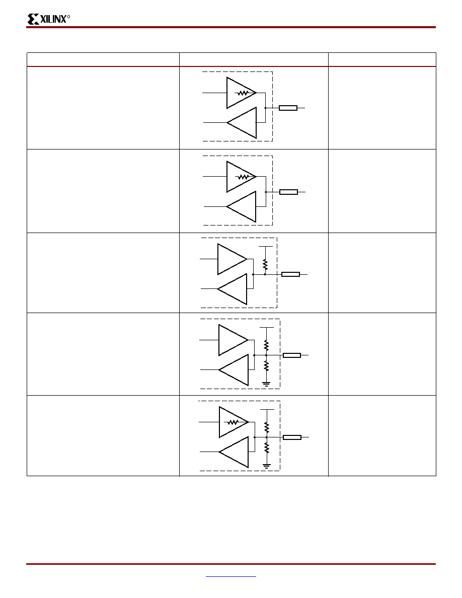
DCI is available only for certain I/O standards, as listed in
Table 6
. DCI is selected by applying the appropriate I/O
standard extensions to symbols or components. There are
five basic ways to configure terminations, as shown in
Table 7
. The DCI I/O standard determines which of these
terminations is put into effect.
Table 6: DCI I/O Standards
Category of Signal
Standard
Signal Standard
V
CCO
(V)
V
REF
for
Inputs (V)
Termination Type
For
Outputs
For
Inputs
At Output
At Input
Single-Ended
Gunning
Transceiver Logic
GTL_DCI
1.2
1.2
0.8
Single
Single
GTLP_DCI
1.5
1.5
1.0
High-Speed
Transceiver Logic
HSTL_I_DCI
1.5
1.5
0.75
None
Split
HSTL_III_DCI
1.5
1.5
0.9
None
Single
HSTL_I_DCI_18
1.8
1.8
0.9
None
Split
HSTL_II_DCI_18
1.8
1.8
0.9
Split
HSTL_III_DCI_18
1.8
1.8
1.1
None
Single
Low-Voltage CMOS
LVDCI_15
1.5
1.5
-
Controlled impedance
driver
None
LVDCI_18
1.8
1.8
-
LVDCI_25
2.5
2.5
-
LVDCI_33
3.3
3.3
-
LVDCI_DV2_15
1.5
1.5
-
Controlled driver with
half-impedance
LVDCI_DV2_18
1.8
1.8
-
LVDCI_DV2_25
2.5
2.5
-
LVDCI_DV2_33
3.3
3.3
-
Stub Series
Terminated Logic
SSTL18_I_DCI
1.8
1.8
0.9
25-Ohm driver
Split
SSTL2_I_DCI
2.5
2.5
1.25
25-Ohm driver
SSTL2_II_DCI
2.5
2.5
1.25
Split with 25-Ohm driver
Differential
Low-Voltage
Differential
Signalling
LVDS_25_DCI
2.5
2.5
-
None
Split on
each line
of pair
LVDSEXT_25_DCI
2.5
2.5
-
Notes:
1.
Bank 5 of any Spartan-3 device in a VQ100 or TQ144 package does not support DCI signal standards.
Spartan-3 1.2V FPGA Family: Functional Description
DS099-2 (v1.2) July 11, 2003
www.xilinx.com
7
Advance Product Specification
1-800-255-7778
R
Table 7: DCI Terminations
Termination
Schematic
(1)
I/O Standards
Controlled impedance output driver
LVDCI_15
LVDCI_18
LVDCI_25
LVDCI_33
Controlled output driver with half impedance
LVDCI_DV2_15
LVDCI_DV2_18
LVDCI_DV2_25
LVDCI_DV2_33
Single resistor
GTL_DCI
GTLP_DCI
HSTL_III_DCI
(2)
HSTL_III_DCI_18
(2)
Split resistors
HSTL_I_DCI
(2)
HSTL_I_DCI_18
(2)
HSTL_II_DCI_18
LVDS_25_DCI
LVDSEXT_25_DCI
Split resistors with output driver impedance
fixed to 25
SSTL18_I_DCI
(3)
SSTL2_I_DCI
(3)
SSTL2_II_DCI
Notes:
1.
The value of R is equivalent to the characteristic impedance of the line connected to the I/O. It is also equal to half the value of R
REF
for the DV2 standards and R
REF
for all other DCI standards.
2.
For DCI using HSTL Classes I and III, terminations only go into effect at inputs (not at outputs).
3.
For DCI using SSTL Class I, the split termination only goes into effect at inputs (not at outputs).
Z
0
IOB
R
Z
0
IOB
R/2
R
Z
0
V
CCO
IOB
2R
2R
Z
0
V
CCO
IOB
25
2R
2R
Z
0
V
CCO
IOB

Spartan-3 1.2V FPGA Family: Functional Description
8
www.xilinx.com
DS099-2 (v1.2) July 11, 2003
1-800-255-7778
Advance Product Specification
40
R
The DCI feature operates independently for each of the
device's eight banks. Each bank has an "N" reference pin
(VRN) and a "P" reference pin, (VRP), to calibrate driver
and termination resistance. Only when using a DCI stan-
dard on a given bank do these two pins function as VRN
and VRP. When not using a DCI standard, the two pins func-
tion as user I/Os. As shown in
Figure 3
, add an external ref-
erence resistor to pull the VRN pin up to V
CCO
and
another
reference resistor to pull the VRP pin down to GND. Both
resistors have the same value -- commonly 50 Ohms --
with one-percent tolerance, which is either the characteristic
impedance of the line or twice that, depending on the DCI
standard in use. Standards having a symbol name that con-
tains the letters "DV2" use a reference resistor value that is
twice the line impedance. DCI adjusts the output driver
impedance to match the reference resistors' value or half
that, according to the standard. DCI always adjusts the
on-chip termination resistors to directly match the reference
resistors' value.
The rules guiding the use of DCI standards on banks are as
follows:
1.
No more than one DCI I/O standard with a Single
Termination is allowed per bank.
2.
No more than one DCI I/O standard with a Split
Termination is allowed per bank.
3.
Single Termination, Split Termination, Controlled-
Impedance Driver, and Controlled-Impedance Driver
with Half Impedance can co-exist in the same bank.
See also
The Organization of IOBs into Banks, page 8
.
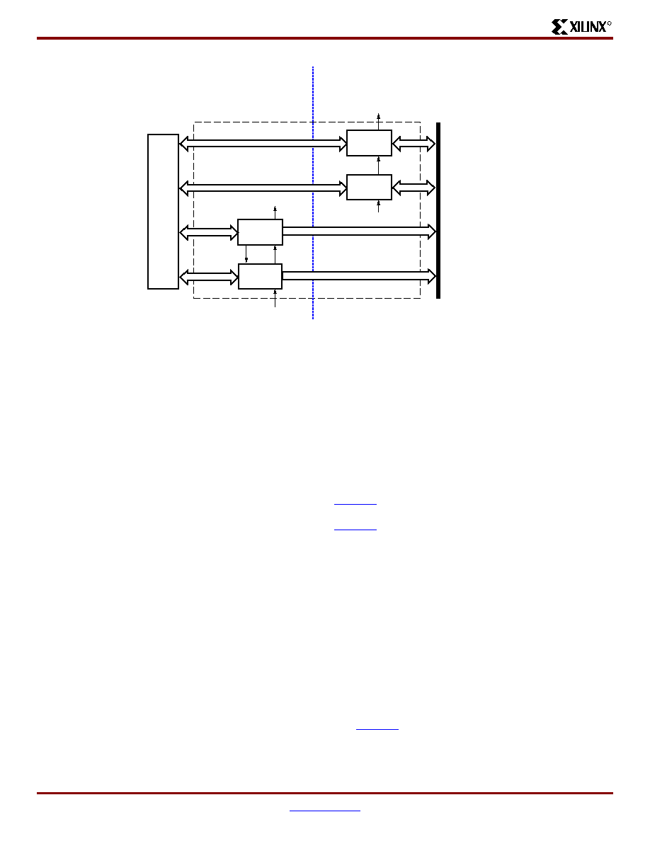
The Organization of IOBs into Banks
IOBs are allocated among eight banks, so that each side of
the device has two banks, as shown in
Figure 4
. For all
packages, each bank has independent V
REF
lines. For
example, V
REF
Bank 3 lines are separate from the V
REF
lines going to all other banks.
For the Very Thin Quad Flat Pack (VQ), Plastic Quad Flat
Pack (PQ), Fine Pitch Thin Ball Grid Array (FT), and Fine
Pitch Ball Grid Array (FG) packages, each bank has dedi-
cated V
CCO
lines. For example, the V
CCO
Bank 7 lines are
separate from the V
CCO
lines going to all other banks. Thus,
Spartan-3 devices in these packages support eight inde-
pendent V
CCO
supplies.
In contrast, the 144-pin Thin Quad Flat Pack (TQ144) pack-
age ties V
CCO
together internally for the pair of banks on
each side of the device. For example, the V
CCO
Bank 0 and
the V
CCO
Bank 1 lines are tied together. The interconnected
bank-pairs are 0/1, 2/3, 4/5, and 6/7. As a result, Spartan-3
devices in the TQ144 package support four independent
V
CCO
supplies.
Spartan-3 Compatibility
Within the Spartan-3 family, all devices are pin-compatible
by package. When the need for future logic resources out-
grows the capacity of the Spartan-3 device in current use, a
larger device in the same package can serve as a direct
replacement. Larger devices may add extra V
REF
and V
CCO
lines to support a greater number of I/Os. In the larger
device, more pins can convert from user I/Os to V
REF
lines.
Also, additional V
CCO
lines are bonded out to pins that were
"not connected" in the smaller device. Thus, it is important
to plan for future upgrades at the time of the board's initial
design by laying out connections to the extra pins.
The Spartan-3 family is not pin-compatible with any previ-
ous Xilinx FPGA family.
Rules Concerning Banks
When assigning I/Os to banks, it is important to follow the
following V
CCO
rules:
1.
Leave no V
CCO
pins unconnected on the FPGA.
2.
Set all V
CCO
lines associated with the (interconnected)
bank to the same voltage level.
3.
The V
CCO
levels used by all standards assigned to the
I/Os of the (interconnected) bank(s) must agree. The
Xilinx development software checks for this. Tables
4
,
5
,
and
6
describe how different standards use the V
CCO
supply.
Figure 3: Connection of Reference Resistors (R
REF
)
DS099-2_04_091602
VCCO
VRN
VRP
One of eight
I/O Banks
R
REF
(1%)
R
REF
(1%)
Figure 4: Spartan-3 I/O Banks (top view)
DS099-2_03_060102
Bank 0
Bank 1
Bank 5
Bank 4
Bank 7
Bank 6
Bank 2
Bank 3

Spartan-3 1.2V FPGA Family: Functional Description
DS099-2 (v1.2) July 11, 2003
www.xilinx.com
9
Advance Product Specification
1-800-255-7778
R
4.
If none of the standards assigned to the I/Os of the
(interconnected) bank(s) use V
CCO
, tie all associated
V
CCO
lines to 2.5V.
5.
In general, apply 2.5V to V
CCO
Bank 4 from power-on to
the end of configuration. Apply the same voltage to
V
CCO
Bank 5 during parallel configuration or a
Readback operation. For information on how to
program the FPGA using 3.3V signals and power, see
the
3.3V-Tolerant Configuration Interface
section.
If any of the standards assigned to the Inputs of the bank
use V
REF
, then observe the following additional rules:
1.
Leave no V
REF
pins unconnected on any bank.
2.
Set all V
REF
lines associated with the bank to the same
voltage level.
3.
The V
REF
levels used by all standards assigned to the
Inputs of the bank must agree. The Xilinx development
software checks for this. Tables
4
and
6
describe how
different standards use the V
REF
supply.
If none of the standards assigned to the Inputs of a bank
use V
REF
for biasing input switching thresholds, all associ-
ated V
REF
pins function as User I/Os.
Exceptions to Banks Supporting I/O
Standards
Bank 5 of any Spartan-3 device in a VQ100 or TQ144 pack-
age does not support DCI signal standards. In this case,
bank 5 has neither VRN nor VRP pins.
Furthermore, banks 4 and 5 of any Spartan-3 device in a
VQ100 package do not support signal standards using
V
REF
(see
Table 4
). In this case, the two banks do not have
any V
REF
pins.
Supply Voltages for the IOBs
Three different supplies power the IOBs:
1.
The V
CCO
supplies, one for each of the FPGA's I/O
banks, power the output drivers, except when using the
GTL and GTLP signal standards. The voltage on the
V
CCO
pins determines the voltage swing of the output
signal.
2.
V
CCINT
is the main power supply for the FPGA's internal
logic.
3.
The V
CCAUX
is an auxiliary source of power, primarily to
optimize the performance of various FPGA functions
such as I/O switching.
The I/Os During Power-On, Configuration, and
User Mode
With no power applied to the FPGA, all I/Os are in a
high-impedance state. The V
CCINT
(1.2V), V
CCAUX
(2.5V),
and V
CCO
supplies may be applied in any order. Before
power-on can finish, V
CCINT
, V
CCO
Bank 4, and V
CCAUX
must have reached their respective minimum recom-
mended operating levels (see
Table 2
in Module 3:
DC and
Switching Characteristics
). At this time, all I/O drivers
also will be in a high-impedance state. V
CCO
Bank 4,
V
CCINT
, and V
CCAUX
serve as inputs to the internal
Power-On Reset circuit (POR).
A Low level applied to HSWAP_EN input enables weak
pull-up resistors on User I/Os from power-on throughout
configuration. A High level on HSWAP_EN disables the
pull-up resistors, allowing the I/Os to float. As soon as
power is applied, the FPGA begins initializing its configura-
tion memory. At the same time, the FPGA internally asserts
the Global Set-Reset (GSR), which asynchronously resets
all IOB storage elements to a Low state.
Upon the completion of initialization, INIT_B goes High,
sampling the M0, M1, and M2 inputs to determine the con-
figuration mode. At this point, the configuration data is
loaded into the FPGA. The I/O drivers remain in a
high-impedance state (with or without pull-up resistors, as
determined by the HSWAP_EN input) throughout configura-
tion.
The Global Three State (GTS) net is released during
Start-Up, marking the end of configuration and the begin-
ning of design operation in the User mode. At this point,
those I/Os to which signals have been assigned go active
while all unused I/Os remain in a high-impedance state. The
release of the GSR net, also part of Start-up, leaves the IOB
registers in a Low state by default, unless the loaded design
reverses the polarity of their respective RS inputs.
In User mode, all weak, internal pull-up resistors on the I/Os
are disabled and HSWAP_EN becomes a "don't care" input.
If it is desirable to have weak pull-up or pull-down resistors
on I/Os carrying signals, the appropriate symbol -- e.g.,
PULLUP, PULLDOWN -- must be placed at the appropriate
pads in the design. The Bitstream Generator (Bitgen) option
UnusedPin available in the Xilinx development software
determines whether unused I/Os collectively have pull-up
resistors, pull-down resistors, or no resistors in User mode.
Spartan-3 1.2V FPGA Family: Functional Description
10
www.xilinx.com
DS099-2 (v1.2) July 11, 2003
1-800-255-7778
Advance Product Specification
40
R
.
CLB Overview
The Configurable Logic Blocks (CLBs) constitute the main
logic resource for implementing synchronous as well as
combinatorial circuits. Each CLB comprises four intercon-
nected slices, as shown in
Figure 5
. These slices are
grouped in pairs. Each pair is organized as a column with an
independent carry chain.
The nomenclature that the FPGA Editor -- part of the Xilinx
development software -- uses to designate slices is as fol-
lows: The letter "X" followed by a number identifies columns
of slices. The "X" number counts up in sequence from the
left side of the die to the right. The letter "Y" followed by a
number identifies the position of each slice in a pair as well
as indicating the CLB row. The "Y" number counts slices
starting from the bottom of the die according to the
sequence: 0, 1, 0, 1 (the first CLB row); 2, 3, 2, 3 (the sec-
ond CLB row); etc.
Figure 5
shows the CLB located in the
lower left-hand corner of the die. Slices X0Y0 and X0Y1
make up the column-pair on the left where as slices X1Y0
and X1Y1 make up the column-pair on the right. For each
CLB, the term "left-hand" (or SLICEM) is used to indicated
the pair of slices labeled with an even "X" number, such as
X0, and the term "right-hand" (or SLICEL) designates the
pair of slices with an odd "X" number, e.g., X1.
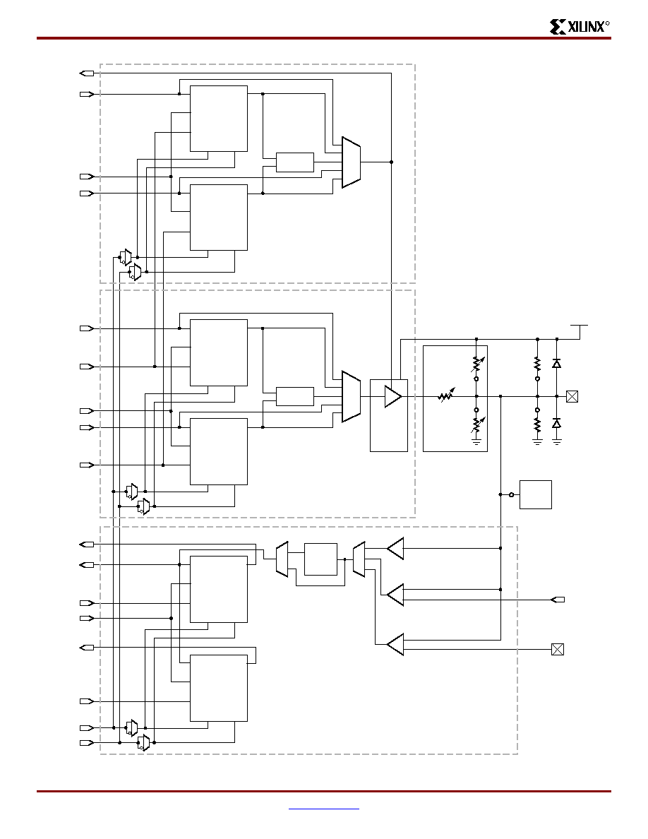
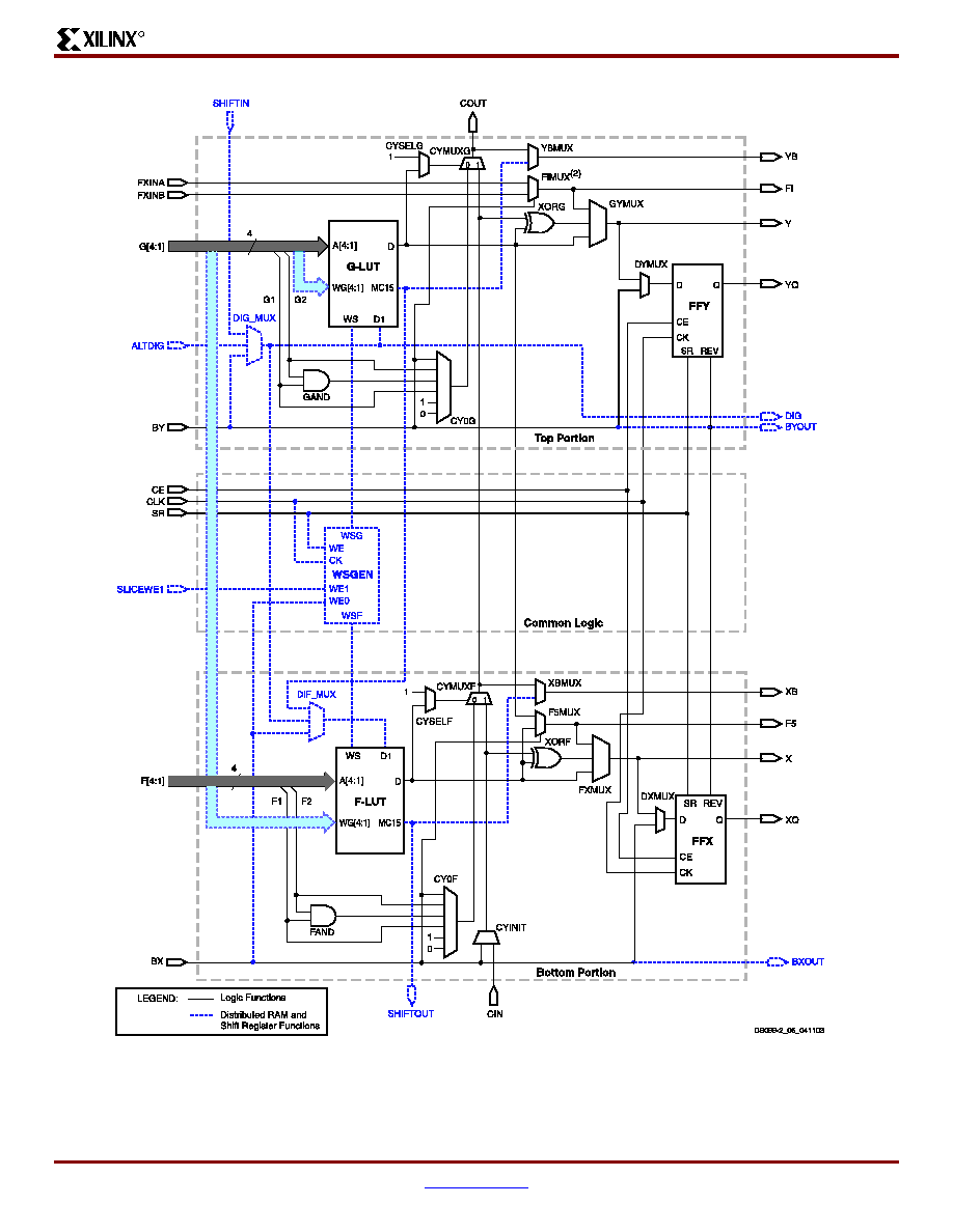
Elements Within a Slice
All four slices have the following elements in common: two
logic function generators, two storage elements, wide-func-
tion multiplexers, carry logic, and arithmetic gates, as
shown in
Figure 6
. Both the left-hand and right-hand slice
pairs use these elements to provide logic, arithmetic, and
ROM functions. Besides these, the left-hand pair supports
two additional functions: storing data using Distributed RAM
and shifting data with 16-bit registers.
Figure 6
is a diagram
of the left-hand slice; therefore, it represents a superset of
the elements and connections to be found in all slices. See
Function Generator, page 12
for more information.
The RAM-based function generator -- also known as a
Look-Up Table or LUT -- is the main resource for imple-
menting logic functions. Furthermore, the LUTs in each
left-hand slice pair can be configured as Distributed RAM or
a 16-bit shift register. For information on the former, see
XAPP464
: Using Look-Up Tables as Distributed RAM in
Spartan-3 FPGAs; for information on the latter, refer to
XAPP465
: Using Look-Up Tables as Shift Registers (SRL16)
in Spartan-3 FPGAs. The function generators located in the
upper and lower portions of the slice are referred to as the
"G" and "F", respectively.
The storage element, which is programmable as either a
D-type flip-flop or a level-sensitive latch, provides a means
for synchronizing data to a clock signal, among other uses.
The storage elements in the upper and lower portions of the
slice are called FFY and FFX, respectively.
Wide-function multiplexers effectively combine LUTs in
order to permit more complex logic operations. Each slice
has two of these multiplexers with F5MUX in the lower por-
tion of the slice and FXMUX in the upper portion. Depend-
ing on the slice, FXMUX takes on the name F6MUX,
F7MUX, or F8MUX. For more details on the multiplexers,
see
XAPP466
: Using Dedicated Multiplexers in Spartan-3
FPGAs.
Figure 5: Arrangement of Slices within the CLB
DS099-2_05_040703
Interconnect
to Neighbors
Left-Hand SLICEM
(Logic or Distributed RAM
or Shift Register)
Right-Hand SLICEL
(Logic Only)
CIN
SLICE
X0Y1
SLICE
X0Y0
Switch
Matrix
COUT
CLB
COUT
SHIFTOUT
SHIFTIN
CIN
SLICE
X1Y1
SLICE
X1Y0
Spartan-3 1.2V FPGA Family: Functional Description
DS099-2 (v1.2) July 11, 2003
www.xilinx.com
11
Advance Product Specification
1-800-255-7778
R
Figure 6: Simplified Diagram of the Left-Hand SLICEM
Notes:
1.
Options to invert signal polarity as well as other options that enable lines for various functions are not shown.
2.
The index i can be 6, 7, or 8, depending on the slice. In this position, the upper right-hand slice has an F8MUX,
and the upper left-hand slice has an F7MUX. The lower right-hand and left-hand slices both have an F6MUX.

Spartan-3 1.2V FPGA Family: Functional Description
12
www.xilinx.com
DS099-2 (v1.2) July 11, 2003
1-800-255-7778
Advance Product Specification
40
R
The carry chain, together with various dedicated arithmetic
logic gates, support fast and efficient implementations of
math operations. The carry chain enters the slice as CIN
and exits as COUT. Five multiplexers control the chain:
CYINIT, CY0F, and CYMUXF in the lower portion as well as
CY0G and CYMUXG in the upper portion. The dedicated
arithmetic logic includes the exclusive-OR gates XORF and
XORG (upper and lower portions of the slice, respectively)
as well as the AND gates GAND and FAND (upper and
lower portions, respectively).
Main Logic Paths
Central to the operation of each slice are two nearly identi-
cal data paths, distinguished using the terms top and bot-
tom. The description that follows uses names associated
with the bottom path. (The top path names appear in paren-
theses.) The basic path originates at an interconnect-switch
matrix outside the CLB. Four lines, F1 through F4 (or G1
through G4 on the upper path), enter the slice and connect
directly to the LUT. Once inside the slice, the lower 4-bit
path passes through a function generator "F" (or "G") that
performs logic operations. The function generator's Data
output, "D", offers five possible paths:
1.
Exit the slice via line "X" (or "Y") and return to
interconnect.
2.
Inside the slice, "X" (or "Y") serves as an input to the
DXMUX (DYMUX) which feeds the data input, "D", of
the FFY (FFX) storage element. The "Q" output of the
storage element drives the line XQ (or YQ) which exits
the slice.
3.
Control the CYMUXF (or CYMUXG) multiplexer on the
carry chain.
4.
With the carry chain, serve as an input to the XORF (or
XORG) exclusive-OR gate that performs arithmetic
operations, producing a result on "X" (or "Y").
5.
Drive the multiplexer F5MUX to implement logic
functions wider than four bits. The "D" outputs of both
the F-LUT and G-LUT serve as data inputs to this
multiplexer.
In addition to the main logic paths described above, there
are two bypass paths that enter the slice as BX and BY.
Once inside the FPGA, BX in the bottom half of the slice (or
BY in the top half) can take any of several possible
branches:
1.
Bypass both the LUT and the storage element, then exit
the slice as BXOUT (or BYOUT) and return to
interconnect.
2.
Bypass the LUT, then pass through a storage element
via the D input before exiting as XQ (or YQ).
3.
Control the wide function multiplexer F5MUX (or
F6MUX).
4.
Via multiplexers, serve as an input to the carry chain.
5.
Drives the DI input of the LUT. See Distributed RAM
section.
6.
BY can control the REV inputs of both the FFY and FFX
storage elements. See Storage Element Section.
7.
Finally, the DIG_MUX multiplexer can switch BY onto to
the DIG line, which exits the slice.
Other slice signals shown in
Figure 6, page 11
are dis-
cussed in the sections that follow.
Function Generator
Each of the two LUTs (F and G) in a slice have four logic
inputs (A1-A4) and a single output (D). This permits any
four-variable Boolean logic operation to be programmed
into them. Furthermore, wide function multiplexers can be
used to effectively combine LUTs within the same CLB or
across different CLBs, making logic functions with still more
input variables possible.
The LUTs in both the right-hand and left-hand slice-pairs
not only support the logic functions described above, but
also can function as ROM that is initialized with data at the
time of configuration.
The LUTs in the left-hand slice-pair (even-numbered col-
umns such as X0 in
Figure 5
) of each CLB support two
additional functions that the right-hand slice-pair (odd-num-
bered columns such as X1) do not.
First, it is possible to program the "left-hand LUTs" as dis-
tributed RAM. This type of memory affords moderate
amounts of data buffering anywhere along a data path. One
left-hand LUT stores 16 bits. Multiple left-hand LUTs can be
combined in various ways to store larger amounts of data. A
dual port option combines two LUTs so that memory access
is possible from two independent data lines. A Distributed
ROM option permits pre-loading the memory with data dur-
ing FPGA configuration For more information, see the Dis-
tributed RAM section.
Second, it is possible to program each left-hand LUT as a
16-bit shift register. Used in this way, each LUT can delay
serial data anywhere from one to 16 clock cycles. The four
left-hand LUTs of a single CLB can be combined to produce
delays up to 64 clock cycles. The SHIFTIN and SHIFTOUT
lines cascade LUTs to form larger shift registers. It is also
possible to combine shift registers across more than one
CLB. The resulting programmable delays can be used to
balance the timing of data pipelines.
Block RAM Overview
All Spartan-3 devices support block RAM, which is orga-
nized as configurable, synchronous 18Kbit blocks. Block
RAM stores relatively large amounts of data more efficiently
than the distributed RAM feature described earlier. (The lat-
ter is better suited for buffering small amounts of data any-
where along signal paths.) This section describes basic
Block RAM functions. For more information, see
XAPP463
:
Using Block RAM in Spartan-3 FPGAs.

Spartan-3 1.2V FPGA Family: Functional Description
DS099-2 (v1.2) July 11, 2003
www.xilinx.com
13
Advance Product Specification
1-800-255-7778
R
The aspect ratio -- i.e., width vs. depth -- of each block
RAM is configurable. Furthermore, multiple blocks can be
cascaded to create still wider and/or deeper memories.
A choice among primitives determines whether the block
RAM functions as dual- or single-port memory. A name of
the form RAM16_S[w
A
]_S[w
B
] calls out the dual-port primi-
tive, where the integers w
A
and w
B
specify the total data
path width at ports w
A
and w
B
, respectively. Thus, a
RAM16_S9_S18 is a dual-port RAM with a 9-bit-wide Port A
and an 18-bit-wide Port B. A name of the form RAM16_S[w]
identifies the single-port primitive, where the integer w
specifies the total data path width of the lone port. A
RAM16_S18 is a single-port RAM with an 18-bit-wide port.
Other memory functions -- e.g., FIFOs, data path width
conversion, ROM, etc. -- are readily available using the
CORE GeneratorTM system, part of the Xilinx development
software.
Arrangement of RAM Blocks on Die
The XC3S50 has one column of block RAM. The Spartan-3
devices ranging from the XC3S200 to XC3S2000 have two
columns of block RAM. The XC3S4000 and XC3S5000
have four columns. The position of the columns on the die is
shown in
Figure 1
in Module 1:
Introduction and Ordering
Information
. For a given device, the total available RAM
blocks are distributed equally among the columns.
Table 8
shows the number of RAM blocks, the data storage capac-
ity, and the number of columns for each device.
The Internal Structure of the Block RAM
The block RAM has a dual port structure. The two identical
data ports called A and B permit independent access to the
common RAM block, which has a maximum capacity of
18,432 bits -- or 16,384 bits when no parity lines are used.
Each port has its own dedicated set of data, control and
clock lines for synchronous read and write operations.
There are four basic data paths, as shown in
Figure 7
: (1)
write to and read from Port A, (2) write to and read from Port
B, (3) data transfer from Port A to Port B, and (4) data trans-
fer from Port B to Port A.
Block RAM Port Signal Definitions
Representations of the dual-port primitive
RAM16_S[w
A
]_S[w
B
] and the single-port primitive
RAM16_S[w] with their associated signals are shown in
Figure 8a
and
Figure 8b
, respectively. These signals are
defined in
Table 9
.
Table 8: Number of RAM Blocks by Device
Device
Total Number
of RAM Blocks
Total
Addressable
Locations (bits)
Number
of
Columns
XC3S50
4
73,728
1
XC3S200
12
221,184
2
XC3S400
16
294,912
2
XC3S1000
24
442,368
2
XC3S1500
32
589,824
2
XC3S2000
40
737,280
2
XC3S4000
96
1,769,472
4
XC3S5000
104
1,916,928
4
Figure 7: Block RAM Data Paths
DS099-2_12_030703
Spartan-3
Dual Port
Block RAM
Read 3
Read
Write
Write
Read
Write
Write
Read
Port A
Port B
2
1
4

Spartan-3 1.2V FPGA Family: Functional Description
14
www.xilinx.com
DS099-2 (v1.2) July 11, 2003
1-800-255-7778
Advance Product Specification
40
R
Figure 8: Block RAM Primitives
DS099-2_13_091302
WEA
ENA
SSRA
CLKA
ADDRA[r
A
1:0]
DIA[w
A
1:0]
DIPA[3:0]
DOPA[p
A
1:0]
DOA[w
A
1:0]
RAM16_w
A
_w
B
(a) Dual-Port
(b) Single-Port
DOPB[p
B
1:0]
DOB[w
B
1:0]
WEB
ENB
SSRB
CLKB
ADDRB[r
B
1:0]
DIB[w
B
1:0]
DIPB[3:0]
WE
EN
SSR
CLK
ADDR[r 1:0]
DI[w 1:0]
DIP[p 1:0]
DOP[p 1:0]
DO[w 1:0]
RAM16_Sw
Notes:
1.
w
A
and w
B
are integers representing the total data path width (i.e., data bits plus parity bits) at ports A and B, respectively.
2.
p
A
and p
B
are integers that indicate the number of data path lines serving as parity bits.
3.
r
A
and r
B
are integers representing the address bus width at ports A and B, respectively.
4.
The control signals CLK, WE, EN, and SSR on both ports have the option of inverted polarity.
Table 9: Block RAM Port Signals
Signal
Description
Port A
Signal
Name
Port B
Signal
Name
Direction
Function
Address Bus
ADDRA
ADDRB
Input
The Address Bus selects a memory location for read or write
operations. The width (w) of the port's associated data path
determines the number of available address lines (r).
Data Input Bus
DIA
DIB
Input
Data at the DI input bus is written to the addressed memory
location addressed on an enabled active CLK edge.
It is possible to configure a port's total data path width (w) to be
1, 2, 4, 9, 18, or 36 bits. This selection applies to both the DI and
DO paths of a given port. Each port is independent. For a port
assigned a width (w), the number of addressable locations will
be 16,384/(w-p) where "p" is the number of parity bits. Each
memory location will have a width of "w" (including parity bits).
See the DIP signal description for more information of parity.
Parity Data
Input(s)
DIPA
DIPB
Input
Parity inputs represent additional bits included in the data input
path to support error detection. The number of parity bits "p"
included in the DI (same as for the DO bus) depends on a port's
total data path width (w). See
Table 10
.
Spartan-3 1.2V FPGA Family: Functional Description
DS099-2 (v1.2) July 11, 2003
www.xilinx.com
15
Advance Product Specification
1-800-255-7778
R
Port Aspect Ratios
On a given port, it is possible to select a number of different
possible widths (w � p) for the DI/DO buses as shown in
Table 10
. These two buses always have the same width.
This data bus width selection is independent for each port. If
the data bus width of Port A differs from that of Port B, the
Block RAM automatically performs a bus-matching function.
When data are written to a port with a narrow bus, then read
from a port with a wide bus, the latter port will effectively
combine "narrow" words to form "wide" words. Similarly,
when data are written into a port with a wide bus, then read
from a port with a narrow bus, the latter port will divide
Data Output
Bus
DOA
DOB
Output
Basic data access occurs whenever WE is inactive. The DO
outputs mirror the data stored in the addressed memory
location.
Data access with WE asserted is also possible if one of the
following two attributes is chosen: WRITE_FIRST accesses
data before the write takes place. READ_FIRST accesses data
after the write occurs.
A third attribute, NO_CHANGE, latches the DO outputs upon
the assertion of WE.
It is possible to configure a port's total data path width (w) to be
1, 2, 4, 9, 18, or 36 bits. This selection applies to both the DI and
DO paths. See the DI signal description.
Parity Data
Output(s)
DOPA
DOPB
Output
Parity inputs represent additional bits included in the data input
path to support error detection. The number of parity bits "p"
included in the DI (same as for the DO bus) depends on a port's
total data path width (w). See
Table 10
.
Write Enable
WEA
WEB
Input
When asserted together with EN, this input enables the writing
of data to the RAM. In this case, the data access attributes
WRITE_FIRST, READ_FIRST or NO_CHANGE determines if
and how data is updated on the DO outputs. See the DO signal
description.
When WE is inactive with EN asserted, read operations are still
possible. In this case, a transparent latch passes data from the
addressed memory location to the DO outputs.
Clock Enable
ENA
ENB
Input
When asserted, this input enables the CLK signal to
synchronize Block RAM functions as follows: the writing of data
to the DI inputs (when WE is also asserted), the updating of data
at the DO outputs as well as the setting/resetting of the DO
output latches.
When de-asserted, the above functions are disabled.
Set/Reset
SSRA
SSRB
Input
When asserted, this pin forces the DO output latch to the value
that the SRVAL attribute is set to. A Set/Reset operation on one
port has no effect on the other ports functioning, nor does it
disturb the memory's data contents. It is synchronized to the
CLK signal.
Clock
CLKA
CLKB
Input
This input accepts the clock signal to which read and write
operations are synchronized. All associated port inputs are
required to meet setup times with respect to the clock signal's
active edge. The data output bus responds after a clock-to-out
delay referenced to the clock signal's active edge.
Table 9: Block RAM Port Signals (Continued)
Signal
Description
Port A
Signal
Name
Port B
Signal
Name
Direction
Function
Spartan-3 1.2V FPGA Family: Functional Description
16
www.xilinx.com
DS099-2 (v1.2) July 11, 2003
1-800-255-7778
Advance Product Specification
40
R
"wide" words to form "narrow" words. When the data bus
width is eight bits or greater, extra parity bits become avail-
able. The width of the total data path (w) is the sum of the
DI/DO bus width and any parity bits (p).
The width selection made for the DI/DO bus determines the
number of address lines according to the relationship
expressed below:
r = 14 � [log(w�p)/log(2)]
(1)
In turn, the number of address lines delimits the total num-
ber (n) of addressable locations or depth according to the
following equation:
n = 2
r
(2)
The product of w and n yields the total block RAM capacity.
Equations (1) and (2) show that as the data bus width
increases, the number of address lines along with the num-
ber of addressable memory locations decreases. Using the
permissible DI/DO bus widths as inputs to these equations
provides the bus width and memory capacity measures
shown in
Table 10
.
Block RAM Data Operations
Writing data to and accessing data from the block RAM are
synchronous operations that take place independently on
each of the two ports.
The waveforms for the write operation are shown in the top
half of the
Figure 9
,
Figure 10
, and
Figure 11
. When the WE
and EN signals enable the active edge of CLK, data at the
DI input bus is written to the block RAM location addressed
by the ADDR lines.
There are a number of different conditions under which data
can be accessed at the DO outputs. Basic data access
always occurs when the WE input is inactive. Under this
condition, data stored in the memory location addressed by
the ADDR lines passes through a transparent output latch
to the DO outputs. The timing for basic data access is
shown in the portions of
Figure 9
,
Figure 10
, and
Figure 11
during which WE is Low.
Data can also be accessed on the DO outputs when assert-
ing the WE input. This is accomplished using two different
attributes:
Choosing the WRITE_FIRST attribute, data is written to the
addressed memory location on an enabled active CLK edge
and is also passed to the DO outputs. WRITE_FIRST timing
is shown in the portion of
Figure 9
during which WE is High.
Table 10: Port Aspect Ratios for Port A or B
DI/DO Bus Width
(w � p bits)
DIP/DOP
Bus Width (p bits)
Total Data Path
Width (w bits)
ADDR Bus
Width (r bits)
No. of
Addressable
Locations (n)
Block RAM
Capacity
(bits)
1
0
1
14
16,384
16,384
2
0
2
13
8,192
16,384
4
0
4
12
4,096
16,384
8
1
9
11
2,048
18,432
16
2
18
10
1,024
18,432
32
4
36
9
512
18,432
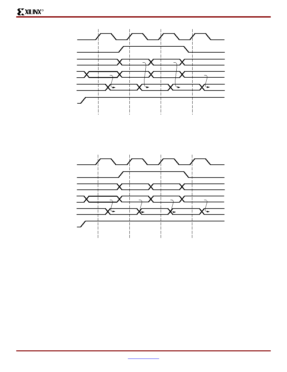
Spartan-3 1.2V FPGA Family: Functional Description
DS099-2 (v1.2) July 11, 2003
www.xilinx.com
17
Advance Product Specification
1-800-255-7778
R
Choosing the READ_FIRST attribute, data already stored in
the addressed location pass to the DO outputs before that
location is over-written with new data from the DI inputs on
an enabled active CLK edge. READ_FIRST timing is shown
in the portion of
Figure 10
during which WE is High.
Choosing a third attribute called NO_CHANGE puts the DO
outputs in a latched state when asserting WE. Under this
condition, the DO outputs will retain the data driven just
before WE was asserted. NO_CHANGE timing is shown in
the portion of
Figure 11
during which WE is High.
Figure 9: Waveforms of Block RAM Data Operations with WRITE_FIRST Selected
CLK
WE
DI
ADDR
DO
EN
DISABLED
READ
XXXX
1111
2222
XXXX
aa
bb
cc
dd
0000
MEM(aa)
1111
2222
MEM(dd)
READ
WRITE
MEM(bb)=1111
WRITE
MEM(cc)=2222
DS099-2_14_030403
Figure 10: Waveforms of Block RAM Data Operations with READ_FIRST Selected
CLK
WE
DI
ADDR
DO
EN
DISABLED
READ
XXXX
1111
2222
XXXX
aa
bb
cc
dd
0000
MEM(aa)
old MEM(bb)
old MEM(cc)
MEM(dd)
READ
WRITE
MEM(bb)=1111
WRITE
MEM(cc)=2222
DS099-2_15_030403
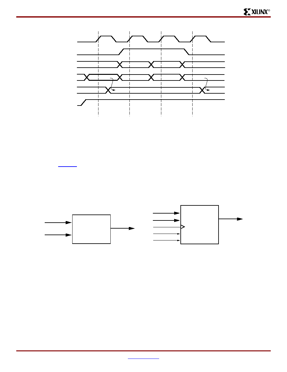
Spartan-3 1.2V FPGA Family: Functional Description
18
www.xilinx.com
DS099-2 (v1.2) July 11, 2003
1-800-255-7778
Advance Product Specification
40
R
Dedicated Multipliers
All Spartan-3 devices provide embedded multipliers that
accept two 18-bit words as inputs to produce a 36-bit prod-
uct. This section provides an introduction to multipliers. For
further details, see
XAPP467
: Using Embedded Multipliers
in Spartan-3 FPGAs.
The input buses to the multiplier accept data in two's-com-
plement form (either 18-bit signed or 17-bit unsigned). One
such multiplier is matched to each block RAM on the die.
The close physical proximity of the two ensures efficient
data handling. Cascading multipliers permits multiplicands
more than three in number as well as wider than 18-bits.
The multiplier is placed in a design using one of two primi-
tives: an asynchronous version called MULT18X18 and a
version with a register at the outputs called MULT18X18S,
as shown in
Figure 12a
and
Figure 12b
, respectively. The
signals for these primitives are defined in
Table 11
.
The CORE Generator system produces multipliers based
on these primitives that can be configured to suit a wide
range of requirements.
Figure 11: Waveforms of Block RAM Data Operations with NO_CHANGE Selected
CLK
WE
DI
ADDR
DO
EN
DISABLED
READ
XXXX
1111
2222
XXXX
aa
bb
cc
dd
0000
MEM(aa)
MEM(dd)
READ
WRITE
MEM(bb)=1111
WRITE
MEM(cc)=2222
DS099-2_16_030403
Figure 12: Embedded Multiplier Primitives
DS099-2_17_091302
(a) Asynchronous 18-bit Multiplier
(b) 18-bit Multiplier with Register at Outputs
A[17:0]
B[17:0]
P[35:0]
MULT18X18
A[17:0]
B[17:0]
CLK
CE
RST
P[35:0]
MULT18X18S

Spartan-3 1.2V FPGA Family: Functional Description
DS099-2 (v1.2) July 11, 2003
www.xilinx.com
19
Advance Product Specification
1-800-255-7778
R
Digital Clock Manager (DCM)
Spartan-3 devices provide flexible, complete control over
clock frequency, phase shift and skew through the use of
the DCM feature. To accomplish this, the DCM employs a
Delay-Locked Loop (DLL), a fully digital control system that
uses feedback to maintain clock signal characteristics with a
high degree of precision despite normal variations in oper-
ating temperature and voltage. This section provides a fun-
damental description of the DCM. For further information,
see
XAPP462
: Using Digital Clock Managers (DCMs) in
Spartan-3 FPGAs.
Each member of the Spartan-3 family has four DCMs,
except the smallest, the XC3S50, which has two DCMs.
The DCMs are located at the ends of the outermost Block
RAM column(s). See
Figure 1
in Module 1:
Introduction
and Ordering Information
. The Digital Clock Manager is
placed in a design as the "DCM" primitive.
The DCM supports three major functions:
�
Clock-skew Elimination: Clock skew describes the
extent to which clock signals may, under normal
circumstances, deviate from zero-phase alignment. It
occurs when slight differences in path delays cause the
clock signal to arrive at different points on the die at
different times. This clock skew can increase set-up
and hold time requirements as well as clock-to-out
time, which may be undesirable in applications
operating at a high frequency, when timing is critical.
The DCM eliminates clock skew by aligning the output
clock signal it generates with another version of the
clock signal that is fed back. As a result, the two clock
signals establish a zero-phase relationship. This
effectively cancels out clock distribution delays that
may lie in the signal path leading from the clock output
of the DCM to its feedback input.
�
Frequency Synthesis: Provided with an input clock
signal, the DCM can generate a wide range of different
output clock frequencies. This is accomplished by
either multiplying and/or dividing the frequency of the
input clock signal by any of several different factors.
�
Phase Shifting: The DCM provides the ability to shift
the phase of all its output clock signals with respect to
its input clock signal.
Table 11: Embedded Multiplier Primitives Descriptions
Signal
Name
Direction
Function
A[17:0]
Input
Apply one 18-bit multiplicand to these inputs. The MULT18X18S primitive requires a setup time
before the enabled rising edge of CLK.
B[17:0]
Input
Apply the other 18-bit multiplicand to these inputs. The MULT18X18S primitive requires a setup
time before the enabled rising edge of CLK.
P[35:0]
Output
The output on the P bus is a 36-bit product of the multiplicands A and B. In the case of the
MULT18X18S primitive, an enabled rising CLK edge updates the P bus.
CLK
Input
CLK is only an input to the MULT18X18S primitive. The clock signal applied to this input when
enabled by CE, updates the output register that drives the P bus.
CE
Input
CE is only an input to the MULT18X18S primitive. Enable for the CLK signal. Asserting this input
enables the CLK signal to update the P bus.
RST
Input
RST is only an input to the MULT18X18S primitive. Asserting this input resets the output register
on an enabled, rising CLK edge, forcing the P bus to all zeroes.
Notes:
1.
The control signals CLK, CE and RST have the option of inverted polarity.
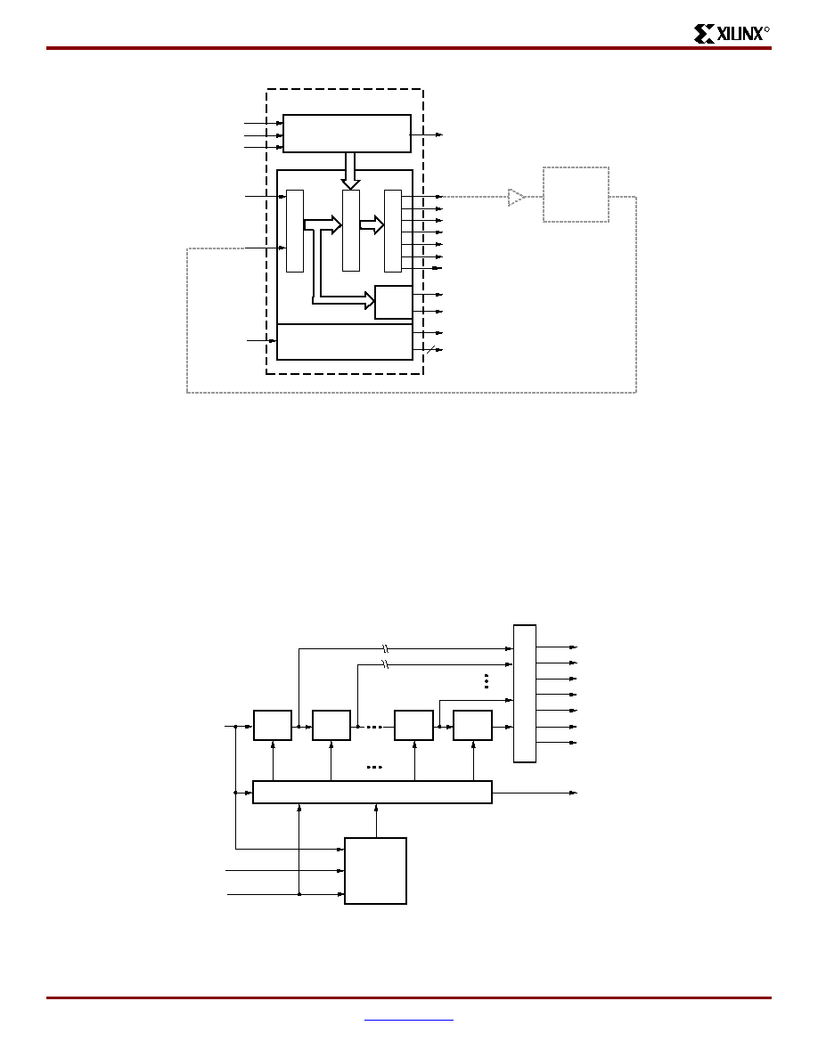
Spartan-3 1.2V FPGA Family: Functional Description
20
www.xilinx.com
DS099-2 (v1.2) July 11, 2003
1-800-255-7778
Advance Product Specification
40
R
The DCM has four functional components: the
Delay-Locked Loop (DLL), the Digital Frequency Synthe-
sizer (DFS), the Phase Shifter (PS), and the Status Logic.
Each component has its associated signals, as shown in
Figure 13
.
Delay-Locked Loop (DLL)
The most basic function of the DLL component is to elimi-
nate clock skew. The main signal path of the DLL consists of
an input stage, followed by a series of discrete delay ele-
ments or taps, which in turn leads to an output stage. This
path together with logic for phase detection and control
forms a system complete with feedback as shown in
Figure 14
.
Figure 13: DCM Functional Blocks and Associated Signals
DS099-2_07_040103
PSINCDEC
PSEN
PSCLK
CLKIN
CLKFB
RST
STATUS [7:0]
LOCKED
8
CLKFX180
CLKFX
CLK0
PSDONE
Clock
Distribution
Delay
CLK90
CLK180
CLK270
CLK2X
CLK2X180
CLKDV
Status
Logic
DFS
DLL
Phase
Shifter
Dela
y T
aps
Output Stage
Input Stage
DCM
Figure 14: Simplified Functional Diagram of DLL
DS099-2_08_041103
CLKIN
Delay
n
CLKFB
RST
CLK0
CLK90
CLK180
CLK270
CLK2X
CLK2X180
CLKDV
Output Section
Control
Delay
n-1
Phase
Detection
LOCKED
Delay
2
Delay
1
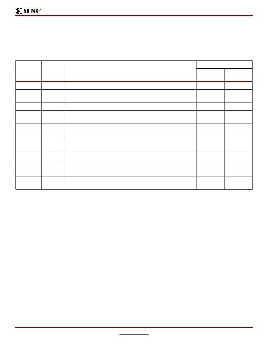
Spartan-3 1.2V FPGA Family: Functional Description
DS099-2 (v1.2) July 11, 2003
www.xilinx.com
21
Advance Product Specification
1-800-255-7778
R
The DLL component has two clock inputs, CLKIN and
CLKFB, as well as seven clock outputs, CLK0, CLK90,
CLK180, CLK270, CLK2X, CLK2X180, and CLKDV as
described in
Table 12
. The clock outputs drive simulta-
neously; however, the High Frequency mode only supports
a subset of the outputs available in the Low Frequency
mode. See
DLL Frequency Modes, page 23
. Signals that
initialize and report the state of the DLL are discussed in
The Status Logic Component, page 28
.
The clock signal supplied to the CLKIN input serves as a
reference waveform, with which the DLL seeks to align the
feedback signal at the CLKFB input. When eliminating clock
skew, the common approach to using the DLL is as follows:
The CLK0 signal is passed through the clock distribution
network to all the registers it synchronizes. These registers
are either internal or external to the FPGA. After passing
through the clock distribution network, the clock signal
returns to the DLL via a feedback line called CLKFB. The
control block inside the DLL measures the phase error
between CLKFB and CLKIN. This phase error is a measure
of the clock skew that the clock distribution network intro-
duces. The control block activates the appropriate number
of delay elements to cancel out the clock skew. Once the
DLL has brought the CLK0 signal in phase with the CLKIN
signal, it asserts the LOCKED output, indicating a "lock" on
to the CLKIN signal.
DLL Attributes and Related Functions
A number of different functional options can be set for the
DLL component through the use of the attributes described
in
Table 13
. Each attribute is described in detail in the sec-
tions that follow:
Table 12: DLL Signals
Signal
Direction
Description
Mode Support
Low
Frequency
High
Frequency
CLKIN
Input
Accepts original clock signal.
Yes
Yes
CLKFB
Input
Accepts either CLK0 or CLK2X as feed back signal. (Set
CLK_FEEDBACK attribute accordingly).
Yes
Yes
CLK0
Output
Generates clock signal with same frequency and phase as CLKIN.
Yes
Yes
CLK90
Output
Generates clock signal with same frequency as CLKIN, only
phase-shifted 90�.
Yes
No
CLK180
Output
Generates clock signal with same frequency as CLKIN, only
phase-shifted 180�.
Yes
Yes
CLK270
Output
Generates clock signal with same frequency as CLKIN, only
phase-shifted 270�.
Yes
No
CLK2X
Output
Generates clock signal with same phase as CLKIN, only twice the
frequency.
Yes
No
CLK2X180
Output
Generates clock signal with twice the frequency of CLKIN,
phase-shifted 180� with respect to CLKIN.
Yes
No
CLKDV
Output
Divides the CLKIN frequency by CLKDV_DIVIDE value to generate
lower frequency clock signal that is phase-aligned to CLKIN.
Yes
Yes
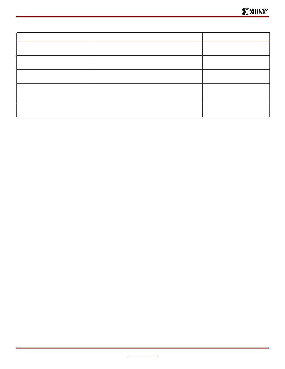
Spartan-3 1.2V FPGA Family: Functional Description
22
www.xilinx.com
DS099-2 (v1.2) July 11, 2003
1-800-255-7778
Advance Product Specification
40
R
DLL Clock Input Connections
An external clock source enters the FPGA using a Global
Clock Input Buffer (IBUFG), which directly accesses the glo-
bal clock network or an Input Buffer (IBUF). Clock signals
within the FPGA drive a global clock net using a Global
Clock Multiplexer Buffer (BUFGMUX). The global clock net
connects directly to the CLKIN input. The internal and exter-
nal connections are shown in
Figure 15a
and
Figure 15c
,
respectively. A differential clock (e.g., LVDS) can serve as
an input to CLKIN.
DLL Clock Output and Feedback Connections
As many as four of the nine DCM clock outputs can simulta-
neously drive the four BUFGMUX buffers on the same die
edge (top or bottom). All DCM clock outputs can simulta-
neously drive general routing resources, including intercon-
nect leading to OBUF buffers.
The feedback loop is essential for DLL operation and is
established by driving the CLKFB input with either the CLK0
or the CLK2X signal so that any undesirable clock distribu-
tion delay is included in the loop. It is possible to use either
of these two signals for synchronizing any of the seven DLL
outputs: CLK0, CLK90, CLK180, CLK270, CLKDV, CLK2X,
or CLK2X180. The value assigned to the CLK_FEEDBACK
attribute must agree with the physical feedback connection:
a value of 1X for the CLK0 case, 2X for the CLK2X case. If
the DCM is used in an application that does not require the
DLL -- i.e., only the DFS is used -- then there is no feed-
back loop so CLK_FEEDBACK is set to NONE.
There are two basic cases that determine how to connect
the DLL clock outputs and feedback connections: on-chip
synchronization and off-chip synchronization, which are
illustrated in
Figure 15a
through
Figure 15d
.
Table 13: DLL Attributes
Attribute
Description
Values
CLK_FEEDBACK
Chooses either the CLK0 or CLK2X output to drive the
CLKFB input
NONE, 1X, 2X
DLL_FREQUENCY_MODE
Chooses between High Frequency and Low
Frequency modes
LOW, HIGH
CLKIN_DIVIDE_BY_2
Halves the frequency of the CLKIN signal just as it
enters the DCM
TRUE, FALSE
CLKDV_DIVIDE
Selects constant used to divide the CLKIN input
frequency to generate the CLKDV output frequency
1.5, 2, 2.5, 3, 3.5, 4, 4.5, 5, 5.5,
6.0, 6.5, 7.0, 7.5, 8, 9, 10, 11,
12, 13, 14, 15, and 16.
DUTY_CYCLE_CORRECTION
Enables 50% duty cycle correction for the CLK0,
CLK90, CLK180, and CLK270 outputs
TRUE, FALSE
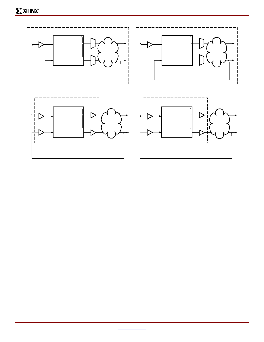
Spartan-3 1.2V FPGA Family: Functional Description
DS099-2 (v1.2) July 11, 2003
www.xilinx.com
23
Advance Product Specification
1-800-255-7778
R
In the on-chip synchronization case (
Figure 15a
and
Figure 15b
), it is possible to connect any of the DLL's seven
output clock signals through general routing resources to
the FPGA's internal registers. Either a Global Clock Buffer
(BUFG) or a BUFGMUX affords access to the global clock
network. As shown in
Figure 15a
, the feedback loop is cre-
ated by routing CLK0 (or CLK2X, in
Figure 15b
) to a global
clock net, which in turn drives the CLKFB input.
In the off-chip synchronization case (
Figure 15c
and
Figure 15d
), CLK0 (or CLK2X) plus any of the DLL's other
output clock signals exit the FPGA using output buffers
(OBUF) to drive an external clock network plus registers on
the board. As shown in
Figure 15c
, the feedback loop is
formed by feeding CLK0 (or CLK2X, in
Figure 15d
) back
into the FPGA using an IBUFG, which directly accesses the
global clock network, or an IBUF. Then, the global clock net
is connected directly to the CLKFB input.
DLL Frequency Modes
The DLL supports two distinct operating modes, High Fre-
quency and Low Frequency, with each specified over a differ-
ent clock frequency range. The DLL_FREQUENCY_MODE
attribute chooses between the two modes. When the
attribute is set to LOW, the Low Frequency mode permits all
seven DLL clock outputs to operate over a low-to-moderate
frequency range. When the attribute is set to HIGH, the High
Frequency mode allows the CLK0, CLK180 and CLKDV out-
puts to operate at the highest possible frequencies. The
remaining DLL clock outputs are not available for use in High
Frequency mode.
Accommodating High Input Frequencies
If the frequency of the CLKIN signal is high such that it
exceeds the maximum permitted, divide it down to an
acceptable value using the CLKIN_DIVIDE_BY_2 attribute.
When this attribute is set to TRUE, the CLKIN frequency is
divided by a factor of two just as it enters the DCM.
Coarse Phase Shift Outputs of the DLL Compo-
nent
In addition to CLK0 for zero-phase alignment to the CLKIN
signal, the DLL also provides the CLK90, CLK180 and
CLK270 outputs for 90�, 180� and 270� phase-shifted sig-
nals, respectively. These signals are described in
Table 12
.
Figure 15: Input Clock, Output Clock, and Feedback Connections for the DLL
DS099-2_09_071003
CLK90
CLK180
CLK270
CLKDV
CLK2X
CLK2X180
CLK0
CLK0
Clock
Net Delay
BUFGMUX
BUFGMUX
BUFG
FPGA
(a) On-Chip with CLK0 Feedback
CLKIN
DCM
CLKFB
CLK90
CLK180
CLK270
CLKDV
CLK2X
CLK2X180
CLK0
CLK0
Clock
Net Delay
IBUFG
IBUFG
FPGA
(c) Off-Chip with CLK0 Feedback
CLKIN
DCM
CLKFB
OBUFG
OBUFG
CLK2X
CLK2X
IBUFG
IBUFG
FPGA
(d) Off-Chip with CLK2X Feedback
CLKIN
DCM
CLKFB
OBUFG
OBUFG
CLK0
CLK90
CLK180
CLK270
CLKDV
CLK2X180
CLK2X
CLK2X
Clock
Net Delay
Clock
Net Delay
BUFGMUX
BUFGMUX
BUFG
FPGA
(b) On-Chip with CLK2X Feedback
CLKIN
DCM
CLKFB
CLK0
CLK90
CLK180
CLK270
CLKDV
CLK2X180
Notes:
1.
In the Low Frequency mode, all seven DLL outputs are available. In the High Frequency mode, only the CLK0, CLK180,
and CLKDV outputs are available.

Spartan-3 1.2V FPGA Family: Functional Description
24
www.xilinx.com
DS099-2 (v1.2) July 11, 2003
1-800-255-7778
Advance Product Specification
40
R
Their relative timing in the Low Frequency Mode is shown in
Figure 16
. The CLK90, CLK180 and CLK270 outputs are
not available when operating in the High Frequency mode.
(See the description of the DLL_FREQUENCY_MODE
attribute in
Table 13
.) For control in finer increments than
90�, see the
Phase Shifter (PS), page 26
section.
Basic Frequency Synthesis Outputs of the DLL
Component
The DLL component provides basic options for frequency
multiplication and division in addition to the more flexible
synthesis capability of the DFS component, described in a
later section. These operations result in output clock signals
with frequencies that are either a fraction (for division) or a
multiple (for multiplication) of the incoming clock frequency.
The CLK2X output produces an in-phase signal that is twice
the frequency of CLKIN. The CLK2X180 output also dou-
bles the frequency, but is 180� out-of-phase with respect to
CLKIN. The CLKDIV output generates a clock frequency
that is a predetermined fraction of the CLKIN frequency.
The CLKDV_DIVIDE attribute determines the factor used to
divide the CLKIN frequency. The attribute can be set to var-
ious values as described in
Table 13
. The basic frequency
synthesis outputs are described in
Table 12
. Their relative
timing in the Low Frequency Mode is shown in
Figure 16
.
The CLK2X and CLK2X180 outputs are not available when
operating in the High Frequency mode. (See the description
of the DLL_FREQUENCY_MODE attribute in
Table 14
.)
Duty Cycle Correction of DLL Clock Outputs
The CLK2X
(1)
, CLK2X180, and CLKDV
(2)
output signals
ordinarily exhibit a 50% duty cycle � even if the incoming
CLKIN signal has a different duty cycle. Fifty-percent duty
cycle means that the High and Low times of each clock
cycle are equal. The DUTY_CYCLE_CORRECTION
attribute determines whether or not duty cycle correction is
applied to the CLK0, CLK90, CLK180 and CLK270 outputs.
If DUTY_CYCLE_CORRECTION is set to TRUE, then the
duty cycle of these four outputs is corrected to 50%. If
DUTY_CYCLE_CORRECTION is set to FALSE, then these
outputs exhibit the same duty cycle as the CLKIN signal.
Figure 16
compares the characteristics of the DLL's output
signals to those of the CLKIN signal.
1. The CLK2X output generates a 25% duty cycle clock at the same frequency as the CLKIN signal until the DLL has achieved lock.
2. The duty cycle of the CLKDV outputs may differ somewhat from 50% (i.e., the signal will be High for less than 50% of the period) when
the CLKDV_DIVIDE attribute is set to a non-integer value and the DLL is operating in the High Frequency mode.
Figure 16: Characteristics of the DLL Clock Outputs
Output Signal - Duty Cycle is Always Corrected
Output Signal - Attribute Corrects Duty Cycle
Phase:
Input Signal (30% Duty Cycle)
0
o
90
o
180
o
270
o
0
o
90
o
180
o
270
o
0
o
DUTY_CYCLE_CORRECTION = FALSE
DUTY_CYCLE_CORRECTION = TRUE
DS099-2_10_031303
CLK2X
CLK2X180
CLKIN
CLKDV
(1)
CLK0
CLK90
CLK180
CLK270
CLK0
CLK90
CLK180
CLK270
t
Notes:
1.
The DLL attribute CLKDV_DIVIDE is set to 2.
Spartan-3 1.2V FPGA Family: Functional Description
DS099-2 (v1.2) July 11, 2003
www.xilinx.com
25
Advance Product Specification
1-800-255-7778
R
Digital Frequency Synthesizer (DFS)
The DFS component generates clock signals the frequency
of which is a product of the clock frequency at the CLKIN
input and a ratio of two user-determined integers. Because
of the wide range of possible output frequencies such a ratio
permits, the DFS feature provides still further flexibility than
the DLL's basic synthesis options as described in the pre-
ceding section. The DFS component's two dedicated out-
puts, CLKFX and CLKFX180, are defined in
Table 15
.
The signal at the CLKFX180 output is essentially an inver-
sion of the CLKFX signal. These two outputs always exhibit
a 50% duty cycle. This is true even when the CLKIN signal
does not. These DFS clock outputs are driven at the same
time as the DLL's seven clock outputs.
The numerator of the ratio is the integer value assigned to
the attribute CLKFX_MULTIPLY and the denominator is the
integer value assigned to the attribute CLKFX_DIVIDE.
These attributes are described in
Table 14
.
The output frequency (f
CLKFX
) can be expressed as a func-
tion of the incoming clock frequency (f
CLKIN
) as follows:
f
CLKFX
= f
CLKIN
*(CLKFX_MULTIPLY/CLKFX_DIVIDE) (3)
Regarding the two attributes, it is possible to assign any
combination of integer values, provided that two conditions
are met:
1.
The two values fall within their corresponding ranges,
as specified in
Table 14
.
2.
The f
CLKFX
frequency calculated from the above
expression accords with the DCM's operating frequency
specifications.
For example, if CLKFX_MULTIPLY = 5 and CLKFX_DIVIDE
= 3, then the frequency of the output clock signal would be
5/3 that of the input clock signal.
DFS Frequency Modes
The DFS supports two operating modes, High Frequency
and Low Frequency, with each specified over a different
clock frequency range. The DFS_FREQUENCY_MODE
attribute chooses between the two modes. When the
attribute is set to LOW, the Low Frequency mode permits
the two DFS outputs to operate over a low-to-moderate fre-
quency range. When the attribute is set to HIGH, the High
Frequency mode allows both these outputs to operate at the
highest possible frequencies.
DFS With or Without the DLL
The DFS component can be used with or without the DLL
component:
Without the DLL, the DFS component multiplies or divides
the CLKIN signal frequency according to the respective
CLKFX_MULTIPLY and CLKFX_DIVIDE values, generating
a clock with the new target frequency on the CLKFX and
CLKFX180 outputs. Though classified as belonging to the
DLL component, the CLKIN input is shared with the DFS
component. This case does not employ feedback loop;
therefore, it cannot correct for clock distribution delay.
With the DLL, the DFS operates as described in the preced-
ing case, only with the additional benefit of eliminating the
clock distribution delay. In this case, a feedback loop from
the CLK0 output to the CLKFB input must be present.
The DLL and DFS components work together to achieve
this phase correction as follows: Given values for the
CLKFX_MULTIPLY and CLKFX_DIVIDE attributes, the DLL
selects the delay element for which the output clock edge
coincides with the input clock edge whenever mathemati-
cally possible. For example, when CLKFX_MULTIPLY = 5
and CLKFX_DIVIDE = 3, the input and output clock edges
will coincide every three input periods, which is equivalent in
time to five output periods.
Smaller CLKFX_MULTIPLY and CLKFX_DIVIDE values
achieve faster lock times. With no factors common to the
two attributes, alignment will occur once with every number
of cycles equal to the CLKFX_DIVIDE value. Therefore, it is
recommended that the user reduce these values by factor-
ing wherever possible. For example, given
CLKFX_MULTIPLY = 9 and CLKFX_DIVIDE = 6, removing
a factor of three yields CLKFX_MULTIPLY = 3 and
CLKFX_DIVIDE = 2. While both value-pairs will result in the
multiplication of clock frequency by 3/2, the latter value-pair
will enable the DLL to lock more quickly.
Table 14: DFS Attributes
Attribute
Description
Values
DFS_FREQUENCY_MODE
Chooses between High Frequency and Low Frequency modes
Low, High
CLKFX_MULTIPLY
Frequency multiplier constant
Integer from 2 to 32
CLKFX_DIVIDE
Frequency divisor constant
Integer from 1 to 32
Table 15: DFS Signals
Signal
Direction
Description
CLKFX
Output
Multiplies the CLKIN frequency by the attribute-value ratio
(CLKFX_MULTIPLY/CLKFX_DIVIDE) to generate a clock signal with a new target frequency.
CLKFX180
Output
Generates a clock signal with same frequency as CLKFX, only shifted 180� out-of-phase.
Spartan-3 1.2V FPGA Family: Functional Description
26
www.xilinx.com
DS099-2 (v1.2) July 11, 2003
1-800-255-7778
Advance Product Specification
40
R
DFS Clock Output Connections
There are two basic cases that determine how to connect
the DFS clock outputs: on-chip and off-chip, which are illus-
trated in
Figure 15a
and
Figure 15c
, respectively. This is
similar to what has already been described for the DLL com-
ponent. See the
DLL Clock Output and Feedback Con-
nections, page 22
section.
In the on-chip case, it is possible to connect either of the
DFS's two output clock signals through general routing
resources to the FPGA's internal registers. Either a Global
Clock Buffer (BUFG) or a BUFGMUX affords access to the
global clock network. The optional feedback loop is formed
in this way, routing CLK0 to a global clock net, which in turn
drives the CLKFB input.
In the off-chip case, the DFS's two output clock signals, plus
CLK0 for an optional feedback loop, can exit the FPGA
using output buffers (OBUF) to drive a clock network plus
registers on the board. The feedback loop is formed by
feeding the CLK0 signal back into the FPGA using an
IBUFG, which directly accesses the global clock network, or
an IBUF. Then, the global clock net is connected directly to
the CLKFB input.
Phase Shifter (PS)
The DCM provides two approaches to controlling the phase
of a DCM clock output signal relative to the CLKIN signal:
First, there are nine clock outputs that employ the DLL to
achieve a desired phase relationship: CLK0, CLK90,
CLK180, CLK270, CLK2X, CLK2X180, CLKDV CLKFX, and
CLKFX180. These outputs afford "coarse" phase control.
The second approach uses the PS component described in
this section to provide a still finer degree of control. The PS
component accomplishes this by introducing a "fine phase
shift" (T
PS
) between the CLKFB and CLKIN signals inside
the DLL component. The user can control this fine phase
shift down to a resolution of 1/256 of a CLKIN cycle or one
tap delay (DCM_TAP), whichever is greater. When in use,
the PS component shifts the phase of all nine DCM clock
output signals together. If the PS component is used
together with a DCM clock output such as the CLK90,
CLK180, CLK270, CLK2X180 and CLKFX180, then the fine
phase shift of the former gets added to the coarse phase
shift of the latter.
PS Component Enabling and Mode Selection
The CLKOUT_PHASE_SHIFT attribute enables the PS
component for use in addition to selecting between two
operating modes. As described in
Table 16
, this attribute
has three possible values: NONE, FIXED and VARIABLE.
When CLKOUT_PHASE_SHIFT is set to NONE, the PS
component is disabled and its inputs, PSEN, PSCLK, and
PSINCDEC, must be tied to GND. The set of waveforms in
Figure 17a
shows the disabled case, where the DLL main-
tains a zero-phase alignment of signals CLKFB and CLKIN
upon which the PS component has no effect. The PS com-
ponent is enabled by setting the attribute to either the
FIXED or VARIABLE values, which select the Fixed Phase
mode and the Variable Phase mode, respectively. These
two modes are described in the sections that follow
Determining the Fine Phase Shift
The user controls the phase shift of CLKFB relative to
CLKIN by setting and/or adjusting the value of the
PHASE_SHIFT attribute. This value must be an integer
ranging from �255 to +255. The PS component uses this
value to calculate the desired fine phase shift (T
PS
) as a
fraction of the CLKIN period (T
CLKIN
). Given values for
PHASE-SHIFT and T
CLKIN
, it is possible to calculate T
PS
as
follows:
T
PS
= (PHASE_SHIFT/256)*T
CLKIN
(4)
Both the Fixed Phase and Variable Phase operating modes
employ this calculation. If the PHASE_SHIFT value is zero,
then CLKFB and CLKIN will be in phase, the same as when
the PS component is disabled. When the PHASE_SHIFT
value is positive, the CLKFB signal will be shifted later in
time with respect to CLKIN. If the attribute value is negative,
the CLKFB signal will be shifted earlier in time with respect
to CLKIN.
The Fixed Phase Mode
This mode fixes the desired fine phase shift to a fraction of
the T
CLKIN
, as determined by Equation (4) and its
user-selected PHASE_SHIFT value P. The set of wave-
forms in
Figure 17b
illustrates the relationship between
CLKFB and CLKIN in the Fixed Phase mode. In the Fixed
Phase mode, the PSEN, PSCLK and PSINCDEC inputs are
not used and must be tied to GND.
Table 16: PS Attributes
Attribute
Description
Values
CLKOUT_PHASE_SHIFT
Disables PS component or chooses between Fixed Phase
and Variable Phase modes.
NONE, FIXED, VARIABLE
PHASE_SHIFT
Determines size and direction of initial fine phase shift.
Integers from �255 to +255
(1)
Notes:
1.
The practical range of values will be less when T
CLKIN
> FINE_SHIFT_RANGE in the Fixed Phase mode, also when T
CLKIN
>
(FINE_SHIFT_RANGE)/2 in the Variable Phase mode. the FINE_SHIFT_RANGE represents the sum total delay of all taps.
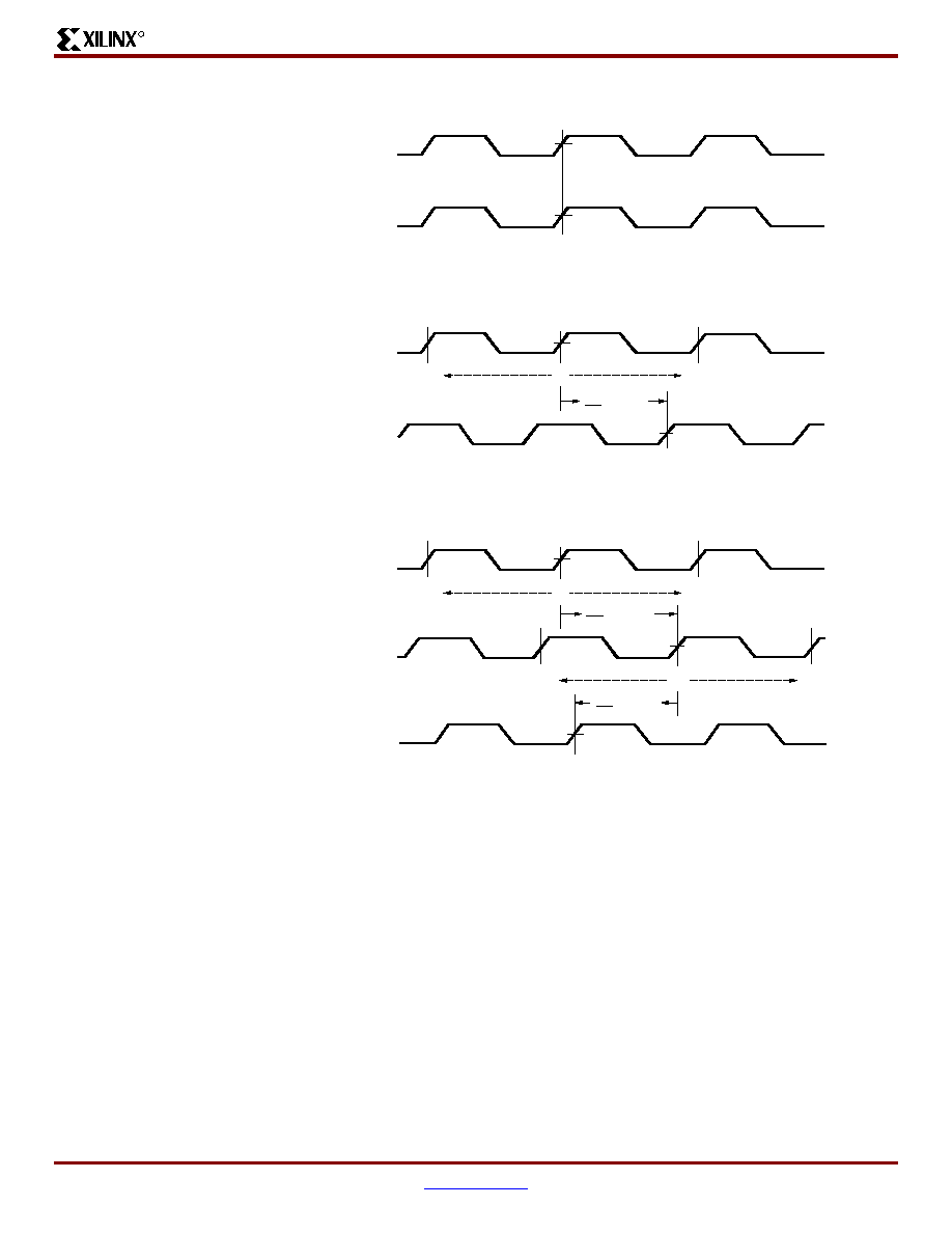
Spartan-3 1.2V FPGA Family: Functional Description
DS099-2 (v1.2) July 11, 2003
www.xilinx.com
27
Advance Product Specification
1-800-255-7778
R
Figure 17: Phase Shifter Waveforms
DS099-2_11_031303
CLKIN
CLKFB
* T
CLKIN
P
256
b. CLKOUT_PHASE_SHIFT = FIXED
* T
CLKIN
P
256
Shift Range over all P Values:
�255
+255
Shift Range over all P Values:
0
0
�255
+255
Shift Range over all N Values:
0
�255
+255
CLKIN
CLKFB before
Decrement
c. CLKOUT_PHASE_SHIFT = VARIABLE
CLKFB after
Decrement
* T
CLKIN
N
256
CLKIN
CLKFB
a. CLKOUT_PHASE_SHIFT = NONE
Notes:
1.
P represents the integer value ranging from �255 to +255 to which the PHASE_SHIFT attribute is assigned.
2.
N is an integer value ranging from �255 to +255 that represents the net phase shift effect from a series of increment and/or
decrement operations.
N = {Total number of increments} � {Total number of decrements}
A positive value for N indicates a net increment; a negative value indicates a net decrement.

Spartan-3 1.2V FPGA Family: Functional Description
28
www.xilinx.com
DS099-2 (v1.2) July 11, 2003
1-800-255-7778
Advance Product Specification
40
R
The Variable Phase Mode
The "Variable Phase" mode dynamically adjusts the fine
phase shift over time using three inputs to the PS compo-
nent, namely PSEN, PSCLK and PSINCDEC, as defined in
Table 17
.
Just following device configuration, the PS component ini-
tially determines T
PS
by evaluating Equation (4) for the
value assigned to the PHASE_SHIFT attribute. Then to
dynamically adjust that phase shift, use the three PS inputs
to increase or decrease the fine phase shift.
PSINCDEC is synchronized to the PSCLK clock signal,
which is enabled by asserting PSEN. It is possible to drive
the PSCLK input with the CLKIN signal or any other clock
signal. A request for phase adjustment is entered as follows:
For each PSCLK cycle that PSINCDEC is High, the PS
component adds 1/256 of a CLKIN cycle to T
PS
. Similarly,
for each enabled PSCLK cycle that PSINCDEC is Low, the
PS component subtracts 1/256 of a CLKIN cycle from T
PS
.
The phase adjustment may require as many as 100 CLKIN
cycles plus three PSCLK cycles to take effect, at which
point the output PSDONE goes High for one PSCLK cycle.
This pulse indicates that the PS component has finished the
present adjustment and is now ready for the next request.
Asserting the Reset (RST) input, returns T
PS
to its original
shift time, as determined by the PHASE_SHIFT attribute
value. The set of waveforms in
Figure 17c
illustrates the
relationship between CLKFB and CLKIN in the Variable
Phase mode.
The Status Logic Component
The Status Logic component not only reports on the state of
the DCM but also provides a means of resetting the DCM to
an initial known state. The signals associated with the Sta-
tus Logic component are described in
Table 18
.
As a rule, the Reset (RST) input is asserted only upon con-
figuring the device or changing the CLKIN frequency. A
DCM reset does not affect attribute values (e.g.,
CLKFX_MULTIPLY and CLKFX_DIVIDE). If not used, RST
must be tied to GND.
The eight bits of the STATUS bus are defined in
Table 19
.
Table 17: Signals for Variable Phase Mode
Signal
Direction
Description
PSEN
(1)
Input
Enables PSCLK for variable phase adjustment.
PSCLK
(1)
Input
Clock to synchronize phase shift adjustment.
PSINCDEC
(1)
Input
Chooses between increment and decrement for phase adjustment. It is synchronized to the
PSCLK signal.
PSDONE
Output
Goes High to indicate that present phase adjustment is complete and PS component is
ready for next phase adjustment request. It is synchronized to the PSCLK signal.
Notes:
1.
It is possible to program this input for either a true or inverted polarity
Table 18: Status Logic Signals
Signal
Direction
Description
RST
Input
A High resets the entire DCM to its initial power-on state. Initializes the DLL taps for a delay
of zero. Sets the LOCKED output Low. This input is asynchronous.
STATUS[7:0]
Output
The bit values on the STATUS bus provide information regarding the state of DLL and PS
operation
LOCKED
Output
Indicates that the CLKIN and CLKFB signals are in phase by going High. The two signals
are out-of-phase when Low.
Spartan-3 1.2V FPGA Family: Functional Description
DS099-2 (v1.2) July 11, 2003
www.xilinx.com
29
Advance Product Specification
1-800-255-7778
R
Stabilizing DCM Clocks Before User Mode
It is possible to delay the completion of device configuration
until after the DLL has achieved a lock condition using the
STARTUP_WAIT attribute described in
Table 20
. This
option ensures that the FPGA does not enter user mode --
i.e., begin functional operation -- until all system clocks
generated by the DCM are stable. In order to achieve the
delay, it is necessary to set the attribute to TRUE as well as
set the BitGen option LCK_cycle to one of the six cycles
making up the Startup phase of configuration. The selected
cycle defines the point at which configuration will halt until
the LOCKED output goes High.
Global Clock Network
Spartan-3 devices have eight Global Clock inputs called
GCLK0 - GCLK7. These inputs provide access to a
low-capacitance, low-skew network that is well-suited to
carrying high-frequency signals. The Spartan-3 clock net-
work is shown in
Figure 18
. GCLK0 through GCLK3 are
placed at the center of the die's bottom edge. GCLK4
through GCLK7 are placed at the center of the die's top
edge. It is possible to route each of the eight Global Clock
inputs to any CLB on the die.
Eight Global Clock Multiplexers (also called BUFGMUX ele-
ments) are provided that accept signals from Global Clock
inputs and route them to the internal clock network as well
as DCMs. Four BUFGMUX elements are placed at the cen-
ter of the die's bottom edge, just above the GCLK0 - GCLK4
inputs. The remaining four BUFGMUX elements are placed
at the center of the die's top edge, just below the GCLK4 -
GCLK7 inputs.
Each BUFGMUX element is a 2-to-1 multiplexer that can
receive signals from any of the four following sources:
1.
One of the four Global Clock inputs on the same side of
the die -- top or bottom -- as the BUFGMUX element in
use.
2.
Any of four nearby horizontal Double lines.
3.
Any of four outputs from the DCM in the right-hand
quadrant that is on the same side of the die as the
BUFGMUX element in use.
4.
Any of four outputs from the DCM in the left-hand
quadrant that is on the same side of the die as the
BUFGMUX element in use.
Sources 3 and 4 are not available on the XC3S50 die that
lacks DCMs.
Each BUFGMUX can switch incoming clock signals to two
possible destinations:
1.
The vertical spine belonging to the same side of the die
-- top or bottom -- as the BUFGMUX element in use.
The two spines -- top and bottom -- each comprise
four vertical clock lines, each running from one of the
Table 19: DCM STATUS Bus
Bit
Name
Description
0
Phase Shift
Overflow
A value of 1 indicates a phase shift overflow when one of two conditions occur:
�
Incrementing (or decrementing) TPS beyond 255/256 of a CLKIN cycle.
�
The DLL is producing its maximum possible phase shift (i.e., all delay taps are active).
(1)
1
CLKIN Activity
A value of 1 indicates that the CLKIN signal is not toggling. A value of 0 indicates toggling. This
bit functions only when the CLKFB input is connected.
(2)
2
Reserved
-
3
Reserved
-
4
Reserved
-
5
Reserved
-
6
Reserved
-
7
Reserved
-
Notes:
1.
The DLL phase shift with all delay taps active is specified as the parameter FINE_SHIFT_RANGE.
2.
If only the DFS clock outputs are used, but none of the DLL clock outputs, this bit will not go High when the CLKIN signal stops.
Table 20: Status Attributes
Attribute
Description
Values
STARTUP_WAIT
Delays transition from configuration to user mode until lock condition is achieved.
TRUE, FALSE
Spartan-3 1.2V FPGA Family: Functional Description
30
www.xilinx.com
DS099-2 (v1.2) July 11, 2003
1-800-255-7778
Advance Product Specification
40
R
BUFGMUX elements on the same side towards the
center of the die. At the center of the die, clock signals
reach the eight-line horizontal spine, which spans the
width of the die. In turn, the horizontal spine branches
out into a subsidiary clock interconnect that accesses
the CLBs.
2.
The clock input of either DCM on the same side of the
die -- top or bottom -- as the BUFGMUX element in
use.
A Global clock input is placed in a design using either a
BUFGMUX element or the BUFG (Global Clock Buffer) ele-
ment. For the purpose of minimizing the dynamic power dis-
sipation of the clock network, the Xilinx development
software automatically disables all clock line segments that
a design does not use.
Figure 18: Spartan-3 Clock Network (Top View)
4
4
4
4
4
4
4
8
8
4
4
8
8
Horizontal Spine
T
op Spine
Bottom Spine
4
DCM
DCM
DCM
DCM
Array Dependent
Array Dependent
�
�
�
�
�
�
�
�
�
�
�
�
DS099-2_18_070203
4 BUFGMUX
GCLK2
GCLK3
GCLK0
GCLK1
4 BUFGMUX
GCLK6
GCLK4
GCLK7
GCLK5
Spartan-3 1.2V FPGA Family: Functional Description
DS099-2 (v1.2) July 11, 2003
www.xilinx.com
31
Advance Product Specification
1-800-255-7778
R
Interconnect
Interconnect (or routing) passes signals among the various
functional elements of Spartan-3 devices. There are four
kinds of interconnect: Long lines, Hex lines, Double lines,
and Direct lines.
Long lines connect to one out of every six CLBs (see
Figure 19a
). Because of their low capacitance, these lines
are well-suited for carrying high-frequency signals with min-
imal loading effects (e.g. skew). If all eight Global Clock
Inputs are already committed and there remain additional
clock signals to be assigned, Long lines serve as a good
alternative.
Hex lines connect one out of every three CLBs (see
Figure 19b
). These lines fall between Long lines and Dou-
ble lines in terms of capability: Hex lines approach the
high-frequency characteristics of Long lines at the same
time, offering greater connectivity.
Double lines connect to every other CLB (see
Figure 19c
).
Compared to the types of lines already discussed, Double
lines provide a higher degree of flexibility when making con-
nections.
Direct lines afford any CLB direct access to neighboring
CLBs (see
Figure 19d
). These lines are most often used to
conduct a signal from a "source" CLB to a Double, Hex, or
Long line and then from the longer interconnect back to a
Direct line accessing a "destination" CLB.
Figure 19: Types of Interconnect
� � �
CLB
CLB
� � �
CLB
CLB
� � �
CLB
CLB
6
6
6
6
6
� � �
CLB
CLB
� � �
CLB
CLB
DS099-2_19_040103
(a) Long Line
CLB
CLB
CLB
CLB
CLB
CLB
CLB
8
DS099-2_20_040103
(b) Hex Line
CLB
2
CLB
CLB
DS099-2_21_040103
CLB
CLB
CLB
CLB
CLB
CLB
CLB
CLB
CLB
DS099-2_22_040103
(d) Direct Lines
(c) Double Line
Spartan-3 1.2V FPGA Family: Functional Description
32
www.xilinx.com
DS099-2 (v1.2) July 11, 2003
1-800-255-7778
Advance Product Specification
40
R
Configuration
Spartan-3 devices are configured by loading application
specific configuration data into the internal configuration
memory. Configuration is carried out using a subset of the
device pins, some of which are "Dedicated" to one function
only, while others, indicated by the term "Dual-Purpose",
can be re-used as general-purpose User I/Os once configu-
ration is complete.
Depending on the system design, several configuration
modes are supported, selectable via mode pins. The mode
pins M0, M1, and M2 are Dedicated pins. The mode pin set-
tings are shown in
Table 21
.
An additional pin, HSWAP_EN, is used in conjunction with
the mode pins to select whether user I/O pins have pull-ups
during configuration. By default, HSWAP_EN is tied High
(internal pull-up) which shuts off the pull-ups on the user I/O
pins during configuration. When HSWAP_EN is tied Low,
user I/Os have pull-ups during configuration. Other Dedi-
cated pins are CCLK (the configuration clock pin), DONE,
PROG_B, and the boundary-scan pins: TDI, TDO, TMS,
and TCK. Depending on the configuration mode chosen,
CCLK can be an output generated by the FPGA, or an input
accepting an externally generated clock.
A persist option is available which can be used to force the
configuration pins to retain their configuration function even
after device configuration is complete. If the persist option is
not selected then the configuration pins with the exception
of CCLK, PROG_B, and DONE can be used as user I/O in
normal operation. The persist option does not apply to the
boundary-scan related pins. The persist feature is valuable
in applications that readback configuration data after enter-
ing the User mode.
Table 22
lists the total number of bits required to configure
each FPGA as well as the PROMs suitable for storing those
bits. See
DS123
: Platform Flash In-System Programmable
Configuration PROMs data sheet for more information.
The Standard Configuration Interface
Configuration signals belong to one of two different catego-
ries: Dedicated or Dual-Purpose. Which category deter-
mines which of the FPGA's power rails supplies the signal's
driver and, thus, helps describe the electrical at the pin.
The Dedicated configuration pins include PROG_B,
HSWAP_EN, TDI, TMS, TCK, TDO, CCLK, DONE, and
M0-M2. These pins use the V
CCAUX
lines for power.
The Dual-Purpose configuration pins comprise INIT_B,
DOUT, BUSY, RDWR_B, CS_B, and DIN/D0-D7. Each of
these pins, according to its bank placement, uses the V
CCO
lines for either Bank 4 (VCCO_4) or Bank 5 (VCCO_5). All
the signals used in the serial configuration modes rely on
VCCO_4 power. Signals used in the parallel configuration
modes and Readback require from VCCO_5 as well as from
VCCO_4.
Both the Dedicated and Dual-Purpose signals described
above constitute the configuration interface. In the standard
case, this interface is 2.5V-LVCMOS-compatible. This
means that 2.5V is applied to the V
CCAUX
, VCCO_4, and
VCCO_5 lines (this last in the parallel or Readback case
only). One need only apply 2.5 Volts to these V
CCO
lines
from power-on to the end of configuration. Upon entering
the User mode, it is possible to switch to supply voltage per-
mitting signal swings other than 2.5V.
Table 21: Spartan-3 Configuration Mode Pin Settings
Configuration Mode
(1)
M0
M1
M2
Synchronizing Clock
Data Width
Serial DOUT
(2)
Master Serial
0
0
0
CCLK Output
1
Yes
Slave Serial
1
1
1
CCLK Input
1
Yes
Master Parallel
1
1
0
CCLK Output
8
No
Slave Parallel
0
1
1
CCLK Input
8
No
JTAG
1
0
1
TCK Input
1
No
Notes:
1.
The voltage levels on the M0, M1, and M2 pins select the configuration mode.
2.
The daisy chain is possible only in the Serial modes when DOUT is used.
Table 22: Spartan-3 Configuration Data
Device
File Sizes
Xilinx Platform Flash PROM
Serial
Configuration
Parallel
Configuration
XC3S50
439,264
XCF01S
XCF08P
XC3S200
1,047,616
XCF01S
XCF08P
XC3S400
1,699,136
XCF02S
XCF08P
XC3S1000
3,223,488
XCF04S
XCF08P
XC3S1500
5,214,784
XCF08P
XCF08P
XC3S2000
7,673,024
XCF08P
XCF08P
XC3S4000
11,316,864
XCF16P
XCF16P
XC3S5000
13,271,936
XCF16P
XCF16P

Spartan-3 1.2V FPGA Family: Functional Description
DS099-2 (v1.2) July 11, 2003
www.xilinx.com
33
Advance Product Specification
1-800-255-7778
R
3.3V-Tolerant Configuration Interface
It is possible to achieve 3.3V-tolerance at the configuration
interface simply by adding a few external resistors. This
approach may prove useful when it is undesirable to switch
the VCCO_4 and VCCO_5 voltages from 2.5V to 3.3V after
configuration.
The 3.3V-tolerance is implemented as follows (a similar
approach can be used for other supply voltage levels):
First, to power the Dual-Purpose configuration pins, apply
3.3V to the VCCO_4 and (as needed) the VCCO_5 lines.
This scales the output voltages and input thresholds associ-
ated with these pins so that they become 3.3V-compatible.
Second, to power the Dedicated configuration pins, apply
2.5V to the V
CCAUX
lines (the same as for the standard
interface). In order to achieve 3.3V-tolerance, the Dedicated
inputs will require series resistors that limit the incoming
current to 10mA or less. The Dedicated outputs will need
pull-up resistors to ensure adequate noise margin when the
FPGA is driving a High logic level into another device's 3.3V
receiver. Choose a power regulator or supply that can toler-
ate reverse current on the V
CCAUX
lines.
Configuration Modes
Spartan-3 supports the following five configuration modes:
�
Slave Serial mode
�
Master Serial mode
�
Slave Parallel
mode
�
Master Parallel mode
�
Boundary-Scan (JTAG) mode (IEEE 1532/IEEE
1149.1)
Slave Serial Mode
In Slave Serial mode, the FPGA receives configuration data
in bit-serial form from a serial PROM or other serial source
of configuration data. The FPGA on the far right of
Figure 20
is set for the Slave Serial mode. The CCLK pin on the FPGA
is an input in this mode. The serial bitstream must be setup
at the DIN input pin a short time before each rising edge of
the externally generated CCLK.
Multiple FPGAs can be daisy-chained for configuration from
a single source. After a particular FPGA has been config-
ured, the data for the next device is routed internally to the
DOUT pin. The data on the DOUT pin changes on the rising
edge of CCLK.
Figure 20: Connection Diagram for Master and Slave Serial Configuration
DOUT
DIN
CCLK
DONE
INIT_B
Spartan-3
FPGA
Master
PROG_B
DIN
CCLK
DONE
INIT_B
Spartan-3
FPGA
Slave
PROG_B
DS099_23_041103
D0
CLK
CE
OE/RESET
CF
Platform
Flash PROM
XCF0xS
or
XCFxxP
V
CCINT
1.2V
V
CCAUX
V
CCO
Bank 4
2.5V
2.5V
4.7K
All
2.5V
V
CCAUX
V
CCINT
V
CCO
Bank 4
1.2V
3.3V
V
CC
V
CCJ
V
CCO
2.5V
2.5V
M0
M1
M2
M0
M1
M2
GND
GND
GND
Notes:
1.
There are two ways to use the DONE line. First, one may set the BitGen option DriveDone to "Yes" only for the
last FPGA to be configured in the chain shown above (or for the single FPGA as may be the case). This enables
the DONE pin to drive High; thus, no pull-up resistor is necessary. DriveDone is set to "No" for the remaining
FPGAs in the chain. Second, DriveDone can be set to "No" for all FPGAs. Then all DONE lines are open-drain
and require the pull-up resistor shown in grey. In most cases, a value between 3.3K
to 4.7K is sufficient.
However, when using DONE synchronously with a long chain of FPGAs, cumulative capacitance may
necessitate lower resistor values (e.g. down to 330
) in order to ensure a rise time within one clock cycle.
2.
For information on how to program the FPGA using 3.3V signals and power, see
3.3V-Tolerant Configuration
Interface
.

Spartan-3 1.2V FPGA Family: Functional Description
34
www.xilinx.com
DS099-2 (v1.2) July 11, 2003
1-800-255-7778
Advance Product Specification
40
R
Slave Serial mode is selected by applying <111> to the
mode pins (M0, M1, and M2). A weak pull-up on the mode
pins makes slave serial the default mode if the pins are left
unconnected.
Master Serial Mode
In Master Serial mode, the CCLK pin is an output pin. The
FPGA just to the right of the PROM in
Figure 20
is set for
Master Serial mode. It is the FPGA that drives the configu-
ration clock on the CCLK pin to a Xilinx Serial PROM which
in turn feeds bit-serial data to the DIN input. The FPGA
accepts this data on each rising CCLK edge. After the
FPGA has been loaded, the data for the next device in a
daisy-chain is presented on the DOUT pin after the rising
CCLK edge.
The interface is identical to slave serial except that an inter-
nal oscillator is used to generate the configuration clock
(CCLK). A wide range of frequencies can be selected for
CCLK which always starts at a default frequency of 6 MHz.
Configuration bits then switch CCLK to a higher frequency
for the remainder of the configuration.
Slave Parallel Mode
The Parallel modes support the fastest configuration.
Byte-wide data is written into the FPGA with a BUSY flag
controlling the flow of data. An external source provides
8-bit-wide data, CCLK, an active-Low Chip Select (CS_B)
signal and an active-Low Write signal (RDWR_B). If BUSY
is asserted (High) by the FPGA, the data must be held until
BUSY goes Low. Data can also be read using the Slave
Parallel
mode. If RDWR_B is asserted, configuration data is
read out of the FPGA as part of a readback operation.
After configuration, it is possible to use any of the Multipur-
pose pins (DIN/D0-D7, DOUT/BUSY, INITB, CS_B, and
RDWR_B) as User I/Os. To do this, simply set the BitGen
option Persist to No and assign the desired signals to multi-
purpose configuration pins using the Xilinx development
software. Alternatively, it is possible to continue using the
configuration port (e.g. all configuration pins taken together)
when operating in the User mode. This is accomplished by
setting the Persist option to Yes.
Multiple FPGAs can be configured using the Slave Parallel
mode and can be made to start-up simultaneously.
Figure 21
shows the device connections. To configure mul-
tiple devices in this way, wire the individual CCLK, Data,
RDWR_B, and BUSY pins of all the devices in parallel. The
individual devices are loaded separately by deasserting the
CS_B pin of each device in turn and writing the appropriate
data.
Spartan-3 1.2V FPGA Family: Functional Description
DS099-2 (v1.2) July 11, 2003
www.xilinx.com
35
Advance Product Specification
1-800-255-7778
R
Figure 21: Connection Diagram for Slave Parallel Configuration
PROG_B
INIT_B
DONE
Spartan-3
Slave
INIT_B
D[0:7]
CCLK
RDWR_B
BUSY
CS_B
PROG_B
DONE
CS_B
Spartan-3
Slave
INIT_B
GND
D[0:7]
CCLK
RDWR_B
BUSY
CS_B
D[0:7]
CCLK
RDWR_B
BUSY
PROG_B
DONE
CS_B
DS099_24_041103
2.5V
M1
M2
M0
2.5V
M1
M2
M0
2.5V
V
CCAUX
V
CCO
Banks 4 & 5
V
CCINT
1.2V
4.7K
4.7K
2.5V
V
CCAUX
V
CCO
Banks 4 & 5
V
CCINT
1.2V
2.5V
GND
Notes:
1.
There are two ways to use the DONE line. First, one may set the BitGen option DriveDone to "Yes" only for the last FPGA
to be configured in the chain shown above (or for the single FPGA as may be the case). This enables the DONE pin to drive
High; thus, no pull-up resistor is necessary. DriveDone is set to "No" for the remaining FPGAs in the chain. Second,
DriveDone can be set to "No" for all FPGAs. Then all DONE lines are open-drain and require the pull-up resistor shown in
grey. In most cases, a value between 3.3K
to 4.7K is sufficient. However, when using DONE synchronously with a long
chain of FPGAs, cumulative capacitance may necessitate lower resistor values (e.g. down to 330
) in order to ensure a rise
time within one clock cycle.
2.
If the FPGAs use different configuration data files, configure them in sequence by first asserting the CS_B of one FPGA then
asserting the CS_B of the other FPGA.
3.
For information on how to program the FPGA using 3.3V signals and power, see
3.3V-Tolerant Configuration Interface
.
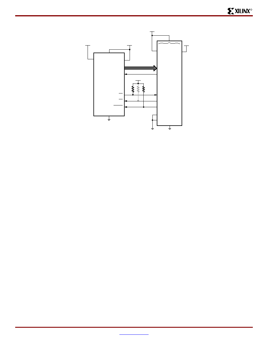
Spartan-3 1.2V FPGA Family: Functional Description
36
www.xilinx.com
DS099-2 (v1.2) July 11, 2003
1-800-255-7778
Advance Product Specification
40
R
Master Parallel Mode
In this mode, the device is configured byte-wide on a CCLK
supplied by the FPGA. Timing is similar to the Slave Parallel
mode except that CCLK is supplied by the FPGA. The
device connections are shown in
Figure 22
.
Boundary-Scan (JTAG) Mode
In Boundary-Scan mode, dedicated pins are used for con-
figuring the FPGA. The configuration is done entirely
through the IEEE 1149.1 Test Access Port (TAP). FPGA
configuration using the Boundary-Scan mode is compliant
with the IEEE 1149.1-1993 standard and the new IEEE
1532 standard for In-System Configurable (ISC) devices.
Configuration through the boundary-scan port is always
available, independent of the mode selection. Selecting the
Boundary-Scan mode simply turns off the other modes.
Configuration Sequence
The configuration of Spartan-3 devices is a three-stage pro-
cess that occurs after Power-On Reset or the assertion of
PROG_B. POR occurs after the V
CCINT
, V
CCAUX
, and V
CCO
Bank 4 supplies have reached their respective maximum
input threshold levels (see
Table 6
in Module 3:
DC and
Switching Characteristics
). After POR, the three-stage
process begins.
First, the configuration memory is cleared. Next, con-
figuration data is loaded into the memory, and finally, the
logic is activated by a start-up process. A flow diagram for
the configuration sequence of the Serial and Parallel modes
is shown in
Figure 23
. The flow diagram for the Bound-
ary-Scan configuration sequence appears in
Figure 24
.
Figure 22: Connection Diagram for Master Parallel Configuration
Spartan-3
Master
D[0:7]
CCLK
PROG_B
DONE
INIT_B
DATA[0:7]
CCLK
RDWR_B
CS_B
CF
CE
OE/RESET
Platform Flash
PROM
DS099_25_041103
2.5V
V
CCAUX
V
CCO
Banks 4 & 5
V
CCINT
1.2V
GND
GND
3.3V
V
CC
V
CCJ
V
CCO
2.5V
XCFxxP
2.5V
All
4.7K
Notes:
1.
There are two ways to use the DONE line. First, one may set the BitGen option DriveDone to "Yes"
only for the last FPGA to be configured in the chain shown above (or for the single FPGA as may be
the case). This enables the DONE pin to drive High; thus, no pull-up resistor is necessary. DriveDone
is set to "No" for the remaining FPGAs in the chain. Second, DriveDone can be set to "No" for all
FPGAs. Then all DONE lines are open-drain and require the pull-up resistor shown in grey. In most
cases, a value between 3.3K
to 4.7K is sufficient. However, when using DONE synchronously
with a long chain of FPGAs, cumulative capacitance may necessitate lower resistor values (e.g.
down to 330
) in order to ensure a rise time within one clock cycle.
Spartan-3 1.2V FPGA Family: Functional Description
DS099-2 (v1.2) July 11, 2003
www.xilinx.com
37
Advance Product Specification
1-800-255-7778
R
Figure 23: Configuration Flow Diagram for the Serial and Parallel Modes
Sample mode pins
No
No
No
Yes
Yes
Yes
Clear configuration
memory
Power-On
Set PROG_B Low
after Power-On
Yes
No
CRC
correct?
Yes
No
Reconfigure?
Load configuration
data frames
INIT_B goes Low.
Abort Start-Up
Start-Up
sequence
User mode
INIT_ B = High?
PROG_B = Low
DS099_26_041103
V
CCINT
>1V
and V
CCAUX
> 2V
and V
CCO
Bank 4 > 1V
Spartan-3 1.2V FPGA Family: Functional Description
38
www.xilinx.com
DS099-2 (v1.2) July 11, 2003
1-800-255-7778
Advance Product Specification
40
R
Figure 24: Boundary-Scan Configuration Flow Diagram
Sample
mode pins
(JTAG port becomes
available)
Clear
configuration
memory
No
No
No
Yes
Yes
Yes
Yes
No
Yes
Power-On
CRC
correct?
Load CFG_IN
instruction
Shutdown
sequence
Reconfigure?
Load JSTART
instruction
Synchronous
TAP reset
(Clock five 1's
on TMS)
Start-Up
sequence
User mode
INIT_B = High?
PROG_B = Low
Load
JShutdown
instruction
No
DS099_27_041103
Load configuration
data frames
V
CCINT
>1V
and V
CCAUX
> 2V
and V
CCO
Bank 4 > 1V
INIT_B goes Low.
Abort Start-Up
Set PROG_B Low
after Power-On
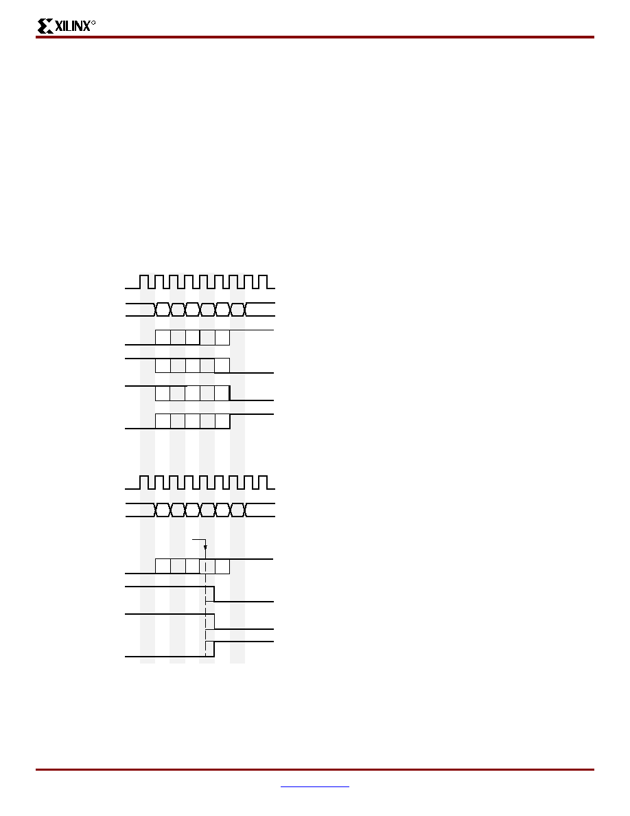
Spartan-3 1.2V FPGA Family: Functional Description
DS099-2 (v1.2) July 11, 2003
www.xilinx.com
39
Advance Product Specification
1-800-255-7778
R
Configuration is automatically initiated after power-on
unless it is delayed by the user. INIT_B is an open-drain line
that the FPGA holds Low during the clearing of the configu-
ration memory. Extending the time that the pin is Low
causes the configuration sequencer to wait. Thus, configu-
ration is delayed by preventing entry into the phase where
data is loaded.
The configuration process can also be initiated by asserting
the PROG_B pin. The end of the memory-clearing phase is
signaled by the INIT_B pin going High. At this point, the con-
figuration data is written to the FPGA. The FPGA holds the
Global Set/Reset (GSR) signal active throughout configura-
tion, keeping all flip-flops on the device in a reset state. The
completion of the entire process is signaled by the DONE
pin going High.
The default start-up sequence, shown in
Figure 25
, serves
as a transition to the User mode. The default start-up
sequence is that one CCLK cycle after DONE goes High,
the Global Three-State signal (GTS) is released. This per-
mits device outputs to which signals have been assigned to
become active. One CCLK cycle later, the Global Write
Enable (GWE) signal is released. This permits the internal
storage elements to begin changing state in response to the
design logic and the user clock.
The relative timing of configuration events can be changed
via the BitGen options in the Xilinx development software. In
addition, the GTS and GWE events can be made depen-
dent on the DONE pins of multiple devices all going High,
forcing the devices to start synchronously. The sequence
can also be paused at any stage, until lock has been
achieved on any DCM.
Readback
Using Slave Parallel mode, configuration data from the
FPGA can be read back. Readback is supported only in the
Slave Parallel
and Boundary-Scan modes.
Along with the configuration data, it is possible to read back
the contents of all registers, distributed SelectRAM, and
block RAM resources. This capability is used for real-time
debugging.
Figure 25: Default Start-Up Sequence
Start-Up Clock
Default Cycles
Sync-to-DONE
0
1
2
3
4
5
6
7
0
1
DONE High
2
3
4
5
6
7
Phase
Start-Up Clock
Phase
DONE
GTS
GSR
GWE
DS099_028_040803
DONE
GTS
GSR
GWE
Notes:
1.
The BitGen option StartupClk in the Xilinx
development software selects the CCLK input,
TCK input, or a user-designated global clock input
(the GCLK0 - GCLK7 pins) for receiving the clock
signal that synchronizes Start-Up.
Spartan-3 1.2V FPGA Family: Functional Description
40
www.xilinx.com
DS099-2 (v1.2) July 11, 2003
1-800-255-7778
Advance Product Specification
40
R
Revision History
The Spartan-3 Family Data Sheet
DS099-1, Spartan-3 1.2V FPGA Family:
Introduction and Ordering Information
(Module 1)
DS099-2, Spartan-3 1.2V FPGA Family: Functional Description (Module 2)
DS099-3, Spartan-3 1.2V FPGA Family:
DC and Switching Characteristics
(Module 3)
DS099-4, Spartan-3 1.2V FPGA Family:
Pinout Descriptions
(Module 4)
Date
Version No.
Description
04/11/03
1.0
Initial Xilinx release
05/19/03
1.1
Added Block RAM column, DCMs, and multipliers to XC3S50 descriptions.
07/11/03
1.2
Explained the configuration port Persist option in
Slave Parallel Mode
section. Updated
Figure 2
and
Double-Data-Rate Transmission
section to indicate that DDR clocking for the
XCS350 is the same as that for all other Spartan-3 devices. Updated description of I/O voltage
tolerance in
ESD Protection
section. In
Table 6
, changed input termination type for DCI
version of the LVCMOS standard to None. Added additional flexibility for making DLL
connections in
Figure 15
and accompanying text. In the
Configuration
section, inserted an
explanation of how to choose power supplies for the configuration interface, including
guidelines for achieving 3.3V-tolerance.

DS099-3 (v1.1) July 11, 2003
www.xilinx.com
1
Advance Product Specification
1-800-255-7778
� 2003 Xilinx, Inc. All rights reserved. All Xilinx trademarks, registered trademarks, patents, and disclaimers are as listed at
http://www.xilinx.com/legal.htm
.
All other trademarks and registered trademarks are the property of their respective owners. All specifications are subject to change without notice.
DC Electrical Characteristics
In this section, some specifications may be designated as
Advance or Preliminary. These terms are defined as fol-
lows:
Advance: Initial estimates based on simulation and/or
extrapolation from the characteristics of other families. Val-
ues are subject to change. Use as estimates, not for pro-
duction.
Preliminary: Based on characterization. Further changes
are not expected.
All specifications are representative of worst-case supply
voltage and junction temperature conditions. All specifica-
tions are subject to change without notice.
DC and AC characteristics are specified using the same
numbers for both commercial and industrial grades unless
otherwise noted.
014
Spartan-3 1.2V FPGA Family:
DC
and Switching Characteristics
DS099-3 (v1.1) July 11, 2003
0
0
Advance Product Specification
R
Table 1: Absolute Maximum Ratings
(1, 2)
Symbol
Description Min
Max
Units
V
CCINT
Internal supply voltage
�0.5
1.32
V
V
CCAUX
Auxiliary supply voltage
�0.5
3.00
V
V
CCO
Output driver supply voltage
�0.5
3.75
V
V
REF
Input reference voltage
�0.5
V
CCO
+ 0.5
V
V
IN
Voltage applied to bidirectional I/O
pins as well as unidirectional input
and output pins.
(3)
If present,
driver is put in a high-impedance
state.
V
CCO
3.0V
(4)
�0.5
V
CCO
+ 0.5
V
V
CCO
> 3.0V
�0.3
3.75
V
T
J
Operating junction temperature
V
CCO
3.0V
(4)
-
125
� C
V
CCO
> 3.0V
-
105
� C
T
SOL
(5)
Soldering temperature
-
220
� C
T
STG
Storage temperature
�65
150
� C
Notes:
1.
Stresses beyond those listed under Absolute Maximum Ratings will cause permanent damage to the device. These are stress
ratings only; functional operation of the device at these or any other conditions beyond those listed under the Recommended
Operating Conditions is not implied. Exposure to Absolute Maximum Ratings conditions for extended periods of time adversely
affects device reliability.
2.
All parameters representing voltages are measured with respect to GND unless otherwise specified.
3.
This specification applies to all User I/O, Multi-Function, and Dedicated pins.
4.
When V
CCO
is 3.0 V or less, V
IN
overshoot may go as high as V
CCO
+ 1.0 V for up to 11 ns provided that the current entering the I/O
pin is limited to 10 mA. Also, when V
CCO
is 3.0 V or less, V
IN
undershoot may go as low as �1.0 V for up to 11 ns provided that the
current entering the I/O pin is limited to 10 mA.
5.
For soldering guidelines, see the information on "Packaging and Thermal Characteristics" at
www.xilinx.com
.

Spartan-3 1.2V FPGA Family: DC and Switching Characteristics
2
www.xilinx.com
DS099-3 (v1.1) July 11, 2003
1-800-255-7778
Advance Product Specification
R
Table 2: Supply Voltage Thresholds for Power-On Reset
Symbol
Description
Min
Max
Units
V
CCINTT
Threshold for the V
CCINT
supply
0.4
1.0
V
V
CCAUXT
Threshold for the V
CCAUX
supply
0.8
2.0
V
V
CCO4T
Threshold for the V
CCO
Bank 4 supply
0.4
1.0
V
Notes:
1.
V
CCINT
, V
CCAUX
, and V
CCO
supplies may be applied in any order.
2.
During power-on, when the V
CCINT
, V
CCO
Bank 4, and V
CCAUX
voltages are rising, none may dip at any point within their respective
threshold-voltage ranges.
3.
All parameters representing voltages are measured with respect to GND unless otherwise specified.
Table 3: Power Voltage Levels Necessary for Preserving RAM Contents
(1)
Symbol
Description
Min
Units
V
DRINT
V
CCINT
level required to retain RAM data
1.0
V
V
DRAUX
V
CCAUX
level required to retain RAM data
2.0
V
Notes:
1.
RAM contents include configuration data.
2.
All parameters representing voltages are measured with respect to GND unless otherwise specified.
3.
The level of the V
CCO
supply has no effect on data retention.
Table 4: General Recommended Operating Conditions
Symbol
Description
Min
Nom
Max
Units
T
J
Junction temperature
Commercial
0
-
85
� C
Industrial
�40
-
100
� C
V
CCINT
Internal supply voltage
1.140
1.200
1.260
V
V
CCO
(1)
Output driver supply voltage
1.140
-
3.450
V
V
CCAUX
Auxiliary supply voltage
2.375
2.500
2.625
V
Notes:
1.
The V
CCO
range given here spans the lowest and highest operating voltages of all supported I/O standards. The recommended
V
CCO
range specific to each of the single-ended I/O standards is given in
Table 7
, and that specific to the differential standards is
given in
Table 9
.
2.
All parameters representing voltages are measured with respect to GND unless otherwise specified.
Spartan-3 1.2V FPGA Family: DC and Switching Characteristics
DS099-3 (v1.1) July 11, 2003
www.xilinx.com
3
Advance Product Specification
1-800-255-7778
14
R
Table 5: General DC Characteristics of User I/O, Multi-Function, and Dedicated Pins
Symbol
Description
Test Conditions
Min
Nom
Max
Units
I
L
Leakage current at User
I/O, Multi-Function, and
Dedicated pins
Driver is in a high-impedance
state
�10
-
+10
�A
I
RPU
Current through pull-up
resistor at User I/O,
Multi-Function, and
Dedicated pins
V
IN
= 0V
V
CCO
= 3.3V
500
1000
2000
�A
V
CCO
= 3.0V
400
800
1600
�A
V
CCO
= 2.5V
250
530
1100
�A
V
CCO
= 1.8V
120
270
770
�A
V
CCO
= 1.5V
70
180
440
�A
V
CCO
= 1.2V
40
100
300
�A
I
RPD
Current through
pull-down resistor at User
I/O, Multi-Function, and
Dedicated pins
V
IN
= V
CCO
= 3.3V
250
520
1100
�A
V
IN
= V
CCO
= 3.0V
250
520
1100
�A
V
IN
= V
CCO
= 2.5V
250
520
1100
�A
V
IN
= V
CCO
= 1.8V
250
520
1100
�A
V
IN
= V
CCO
= 1.5V
240
510
1100
�A
V
IN
= V
CCO
= 1.2V
230
480
1000
�A
I
REF
V
REF
current per pin
�10
-
+10
�A
C
IN
Input capacitance
5
-
11
pF
Notes:
1.
The numbers in this table are guaranteed over the conditions set forth in
Table 4
.

Spartan-3 1.2V FPGA Family: DC and Switching Characteristics
4
www.xilinx.com
DS099-3 (v1.1) July 11, 2003
1-800-255-7778
Advance Product Specification
R
Table 6: Quiescent Supply Current Characteristics
Symbol
Description
Device
Commercial
Industrial
Units
Typ
Max
Typ
Max
I
CCINTQ
Quiescent V
CCINT
supply
current
XC3S50
10
mA
XC3S200
mA
XC3S400
mA
XC3S1000
40
mA
XC3S1500
mA
XC3S2000
mA
XC3S4000
mA
XC3S5000
mA
I
CCOQ
Quiescent V
CCO
supply current
XC3S50
1.5
mA
XC3S200
mA
XC3S400
mA
XC3S1000
1.5
mA
XC3S1500
mA
XC3S2000
mA
XC3S4000
mA
XC3S5000
mA
I
CCAUXQ
Quiescent V
CCAUX
supply
current
XC3S50
7.0
mA
XC3S200
mA
XC3S400
mA
XC3S1000
25.0
mA
XC3S1500
mA
XC3S2000
mA
XC3S4000
mA
XC3S5000
mA
Notes:
1.
Quiescent supply current is measured with all I/O drivers in a high-impedance state and with all pull-up/pull-down resistors at the I/O
pads disabled. For typical values, the ambient temperature (T
A
) is 85 �C with V
CCINT
= 1.2V, V
CCO
= 2.5V, and V
CCAUX
= 2.5V.
2.
The numbers in this table are guaranteed over the conditions set forth in
Table 4
.
Spartan-3 1.2V FPGA Family: DC and Switching Characteristics
DS099-3 (v1.1) July 11, 2003
www.xilinx.com
5
Advance Product Specification
1-800-255-7778
14
R
Table 7: Recommended Operating Conditions for User I/Os Using Single-Ended Standards
Signal Standard
V
CCO
V
REF
V
IL
V
IH
Min (V)
Nom (V)
Max (V)
Min (V)
Nom (V)
Max (V)
Max (V)
Min (V)
GTL
-
-
-
0.74
0.8
0.86
V
REF
- 0.05
V
REF
+ 0.05
GTL_DCI
(2)
-
1.2
-
0.74
0.8
0.86
V
REF
- 0.05
V
REF
+ 0.05
GTLP
-
-
-
0.88
1
1.12
V
REF
- 0.1
V
REF
+ 0.1
GTLP_DCI
(2)
-
1.5
-
0.88
1
1.12
V
REF
- 0.1
V
REF
+ 0.1
HSTL_I,
HSTL_I_DCI
1.4
1.5
1.6
0.68
0.75
0.9
V
REF
- 0.1
V
REF
+ 0.1
HSTL_III,
HSTL_III_DCI
1.4
1.5
1.6
0.68
0.9
0.9
V
REF
- 0.1
V
REF
+ 0.1
HSTL_I_18,
HSTL_I_DCI_18
1.7
1.8
1.9
-
0.9
-
V
REF
- 0.1
V
REF
+ 0.1
HSTL_II_18,
HSTL_II_DCI_18
1.7
1.8
1.9
-
0.9
-
V
REF
- 0.1
V
REF
+ 0.1
HSTL_III_18,
HSTL_III_DCI_18
1.7
1.8
1.9
-
1.1
-
V
REF
- 0.1
V
REF
+ 0.1
LVCMOS12
(3)
1.14
1.2
1.3
-
-
-
0.20V
CCO
0.70V
CCO
LVCMOS15,
LVDCI_15
(3)
1.4
1.5
1.6
-
-
-
0.20V
CCO
0.70V
CCO
LVCMOS18,
LVDCI_18
(3)
1.7
1.8
1.9
-
-
-
0.20V
CCO
0.70V
CCO
LVCMOS25
(4)
,
LVDCI_25
(3)
2.3
2.5
2.7
-
-
-
0.7
1.7
LVCMOS33,
LVDCI_33
(3)
3.0
3.3
3.45
-
-
-
0.8
2.0
LVTTL
3.0
3.3
3.45
-
-
-
0.8
2.0
PCI33_3
3.0
3.0
3.0
-
-
-
0.30V
CCO
0.50V
CCO
SSTL18_I
1.65
1.8
1.95
0.825
0.9
0.975
V
REF
- 0.125
V
REF
+ 0.125
SSTL2_I,
SSTL2_I_DCI
2.3
2.5
2.7
1.15
1.25
1.35
V
REF
- 0.15
V
REF
+ 0.15
SSTL2_II,
SSTL2_II_DCI
2.3
2.5
2.7
1.15
1.25
1.35
V
REF
- 0.15
V
REF
+ 0.15
Notes:
1.
Descriptions of the symbols used in this table are as follows:
V
CCO
-- the supply voltage for the output drivers.
V
REF
-- the reference voltage for setting the input switching threshold.
V
IL
-- the input voltage that indicates a Low logic level
V
IH
-- the input voltage that indicates a High logic level
2.
Because the GTL and GTLP standards employ open-drain output buffers, the V
CCO
supply does not provide drive current.
Nevertheless, the V
CCO
level must always be at or above the termination voltage (V
TT
) and I/O pad voltages.
3.
There is approximately 100 mV of hysteresis on inputs using any LVCMOS standard.
4.
In the standard case, all Dedicated pins (M0-M2, CCLK, PROG_B, DONE, HSWAP_EN, TCK, TDI, TDO, TMS) use the LVCMOS25
standard and are powered entirely by V
CCAUX
. The Dual-Purpose configuration pins (DIN/D0, D1-D7, CS_B, RDWR_B, BUSY/DOUT,
and INIT_B) use the LVCMOS25 standard during configuration. For information on how to program the FPGA using 3.3V signals and
power, see the
3.3V-Tolerant Configuration Interface
section in Module 2:
Functional Description
. The recommended V
CCO
or
V
CCAUX
levels must be applied to the Global Clock Inputs (GCLK0 - GCLK7) according to the signal standards assigned to them--the
same as for User Inputs.
5.
All parameters representing voltages are measured with respect to GND unless otherwise specified.
Spartan-3 1.2V FPGA Family: DC and Switching Characteristics
6
www.xilinx.com
DS099-3 (v1.1) July 11, 2003
1-800-255-7778
Advance Product Specification
R
Table 8: DC Characteristics of User I/Os Using Single-Ended Standards
Signal Standard
Test Conditions
Logic Level Characteristics
I
OL
(mA)
I
OH
(mA)
V
OL
Max (V)
V
OH
Min (V)
GTL, GTL_DCI
32
-
0.4
-
GTLP, GTLP_DCI
36
-
0.6
-
HSTL_I, HSTL_I_DCI
8
�8
0.4
V
CCO
- 0.4
HSTL_III,
HSTL_III_DCI
24
�8
0.4
V
CCO
- 0.4
HSTL_I_18,
HSTL_I_DCI_18
8
�8
0.4
V
CCO
- 0.4
HSTL_II_18,
HSTL_II_DCI_18
16
�16
0.4
V
CCO
- 0.4
HSTL_III_18,
HSTL_III_DCI_18
24
�8
0.4
V
CCO
- 0.4
LVCMOS12
6
�6
0.4
V
CCO
- 0.4
LVCMOS15,
LVDCI_15
12
�12
0.4
V
CCO
- 0.4
LVCMOS18,
LVDCI_18
16
�16
0.4
V
CCO
- 0.4
LVCMOS25
(2)
,
LVDCI_25
(3)
24
�24
0.4
V
CCO
- 0.4
LVCMOS33,
LVDCI_33
24
�24
0.4
V
CCO
- 0.4
LVTTL
24
�24
0.4
2.4
PCI33_3
Note 5
Note 5
0.10V
CCO
0.90V
CCO
SSTL18_I
6.7
�6.7
V
TT
- 0.475
V
TT
+ 0.475
SSTL2_I,
SSTL2_I_DCI
7.5
�7.5
V
TT
- 0.61
V
TT
+ 0.61
SSTL2_II,
SSTL2_II_DCI
15
�15
V
TT
- 0.80
V
TT
+ 0.80
Notes:
1.
Descriptions of the symbols used in this table are as follows:
I
OL
-- the output current condition under which V
OL
is tested
I
OH
-- the output current condition under which V
OH
is tested
V
OL
-- the output voltage that indicates a Low logic level
V
OH
-- the output voltage that indicates a High logic level
V
IL
-- the input voltage that indicates a Low logic level
V
IH
-- the input voltage that indicates a High logic level
V
CCO
-- the supply voltage for the output drivers
V
REF
-- the reference voltage for setting the input switching threshold
V
TT
-- the termination voltage
2.
In the standard case, all Dedicated pins (M0-M2, CCLK, PROG_B, DONE, HSWAP_EN, TCK, TDI, TDO, TMS) as well as the
Dual-Purpose configuration pins (DIN/D0, D1-D7, CS_B, RDWR_B, BUSY/DOUT, and INIT_B) exhibit LVCMOS25 output
characteristics. For information on how to program the FPGA using 3.3V signals and power, see the
3.3V-Tolerant Configuration
Interface
section in Module 2:
Functional Description
.
3.
All parameters representing voltages are measured with respect to GND unless otherwise specified.
4.
The numbers in this table are guaranteed over the conditions set forth in
Table 4
and
Table 7
.
5.
Tested according to relevant PCI specifications.
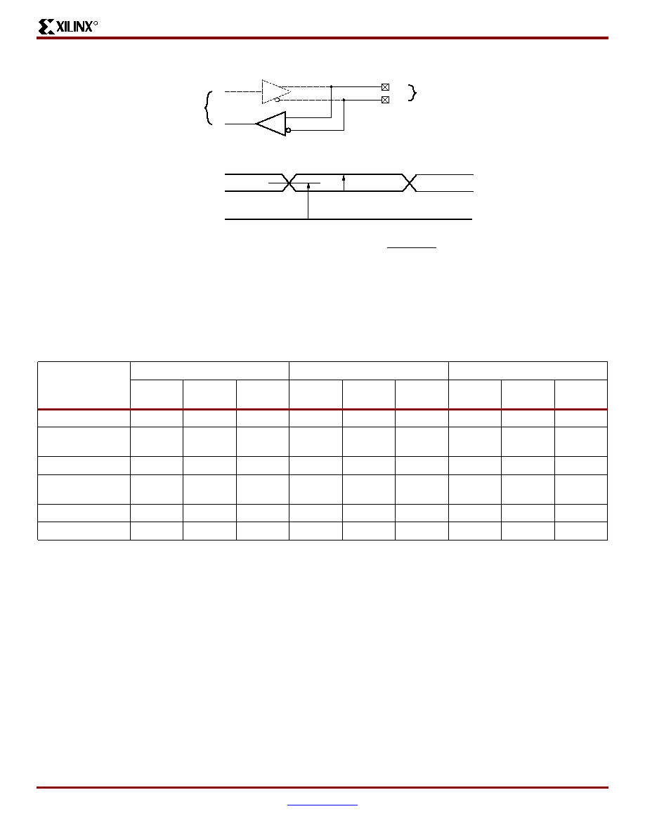
Spartan-3 1.2V FPGA Family: DC and Switching Characteristics
DS099-3 (v1.1) July 11, 2003
www.xilinx.com
7
Advance Product Specification
1-800-255-7778
14
R
Figure 1: Differential Input Voltages
DS099-3_01_040703
V
INN
V
INP
GND level
50%
V
ICM
V
ICM
= Input common mode voltage =
V
ID
V
INP
Internal
Logic
Differential
I/O Pair Pins
V
INN
N
P
2
V
INP
+ V
INN
V
ID
= Differential input voltage = V
INP
- V
INN
Table 9: Recommended Operating Conditions for User I/Os Using Differential Signal Standards
Signal Standard
V
CCO
V
ID
V
ICM
Min (V)
Nom (V)
Max (V)
Min (mV)
Nom
(mV)
Max (mV)
Min (V)
Nom (V)
Max (V)
LDT_25
2.38
2.50
2.63
200
600
1000
0.44
0.60
0.78
LVDS_25,
LVDS_25_DCI
2.38
2.50
2.63
100
350
600
0.30
1.25
2.20
BLVDS_25
2.38
2.50
2.63
-
350
-
-
1.25
-
LVDSEXT_25,
LVDSEXT_25_DCI
2.38
2.50
2.63
100
540
1000
0.30
1.20
2.20
ULVDS_25
2.38
2.50
2.63
200
600
1000
0.44
0.60
0.78
RSDS_25
2.38
2.50
2.63
100
200
-
-
1.30
-
Notes:
1.
The V
REF
input is not used for any of the differential I/O standards.
2.
Of the parameters shown, only V
CCO
represents a voltage measured with respect to GND. The remaining parameters are differential
measurements. See
Figure 1
for parameter definitions.
Spartan-3 1.2V FPGA Family: DC and Switching Characteristics
8
www.xilinx.com
DS099-3 (v1.1) July 11, 2003
1-800-255-7778
Advance Product Specification
R
Figure 2: Differential Output Voltages
DS099-3_02_033103
V
OUTN
V
OUTP
GND level
50%
V
OCM
V
OCM
V
OD
V
OL
V
OH
V
OUTP
Internal
Logic
V
OUTN
N
P
= Output common mode voltage =
2
V
OUTP
+ V
OUTN
V
OD
= Output differential voltage =
V
OH
= Output voltage indicating a High logic level
V
OL
= Output voltage indicating a Low logic level
V
OUTP
- V
OUTN
Differential
I/O Pair Pins
Table 10: DC Characteristics of User I/Os Using Differential Signal Standards
Signal Standard
V
OD
V
OD
V
OCM
V
OCM
V
OH
V
OL
Min
(mV)
Typ
(mV)
Max
(mV)
Min
(mV)
Max
(mV)
Min
(V)
Typ
(V)
Max
(V)
Min
(mV)
Max
(mV)
Typ
(V)
Max
(V)
Min
(V)
Typ
(V)
LDT_25
430
600
670
�15
15
0.495
0.600
0.715
-15
15
-
-
-
-
LVDS_25,
LVDS_25_DCI
250
325
400
-
-
1.125
1.20
1.375
-
-
-
1.475
0.925
-
BLVDS_25
250
350
450
-
-
-
1.20
-
-
-
-
-
-
-
LVDSEXT_25,
LVDSEXT_25_DCI
330
540
700
-
-
1.125
1.20
1.375
-
-
-
1.700
0.705
-
ULVDS_25
430
600
670
-
-
0.495
0.600
0.715
-
-
-
-
-
-
RSDS_25
100
325
400
-
-
1.1
1.2
1.5
-
-
-
-
-
-
Notes:
1.
Of the parameters shown, only V
OH
, V
OL
, and V
OCM
represent voltages measured with respect to GND. The remaining parameters are differential
measurements. See
Figure 2
for parameter definitions.
2.
Output voltage measurements for all differential standards are made with a termination resistor (R
T
) of 100
across the N and P pins of the
differential signal pair.
3.
The numbers in this table are guaranteed over the conditions set forth in
Table 4
and
Table 9
.
Spartan-3 1.2V FPGA Family: DC and Switching Characteristics
DS099-3 (v1.1) July 11, 2003
www.xilinx.com
9
Advance Product Specification
1-800-255-7778
14
R
Switching Characteristics
All Spartan-3 devices are available in two speed grades: �4
and �5. Switching characteristics in this document may be
designated as Advance, Preliminary, or Production. Each
category is defined as follows:
Advance: These speed files are based on simulations only
and are typically available soon after establishing FPGA
specifications. Although speed grades with this designation
are considered relatively stable and conservative, some
under-reporting might still occur.
Preliminary: These speed files are based on complete ES
(engineering sample) silicon characterization. Devices and
speed grades with this designation are intended to give a
better indication of the expected performance of production
silicon. The probability of under-reporting preliminary
delays is greatly reduced compared to Advance data.
Production: These speed files are released once enough
production silicon of a particular device family member has
been characterized to provide full correlation between
speed files and devices over numerous production lots.
There is no under-reporting of delays, and customers
receive formal notification of any subsequent changes. Typ-
ically, the slowest speed grades transition to Production
before faster speed grades.
All specifications are representative of worst-case supply
voltage and junction temperature conditions. Unless other-
wise noted, values apply to all Spartan-3 devices.
Internal timing parameters are derived from measuring
internal test patterns. Timing parameters and their repre-
sentative values are selected for inclusion below either
because they are important as general design requirements
or they indicate fundamental device performance character-
istics. For more complete, more precise, and worst-case
guaranteed data, use the values reported by the Xilinx static
timing analyzer (TRACE in the Xilinx development software)
and back-annotate to the simulation net list.
Table 11: DLL Timing
Symbol
Description
Frequency
Mode
Speed Grade
Units
-5
-4
Min
Max
Min
Max
Clock Outputs
F
1XCO
Frequency at the CLK0 and
CLK180 pins
High
48
326
MHZ
Low
25
180
MHz
Clock Inputs
F
CLKIN
Frequency at the CLKIN pin
High
48
326
MHz
Low
25
180
MHz
T
CLKINJ
Allowable cycle-to-cycle
jitter at the CLKIN pin
High
�100
+100
ps
Low
ps
Notes:
1.
For up-to-date information on DCM timing, see
http://www.xilinx.com/bvdocs/publications/ds099-3.pdf
.
Spartan-3 1.2V FPGA Family: DC and Switching Characteristics
10
www.xilinx.com
DS099-3 (v1.1) July 11, 2003
1-800-255-7778
Advance Product Specification
R
Figure 3: Waveforms for Power-On and the Beginning of Configuration
V
CCINT
(Supply)
(Supply)
(Supply)
V
CCAUX
V
CCO
Bank 4
PROG_B
(Output)
(Open-Drain)
(Input)
INIT_B
CCLK
DS099-3_03_041103
1.2V
2.5V
2.5V
T
ICCK
T
PROG
T
PL
T
POR
Notes:
1.
The V
CCINT
, V
CCAUX
, and V
CCO
supplies may be applied in any order.
2.
The Low-going pulse on PROG_B is optional after power-on but necessary for reconfiguration without a power cycle.
3.
The rising edge of INIT_B samples the voltage levels applied to the mode pins (M0 - M2).
Table 12: Power-On Timing and the Beginning of Configuration
Symbol
Description
Device
All Speed Grades
Units
Min
Max
T
POR
The time from the application of V
CCINT
,
V
CCAUX
, and V
CCO
Bank 4 supply voltages
(whichever occurs last) to the rising
transition of the INIT_B pin
(1)
XC3S50
-
5
ms
XC3S200
-
5
ms
XC3S400
-
5
ms
XC3S1000
-
5
ms
XC3S1500
-
7
ms
XC3S2000
-
7
ms
XC3S4000
-
7
ms
XC3S5000
-
7
ms
T
PROG
The width of the low-going pulse on the
PROG_B pin
All
0.3
-
�s
T
PL
The time from the rising edge of the
PROG_B pin to the rising transition on the
INIT_B pin
(1)
XC3S50
-
2
ms
XC3S200
-
2
ms
XC3S400
-
2
ms
XC3S1000
-
2
ms
XC3S1500
-
3
ms
XC3S2000
-
3
ms
XC3S4000
-
3
ms
XC3S5000
-
3
ms
T
ICCK
The time from the rising edge of the INIT_B
pin to the generation of the configuration
clock signal at the CCLK output pin
(2)
All
0.5
4.0
�s
Notes:
1.
Power-on reset and the clearing of configuration memory occurs during this period.
2.
This specification applies only for the Master Serial and Master Parallel modes.
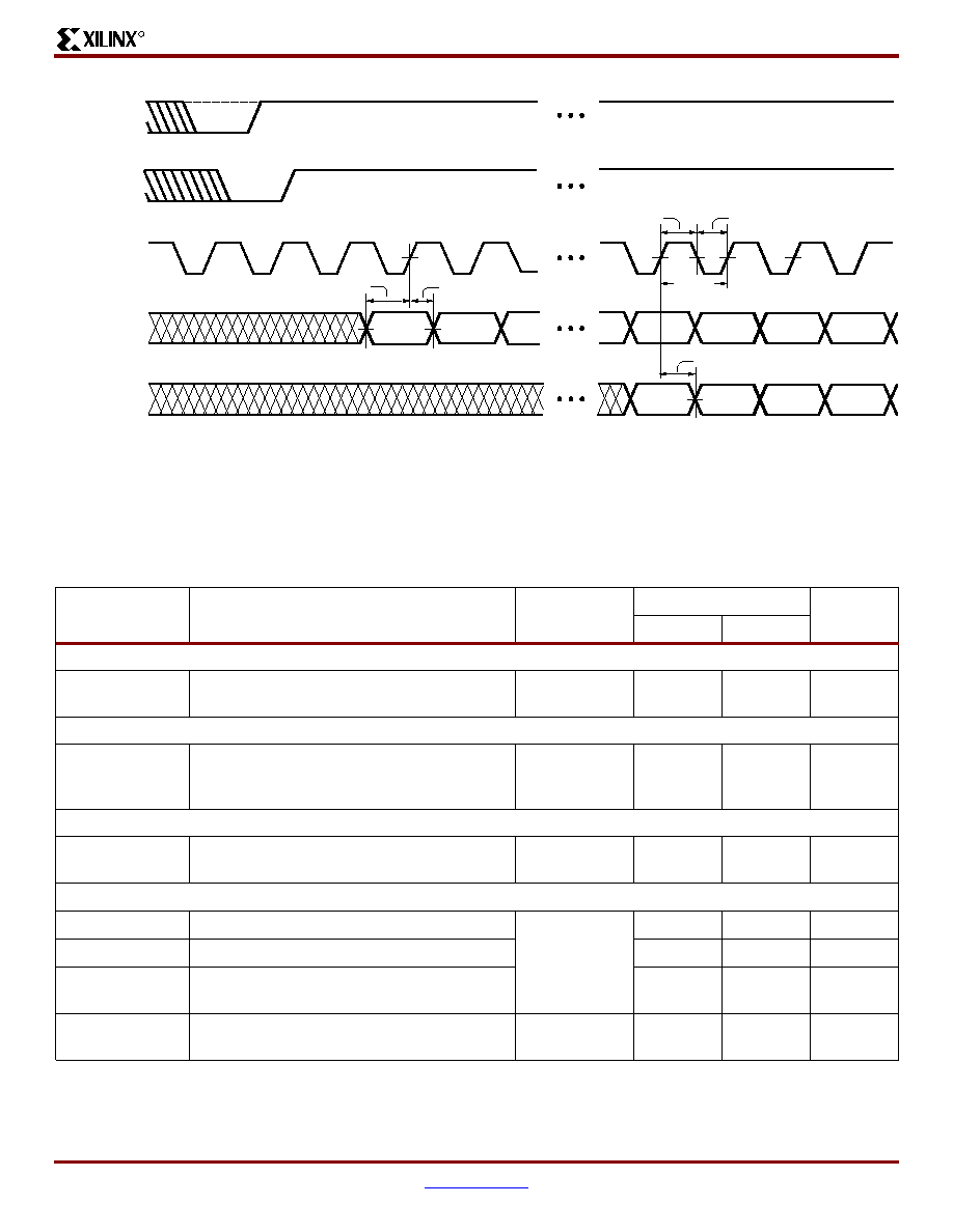
Spartan-3 1.2V FPGA Family: DC and Switching Characteristics
DS099-3 (v1.1) July 11, 2003
www.xilinx.com
11
Advance Product Specification
1-800-255-7778
14
R
Figure 4: Waveforms for Master and Slave Serial Configuration
DS099-3_04_041103
Bit 0
Bit 1
Bit n
Bit n+1
Bit n-64
Bit n-63
1/F
CCSER
T
CCH
T
DCC
T
CCD
T
CCL
T
CCO
PROG_B
(Input)
DIN
(Input)
DOUT
(Output)
(Open-Drain)
INIT_B
(Input/Output)
CCLK
Notes:
1.
The CS_B, WRITE_B, and BUSY signals are not used in the serial modes. Keep the CS_B and WRITE_B inputs inactive (i.e., both
pins High).
Table 13: Timing for the Master and Slave Serial Configuration Modes
Symbol
Description
Slave/Master
All Speed Grades
Units
Min
Max
Setup Times
T
DCC
The time from the setup of data at the DIN pin
to the rising transition at the CCLK pin
Both
-
5.0
ns
Hold Times
T
CCD
The time from the rising transition at the
CCLK pin to the point when data is last held
at the DIN pin
Both
-
0
ns
Clock-to-Output Times
T
CCO
The time from the rising transition on the
CCLK pin to data appearing at the DOUT pin
Both
-
12.0
ns
Clock Timing
T
CCH
The High pulse width at the CCLK input pin
Slave
5.0
-
ns
T
CCL
The Low pulse width at the CCLK input pin
5.0
-
ns
F
CCSER
Frequency of the clock signal at the CCLK
input pin
-
66
MHz
F
CCSER
Variation from the generated CCLK frequency
set using the ConfigRate BitGen option
Master
�50%
+50%
-
Spartan-3 1.2V FPGA Family: DC and Switching Characteristics
12
www.xilinx.com
DS099-3 (v1.1) July 11, 2003
1-800-255-7778
Advance Product Specification
R
Figure 5: Waveforms for Master and Slave Parallel Configuration
DS099-3_05_041103
Byte 0
Byte 1
Byte n
BUSY
High-Z
High-Z
Byte n+1
T
SMWCC
1/F
CCPAR
T
SMCCCS
T
CCL
T
SMCKBY
T
SMCKBY
T
CCH
T
SMCCW
T
SMCCD
T
SMCSCC
T
SMDCC
PROG_B
(Input)
(Open-Drain)
INIT_B
(Input)
CS_B
(Output)
BUSY
RDWR_B
(Input)
(Input/Output)
CCLK
(Inputs)
D0 - D7
Notes:
1.
In a given CCLK cycle, when RDWR_B transitions High or Low while holding CS_B Low, the next rising edge on the CCLK pin will
abort configuration.
Table 14: Timing for the Master and Slave Parallel Configuration Modes
Symbol
Description
Slave/Master
All Speed Grades
Units
Min
Max
Setup Times
T
SMDCC
The time from the setup of data at the D0-D7 pins to the
rising transition at the CCLK pin
Both
5.0
-
ns
T
SMCSCC
The time from the setup of a logic level at the CS_B pin to
the rising transition at the CCLK pin
7.0
-
ns
T
SMCCW
The time from the setup of a logic level at the RDWR_B pin
to the rising transition at the CCLK pin
(1)
7.0
-
ns
Hold Times
T
SMCCD
The time from the rising transition at the CCLK pin to the
point when data is last held at the D0-D7 pins
Both
0
-
ns
T
SMCCCS
The time from the rising transition at the CCLK pin to the
point when a logic level is last held at the CS_B pin
0
-
ns
T
SMWCC
The time from the rising transition at the CCLK pin
(1)
to the
point when a logic level is last held at the RDWR_B pin
(1)
0
-
ns

Spartan-3 1.2V FPGA Family: DC and Switching Characteristics
DS099-3 (v1.1) July 11, 2003
www.xilinx.com
13
Advance Product Specification
1-800-255-7778
14
R
Clock-to-Output Times
T
SMCKBY
The time from the rising transition on the CCLK pin to a
signal transition at the BUSY pin
Slave
-
12.0
ns
Clock Timing
T
CCH
The High pulse width at the CCLK input pin
Slave
5
-
ns
T
CCL
The Low pulse width at the CCLK input pin
5
-
ns
F
CCPAR
Frequency of the clock signal
at the CCLK input pin
Not using the BUSY pin
(2)
-
66
MHz
Using the BUSY pin
-
100
MHz
F
CCPAR
Variation from the generated CCLK frequency set using
the BitGen option ConfigRate
Master
�50%
+50%
-
Notes:
1.
RDWR_B is synchronized to CCLK for the purpose of performing the Abort operation. The same pin asynchronously controls the
driver impedance of the D0 - D7 pins. To avoid contention when writing configuration data to the D0 - D7 bus, do not bring RDWR_B
High when CS_B is Low.
2.
In the Slave Parallel mode, it is necessary to use the BUSY pin when the CCLK frequency exceeds this maximum specification.
Table 14: Timing for the Master and Slave Parallel Configuration Modes (Continued)
Symbol
Description
Slave/Master
All Speed Grades
Units
Min
Max
Figure 6: JTAG Waveforms
TCK
T
TMSTCK
TMS
TDI
TDO
(Input)
(Input)
(Input)
(Output)
T
TCKTMS
T
TCKTDI
T
TCKTDO
T
TDITCK
DS099_06_040703
T
CCH
T
CCL
1/F
TCK
Table 15: Timing for the JTAG Port
Symbol
Description
All Speed Grades
Units
Min
Max
Setup Times
T
TDITCK
The time from the setup of data at the TDI pin to the
rising transition at the TCK pin
4.0
-
ns
T
TMSTCK
The time from the setup of a logic level at the TMS pin
to the rising transition at the TCK pin
4.0
-
ns
Hold Times
T
TCKTDI
The time from the rising transition at the TCK pin to
the point when data is last held at the TDI pin
0
-
ns
Spartan-3 1.2V FPGA Family: DC and Switching Characteristics
14
www.xilinx.com
DS099-3 (v1.1) July 11, 2003
1-800-255-7778
Advance Product Specification
R
Revision History
The Spartan-3 Family Data Sheet
DS099-1, Spartan-3 1.2V FPGA Family:
Introduction and Ordering Information
(Module 1)
DS099-2, Spartan-3 1.2V FPGA Family:
Functional Description
(Module 2)
DS099-3, Spartan-3 1.2V FPGA Family: DC and Switching Characteristics (Module 3)
DS099-4, Spartan-3 1.2V FPGA Family:
Pinout Descriptions
(Module 4)
T
TCKTMS
The time from the rising transition at the TCK pin to
the point when a logic level is last held at the TMS pin
0
-
ns
Clock-to-Output Times
T
TCKTDO
The time from the falling transition on the TCK pin to
data appearing at the TDO pin
-
11.0
ns
Clock Timing
T
CCH
The High pulse width at the TCK pin
5.0
-
ns
T
CCL
The Low pulse width at the TCK pin
5.0
-
ns
F
TCK
Frequency of the clock signal at the TCK pin
-
33
MHz
Date
Version No.
Description
04/11/03
1.0
Initial Xilinx release.
07/11/03
1.1
Extended Absolute Maximum Rating for junction temperature in
Table 1
. Added numbers for
typical quiescent supply current (
Table 6
) and DLL timing (
Table 11
) .
Table 15: Timing for the JTAG Port (Continued)
Symbol
Description
All Speed Grades
Units
Min
Max
DS099-4 (v1.2.2) October 9, 2003
www.xilinx.com
1
Advance Product Specification
1-800-255-7778
� 2003 Xilinx, Inc. All rights reserved. All Xilinx trademarks, registered trademarks, patents, and disclaimers are as listed at
http://www.xilinx.com/legal.htm
.
All other trademarks and registered trademarks are the property of their respective owners. All specifications are subject to change without notice.
Introduction
This data sheet module describes the various pins on a
SpartanTM-3 FPGA and how they connect to the supported
component packages.
�
The
Pin Types
section categorizes all of the FPGA
pins by their function type.
�
The
Pin Definitions
section provides a top-level
description for each pin on the device.
�
The
Detailed, Functional Pin Descriptions
section
offers significantly more detail about each pin,
especially for the dual- or special-function pins used
during device configuration.
�
Some pins have associated optional behavior,
controlled by settings in the configuration bitstream.
These options are described in the
Bitstream Options
section.
�
The
Package Overview
section describes the various
packaging options available for Spartan-3 FPGAs.
Detailed pin list tables and footprint diagrams are
provided for each package solution.
Pin Descriptions
Pin Types
A majority of the pins on a Spartan-3 FPGA are gen-
eral-purpose, user-defined I/O pins. There are, however, up
to 12 different functional types of pins on Spartan-3 pack-
ages, as outlined in
Table 1
. In the package footprint draw-
ings that follow, the individual pins are color-coded
according to pin type as in the table.
098
Spartan-3 1.2V FPGA Family:
Pinout Descriptions
DS099-4 (v1.2.2) October 9, 2003
0
0
Advance Product Specification
R
Table 1: Types of Pins on Spartan-3 FPGAs
Type/
Color
Code
Description
Pin Name(s) in Type
I/O
Unrestricted, general-purpose user-I/O pin. Most pins can be
paired together to form differential I/Os.
IO,
IO_Lxxy_#
DUAL
Dual-purpose pin used in some configuration modes during the
configuration process and then usually available as a user I/O
after configuration. If the pin is not used during configuration, this
pin behaves as an I/O-type pin. There are 12 dual-purpose
configuration pins on every package.
IO_Lxxy_#/DIN/D0, IO_Lxxy_#/D1,
IO_Lxxy_#/D2, IO_Lxxy_#/D3,
IO_Lxxy_#/D4, IO_Lxxy_#/D5,
IO_Lxxy_#/D6, IO_Lxxy_#/D7,
IO_Lxxy_#/CS_B, IO_Lxxy_#/RDWR_B,
IO_Lxxy_#/BUSY/DOUT,
IO_Lxxy_#/INIT_B
CONFIG
Dedicated configuration pin. Not available as a user-I/O pin.
Every package has seven dedicated configuration pins. These
pins are powered by VCCAUX.
CCLK, DONE, M2, M1, M0, PROG_B,
HSWAP_EN
JTAG
Dedicated JTAG pin. Not available as a user-I/O pin. Every
package has four dedicated JTAG pins. These pins are powered
by VCCAUX.
TDI, TMS, TCK, TDO
DCI
Dual-purpose pin that is either a user-I/O pin or used to calibrate
output buffer impedance for a specific bank using Digital
Controlled Impedance (DCI). There are two DCI pins per I/O
bank.
IO/VRN_#
IO_Lxxy_#/VRN_#
IO/VRP_#
IO_Lxxy_#/VRP_#
VREF
Dual-purpose pin that is either a user-I/O pin or, along with all
other VREF pins in the same bank, provides a reference voltage
input for certain I/O standards. If used for a reference voltage
within a bank, all VREF pins within the bank must be connected.
IO/VREF_#
IO_Lxxy_#/VREF_#

Spartan-3 1.2V FPGA Family: Pinout Descriptions
2
www.xilinx.com
DS099-4 (v1.2.2) October 9, 2003
1-800-255-7778
Advance Product Specification
R
I/Os with Lxxy_# are part of a differential output pair. `L' indi-
cates differential output capability. The "xx" field is a
two-digit integer, unique to each bank that identifies a differ-
ential pin-pair. The `y' field is either `P' for the true signal or
`N' for the inverted signal in the differential pair. The `#' field
is the I/O bank number.
Pin Definitions
Table 2
provides a brief description of each pin listed in the
Spartan-3 pinout tables and package footprint diagrams.
Pins are categorized by their pin type, as listed in
Table 1
.
See
Detailed, Functional Pin Descriptions
for more infor-
mation.
GND
Dedicated ground pin. The number of GND pins depends on the
package used. All must be connected.
GND
VCCAUX
Dedicated auxiliary power supply pin. The number of VCCAUX
pins depends on the package used. All must be connected to
+2.5V.
VCCAUX
VCCINT
Dedicated internal core logic power supply pin. The number of
VCCINT pins depends on the package used. All must be
connected to +1.2V.
VCCINT
VCCO
Dedicated I/O bank, output buffer power supply pin. Along with
other VCCO pins in the same bank, this pin supplies power to the
output buffers within the I/O bank and sets the input threshold
voltage for some I/O standards.
VCCO_#
TQ144 Package Only:
VCCO_LEFT, VCCO_TOP,
VCCO_RIGHT, VCCO_BOTTOM
GCLK
Dual-purpose pin that is either a user-I/O pin or an input to a
specific global buffer input. Every package has eight dedicated
GCLK pins.
IO_Lxxy_#/GCLK0, IO_Lxxy_#/GCLK1,
IO_Lxxy_#/GCLK2, IO_Lxxy_#/GCLK3,
IO_Lxxy_#/GCLK4, IO_Lxxy_#/GCLK5,
IO_Lxxy_#/GCLK6, IO_Lxxy_#/GCLK7
N.C.
This package pin is not connected in this specific
device/package combination but may be connected in larger
devices in the same package.
N.C.
Notes:
1.
# = I/O bank number, an integer between 0 and 7.
Table 1: Types of Pins on Spartan-3 FPGAs (Continued)
Type/
Color
Code
Description
Pin Name(s) in Type
Spartan-3 1.2V FPGA Family: Pinout Descriptions
DS099-4 (v1.2.2) October 9, 2003
www.xilinx.com
3
Advance Product Specification
1-800-255-7778
R
Table 2: Spartan-3 Pin Definitions
Pin Name
Direction
Description
I/O: General-purpose I/O pins
I/O
User-defined as input,
output, bidirectional,
three-state output,
open-drain output,
open-source output
User I/O:
Unrestricted single-ended user-I/O pin. Supports all I/O standards
except the differential standards.
I/O_Lxxy_#
User-defined as input,
output, bidirectional,
three-state output,
open-drain output,
open-source output
User I/O, Half of Differential Pair:
Unrestricted single-ended user-I/O pin or half of a differential pair.
Supports all I/O standards including the differential standards.
DUAL: Dual-purpose configuration pins
IO_Lxxy_#/DIN/D0,
IO_Lxxy_#/D1,
IO_Lxxy_#/D2,
IO_Lxxy_#/D3,
IO_Lxxy_#/D4,
IO_Lxxy_#/D5,
IO_Lxxy_#/D6,
IO_Lxxy_#/D7
Input during configuration
Possible bidirectional I/O
after configuration if
SelectMap port is retained.
Otherwise, user I/O after
configuration
Configuration Data Port:
In Parallel (SelectMAP) modes, D0-D7 are byte-wide configuration
data pins. These pins become user I/Os after configuration unless
the SelectMAP port is retained via the Persist bitstream option.
In Serial modes, DIN (D0) serves as the single configuration data
input. This pin becomes a user I/O after configuration unless
retained by the Persist bitstream option.
IO_Lxxy_#/CS_B
Input during Parallel mode
configuration
Possible input after
configuration if SelectMap
port is retained.
Otherwise, user I/O after
configuration
Chip Select for Parallel Mode Configuration:
In Parallel (SelectMAP) modes, this is the active-Low Chip Select
signal. This pin becomes a user I/O after configuration unless the
SelectMAP port is retained via the Persist bitstream option.
IO_Lxxy_#/RDWR_B
Input during Parallel mode
configuration
Possible input after
configuration if SelectMap
port is retained.
Otherwise, user I/O after
configuration
Read/Write Control for Parallel Mode Configuration:
In Parallel (SelectMAP) modes, this is the active-Low Write
Enable, active-High Read Enable signal. This pin becomes a user
I/O after configuration unless the SelectMAP port is retained via
the Persist bitstream option.
IO_Lxxy_#/
BUSY/DOUT
Output during configuration
Possible output after
configuration if SelectMap
port is retained.
Otherwise, user I/O after
configuration
Configuration Data Rate Control for Parallel Mode, Serial Data
Output for Serial Mode:
In Parallel (SelectMAP) modes, BUSY throttles the rate at which
configuration data is loaded. This pin becomes a user I/O after
configuration unless the SelectMAP port is retained via the Persist
bitstream option.
In Serial modes, DOUT provides preamble and configuration data
to downstream devices in a multi-FPGA daisy-chain. This pin
becomes a user I/O after configuration.
Spartan-3 1.2V FPGA Family: Pinout Descriptions
4
www.xilinx.com
DS099-4 (v1.2.2) October 9, 2003
1-800-255-7778
Advance Product Specification
R
IO_Lxxy_#/INIT_B
Bidirectional (open-drain)
during configuration
User I/O after configuration
Initializing Configuration Memory/Detected Configuration Error:
When Low, this pin indicates that configuration memory is being
cleared. When held Low, this pin delays the start of configuration.
After this pin is released or configuration memory is cleared, the
pin goes High. During configuration, a Low on this output indicates
that a configuration data error occurred. This pin becomes a user
I/O after configuration.
DCI: Digitally Controlled Impedance reference resistor input pins
IO_Lxxy_#/VRN_# or
IO/VRN_#
Input when using DCI
Otherwise, same as I/O
DCI Reference Resistor for NMOS I/O Transistor (per bank):
If using DCI, a 1% precision impedance-matching resistor is
connected between this pin and the VCCO supply for this bank.
Otherwise, this pin is a user I/O.
IO_Lxxy_#/VRP_# or
IO/VRP_#
Input when using DCI
Otherwise, same as I/O
DCI Reference Resistor for PMOS I/O Transistor (per bank):
If using DCI, a 1% precision impedance-matching resistor is
connected between this pin and the ground supply. Otherwise, this
pin is a user I/O.
GCLK: Global clock buffer inputs
IO_Lxxy_#/GCLK0,
IO_Lxxy_#/GCLK1,
IO_Lxxy_#/GCLK2,
IO_Lxxy_#/GCLK3,
IO_Lxxy_#/GCLK4,
IO_Lxxy_#/GCLK5,
IO_Lxxy_#/GCLK6,
IO_Lxxy_#/GCLK7
Input if connected to global
clock buffers
Otherwise, same as I/O
Global Buffer Input:
Direct input to a low-skew global clock buffer. If not connected to a
global clock buffer, this pin is a user I/O.
VREF: I/O bank input reference voltage pins
IO_Lxxy_#/VREF_#
or
IO/VREF_#
Voltage supply input when
VREF pins are used within a
bank.
Otherwise, same as I/O
Input Buffer Reference Voltage for Special I/O Standards (per
bank):
If required to support special I/O standards, all the VREF pins
within a bank connect to a input threshold voltage source.
If not used as input reference voltage pins, these pins are available
as individual user-I/O pins.
CONFIG: Dedicated configuration pins
CCLK
Input in Slave configuration
modes
Output in Master
configuration modes
Configuration Clock:
The configuration clock signal synchronizes configuration data.
PROG_B
Input
Program/Configure Device:
Active Low asynchronous reset to configuration logic. Asserting
PROG_B Low for an extended period delays the configuration
process. This pin has an internal weak pull-up resistor during
configuration.
Table 2: Spartan-3 Pin Definitions (Continued)
Pin Name
Direction
Description
Spartan-3 1.2V FPGA Family: Pinout Descriptions
DS099-4 (v1.2.2) October 9, 2003
www.xilinx.com
5
Advance Product Specification
1-800-255-7778
R
DONE
Bidirectional with open-drain
or totem-pole Output
Configuration Done, Delay Start-up Sequence:
A Low-to-High output transition on this bidirectional pin signals the
end of the configuration process.
The FPGA produces a Low-to-High transition on this pin to
indicate that the configuration process is complete. The DriveDone
bitstream generation option defines whether this pin functions as
a totem-pole output that actively drives High or as an open-drain
output. An open-drain output requires a pull-up resistor to produce
a High logic level. The open-drain option permits the DONE lines
of multiple FPGAs to be tied together, so that the common node
transitions High only after all of the FPGAs have completed
configuration. Externally holding the open-drain output Low delays
the start-up sequence, which marks the transition to user mode.
M0, M1, M2
Input
Configuration Mode Selection:
These inputs select the configuration mode. The logic levels
applied to the mode pins are sampled on the rising edge of INIT_B.
See
Table 7
.
HSWAP_EN
Input
Disable Weak Pull-up Resistors During Configuration:
A Low on this pin enables weak pull-up resistors on all pins that are
not actively involved in the configuration process. A High value
disables all pull-ups, allowing the non-configuration pins to float.
JTAG: JTAG interface pins
TCK
Input
JTAG Test Clock:
The TCK clock signal synchronizes all JTAG port operations.
TDI
Input
JTAG Test Data Input:
TDI is the serial data input for all JTAG instruction and data
registers.
TMS
Input
JTAG Test Mode Select:
The serial TMS input controls the operation of the JTAG port.
TDO
Output
JTAG Test Data Output:
TDO is the serial data output for all JTAG instruction and data
registers.
VCCO: I/O bank output voltage supply pins
VCCO_#
Supply
Power Supply for Output Buffer Drivers (per bank):
These pins power the output drivers within a specific I/O bank.
VCCAUX: Auxiliary voltage supply pins
VCCAUX
Supply
Power Supply for Auxiliary Circuits:
+2.5V power pins for auxiliary circuits, including the Digital Clock
Managers (DCMs), the dedicated configuration pins (CONFIG),
and the dedicated JTAG pins. All VCCAUX pins must be
connected.
VCCINT: Internal core voltage supply pins
VCCINT
Supply
Power Supply for Internal Core Logic:
+1.2V power pins for the internal logic. All pins must be connected.
Table 2: Spartan-3 Pin Definitions (Continued)
Pin Name
Direction
Description
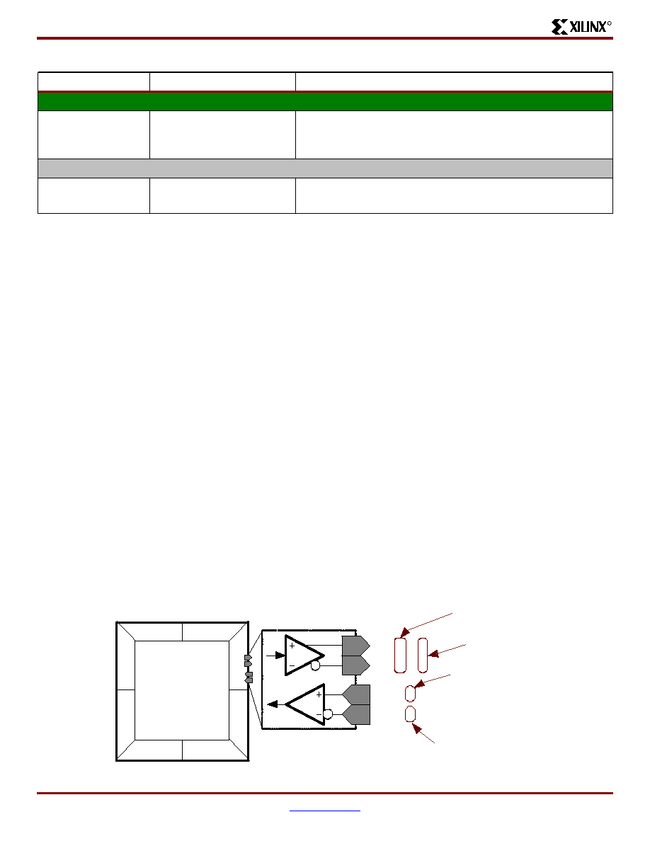
Spartan-3 1.2V FPGA Family: Pinout Descriptions
6
www.xilinx.com
DS099-4 (v1.2.2) October 9, 2003
1-800-255-7778
Advance Product Specification
R
Detailed, Functional Pin Descriptions
I/O Type: Unrestricted, General-purpose I/O
Pins
After configuration, I/O-type pins are inputs, outputs, bidi-
rectional I/O, three-state outputs, open-drain outputs, or
open-source outputs, as defined in the application
Pins labeled "IO" support all SelectIOTM signal standards
except differential standards. A given device at most only
has a few of these pins.
A majority of the general-purpose I/O pins are labeled in the
format "IO_Lxxy_#". These pins support all SelectIO signal
standards, including the differential standards such as
LVDS, ULVDS, BLVDS, RSDS, or LDT.
For additional information, see the "
IOBs
" section in Module
2:
Functional Description
.
Differential Pair Labeling
A pin supports differential standards if the pin is labeled in
the format "Lxxy_#". The pin name suffix has the following
significance.
Figure 1
provides a specific example showing
a differential input to and a differential output from Bank 2.
�
`L' indicates differential capability.
�
"xx" is a two-digit integer, unique for each bank, that
identifies a differential pin-pair.
�
`y' is replaced by `P' for the true signal or `N' for the
inverted. These two pins form one differential pin-pair.
�
`#' is an integer, 0 through 7, indicating the associated
I/O bank.
If unused, these pins are in a high impedance state. The Bit-
stream generator option UnusedPin enables a weak pull-up
or pull-down resistor on all unused I/O pins.
Behavior from Power-On through End of Configu-
ration
During the configuration process, all pins that are not
actively involved in the configuration process are in a
high-impedance state. The HSWAP_EN input determines
whether or not weak pull-up resistors are enabled during
configuration. HSWAP_EN = 0 enables the weak pull-up
resistors. HSWAP_EN = 1 disables the pull-up resistors
allowing the pins to float, which is the desired state for
hot-swap applications.
GND: Ground supply pins
GND
Supply
Ground:
Ground pins, which are connected to the power supply's return
path. All pins must be connected.
N.C.: Unconnected package pins
N.C.
Unconnected Package Pin:
These package pins are unconnected.
Notes:
1.
All unused inputs and bidirectional pins must be tied either High or Low. For unused enable inputs, apply the level that disables the
associated function. One common approach is to activate internal pull-up or pull-down resistors. An alternative approach is to
externally connect the pin to either VCCO or GND.
2.
All outputs are of the totem-pole type -- i.e., they can drive High as well as Low logic levels -- except for the cases where "Open
Drain" is indicated. The latter can only drive a Low logic level and require a pull-up resistor to produce a High logic level.
Table 2: Spartan-3 Pin Definitions (Continued)
Pin Name
Direction
Description
Figure 1: Differential Pair Labelling
IO_L38P_2
IO_L38N_2
IO_L39P_2
IO_L39N_2
Bank 0
Bank 1
Bank 4
Bank 5
Ba
n
k
2
Ba
n
k
3
Ba
n
k
6
B
a
n
k
7
Pair Number
Bank Number
Positive Polarity,
True Driver
Negative Polarity,
Inverted Driver
DS099-4_01_042303

Spartan-3 1.2V FPGA Family: Pinout Descriptions
DS099-4 (v1.2.2) October 9, 2003
www.xilinx.com
7
Advance Product Specification
1-800-255-7778
R
DUAL Type: Dual-Purpose Configuration and
I/O Pins
These pins serve dual purposes. The user-I/O pins are tem-
porarily borrowed during the configuration process to load
configuration data into the FPGA. After configuration, these
pins are then usually available as a user I/O in the applica-
tion. If a pin is not applicable to the specific configuration
mode--controlled by the mode select pins M2, M1, and
M0--then the pin behaves as an I/O-type pin.
There are 12 dual-purpose configuration pins on every
package, six of which are part of I/O Bank 4, the other six
part of I/O Bank 5. Only a few of the pins in Bank 4 are used
in the Serial configuration modes.
See
"
Configuration
" in Module 2:
Functional Description
.
See
"Pin Behavior During Configuration, page 15".
Serial Configuration Modes
This section describes the dual-purpose pins used during
either Master or Slave Serial mode. See
Table 7
for Mode
Select pin settings required for Serial modes. All such pins
are in Bank 4 and powered by VCCO_4.
In both the Master and Slave Serial modes, DIN is the serial
configuration data input. The D1-D7 inputs are unused in
serial mode and behave like general-purpose I/O pins.
In all the cases, the configuration data is synchronized to
the rising edge of the CCLK clock signal.
The DIN, DOUT, and INIT_B pins can be retained in the
application to support reconfiguration by setting the Persist
bitstream generation option. However, the serial modes do
not support device readback.
Table 3: Dual-Purpose Pins Used in Master or Slave Serial Mode
Pin Name
Direction
Description
DIN
Input
Serial Data Input:
During the Master or Slave Serial configuration modes, DIN is the serial configuration data
input, and all data is synchronized to the rising CCLK edge. After configuration, this pin is
available as a user I/O.
This signal is located in Bank 4 and its output voltage determined by VCCO_4.
The BitGen option Persist permits this pin to retain its configuration function in the User
mode.
DOUT
Output
Serial Data Output:
In a multi-FPGA design where all the FPGAs use serial mode, connect the DOUT output of
one FPGA--in either Master or Slave Serial mode--to the DIN input of the next FPGA--in
Slave Serial mode--so that configuration data passes from one to the next, in daisy-chain
fashion. This "daisy chain" permits sequential configuration of multiple FPGAs.
This signal is located in Bank 4 and its output voltage determined by VCCO_4.
The BitGen option Persist permits this pin to retain its configuration function in the User
mode.
INIT_B
Bidirectional
(open-drain)
Initializing Configuration Memory/Configuration Error:
Just after power is applied, the FPGA produces a Low-to-High transition on this pin
indicating that initialization (i.e., clearing) of the configuration memory has finished. Before
entering the User mode, this pin functions as an open-drain output, which requires a pull-up
resistor in order to produce a High logic level. In a multi-FPGA design, tie (wire AND) the
INIT_B pins from all FPGAs together so that the common node transitions High only after
all of the FPGAs have been successfully initialized.
Externally holding this pin Low beyond the initialization phase delays the start of
configuration. This action stalls the FPGA at the configuration step just before the mode
select pins are sampled.
During configuration, the FPGA indicates the occurrence of a data (i.e., CRC) error by
asserting INIT_B Low.
This signal is located in Bank 4 and its output voltage determined by VCCO_4.
The BitGen option Persist permits this pin to retain its configuration function in the User
mode.

Spartan-3 1.2V FPGA Family: Pinout Descriptions
8
www.xilinx.com
DS099-4 (v1.2.2) October 9, 2003
1-800-255-7778
Advance Product Specification
R
Parallel Configuration Modes (SelectMAP)
This section describes the dual-purpose configuration pins
used during the Master and Slave Parallel configuration
modes, sometimes also called the SelectMAP modes. In
both Master and Slave Parallel configuration modes, D0-D7
form the byte-wide configuration data input. See
Table 7
for
Mode Select pin settings required for Parallel modes.
As shown in
Figure 2
, D0 is the most-significant bit while D7
is the least-significant bit. Bits D0-D3 form the high nibble of
the byte and bits D4-D7 form the low nibble.
In the Parallel configuration modes, both the VCCO_4 and
VCCO_5 voltage supplies are required and must both equal
the voltage of the attached configuration device, typically
either 2.5V or 3.3V.
Assert Low both the chip-select pin, CS_B, and the
read/write control pin, RDWR_B, to write the configuration
data byte presented on the D0-D7 pins to the FPGA on a
rising-edge of the configuration clock, CCLK. The order of
CS_B and RDWR_B does not matter, although RDWR_B
must be asserted throughout the configuration process. If
RDWR_B is de-asserted during configuration, the FPGA
aborts the configuration operation.
After configuration, these pins are available as general-pur-
pose user I/O. However, the SelectMAP configuration inter-
face is optionally available for debugging and dynamic
reconfiguration. To use these SelectMAP pins after configu-
ration, set the Persist bitstream generation option.
The Readback debugging option, for example, requires the
Persist bitstream generation option. During Readback
mode, assert CS_B Low, along with RDWR_B High, to read
a configuration data byte from the FPGA to the D0-D7 bus
on a rising CCLK edge. During Readback mode, D0-D7 are
output pins.
In all the cases, the configuration data and control signals
are synchronized to the rising edge of the CCLK clock sig-
nal.
I/O Bank 4 (VCCO_4)
I/O Bank 5 (VCCO_5)
High Nibble
Low Nibble
Configuration Data Byte
D0
D1
D2
D3
D4
D5
D6
D7
0xA5 =
1
0
1
0
0
1
0
1
Figure 2: Configuration Data Byte Mapping to D0-D7 Bits
Spartan-3 1.2V FPGA Family: Pinout Descriptions
DS099-4 (v1.2.2) October 9, 2003
www.xilinx.com
9
Advance Product Specification
1-800-255-7778
R
Table 4: Dual-Purpose Configuration Pins for Parallel (SelectMAP) Configuration Modes
Pin
Name
Direction
Description
D0,
D1,
D2,
D3
Input during
configuration
Output during
readback
Configuration Data Port (high nibble):
Collectively, the D0-D7 pins are the byte-wide configuration data port for the Parallel
(SelectMAP) configuration modes. Configuration data is synchronized to the rising edge of
CCLK clock signal.
The D0-D3 pins are the high nibble of the configuration data byte and located in Bank 4 and
powered by VCCO_4.
The BitGen option Persist permits this pin to retain its configuration function in the User mode.
D4,
D5,
D6,
D7
Input during
configuration
Output during
readback
Configuration Data Port (low nibble):
The D4-D7 pins are the low nibble of the configuration data byte. However, these signals are
located in Bank 5 and powered by VCCO_5.
The BitGen option Persist permits this pin to retain its configuration function in the User mode.
CS_B
Input
Chip Select for Parallel Mode Configuration:
Assert this pin Low, together with RDWR_B to write a configuration data byte from the D0-D7
bus to the FPGA on a rising CCLK edge.
During Readback, assert this pin Low, along with RDWR_B High, to read a configuration data
byte from the FPGA to the D0-D7 bus on a rising CCLK edge.
This signal is located in Bank 5 and powered by VCCO_5.
The BitGen option Persist permits this pin to retain its configuration function in the User mode.
CS_B
Function
0
FPGA selected. SelectMAP inputs are valid on the next rising edge of CCLK.
1
FPGA deselected. All SelectMAP inputs are ignored.
Spartan-3 1.2V FPGA Family: Pinout Descriptions
10
www.xilinx.com
DS099-4 (v1.2.2) October 9, 2003
1-800-255-7778
Advance Product Specification
R
JTAG Configuration Mode
In the JTAG configuration mode all dual-purpose configura-
tion pins are unused and behave exactly like user-I/O pins,
as shown in
Table 10
. See
Table 7
for Mode Select pin set-
tings required for JTAG mode.
Dual-Purpose Pin I/O Standard During Configura-
tion
During configuration, the dual-purpose pins default to
CMOS input and output levels for the associated VCCO
voltage supply pins. For example, in the Parallel configura-
tion modes, both VCCO_4 and VCCO_5 are required. If
connected to +2.5V, then the associated pins conform to the
LVCMOS25 I/O standard. If connected to +3.3V, then the
pins drive LVCMOS output levels and accept either LVTTL
or LVCMOS input levels.
Dual-Purpose Pin Behavior After Configuration
After the configuration process completes, these pins, if
they were borrowed during configuration, become user-I/O
pins available to the application. If a dual-purpose configu-
ration pin is not used during the configuration process--i.e.,
the parallel configuration pins when using serial
mode--then the pin behaves exactly like a general-purpose
I/O. See
I/O Type: Unrestricted, General-purpose I/O
Pins
section above.
RDWR_B
Input
Read/Write Control for Parallel Mode Configuration:
In Master and Slave Parallel modes, assert this pin Low together with CS_B to write a
configuration data byte from the D0-D7 bus to the FPGA on a rising CCLK edge. Once
asserted during configuration, RDWR_B must remain asserted until configuration is
complete.
During Readback, assert this pin High with CS_B Low to read a configuration data byte from
the FPGA to the D0-D7 bus on a rising CCLK edge.
This signal is located in Bank 5 and powered by VCCO_5.
The BitGen option Persist permits this pin to retain its configuration function in the User mode.
BUSY
Output
Configuration Data Rate Control for Parallel Mode:
In the Slave and Master Parallel modes, BUSY throttles the rate at which configuration data
is loaded. BUSY is only necessary if CCLK operates at greater than 50 MHz. Ignore BUSY
for frequencies of 50 MHz and below.
When BUSY is Low, the FPGA accepts the next configuration data byte on the next rising
CCLK edge for which CS_B and RDWR_B are Low. When BUSY is High, the FPGA ignores
the next configuration data byte. The next configuration data value must be held or reloaded
until the next rising CCLK edge when BUSY is Low. When CS_B is High, BUSY is in a high
impedance state.
This signal is located in Bank 4 and its output voltage is determined by VCCO_4. The BitGen
option Persist permits this pin to retain its configuration function in the User mode.
INIT_B
Bidirectional
(open-drain)
Initializing Configuration Memory/Configuration Error (active-Low):
See description under
Serial Configuration Modes, page 7
.
Table 4: Dual-Purpose Configuration Pins for Parallel (SelectMAP) Configuration Modes (Continued)
Pin
Name
Direction
Description
RDWR_B
Function
0
If CS_B is Low, then load (write) configuration data to the FPGA.
1
This option is valid only if the Persist bitstream option is set to Yes. If CS_B is
Low, then read configuration data from the FPGA.
BUSY
Function
0
The FPGA is ready to accept the next configuration data byte.
1
The FPGA is busy processing the current configuration data byte and is not
ready to accept the next byte.
Hi-Z
If CS_B is High, then BUSY is high impedance.

Spartan-3 1.2V FPGA Family: Pinout Descriptions
DS099-4 (v1.2.2) October 9, 2003
www.xilinx.com
11
Advance Product Specification
1-800-255-7778
R
DCI: User I/O or Digitally Controlled
Impedance Resistor Reference Input
These pins are individual user-I/O pins unless one of the I/O
standards used in the bank requires the Digitally Controlled
Impedance (DCI) feature. If DCI is used, then 1% precision
resistors connected to the VRP_# and VRN_# pins match
the impedance on the input or output buffers of the I/O stan-
dards that use DCI within the bank.
The `#' character in the pin name indicates the associated
I/O bank and is an integer, 0 through 7.
There are two DCI pins per I/O bank, except in the TQ144
package, which does not have any DCI inputs for Bank 5.
VRP and VRN Impedance Resistor Reference
Inputs
The 1% precision impedance-matching resistor attached to
the VRP_# pin controls the pull-up impedance of PMOS
transistor in the input or output buffer. Consequently, the
VRP_# pin must connect to ground. The `P' character in
"VRP" indicates that this pin controls the I/O buffer's PMOS
transistor impedance. The VRP_# pin is used for both single
and split termination.
The 1% precision impedance-matching resistor attached to
the VRN_# pin controls the pull-down impedance of NMOS
transistor in the input or output buffer. Consequently, the
VRN_# pin must connect to VCCO. The `N' character in
"VRN" indicates that this pin controls the I/O buffer's NMOS
transistor impedance. The VRN_# pin is only used for split
termination.
Each VRN or VRP reference input requires its own resistor.
A single resistor cannot be shared between VRN or VRP
pins associated with different banks.
During configuration, these pins behave exactly like
user-I/O pins. The associated DCI behavior is not active or
valid until after configuration completes.
See
"
Digitally Controlled Impedance (DCI)
" in Module 2:
Functional Description
.
DCI Termination Types
If the I/O in an I/O bank do not use the DCI feature, then no
external resistors are required and both the VRP_# and
VRN_# pins are available for user I/O, as shown in
Figure 3a
.
If the I/O standards within the associated I/O bank require
single termination--such as GTL_DCI, GTLP_DCI, or
HSTL_III_DCI--then only the VRP_# signal connects to a
1% precision impedance-matching resistor, as shown in
Figure 3b
. The VRN_# pin is available for user I/O.
Finally, if the I/O standards with the associated I/O bank
require split termination--such as HSTL_I_DCI,
SSTL2_I_DCI, SSTL2_II_DCI, or LVDS_25_DCI and
LVDSEXT_25_DCI receivers--then both the VRP_# and
VRN_# pins connect to separate 1% precision imped-
ance-matching resistors, as shown in
Figure 3c
. Neither pin
is available for user I/O.
GCLK: Global Clock Buffer Inputs or
General-Purpose I/O Pins
These pins are user-I/O pins unless they specifically con-
nect to one of the eight low-skew global clock buffers on the
device, specified using the IBUFG primitive.
There are eight GCLK pins per device and two each appear
in the top-edge banks, Bank 0 and 1, and the bottom-edge
banks, Banks 4 and 5. See
Figure 1
for a picture of bank
labeling.
During configuration, these pins behave exactly like
user-I/O pins.
CONFIG: Dedicated Configuration Pins
The dedicated configuration pins control the configuration
process and are not available as user-I/O pins. Every pack-
age has seven dedicated configuration pins. All CON-
FIG-type pins are powered by the +2.5V VCCAUX supply.
See
"
Configuration
" in Module 2:
Functional Description
.
CCLK: Configuration Clock
The configuration clock signal on this pin synchronizes the
reading or writing of configuration data. This pin is an input
for the Slave configuration modes, both parallel and serial.
After configuration, the CCLK pin is in a high-impedance,
floating state. By default, CCLK optionally is pulled High to
VCCAUX as defined by the CclkPin bitstream selection. Any
clocks applied to CCLK after configuration are ignored
unless the bitstream option Persist is set to Yes, which
retains the configuration interface. Persist is set to No by
default. However, if Persist is set to Yes, then all clock edges
are potentially active events, depending on the other config-
uration control signals.
The bitstream generator option ConfigRate determines the
frequency of the internally-generated CCLK oscillator
required for the Master configuration modes. The actual fre-
quency is approximate due to the characteristics of the sili-
con oscillator and varies by up to 30% over the temperature
and voltage range. By default, CCLK operates at approxi-
mately 6 MHz. Via the ConfigRate option, the oscillator fre-
quency is set at approximately 3, 6, 12, 25, or 50 MHz. At
power-on, CCLK always starts operation at its lowest fre-
quency. The device does not start operating at the higher
frequency until the ConfigRate control bits are loaded dur-
ing the configuration process.
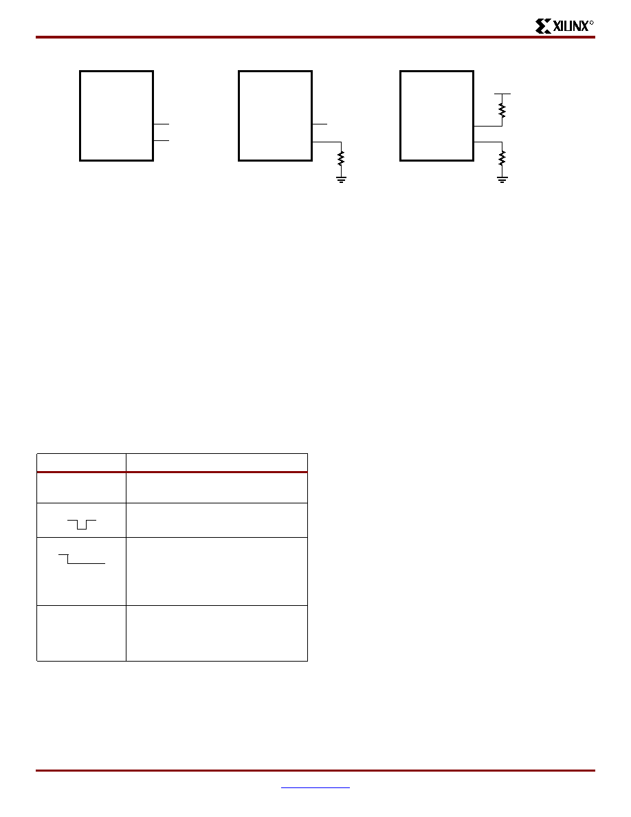
Spartan-3 1.2V FPGA Family: Pinout Descriptions
12
www.xilinx.com
DS099-4 (v1.2.2) October 9, 2003
1-800-255-7778
Advance Product Specification
R
PROG_B: Program/Configure Device
This asynchronous pin initiates the configuration or re-con-
figuration processes. A Low-going pulse resets the configu-
ration logic, initializing the configuration memory. This
initialization process cannot finish until PROG_B returns
High. Asserting PROG_B Low for an extended period
delays the configuration process. At power-up, there is
always a weak pull-up resistor to VCCAUX on this pin. After
configuration, the bitstream generator option ProgPin deter-
mines whether or not the weak pull-up resistor is present.
By default, the ProgPin option retains the weak pull-up
resistor.
After configuration, hold the PROG_B input High. Any
Low-going pulse on PROG_B restarts the configuration pro-
cess.
DONE: Configuration Done, Delay Start-Up
Sequence
The FPGA produces a Low-to-High transition on this pin
indicating that the configuration process is complete. The
bitstream generator option DriveDone determines whether
this pin functions as a totem-pole output that can drive High
or as an open-drain output. If configured as an open-drain
output--which is the default behavior--then a pull-up resis-
tor is required to produce a High logic level. There is a bit-
stream option that provides an internal weak pull-up
resistor, otherwise an external pull-up resistor is required.
The open-drain option permits the DONE lines of multiple
FPGAs to be tied together, so that the common node transi-
tions High only after all of the FPGAs have completed con-
figuration. Externally holding the open-drain DONE pin Low
delays the start-up sequence, which marks the transition to
user mode.
Once the FPGA enters User mode after completing config-
uration, the DONE pin no longer drives the DONE pin Low.
The bitstream generator option DonePin determines
whether or not a weak pull-up resistor is present on the
DONE pin to pull the pin to VCCAUX. If the weak pull-up
resistor is eliminated, then the DONE pin must be pulled
High using an external pull-up resistor or one of the FPGAs
in the design must actively drive the DONE pin High via the
DriveDone bitstream generator option.
The bitstream generator option DriveDone causes the
FPGA to actively drive the DONE output High after configu-
ration. This option should only be used in single-FPGA
designs or on the last FPGA in a multi-FPGA daisy-chain.
By default, the bitstream generator software retains the
weak pull-up resistor and does not actively drive the DONE
pin as highlighted in
Table 6
.
Table 6
shows the interaction
of these bitstream options in single- and multi-FPGA
designs.
Figure 3: DCI Termination Types
DS099-4_03_042203
VCCO
VRN
VRP
One of eight
I/O Banks
R
REF
(1%)
R
REF
(1%)
(c) Split termination
User I/O
VRP
One of eight
I/O Banks
R
REF
(1%)
(b) Single termination
User I/O
User I/O
One of eight
I/O Banks
(a) No termination
Table 5: PROG_B Operation
PROG_B Input
Response
Power-up
Automatically initiates configuration
process.
Low-going pulse
Initiate (re-)configuration process and
continue to completion.
Extended Low
Initiate (re-)configuration process and
stall process at step where
configuration memory is cleared.
Process is stalled until PROG_B
returns High.
1
If the configuration process is started,
continue to completion. If
configuration process is complete,
stay in User mode.
Spartan-3 1.2V FPGA Family: Pinout Descriptions
DS099-4 (v1.2.2) October 9, 2003
www.xilinx.com
13
Advance Product Specification
1-800-255-7778
R
M2, M1, M0: Configuration Mode Selection
These inputs select the mode to configure the FPGA. The
logic levels applied to the mode pins are sampled on the ris-
ing edge of INIT_B.
In user mode, after configuration successfully completes,
any levels applied to these input are ignored. Each of the
bitstream generator options M0Pin, M1Pin, and M2Pin
determines whether a weak pull-up resistor, weak pull-down
resistor, or no resistor is present on its respective mode pin,
M0, M1, or M2.
HSWAP_EN: Disable Weak Pull-up Resistors Dur-
ing Configuration
A Low on this asynchronous pin enables weak pull-up resis-
tors on all user I/Os, although only until device configuration
completes. A High disables the weak pull-up resistors (dur-
ing configuration, which is the desired state for some appli-
cations.
After configuration, HSWAP_EN essentially becomes a
"don't care" input and any pull-up resistors previously
enabled by HSWAP_EN are disabled. If a user I/O in the
application requires a weak pull-up resistor after configura-
tion, place a PULLUP primitive on the associated I/O pin.
The Bitstream generator option HswapenPin determines
whether a weak pull-up resistor to VCCAUX, a weak
pull-down resistor, or no resistor is present on HSWAP_EN
after configuration.
JTAG: Dedicated JTAG Port Pins
These pins are dedicated connections to the four-wire IEEE
1532/IEEE 1149.1 JTAG port, shown in
Figure 4
and
Table 6: DonePin and DriveDone Bitstream Option Interaction
DonePin
DriveDone
Single- or Multi-
FPGA Design
Comments
Pullnone
No
Single
External pull-up resistor, with value between 330
to 3.3k, required on
DONE.
Pullnone
No
Multi
External pull-up resistor, with value between 330
to 3.3k, required on
common node connecting to all DONE pins.
Pullnone
Yes
Single
OK, no external requirements.
Pullnone
Yes
Multi
DriveDone on last device in daisy-chain only. No external requirements.
Pullup
No
Single
OK, but weak pull-up on DONE pin has slow rise time. May require 330
pull-up resistor for high CCLK frequencies.
Pullup
No
Multi
External pull-up resistor, with value between 330
to 3.3k, required on
common node connecting to all DONE pins.
Pullup
Yes
Single
OK, no external requirements.
Pullup
Yes
Multi
DriveDone on last device in daisy-chain only. No external requirements.
Table 7: Spartan-3 Configuration Mode Select Settings
Configuration Mode
M2
M1
M0
Master Serial
0
0
0
Slave Serial
1
1
1
Master Parallel
0
1
1
Slave Parallel
1
1
0
JTAG
1
0
1
Reserved
0
0
1
Reserved
0
1
0
Reserved
1
0
0
After Configuration
X
X
X
Notes:
1.
X = don't care, either 0 or 1.
Table 8: HSWAP_EN Encoding
HSWAP_EN
Function
During Configuration
0
Enable weak pull-up resistors on all pins
not actively involved in the configuration
process. Pull-ups are only active until
configuration completes. See
Table 10
.
1
No pull-up resistors during configuration.
After Configuration, User Mode
X
This pin has no function except during
device configuration.
Notes:
1.
X = don't care, either 0 or 1.

Spartan-3 1.2V FPGA Family: Pinout Descriptions
14
www.xilinx.com
DS099-4 (v1.2.2) October 9, 2003
1-800-255-7778
Advance Product Specification
R
described in
Table 9
. The JTAG port is used for bound-
ary-scan testing, device configuration, application debug-
ging, and possibly an additional serial port for the
application. These pins are dedicated and are not available
as user-I/O pins. Every package has four dedicated JTAG
pins and these pins are powered by the +2.5V VCCAUX
supply.
Using JTAG Port After Configuration
By default, the JTAG port is disabled after the configuration
process completes. To continue using the JTAG port, after
configuration, place a BSCAN_SPARTAN3 primitive in the
design.
Furthermore, the contents of the User ID register within the
JTAG port can be specified as a Bitstream Generation
option. By default, the 32-bit User ID register contains
0xFFFFFFFF.
Precautions When Using the JTAG Port in 3.3V
Environments
The JTAG port is powered by the +2.5V VCCAUX power
supply. The JTAG pins can tolerate 3.3V interface signals
but inputs will be clamped by the electro-static discharge
(ESD) protection diodes to VCCAUX. Similarly, the TDO pin
is a CMOS output powered from +2.5V. Driving a 3.3V input
from TDO may require a pull-up resistor to +3.3V.
The following interface precautions are recommended when
connecting the JTAG port to a 3.3V interface.
1.
Set any inactive JTAG signals, including TCK, Low
when not actively used.
2.
Drive the JTAG input pins with no more than 10 mA
drivers.
VREF: User I/O or Input Buffer Reference
Voltage for Special Interface Standards
These pins are individual user-I/O pins unless collectively
they supply an input reference voltage, VREF_#, for any
SSTL, HSTL, GTL, or GTLP I/Os implemented in the asso-
ciated I/O bank.
The `#' character in the pin name represents an integer, 0
through 7, that indicates the associated I/O bank.
The VREF function becomes active for this pin whenever a
signal standard requiring a reference voltage is used in the
associated bank.
If used as a user I/O, then each pin behaves as an indepen-
dent I/O described in the I/O type section. If used for a ref-
erence voltage within a bank, then all VREF pins within the
bank must be connected to the same reference voltage.
Spartan-3 devices are designed and characterized to sup-
port certain I/O standards when VREF is connected to
+1.25V, +1.10V, +1.00V, +0.90V, +0.80V, and +0.75V.
During configuration, these pins behave exactly like
user-I/O pins.
Figure 4: JTAG Port
Data In
Data Out
Mode Select
Clock
TDI
TMS
TCK
TDO
JTAG Port
DS099-4_04_042103
Table 9: JTAG Pin Descriptions
Pin Name
Direction
Description
Bitstream Generation Option
TCK
Input
Test Clock: The TCK clock signal synchronizes all
boundary scan operations on its rising edge.
The BitGen option TckPin
determines whether a weak pull-up
resistor, weak pull-down resistor or
no resistor is present.
TDI
Input
Test Data Input: TDI is the serial data input for all JTAG
instruction and data registers. This input is sampled on
the rising edge of TCK.
The BitGen option TdiPin
determines whether a weak pull-up
resistor, weak pull-down resistor or
no resistor is present.
TMS
Input
Test Mode Select: The TMS input controls the
sequence of states through which the JTAG TAP state
machine passes. This input is sampled on the rising
edge of TCK.
The BitGen option TmsPin
determines whether a weak pull-up
resistor, weak pull-down resistor or
no resistor is present.
TDO
Output
Test Data Output: The TDO pin is the data output for
all JTAG instruction and data registers. This output is
sampled on the rising edge of TCK. The TDO output is
an active totem-pole driver and is not like the
open-collector TDO output on Virtex-II Pro FPGAs.
The BitGen option TdoPin
determines whether a weak pull-up
resistor, weak pull-down resistor or
no resistor is present.
Spartan-3 1.2V FPGA Family: Pinout Descriptions
DS099-4 (v1.2.2) October 9, 2003
www.xilinx.com
15
Advance Product Specification
1-800-255-7778
R
If designing for footprint compatibility across the range of
devices in a specific package, and if the VREF_# pins within
a bank connect to an input reference voltage, then also con-
nect any N.C. (not connected) pins on the smaller devices in
that package to the input reference voltage. More details are
provided later for each package type.
N.C. Type: Unconnected Package Pins
Pins marked as "N.C." are unconnected for the specific
device/package combination. For other devices in this same
package, this pin may be used as an I/O or VREF connec-
tion. In both the pinout tables and the footprint diagrams,
unconnected pins are noted with either a black diamond
symbol (
) or a black square symbol ( ).
If designing for footprint compatibility across multiple device
densities, check the pin types of the other Spartan-3
devices available in the same footprint. If the N.C. pin
matches to VREF pins in other devices, and the VREF pins
are used in the associated I/O bank, then connect the N.C.
to the VREF voltage source.
VCCO Type: Output Voltage Supply for I/O
Bank
Each I/O bank has its own set of voltage supply pins that
determines the output voltage for the output buffers in the
I/O bank. Furthermore, for some I/O standards such as
LVCMOS, LVCMOS25, LVTTL, etc., VCCO sets the input
threshold voltage on the associated input buffers.
Spartan-3 devices are designed and characterized to sup-
port various I/O standards for VCCO values of +1.2V, +1.5V,
+1.8V, +2.5V, and +3.3V.
Most VCCO pins are labeled as VCCO_# where the `#'
symbol represents the associated I/O bank number, an inte-
ger ranging from 0 to 7. In the 144-pin TQFP package
(TQ144) however, the VCCO pins along an edge of the
device are combined into a single VCCO input. For exam-
ple, the VCCO inputs for Bank 0 and Bank 1 along the top
edge of the package are combined and relabeled
VCCO_TOP. The bottom, left, and right edges are similarly
combined.
In Serial configuration mode, VCCO_4 must be at a level
compatible with the attached configuration memory or data
source. In Parallel configuration mode, both VCCO_4 and
VCCO_5 must be at the same compatible voltage level.
All VCCO inputs to a bank must be connected together and
to the voltage supply. Furthermore, there must be sufficient
supply decoupling to guarantee problem-free operation, as
described in
XAPP623: Power Distribution System (PDS)
Design: Using Bypass/Decoupling Capacitors
.
VCCINT Type: Voltage Supply for Internal
Core Logic
Internal core logic circuits such as the configurable logic
blocks (CLBs) and programmable interconnect operate
from the VCCINT voltage supply inputs. VCCINT must be
+1.2V.
All VCCINT inputs must be connected together and to the
+1.2V voltage supply. Furthermore, there must be sufficient
supply decoupling to guarantee problem-free operation, as
described in
XAPP623: Power Distribution System (PDS)
Design: Using Bypass/Decoupling Capacitors
.
VCCAUX Type: Voltage Supply for Auxiliary
Logic
The VCCAUX pins supply power to various auxiliary cir-
cuits, such as to the Digital Clock Managers (DCMs), the
JTAG pins, and to the dedicated configuration pins (CON-
FIG type). VCCAUX must be +2.5V.
All VCCAUX inputs must be connected together and to the
+2.5V voltage supply. Furthermore, there must be sufficient
supply decoupling to guarantee problem-free operation, as
described in
XAPP623: Power Distribution System (PDS)
Design: Using Bypass/Decoupling Capacitors
.
Because VCCAUX connects to the DCMs and the DCMs
are sensitive to voltage changes, be sure that the VCCAUX
supply and the ground return paths are designed for low
noise and low voltage drop, especially that caused by a
large number of simultaneous switching I/Os.
GND Type: Ground
All GND pins must be connected and have a low resistance
path back to the various VCCO, VCCINT, and VCCAUX
supplies.
Pin Behavior During Configuration
Table 10
shows how various pins behave during the FPGA
configuration process. The actual behavior depends on the
values applied to the M2, M1, and M0 mode select pins and
the HSWAP_EN pin. The mode select pins determine which
of the DUAL type pins are active during configuration. In
JTAG configuration mode, none of the DUAL-type pins are
used for configuration and all behave as user-I/O pins.
All DUAL-type pins not actively used during configuration
and all I/O-type, DCI-type, VREF-type, GCLK-type pins are
high impedance (floating, three-stated, Hi-Z) during the
configuration process. These pins are indicated in
Table 10
as shaded table entries or cells. These pins have a weak
pull-up resistor to their associated VCCO if the HSWAP_EN
pin is Low.
After configuration completes, some pins have optional
behavior controlled by the configuration bitstream loaded
into the part. For example, via the bitstream, all unused I/O
pins can collectively be configured to have a weak pull-up
resistor, a weak pull-down resistor, or be left in a
high-impedance state.
Spartan-3 1.2V FPGA Family: Pinout Descriptions
16
www.xilinx.com
DS099-4 (v1.2.2) October 9, 2003
1-800-255-7778
Advance Product Specification
R
Table 10: Pin Behavior After Power-Up, During Configuration
Pin Name
Configuration Mode Settings <M2:M1:M0>
Bitstream
Configuration
Option
Serial Modes
SelectMap Parallel Modes
JTAG Mode
<1:0:1>
Master
<0:0:0>
Slave
<1:1:1>
Master
<0:1:1>
Slave
<1:1:0>
I/O: General-purpose I/O pins
IO
UnusedPin
IO_Lxxy_#
UnusedPin
DUAL: Dual-purpose configuration pins
IO_Lxxy_#/
DIN/D0
DIN (I)
DIN (I)
D0 (I/O)
D0 (I/O)
Persist
UnusedPin
IO_Lxxy_#/
D1
D1 (I/O)
D1 (I/O)
Persist
UnusedPin
IO_Lxxy_#/
D2
D2 (I/O)
D2 (I/O)
Persist
UnusedPin
IO_Lxxy_#/
D3
D3 (I/O)
D3 (I/O)
Persist
UnusedPin
IO_Lxxy_#/
D4
D4 (I/O)
D4 (I/O)
Persist
UnusedPin
IO_Lxxy_#/
D5
D5 (I/O)
D5 (I/O)
Persist
UnusedPin
IO_Lxxy_#/
D6
D6 (I/O)
D6 (I/O)
Persist
UnusedPin
IO_Lxxy_#/
D7
D7 (I/O)
D7 (I/O)
Persist
UnusedPin
IO_Lxxy_#/
CS_B
CS_B (I)
CS_B (I)
Persist
UnusedPin
IO_Lxxy_#/
RDWR_B
RDWR_B (I)
RDWR_B (I)
Persist
UnusedPin
IO_Lxxy_#/
BUSY/DOUT
DOUT (O)
DOUT (O)
BUSY (O)
BUSY (O)
Persist
UnusedPin
IO_Lxxy_#/
INIT_B
INIT_B (I/OD)
INIT_B (I/OD)
INIT_B (I/OD)
INIT_B (I/OD)
UnusedPin
DCI: Digitally Controlled Impedance reference resistor input pins
IO_Lxxy_#/
VRN_#
UnusedPin
IO/VRN_#
UnusedPin
IO_Lxxy_#/
VRP_#
UnusedPin
IO/VRP_#
UnusedPin
Spartan-3 1.2V FPGA Family: Pinout Descriptions
DS099-4 (v1.2.2) October 9, 2003
www.xilinx.com
17
Advance Product Specification
1-800-255-7778
R
GCLK: Global clock buffer inputs
IO_Lxxy_#/
GCLK0 through
GCLK7
UnusedPin
VREF: I/O bank input reference voltage pins
IO_Lxxy_#/
VREF_#
UnusedPin
IO/VREF_#
UnusedPin
CONFIG: Dedicated configuration pins
CCLK
CCLK (O)
CCLK (I)
CCLK (O)
CCLK (I)
CclkPin
ConfigRate
PROG_B
PROG_B (I)
(pull-up)
PROG_B (I)
(pull-up)
PROG_B (I)
(pull-up)
PROG_B (I)
(pull-up)
PROG_B (I),
Via JPROG_B
instruction
ProgPin
DONE
DONE (I/OD)
DONE (I/OD)
DONE (I/OD)
DONE (I/OD)
DONE (I/OD)
DriveDone
DonePin
DonePipe
M2
M2=0 (I)
M2=1 (I)
M2=0 (I)
M2=1 (I)
M2=1 (I)
M2Pin
M1
M1=0 (I)
M1=1 (I)
M1=1 (I)
M1=1 (I)
M1=0 (I)
M1Pin
M0
M0=0 (I)
M0=1 (I)
M0=1 (I)
M0=0 (I)
M0=1 (I)
M0Pin
HSWAP_EN
HSWAP_EN
(I)
HSWAP_EN
(I)
HSWAP_EN
(I)
HSWAP_EN
(I)
HSWAP_EN
(I)
HswapenPin
JTAG: JTAG interface pins
TDI
TDI (I)
TDI (I)
TDI (I)
TDI (I)
TDI (I)
TdiPin
TMS
TMS (I)
TMS (I)
TMS (I)
TMS (I)
TMS (I)
TmsPin
TCK
TCK (I)
TCK (I)
TCK (I)
TCK (I)
TCK (I)
TckPin
TDO
TDO (O)
TDO (O)
TDO (O)
TDO (O)
TDO (O)
TdoPin
VCCO: I/O bank output voltage supply pins
VCCO_4
(for DUAL pins)
Same voltage
as external
interface
Same voltage
as external
interface
Same voltage
as external
interface
Same voltage
as external
interface
VCCO_4
VCCO_5
(for DUAL pins)
VCCO_5
VCCO_5
Same voltage
as external
interface
Same voltage
as external
interface
VCCO_5
VCCO_#
VCCO_#
VCCO_#
VCCO_#
VCCO_#
VCCO_#
VCCAUX: Auxiliary voltage supply pins
VCCAUX
+2.5V
+2.5V
+2.5V
+2.5V
+2.5V
Table 10: Pin Behavior After Power-Up, During Configuration (Continued)
Pin Name
Configuration Mode Settings <M2:M1:M0>
Bitstream
Configuration
Option
Serial Modes
SelectMap Parallel Modes
JTAG Mode
<1:0:1>
Master
<0:0:0>
Slave
<1:1:1>
Master
<0:1:1>
Slave
<1:1:0>
Spartan-3 1.2V FPGA Family: Pinout Descriptions
18
www.xilinx.com
DS099-4 (v1.2.2) October 9, 2003
1-800-255-7778
Advance Product Specification
R
Bitstream Options
Table 11
lists the various bitstream options that affect pins
on a Spartan-3 FPGA. The table shows the names of the
affected pins, describes the function of the bitstream option,
the name of the bitstream generator option variable, and the
legal values for each variable. The default option setting for
each variable is indicated with bold, underlined text.
VCCINT: Internal core voltage supply pins
VCCINT
+1.2V
+1.2V
+1.2V
+1.2V
+1.2V
GND: Ground supply pins
GND
GND
GND
GND
GND
GND
Notes:
1.
#= I/O bank number, an integer from 0 to 7.
2.
(I) = input, (O) = output, (OD) = open-drain output, (I/O) = bidirectional, (I/OD) = bidirectional with open-drain output. Open-drain
output requires pull-up to create logic High level.
3.
Shaded cell indicates that the pin is high-impedance during configuration. To enable a soft pull-up resistor during configuration,
drive or tie HSWAP_EN Low.
Table 10: Pin Behavior After Power-Up, During Configuration (Continued)
Pin Name
Configuration Mode Settings <M2:M1:M0>
Bitstream
Configuration
Option
Serial Modes
SelectMap Parallel Modes
JTAG Mode
<1:0:1>
Master
<0:0:0>
Slave
<1:1:1>
Master
<0:1:1>
Slave
<1:1:0>
Table 11: Bitstream Options Affecting Spartan-3 Pins
Affected Pin
Name(s)
Bitstream Generation Function
Option
Variable
Name
Values
(default
value)
All unused I/O pins of
type I/O, DUAL,
GCLK, DCI, VREF
For all I/O pins that are unused after configuration, this option
defines whether the I/Os are individually tied to VCCO via a weak
pull-up resistor, tied ground via a weak pull-down resistor, or left
floating. If left floating, the unused pins should be connected to a
defined logic level, either from a source internal to the FPGA or
external.
UnusedPin
�
Pulldown
�
Pullup
�
Pullnone
IO_Lxxy_#/DIN,
IO_Lxxy_#/DOUT,
IO_Lxxy_#/INIT_B
Serial configuration mode: If set to Yes, then these pins retain their
functionality after configuration completes, allowing for device
(re-)configuration. Readback is not supported in with serial mode.
Persist
�
No
�
Yes
IO_Lxxy_#/D0,
IO_Lxxy_#/D1,
IO_Lxxy_#/D2,
IO_Lxxy_#/D3,
IO_Lxxy_#/D4,
IO_Lxxy_#/D5,
IO_Lxxy_#/D6,
IO_Lxxy_#/D7,
IO_Lxxy_#/CS_B,
IO_Lxxy_#/RDWR_B,
IO_Lxxy_#/BUSY,
IO_Lxxy_#/INIT_B
Parallel configuration mode (also called SelectMAP): If set to Yes,
then these pins retain their SelectMAP functionality after
configuration completes, allowing for device readback and for
partial or complete (re-)configuration.
Persist
�
No
�
Yes
CCLK
After configuration, this bitstream option either pulls CCLK to
VCCAUX via a weak pull-up resistor, or allows CCLK to float.
CclkPin
�
Pullup
�
Pullnone
CCLK
For Master configuration modes, this option sets the approximate
frequency, in MHz, for the internal silicon oscillator.
ConfigRate
3, 6, 12, 25,
50
Spartan-3 1.2V FPGA Family: Pinout Descriptions
DS099-4 (v1.2.2) October 9, 2003
www.xilinx.com
19
Advance Product Specification
1-800-255-7778
R
Setting Options via BitGen Command-Line
Program
To set one or more bitstream generator options using the
BitGen command-line program, enter
bitgen �g <variable_name>:<value>
[<variable_name>:<value> ...]
where
<
variable_name
>
is one of the entries from
Table 11
and
<
value
>
is one of the possible values for the
specified variable. Multiple bitstream options may be
entered in this manner.
For a complete listing of all BitGen options, their possible
settings, and their default settings, enter the following com-
mand.
bitgen -help spartan3
PROG_B
A weak pull-up resistor to VCCAUX exists on PROG_B during
configuration. After configuration, this bitstream option either
pulls DONE to VCCAUX via a weak pull-up resistor, or allows
DONE to float.
ProgPin
�
Pullup
�
Pullnone
DONE
After configuration, this bitstream option either pulls DONE to
VCCAUX via a weak pull-up resistor, or allows DONE to float. See
also DriveDone option.
DonePin
�
Pullup
�
Pullnone
DONE
If set to Yes, this option allows the FPGA's DONE pin to drive High
when configuration completes. By default, the DONE is an
open-drain output and can only drive Low. Only single FPGAs and
the last FPGA in a multi-FPGA daisy-chain should use this option.
DriveDone
�
No
�
Yes
M2
After configuration, this bitstream option either pulls M2 to
VCCAUX via a weak pull-up resistor, to ground via a weak
pull-down resistor, or allows M2 to float.
M2Pin
�
Pullup
�
Pulldown
�
Pullnone
M1
After configuration, this bitstream option either pulls M1 to
VCCAUX via a weak pull-up resistor, to ground via a weak
pull-down resistor, or allows M1 to float.
M1Pin
�
Pullup
�
Pulldown
�
Pullnone
M0
After configuration, this bitstream option either pulls M0 to
VCCAUX via a weak pull-up resistor, to ground via a weak
pull-down resistor, or allows M0 to float.
M0Pin
�
Pullup
�
Pulldown
�
Pullnone
HSWAP_EN
After configuration, this bitstream option either pulls HSWAP_EN
to VCCAUX via a weak pull-up resistor, to ground via a weak
pull-down resistor, or allows HSWAP_EN to float.
HswapenPin �
Pullup
�
Pulldown
�
Pullnone
TDI
After configuration, this bitstream option either pulls TDI to
VCCAUX via a weak pull-up resistor, to ground via a weak
pull-down resistor, or allows TDI to float.
TdiPin
�
Pullup
�
Pulldown
�
Pullnone
TMS
After configuration, this bitstream option either pulls TMS to
VCCAUX via a weak pull-up resistor, to ground via a weak
pull-down resistor, or allows TMS to float.
TmsPin
�
Pullup
�
Pulldown
�
Pullnone
TCK
After configuration, this bitstream option either pulls TCK to
VCCAUX via a weak pull-up resistor, to ground via a weak
pull-down resistor, or allows TCK to float.
TckPin
�
Pullup
�
Pulldown
�
Pullnone
TDO
After configuration, this bitstream option either pulls TDO to
VCCAUX via a weak pull-up resistor, to ground via a weak
pull-down resistor, or allows TDO to float.
TdoPin
�
Pullup
�
Pulldown
�
Pullnone
Table 11: Bitstream Options Affecting Spartan-3 Pins (Continued)
Affected Pin
Name(s)
Bitstream Generation Function
Option
Variable
Name
Values
(default
value)
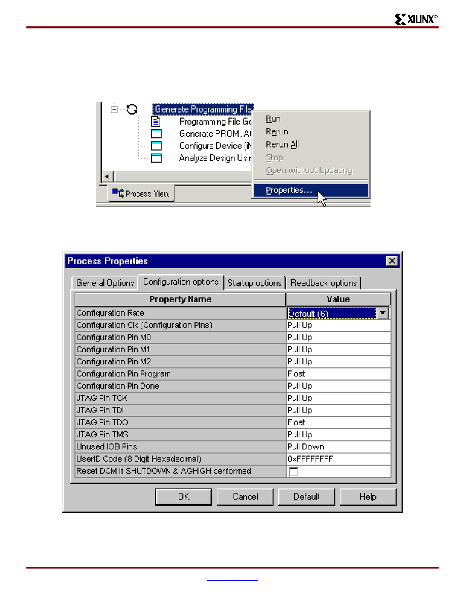
Spartan-3 1.2V FPGA Family: Pinout Descriptions
20
www.xilinx.com
DS099-4 (v1.2.2) October 9, 2003
1-800-255-7778
Advance Product Specification
R
Setting Options in Project Navigator
To set the bitstream generation options in Xilinx ISE Project
Navigator, right-click on the Generate Programming File
step in the Process View and click Properties, as shown in
Figure 5
.
Click the Configuration options tab and modify the avail-
able options as required by the application, as shown in
Figure 6
.
Figure 5: Setting Properties for Generate Programming File Step
DS099-4_05_030103
Figure 6: Configuration Option Settings
DS099-4_06_030103
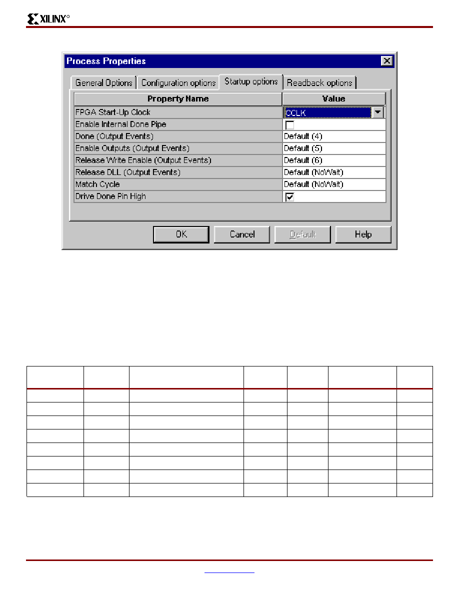
Spartan-3 1.2V FPGA Family: Pinout Descriptions
DS099-4 (v1.2.2) October 9, 2003
www.xilinx.com
21
Advance Product Specification
1-800-255-7778
R
To have the DONE pin drive High after successful configu-
ration, click the Startup options tab and check the Drive
Done Pin High box, as shown in
Figure 7
.
Click OK when finished.
Again, right-click on the Generate Programming File step
in the Process View. This time, choose Run or Rerun to
execute the changes.
Package Overview
Table 12
shows the eight, low-cost, space-saving produc-
tion packages for the Spartan-3 family. Not all Spartan-3
densities are available in all packages. However, for a spe-
cific package there is a common footprint for that supports
the various devices available in that package. See the foot-
print diagrams that follow.
Figure 7: Setting to Drive DONE Pin High after Configuration
DS099-4_07_030103
Table 12: Spartan-3 Family Package Options
Package
Leads
Type
Maximum
I/O
Pitch
(mm)
Area
(mm)
Height
(mm)
VQ100
100
Very-thin Quad Flat Pack
63
0.5
16 x 16
1.20
TQ144
144
Thin Quad Flat Pack
97
0.5
22 x 22
1.60
PQ208
208
Quad Flat Pack
141
0.5
30.6 x 30.6
4.10
FT256
256
Fine-pitch, Thin Ball Grid Array
173
1.0
17 x 17
1.55
FG456
456
Fine-pitch Ball Grid Array
333
1.0
23 x 23
2.60
FG676
676
Fine-pitch Ball Grid Array
405
1.0
27 x 27
2.60
FG900
900
Fine-pitch Ball Grid Array
549
1.0
31 x 31
2.60
FG1156
1156
Fine-pitch Ball Grid Array
692
1.0
35 x 35
2.60
Spartan-3 1.2V FPGA Family: Pinout Descriptions
22
www.xilinx.com
DS099-4 (v1.2.2) October 9, 2003
1-800-255-7778
Advance Product Specification
R
Detailed mechanical drawings for each package type are
available from the Xilinx web site at the specified location in
Table 13
.
Each package has three separate voltage supply
inputs--VCCINT, VCCAUX, and VCCO--and a common
ground return, GND. The numbers of pins dedicated to
these functions varies by package, as shown in
Table 14
.
A majority of package pins are user-defined I/O pins. How-
ever, the numbers and characteristics of these I/O depends
on the device type and the package in which it is available,
as shown in
Table 15
. The table shows the maximum num-
ber of single-ended I/O pins available, assuming that all
I/O-, DUAL-, DCI-, VREF-, and GCLK-type pins are used as
general-purpose I/O. Likewise, the table shows the maxi-
mum number of differential pin-pairs available on the pack-
age. Finally, the table shows how the total maximum user
I/Os are distributed by pin type, including the number of
unconnected--i.e., N.C.--pins on the device.
Table 13: Xilinx Package Mechanical Drawings
Package
Web Link (URL)
VQ100
http://www.xilinx.com/bvdocs/packages/vq100.pdf
TQ144
http://www.xilinx.com/bvdocs/packages/tq144.pdf
PQ208
http://www.xilinx.com/bvdocs/packages/pq208.pdf
FT256
http://www.xilinx.com/bvdocs/packages/ft256.pdf
FG456
http://www.xilinx.com/bvdocs/packages/fg456.pdf
FG676
http://www.xilinx.com/bvdocs/packages/fg676.pdf
FG900
http://www.xilinx.com/bvdocs/packages/fg900.pdf
FG1156
http://www.xilinx.com/bvdocs/packages/fg1156.pdf
Table 14: Power and Ground Supply Pins by Package
Package
VCCINT
VCCAUX
VCCO
GND
VQ100
4
4
8
10
TQ144
4
4
12
16
PQ208
4
8
12
28
FT256
8
8
24
32
FG456
12
8
40
52
FG676
20
16
64
76
FG900
32
24
80
120
FG1156
40
32
104
184
Table 15: Maximum User I/Os by Package
Device
Package
Maximum
User I/Os
Maximum
Differential
Pairs
All Possible I/O Pins by Type
N.C.
I/O
DUAL
DCI
VREF
GCLK
XC3S50
VQ100
63
29
22
12
14
7
8
0
XC3S200
VQ100
63
29
22
12
14
7
8
0
XC3S50
TQ144
97
46
51
12
14
12
8
0
XC3S200
TQ144
97
46
51
12
14
12
8
0
XC3S400
TQ144
97
46
51
12
14
12
8
0
XC3S50
PQ208
124
56
72
12
16
16
8
17
XC3S200
PQ208
141
62
83
12
16
22
8
0
XC3S400
PQ208
141
62
83
12
16
22
8
0
Spartan-3 1.2V FPGA Family: Pinout Descriptions
DS099-4 (v1.2.2) October 9, 2003
www.xilinx.com
23
Advance Product Specification
1-800-255-7778
R
Electronic versions of the package pinout tables and foot-
prints are available for download from the Xilinx web site.
Using a spreadsheet program, the data can be sorted and
reformatted according to any specific needs. Similarly, the
ASCII-text file is easily parsed by most scripting programs.
Download the files from the following location:
http://www.xilinx.com/bvdocs/publications/s3_pin.zip
XC3S200
FT256
173
76
113
12
16
24
8
0
XC3S400
FT256
173
76
113
12
16
24
8
0
XC3S1000
FT256
173
76
113
12
16
24
8
0
XC3S400
FG456
264
116
196
12
16
32
8
69
XC3S1000
FG456
333
149
261
12
16
36
8
0
XC3S1500
FG456
333
149
261
12
16
36
8
0
XC3S1000
FG676
391
175
315
12
16
40
8
98
XC3S1500
FG676
487
221
403
12
16
48
8
2
XC3S2000
FG676
489
221
405
12
16
48
8
0
XC3S2000
FG900
565
270
481
12
16
48
8
68
XC3S4000
FG900
633
300
549
12
16
48
8
0
XC3S5000
FG900
633
300
549
12
16
48
8
0
XC3S4000
FG1156
712
312
621
12
16
55
8
73
XC3S5000
FG1156
784
344
692
12
16
56
8
1
Table 15: Maximum User I/Os by Package (Continued)
Device
Package
Maximum
User I/Os
Maximum
Differential
Pairs
All Possible I/O Pins by Type
N.C.
I/O
DUAL
DCI
VREF
GCLK
Spartan-3 1.2V FPGA Family: Pinout Descriptions
24
www.xilinx.com
DS099-4 (v1.2.2) October 9, 2003
1-800-255-7778
Advance Product Specification
R
VQ100: 100-lead Very-thin Quad Flat
Package
The XC3S50 and the XC3S200 devices are available in the
100-lead very-thin quad flat package, VQ100. Both devices
share a common footprint for this package as shown in
Table 16
and
Figure 8
.
All the package pins appear in
Table 16
and are sorted by
bank number, then by pin name. Pairs of pins that form a dif-
ferential I/O pair appear together in the table. The table also
shows the pin number for each pin and the pin type, as
defined earlier.
Pinout Table
Table 16: VQ100 Package Pinout
Bank
XC3S50
XC3S200
Pin Name
VQ100 Pin
Number
Type
0
IO_L01N_0/VRP_0
P97
DCI
0
IO_L01P_0/VRN_0
P96
DCI
0
IO_L31N_0
P92
I/O
0
IO_L31P_0/VREF_0
P91
VREF
0
IO_L32N_0/GCLK7
P90
GCLK
0
IO_L32P_0/GCLK6
P89
GCLK
0
VCCO_0
P94
VCCO
1
IO
P81
I/O
1
IO_L01N_1/VRP_1
P80
DCI
1
IO_L01P_1/VRN_1
P79
DCI
1
IO_L31N_1/VREF_1
P86
VREF
1
IO_L31P_1
P85
I/O
1
IO_L32N_1/GCLK5
P88
GCLK
1
IO_L32P_1/GCLK4
P87
GCLK
1
VCCO_1
P83
VCCO
2
IO_L01N_2/VRP_2
P75
DCI
2
IO_L01P_2/VRN_2
P74
DCI
2
IO_L21N_2
P72
I/O
2
IO_L21P_2
P71
I/O
2
IO_L24N_2
P68
I/O
2
IO_L24P_2
P67
I/O
2
IO_L40N_2
P65
I/O
2
IO_L40P_2/VREF_2
P64
VREF
2
VCCO_2
P70
VCCO
3
IO
P55
I/O
3
IO
P59
I/O
3
IO_L01N_3/VRP_3
P54
DCI
3
IO_L01P_3/VRN_3
P53
DCI
3
IO_L24N_3
P61
I/O
3
IO_L24P_3
P60
I/O
3
IO_L40N_3/VREF_3
P63
VREF
3
IO_L40P_3
P62
I/O
3
VCCO_3
P57
VCCO
4
IO_L01N_4/VRP_4
P50
DCI
4
IO_L01P_4/VRN_4
P49
DCI
4
IO_L27N_4/DIN/D0
P48
DUAL
4
IO_L27P_4/D1
P47
DUAL
4
IO_L30N_4/D2
P44
DUAL
4
IO_L30P_4/D3
P43
DUAL
4
IO_L31N_4/INIT_B
P42
DUAL
4
IO_L31P_4/DOUT/BUSY
P40
DUAL
4
IO_L32N_4/GCLK1
P39
GCLK
4
IO_L32P_4/GCLK0
P38
GCLK
4
VCCO_4
P46
VCCO
5
IO_L01N_5/RDWR_B
P28
DUAL
5
IO_L01P_5/CS_B
P27
DUAL
5
IO_L28N_5/D6
P32
DUAL
5
IO_L28P_5/D7
P30
DUAL
5
IO_L31N_5/D4
P35
DUAL
5
IO_L31P_5/D5
P34
DUAL
5
IO_L32N_5/GCLK3
P37
GCLK
5
IO_L32P_5/GCLK2
P36
GCLK
5
VCCO_5
P31
VCCO
6
IO
P17
I/O
6
IO
P21
I/O
6
IO_L01N_6/VRP_6
P23
DCI
6
IO_L01P_6/VRN_6
P22
DCI
6
IO_L24N_6/VREF_6
P16
VREF
6
IO_L24P_6
P15
I/O
6
IO_L40N_6
P14
I/O
6
IO_L40P_6/VREF_6
P13
VREF
6
VCCO_6
P19
VCCO
7
IO_L01N_7/VRP_7
P2
DCI
7
IO_L01P_7/VRN_7
P1
DCI
7
IO_L21N_7
P5
I/O
7
IO_L21P_7
P4
I/O
7
IO_L23N_7
P9
I/O
7
IO_L23P_7
P8
I/O
7
IO_L40N_7/VREF_7
P12
VREF
7
IO_L40P_7
P11
I/O
Table 16: VQ100 Package Pinout
Bank
XC3S50
XC3S200
Pin Name
VQ100 Pin
Number
Type

Spartan-3 1.2V FPGA Family: Pinout Descriptions
DS099-4 (v1.2.2) October 9, 2003
www.xilinx.com
25
Advance Product Specification
1-800-255-7778
R
User I/Os by Bank
Table 17
indicates how the available user-I/O pins are dis-
tributed between the eight I/O banks on the VQ100 pack-
age.
7
VCCO_7
P6
VCCO
N/A
GND
P3
GND
N/A
GND
P10
GND
N/A
GND
P20
GND
N/A
GND
P29
GND
N/A
GND
P41
GND
N/A
GND
P56
GND
N/A
GND
P66
GND
N/A
GND
P73
GND
N/A
GND
P82
GND
N/A
GND
P95
GND
N/A
VCCAUX
P7
VCCAUX
N/A
VCCAUX
P33
VCCAUX
N/A
VCCAUX
P58
VCCAUX
N/A
VCCAUX
P84
VCCAUX
N/A
VCCINT
P18
VCCINT
N/A
VCCINT
P45
VCCINT
N/A
VCCINT
P69
VCCINT
Table 16: VQ100 Package Pinout
Bank
XC3S50
XC3S200
Pin Name
VQ100 Pin
Number
Type
N/A
VCCINT
P93
VCCINT
VCCAUX
CCLK
P52
CONFIG
VCCAUX
DONE
P51
CONFIG
VCCAUX
HSWAP_EN
P98
CONFIG
VCCAUX
M0
P25
CONFIG
VCCAUX
M1
P24
CONFIG
VCCAUX
M2
P26
CONFIG
VCCAUX
PROG_B
P99
CONFIG
VCCAUX
TCK
P77
JTAG
VCCAUX
TDI
P100
JTAG
VCCAUX
TDO
P76
JTAG
VCCAUX
TMS
P78
JTAG
Table 16: VQ100 Package Pinout
Bank
XC3S50
XC3S200
Pin Name
VQ100 Pin
Number
Type
Table 17: User I/Os Per Bank in VQ100 Package
Package Edge
I/O Bank
Maximum
I/O
All Possible I/O Pins by Type
I/O
DUAL
DCI
VREF
GCLK
Top
0
6
1
0
2
1
2
1
7
2
0
2
1
2
Right
2
8
5
0
2
1
0
3
8
5
0
2
1
0
Bottom
4
10
0
6
2
0
2
5
8
0
6
0
0
2
Left
6
8
4
0
2
2
0
7
8
5
0
2
1
0
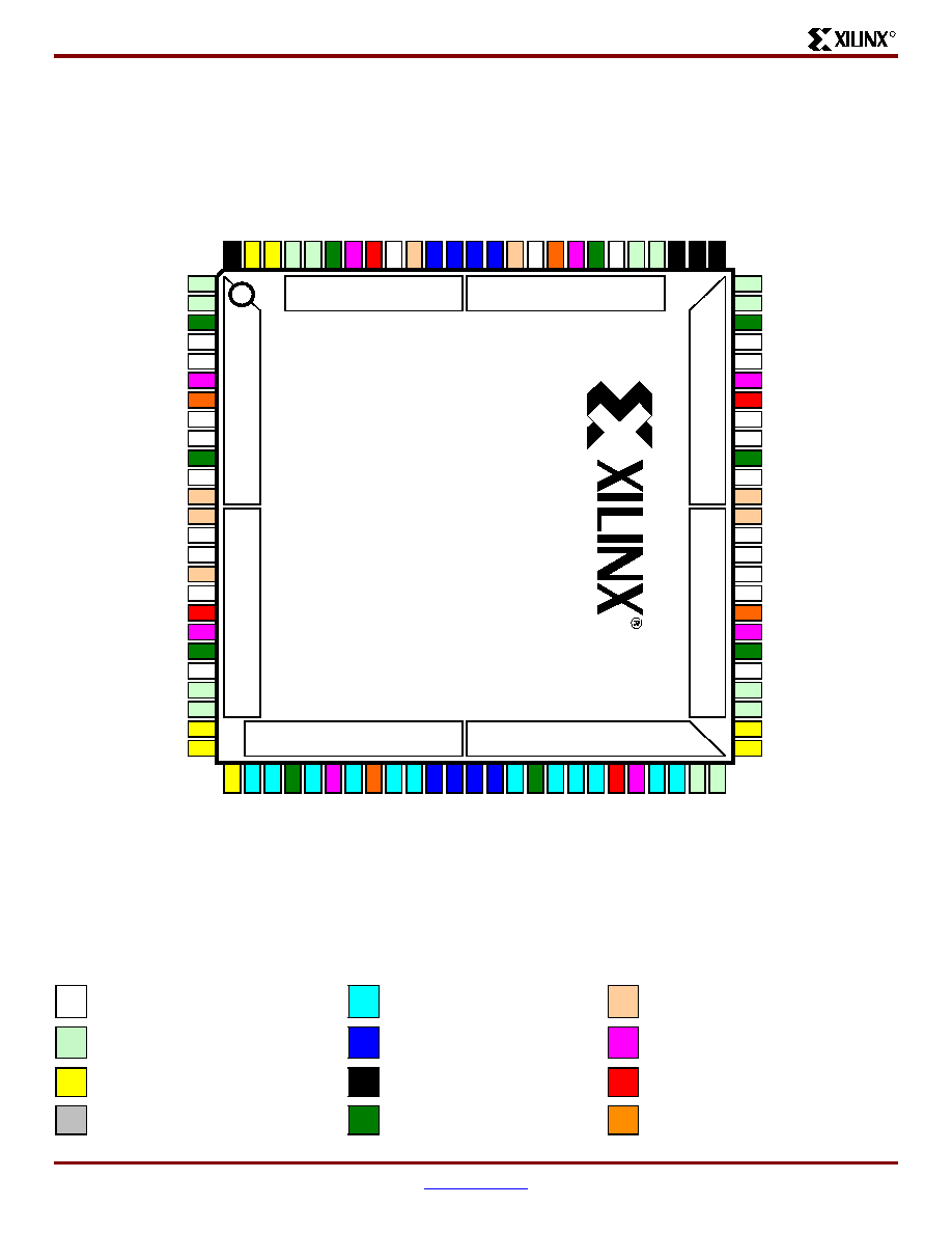
Spartan-3 1.2V FPGA Family: Pinout Descriptions
26
www.xilinx.com
DS099-4 (v1.2.2) October 9, 2003
1-800-255-7778
Advance Product Specification
R
VQ100 Footprint
Figure 8: VQ100 Package Footprint (top view). Note pin 1 indicator in top-left corner and logo orientation.
22
I/O: Unrestricted, general-purpose user I/O
12
DUAL: Configuration pin, then possible
user I/O
7
VREF: User I/O or input voltage reference for
bank
14
DCI: User I/O or reference resistor input for
bank
8
GCLK: User I/O or global clock buffer
input
8
VCCO: Output voltage supply for bank
7
CONFIG: Dedicated configuration pins
4
JTAG: Dedicated JTAG port pins
4
VCCINT: Internal core voltage supply (+1.2V)
0
N.C.: No unconnected pins in this package
10
GND: Ground
4
VCCAUX: Auxiliary voltage supply (+2.5V)
TDI
PROG_B
HSWAP_EN
IO_L01N_0/VRP_0
IO_L01P_0/VRN_0
GN
D
VCCO_0
VCCINT
IO_L31N_0
IO_L31P_0/VREF_0
IO_L32N_0/GCLK
7
IO_L32P_0/GCLK6
IO_L32N_1/GCLK
5
IO_L32P_1/GCLK4
IO_L31N_1/VREF_1
IO_L31P_1
VCCAUX
VCCO_1
GND
IO
IO_L01N_1/VRP_1
IO_L01P_1/VRN_1
TMS
TCK
TDO
100
99
98
97
96
95
94
93
92
91
90
89
88
87
86
85
84
83
82
81
80
79
78
77
76
1
75
IO_L01N_2/VRP_2
2
74
IO_L01P_2/VRN_2
3
73
GND
4
72
IO_L21N_2
5
71
IO_L21P_2
VCCO_7
6
70
VCCO_2
VCCAUX
7
69
VCCINT
8
68
IO_L24N_2
9
67
IO_L24P_2
10
66
GND
11
65
IO_L40N_2
12
64
IO_L40P_2/VREF_2
13
63
IO_L40N_3/VREF_3
14
62
IO_L40P_3
IO_L24P_6
IO_L40P_7
IO_L23P_7
IO_L21P_7
IO_L21N_7
IO_L23N_7
IO_L40N_6
15
61
IO_L24N_3
16
60
IO_L24P_3
IO
17
59
IO
VCCINT
18
58
VCCAUX
VCCO_6
19
57
VCCO_3
GND
GND
GND
IO_L01N_6/VRP_6
IO_L01P_6/VRN_6
IO_L24N_6/VREF_6
IO_L40N_7/VREF_7
IO_L01P_7/VRN_7
IO_L01N_7/VRP_7
IO_L40P_6/VREF_6
20
56
GND
IO
21
55
IO
22
54
IO_L01N_3/VRP_3
23
53
IO_L01P_3/VRN_3
M1
24
52
CCLK
M0
25
51
DONE
26
27
28
29
30
31
32
33
34
35
36
37
38
39
40
41
42
43
44
45
46
47
48
49
50
M2
IO_L01P_5/CS_B
IO_L01N_5/RDWR_B
GND
IO_L28P_5/D7
VCCO_5
IO_L28N_5/D6
VCCAUX
IO_L31P_5/D5
IO_L31N_5/D4
IO_L32P_5/GCLK2
IO_L32N_5/GCLK3
IO_L32P_4/GCLK0
IO_L32N_4/GCLK1
GND
IO_L31N_4/INIT_B
IO_L30P_4/D3
IO_L30N_4/D2
VCCINT
VCCO_4
IO_L27P_4/D1
IO_L27N_4/DIN/D0
IO_L31P_4/DOUT/BUSY
IO_L01P_4/VRN_4
IO_L01N_4/VRP_4
Bank 6
Bank 0
Bank 1
Bank 3
B
ank 2
Bank 4
(no VREF)
Bank 5
(
no VREF, no DCI)
Bank 7
DS099-4_15_042303
Spartan-3 1.2V FPGA Family: Pinout Descriptions
DS099-4 (v1.2.2) October 9, 2003
www.xilinx.com
27
Advance Product Specification
1-800-255-7778
R
TQ144: 144-lead Thin Quad Flat
Package
The XC3S50, the XC3S200, and the XC3S400 are avail-
able in the 144-lead thin quad flat package, TQ144. Conse-
quently, there is only one footprint for this package as shown
in
Table 18
and
Figure 9
.
The TQ144 package only has four separate VCCO inputs,
unlike the other packages, which have eight separate
VCCO inputs. The TQ144 package has a separate VCCO
input for the top, bottom, left, and right. However, there are
still eight separate I/O banks, as shown in
Table 18
and
Figure 9
. Banks 0 and 1 share the VCCO_TOP input, Banks
2 and 3 share the VCCO_RIGHT input, Banks 4 and 5
share the VCCO_BOTTOM input, and Banks 6 and 7 share
the VCCO_LEFT input.
All the package pins appear in
Table 18
and are sorted by
bank number, then by pin name. Pairs of pins that form a dif-
ferential I/O pair appear together in the table. The table also
shows the pin number for each pin and the pin type, as
defined earlier.
Pinout Table
Table 18: TQ144 Package Pinout
Bank
XC3S50
XC3S200
XC3S400
Pin Name
TQ144 Pin
Number
Type
0
IO_L01N_0/VRP_0
P141
DCI
0
IO_L01P_0/VRN_0
P140
DCI
0
IO_L27N_0
P137
I/O
0
IO_L27P_0
P135
I/O
0
IO_L30N_0
P132
I/O
0
IO_L30P_0
P131
I/O
0
IO_L31N_0
P130
I/O
0
IO_L31P_0/VREF_0
P129
VREF
0
IO_L32N_0/GCLK7
P128
GCLK
0
IO_L32P_0/GCLK6
P127
GCLK
1
IO
P116
I/O
1
IO_L01N_1/VRP_1
P113
DCI
1
IO_L01P_1/VRN_1
P112
DCI
1
IO_L28N_1
P119
I/O
1
IO_L28P_1
P118
I/O
1
IO_L31N_1/VREF_1
P123
VREF
1
IO_L31P_1
P122
I/O
1
IO_L32N_1/GCLK5
P125
GCLK
1
IO_L32P_1/GCLK4
P124
GCLK
2
IO_L01N_2/VRP_2
P108
DCI
2
IO_L01P_2/VRN_2
P107
DCI
2
IO_L20N_2
P105
I/O
2
IO_L20P_2
P104
I/O
2
IO_L21N_2
P103
I/O
2
IO_L21P_2
P102
I/O
2
IO_L22N_2
P100
I/O
2
IO_L22P_2
P99
I/O
2
IO_L23N_2/VREF_2
P98
VREF
2
IO_L23P_2
P97
I/O
2
IO_L24N_2
P96
I/O
2
IO_L24P_2
P95
I/O
2
IO_L40N_2
P93
I/O
2
IO_L40P_2/VREF_2
P92
VREF
3
IO
P76
I/O
3
IO_L01N_3/VRP_3
P74
DCI
3
IO_L01P_3/VRN_3
P73
DCI
3
IO_L20N_3
P78
I/O
3
IO_L20P_3
P77
I/O
3
IO_L21N_3
P80
I/O
3
IO_L21P_3
P79
I/O
3
IO_L22N_3
P83
I/O
3
IO_L22P_3
P82
I/O
3
IO_L23N_3
P85
I/O
3
IO_L23P_3/VREF_3
P84
VREF
3
IO_L24N_3
P87
I/O
3
IO_L24P_3
P86
I/O
3
IO_L40N_3/VREF_3
P90
VREF
3
IO_L40P_3
P89
I/O
4
IO/VREF_4
P70
VREF
4
IO_L01N_4/VRP_4
P69
DCI
4
IO_L01P_4/VRN_4
P68
DCI
4
IO_L27N_4/DIN/D0
P65
DUAL
4
IO_L27P_4/D1
P63
DUAL
4
IO_L30N_4/D2
P60
DUAL
4
IO_L30P_4/D3
P59
DUAL
4
IO_L31N_4/INIT_B
P58
DUAL
4
IO_L31P_4/DOUT/BUSY
P57
DUAL
4
IO_L32N_4/GCLK1
P56
GCLK
4
IO_L32P_4/GCLK0
P55
GCLK
5
IO/VREF_5
P44
VREF
5
IO_L01N_5/RDWR_B
P41
DUAL
5
IO_L01P_5/CS_B
P40
DUAL
5
IO_L28N_5/D6
P47
DUAL
Table 18: TQ144 Package Pinout (Continued)
Bank
XC3S50
XC3S200
XC3S400
Pin Name
TQ144 Pin
Number
Type
Spartan-3 1.2V FPGA Family: Pinout Descriptions
28
www.xilinx.com
DS099-4 (v1.2.2) October 9, 2003
1-800-255-7778
Advance Product Specification
R
5
IO_L28P_5/D7
P46
DUAL
5
IO_L31N_5/D4
P51
DUAL
5
IO_L31P_5/D5
P50
DUAL
5
IO_L32N_5/GCLK3
P53
GCLK
5
IO_L32P_5/GCLK2
P52
GCLK
6
IO_L01N_6/VRP_6
P36
DCI
6
IO_L01P_6/VRN_6
P35
DCI
6
IO_L20N_6
P33
I/O
6
IO_L20P_6
P32
I/O
6
IO_L21N_6
P31
I/O
6
IO_L21P_6
P30
I/O
6
IO_L22N_6
P28
I/O
6
IO_L22P_6
P27
I/O
6
IO_L23N_6
P26
I/O
6
IO_L23P_6
P25
I/O
6
IO_L24N_6/VREF_6
P24
VREF
6
IO_L24P_6
P23
I/O
6
IO_L40N_6
P21
I/O
6
IO_L40P_6/VREF_6
P20
VREF
7
IO/VREF_7
P4
VREF
7
IO_L01N_7/VRP_7
P2
DCI
7
IO_L01P_7/VRN_7
P1
DCI
7
IO_L20N_7
P6
I/O
7
IO_L20P_7
P5
I/O
7
IO_L21N_7
P8
I/O
7
IO_L21P_7
P7
I/O
7
IO_L22N_7
P11
I/O
7
IO_L22P_7
P10
I/O
7
IO_L23N_7
P13
I/O
7
IO_L23P_7
P12
I/O
7
IO_L24N_7
P15
I/O
7
IO_L24P_7
P14
I/O
7
IO_L40N_7/VREF_7
P18
VREF
7
IO_L40P_7
P17
I/O
0,1
VCCO_TOP
P126
VCCO
0,1
VCCO_TOP
P138
VCCO
0,1
VCCO_TOP
P115
VCCO
2,3
VCCO_RIGHT
P106
VCCO
2,3
VCCO_RIGHT
P75
VCCO
2,3
VCCO_RIGHT
P91
VCCO
4,5
VCCO_BOTTOM
P54
VCCO
Table 18: TQ144 Package Pinout (Continued)
Bank
XC3S50
XC3S200
XC3S400
Pin Name
TQ144 Pin
Number
Type
4,5
VCCO_BOTTOM
P43
VCCO
4,5
VCCO_BOTTOM
P66
VCCO
6,7
VCCO_LEFT
P19
VCCO
6,7
VCCO_LEFT
P34
VCCO
6,7
VCCO_LEFT
P3
VCCO
N/A
GND
P136
GND
N/A
GND
P139
GND
N/A
GND
P114
GND
N/A
GND
P117
GND
N/A
GND
P94
GND
N/A
GND
P101
GND
N/A
GND
P81
GND
N/A
GND
P88
GND
N/A
GND
P64
GND
N/A
GND
P67
GND
N/A
GND
P42
GND
N/A
GND
P45
GND
N/A
GND
P22
GND
N/A
GND
P29
GND
N/A
GND
P9
GND
N/A
GND
P16
GND
N/A
VCCAUX
P134
VCCAUX
N/A
VCCAUX
P120
VCCAUX
N/A
VCCAUX
P62
VCCAUX
N/A
VCCAUX
P48
VCCAUX
N/A
VCCINT
P133
VCCINT
N/A
VCCINT
P121
VCCINT
N/A
VCCINT
P61
VCCINT
N/A
VCCINT
P49
VCCINT
VCCAUX
CCLK
P72
CONFIG
VCCAUX
DONE
P71
CONFIG
VCCAUX
HSWAP_EN
P142
CONFIG
VCCAUX
M0
P38
CONFIG
VCCAUX
M1
P37
CONFIG
VCCAUX
M2
P39
CONFIG
VCCAUX
PROG_B
P143
CONFIG
VCCAUX
TCK
P110
JTAG
VCCAUX
TDI
P144
JTAG
VCCAUX
TDO
P109
JTAG
VCCAUX
TMS
P111
JTAG
Table 18: TQ144 Package Pinout (Continued)
Bank
XC3S50
XC3S200
XC3S400
Pin Name
TQ144 Pin
Number
Type
Spartan-3 1.2V FPGA Family: Pinout Descriptions
DS099-4 (v1.2.2) October 9, 2003
www.xilinx.com
29
Advance Product Specification
1-800-255-7778
R
User I/Os by Bank
Table 19
indicates how the available user-I/O pins are dis-
tributed between the eight I/O banks on the TQ144 pack-
age.
Table 19: User I/Os Per Bank in TQ144 Package
Package Edge
I/O Bank
Maximum
I/O
All Possible I/O Pins by Type
I/O
DUAL
DCI
VREF
GCLK
Top
0
10
5
0
2
1
2
1
9
4
0
2
1
2
Right
2
14
10
0
2
2
0
3
15
11
0
2
2
0
Bottom
4
11
0
6
2
1
2
5
9
0
6
0
1
2
Left
6
14
10
0
2
2
0
7
15
11
0
2
2
0
Spartan-3 1.2V FPGA Family: Pinout Descriptions
30
www.xilinx.com
DS099-4 (v1.2.2) October 9, 2003
1-800-255-7778
Advance Product Specification
R
TQ144 Footprint
Figure 9: TQ144 Package Footprint (top view). Note pin 1 indicator in top-left corner and logo orientation.
51
I/O: Unrestricted, general-purpose user I/O
12
DUAL: Configuration pin, then possible
user I/O
12
VREF: User I/O or input voltage reference for
bank
14
DCI: User I/O or reference resistor input for
bank
8
GCLK: User I/O or global clock buffer
input
12
VCCO: Output voltage supply for bank
7
CONFIG: Dedicated configuration pins
4
JTAG: Dedicated JTAG port pins
4
VCCINT: Internal core voltage supply (+1.2V)
0
N.C.: No unconnected pins in this package
16
GND: Ground
4
VCCAUX: Auxiliary voltage supply (+2.5V)
IO
TD
I
PROG_
B
HSW
AP_EN
I
O
_L01N_0/
VRP_
0
I
O
_L01P_0/
VRN_
0
GN
D
VCCO_TOP
I
O
_L27N_0
GN
D
I
O
_L27P_0
VCCAUX
VCCINT
I
O
_L30N_0
I
O
_L30P_0
I
O
_L31N_0
I
O
_L31P_0/
VREF_0
I
O
_L32N_0
/
G
C
LK
7
I
O
_L32P_0
/
G
C
LK
6
VCCO_TOP
I
O
_L32N_1
/
G
C
LK
5
I
O
_L32P_1
/
G
C
LK
4
I
O
_L31N_1/
VREF_1
I
O
_L31P_1
VCCINT
VCCAUX
I
O
_L28N_
1
I
O
_L28P_
1
GN
D
IO
VCCO_TOP
GN
D
I
O
_L01N_1/
VRP_
1
I
O
_L01P_1/
VRN_
1
TM
S
TC
K
TD
O
144
143
142
141
140
139
138
137
136
135
134
133
132
131
130
129
128
127
126
125
124
123
122
121
120
119
118
117
116
115
114
113
112
111
110
109
IO_L01P_7/VRN_7
1
108
IO_L01N_2/VRP_2
IO_L01N_7/VRP_7
2
107
IO_L01P_2/VRN_2
VCCO_LEFT
3
X
106
VCCO_RIGHT
IO/VREF_7
4
105
IO_L20N_2
IO_L20P_7
5
104
IO_L20P_2
IO_L20N_7
6
103
IO_L21N_2
IO_L21P_7
7
102
IO_L21P_2
IO_L21N_7
8
101
GND
GN D
9
100
IO_L22N_2
IO_L22P_7
10
99
IO_L22P_2
IO_L22N_7
11
98
IO_L23N_2/VREF_2
IO_L23P_7
12
97
IO_L23P_2
IO_L23N_7
13
96
IO_L24N_2
IO_L24P_7
14
95
IO_L24P_2
IO_L24N_7
15
94
GND
GN D
16
93
IO_L40N_2
IO_L40P_7
17
92
IO_L40P_2/VREF_2
IO_L40N_7/VREF_7
18
91
VCCO_RIGHT
VCCO_LEFT
19
90
IO_L40N_3/VREF_3
IO_L40P_6/VREF_6
20
8
9
IO_L40P_3
IO_L40N_6
21
88
GND
GN D
22
8
7
IO_L24N_3
IO_L24P_6
23
8
6
IO_L24P_3
IO_L24N_6/VREF_6
24
8
5
IO_L23N_3
IO_L23P_6
25
8
4
IO_L23P_3/VREF_3
IO_L23N_6
26
8
3
IO_L22N_3
IO_L22P_6
27
8
2
IO_L22P_3
IO_L22N_6
28
81
GND
GN D
29
8
0
IO_L21N_3
IO_L21P_6
30
79
IO_L21P_3
IO_L21N_6
31
78
IO_L20N_3
IO_L20P_6
32
77
IO_L20P_3
IO_L20N_6
33
76
IO
VCCO_LEFT
34
75
VCCO_RIGHT
IO_L01P_6/VRN_6
35
74
IO_L01N_3/VRP_3
IO_L01N_6/VRP_6
36
73
IO_L01P_3/VRN_3
37
38
39
40
41
42
43
44
45
46
47
48
49
50
51
52
53
54
55
56
57
58
59
60
61
62
63
64
65
66
67
68
69
70
71
72
M1
M0
M2
I
O
_L01P_5/
CS_B
_L01N_5/
RDW
R_
B
GN
D
VCCO_BOTTOM
IO/VREF_
5
GN
D
I
O
_L28P_5/
D7
I
O
_L28N_5/
D6
VCCAUX
VCCINT
I
O
_L31P_5/
D5
I
O
_L31N_5/
D4
I
O
_L32P_5
/
G
C
LK
2
I
O
_L32N_5
/
G
C
LK
3
VCCO_BOTTO
M
I
O
_L32P_4
/
G
C
LK
0
I
O
_L32N_4
/
G
C
LK
1
_
IO_L31P
4/
DOUT
/BUSY
I
O
_L31N_4
/INIT
_
B
I
O
_L30P_4/
D3
I
O
_L30N_4/
D2
VCCINT
VCCAUX
I
O
_L27P_4/
D1
GN
D
I
O
_L27N_4/
DIN/D0
VCCO_BOTTO
M
GN
D
I
O
_L01P_4/
VRN_
4
I
O
_L01N_4/
VRP_
4
IO/VREF_
4
DONE
CCL
K
Bank 5
(no DCI)
Bank 3
B
ank 2
VCCO for
Top Edge
VCCO for Right Edge
VCCO for Bottom Edge
Bank 0
Bank 1
Bank 7
Bank 4
Bank 6
VCCO for Left Edge
DS099-4_08_030503

Spartan-3 1.2V FPGA Family: Pinout Descriptions
DS099-4 (v1.2.2) October 9, 2003
www.xilinx.com
31
Advance Product Specification
1-800-255-7778
R
PQ208: 208-lead Plastic Quad Flat Pack
The 208-lead plastic quad flat package, PQ208, supports
three different Spartan-3 devices, including the XC3S50,
the XC3S200, and the XC3S400. The footprints for the
XC3S200 and XC3S400 are identical, as shown in
Table 20
and
Figure 10
. The XC3S50, however, has fewer I/O pins
resulting in 17 unconnected pins on the PQ208 package,
labeled as "N.C." In
Table 20
and
Figure 10
, these uncon-
nected pins are indicated with a black diamond symbol (
).
All the package pins appear in
Table 20
and are sorted by
bank number, then by pin name. Pairs of pins that form a dif-
ferential I/O pair appear together in the table. The table also
shows the pin number for each pin and the pin type, as
defined earlier.
If there is a difference between the XC3S50 pinout and the
pinout for the XC3S200 and XC3S400, then that difference
is highlighted in
Table 20
. If the table entry is shaded grey,
then there is an unconnected pin on the XC3S50 that maps
to a user-I/O pin on the XC3S200 and XC3S400. If the table
entry is shaded tan, then the unconnected pin on the
XC3S50 maps to a VREF-type pin on the XC3S200 and
XC3S400. If the other VREF pins in the bank all connect to
a voltage reference to support a special I/O standard, then
also connect the N.C. pin on the XC3S50 to the same VREF
voltage. This provides maximum flexibility as you could
potentially migrate a design from the XC3S50 device to an
XC3S200 or XC3S400 FPGA without changing the printed
circuit board.
Pinout Table
Table 20: PQ208 Package Pinout
Bank
XC3S50
Pin Name
XC3S200
XC3S400
Pin Name
PQ208
Pin
Number
Type
0
IO
IO
P189
I/O
0
IO
IO
P197
I/O
0
N.C. (
)
IO/VREF_0
P200
VREF
0
IO/VREF_0
IO/VREF_0
P205
VREF
0
IO_L01N_0/
VRP_0
IO_L01N_0/
VRP_0
P204
DCI
0
IO_L01P_0/
VRN_0
IO_L01P_0/
VRN_0
P203
DCI
0
IO_L25N_0
IO_L25N_0
P199
I/O
0
IO_L25P_0
IO_L25P_0
P198
I/O
0
IO_L27N_0
IO_L27N_0
P196
I/O
0
IO_L27P_0
IO_L27P_0
P194
I/O
0
IO_L30N_0
IO_L30N_0
P191
I/O
0
IO_L30P_0
IO_L30P_0
P190
I/O
0
IO_L31N_0
IO_L31N_0
P187
I/O
0
IO_L31P_0/
VREF_0
IO_L31P_0/
VREF_0
P185
VREF
0
IO_L32N_0/
GCLK7
IO_L32N_0/
GCLK7
P184
GCLK
0
IO_L32P_0/
GCLK6
IO_L32P_0/
GCLK6
P183
GCLK
0
VCCO_0
VCCO_0
P188
VCCO
0
VCCO_0
VCCO_0
P201
VCCO
1
IO
IO
P167
I/O
1
IO
IO
P175
I/O
1
IO
IO
P182
I/O
1
IO_L01N_1/
VRP_1
IO_L01N_1/
VRP_1
P162
DCI
1
IO_L01P_1/
VRN_1
IO_L01P_1/
VRN_1
P161
DCI
1
IO_L10N_1/
VREF_1
IO_L10N_1/
VREF_1
P166
VREF
1
IO_L10P_1
IO_L10P_1
P165
I/O
1
IO_L27N_1
IO_L27N_1
P169
I/O
1
IO_L27P_1
IO_L27P_1
P168
I/O
1
IO_L28N_1
IO_L28N_1
P172
I/O
1
IO_L28P_1
IO_L28P_1
P171
I/O
1
IO_L31N_1/
VREF_1
IO_L31N_1/
VREF_1
P178
VREF
1
IO_L31P_1
IO_L31P_1
P176
I/O
1
IO_L32N_1/
GCLK5
IO_L32N_1/
GCLK5
P181
GCLK
1
IO_L32P_1/
GCLK4
IO_L32P_1/
GCLK4
P180
GCLK
1
VCCO_1
VCCO_1
P164
VCCO
1
VCCO_1
VCCO_1
P177
VCCO
2
N.C. (
)
IO/VREF_2
P154
VREF
2
IO_L01N_2/
VRP_2
IO_L01N_2/
VRP_2
P156
DCI
2
IO_L01P_2/
VRN_2
IO_L01P_2/
VRN_2
P155
DCI
2
IO_L19N_2
IO_L19N_2
P152
I/O
2
IO_L19P_2
IO_L19P_2
P150
I/O
2
IO_L20N_2
IO_L20N_2
P149
I/O
2
IO_L20P_2
IO_L20P_2
P148
I/O
2
IO_L21N_2
IO_L21N_2
P147
I/O
2
IO_L21P_2
IO_L21P_2
P146
I/O
2
IO_L22N_2
IO_L22N_2
P144
I/O
2
IO_L22P_2
IO_L22P_2
P143
I/O
2
IO_L23N_2/
VREF_2
IO_L23N_2/
VREF_2
P141
VREF
2
IO_L23P_2
IO_L23P_2
P140
I/O
Table 20: PQ208 Package Pinout (Continued)
Bank
XC3S50
Pin Name
XC3S200
XC3S400
Pin Name
PQ208
Pin
Number
Type

Spartan-3 1.2V FPGA Family: Pinout Descriptions
32
www.xilinx.com
DS099-4 (v1.2.2) October 9, 2003
1-800-255-7778
Advance Product Specification
R
2
IO_L24N_2
IO_L24N_2
P139
I/O
2
IO_L24P_2
IO_L24P_2
P138
I/O
2
N.C. (
)
IO_L39N_2
P137
I/O
2
N.C. (
)
IO_L39P_2
P135
I/O
2
IO_L40N_2
IO_L40N_2
P133
I/O
2
IO_L40P_2/
VREF_2
IO_L40P_2/
VREF_2
P132
VREF
2
VCCO_2
VCCO_2
P136
VCCO
2
VCCO_2
VCCO_2
P153
VCCO
3
IO_L01N_3/
VRP_3
IO_L01N_3/
VRP_3
P107
DCI
3
IO_L01P_3/
VRN_3
IO_L01P_3/
VRN_3
P106
DCI
3
N.C. (
)
IO_L17N_3
P109
I/O
3
N.C. (
)
IO_L17P_3/
VREF_3
P108
VREF
3
IO_L19N_3
IO_L19N_3
P113
I/O
3
IO_L19P_3
IO_L19P_3
P111
I/O
3
IO_L20N_3
IO_L20N_3
P115
I/O
3
IO_L20P_3
IO_L20P_3
P114
I/O
3
IO_L21N_3
IO_L21N_3
P117
I/O
3
IO_L21P_3
IO_L21P_3
P116
I/O
3
IO_L22N_3
IO_L22N_3
P120
I/O
3
IO_L22P_3
IO_L22P_3
P119
I/O
3
IO_L23N_3
IO_L23N_3
P123
I/O
3
IO_L23P_3/
VREF_3
IO_L23P_3/
VREF_3
P122
VREF
3
IO_L24N_3
IO_L24N_3
P125
I/O
3
IO_L24P_3
IO_L24P_3
P124
I/O
3
N.C. (
)
IO_L39N_3
P128
I/O
3
N.C. (
)
IO_L39P_3
P126
I/O
3
IO_L40N_3/
VREF_3
IO_L40N_3/
VREF_3
P131
VREF
3
IO_L40P_3
IO_L40P_3
P130
I/O
3
VCCO_3
VCCO_3
P110
VCCO
3
VCCO_3
VCCO_3
P127
VCCO
4
IO
IO
P93
I/O
4
N.C. (
)
IO
P97
I/O
4
IO/VREF_4
IO/VREF_4
P85
VREF
4
N.C. (
)
IO/VREF_4
P96
VREF
4
IO/VREF_4
IO/VREF_4
P102
VREF
4
IO_L01N_4/
VRP_4
IO_L01N_4/
VRP_4
P101
DCI
Table 20: PQ208 Package Pinout (Continued)
Bank
XC3S50
Pin Name
XC3S200
XC3S400
Pin Name
PQ208
Pin
Number
Type
4
IO_L01P_4/
VRN_4
IO_L01P_4/
VRN_4
P100
DCI
4
IO_L25N_4
IO_L25N_4
P95
I/O
4
IO_L25P_4
IO_L25P_4
P94
I/O
4
IO_L27N_4/
DIN/D0
IO_L27N_4/
DIN/D0
P92
DUAL
4
IO_L27P_4/
D1
IO_L27P_4/
D1
P90
DUAL
4
IO_L30N_4/
D2
IO_L30N_4/
D2
P87
DUAL
4
IO_L30P_4/
D3
IO_L30P_4/
D3
P86
DUAL
4
IO_L31N_4/
INIT_B
IO_L31N_4/
INIT_B
P83
DUAL
4
IO_L31P_4/
DOUT/BUSY
IO_L31P_4/
DOUT/BUSY
P81
DUAL
4
IO_L32N_4/
GCLK1
IO_L32N_4/
GCLK1
P80
GCLK
4
IO_L32P_4/
GCLK0
IO_L32P_4/
GCLK0
P79
GCLK
4
VCCO_4
VCCO_4
P84
VCCO
4
VCCO_4
VCCO_4
P98
VCCO
5
IO
IO
P63
I/O
5
IO
IO
P71
I/O
5
IO/VREF_5
IO/VREF_5
P78
VREF
5
IO_L01N_5/
RDWR_B
IO_L01N_5/
RDWR_B
P58
DUAL
5
IO_L01P_5/
CS_B
IO_L01P_5/
CS_B
P57
DUAL
5
IO_L10N_5/
VRP_5
IO_L10N_5/
VRP_5
P62
DCI
5
IO_L10P_5/
VRN_5
IO_L10P_5/
VRN_5
P61
DCI
5
IO_L27N_5/
VREF_5
IO_L27N_5/
VREF_5
P65
VREF
5
IO_L27P_5
IO_L27P_5
P64
I/O
5
IO_L28N_5/
D6
IO_L28N_5/
D6
P68
DUAL
5
IO_L28P_5/
D7
IO_L28P_5/
D7
P67
DUAL
5
IO_L31N_5/
D4
IO_L31N_5/
D4
P74
DUAL
5
IO_L31P_5/
D5
IO_L31P_5/
D5
P72
DUAL
5
IO_L32N_5/
GCLK3
IO_L32N_5/
GCLK3
P77
GCLK
Table 20: PQ208 Package Pinout (Continued)
Bank
XC3S50
Pin Name
XC3S200
XC3S400
Pin Name
PQ208
Pin
Number
Type

Spartan-3 1.2V FPGA Family: Pinout Descriptions
DS099-4 (v1.2.2) October 9, 2003
www.xilinx.com
33
Advance Product Specification
1-800-255-7778
R
5
IO_L32P_5/
GCLK2
IO_L32P_5/
GCLK2
P76
GCLK
5
VCCO_5
VCCO_5
P60
VCCO
5
VCCO_5
VCCO_5
P73
VCCO
6
N.C. (
)
IO/VREF_6
P50
VREF
6
IO_L01N_6/
VRP_6
IO_L01N_6/
VRP_6
P52
DCI
6
IO_L01P_6/
VRN_6
IO_L01P_6/
VRN_6
P51
DCI
6
IO_L19N_6
IO_L19N_6
P48
I/O
6
IO_L19P_6
IO_L19P_6
P46
I/O
6
IO_L20N_6
IO_L20N_6
P45
I/O
6
IO_L20P_6
IO_L20P_6
P44
I/O
6
IO_L21N_6
IO_L21N_6
P43
I/O
6
IO_L21P_6
IO_L21P_6
P42
I/O
6
IO_L22N_6
IO_L22N_6
P40
I/O
6
IO_L22P_6
IO_L22P_6
P39
I/O
6
IO_L23N_6
IO_L23N_6
P37
I/O
6
IO_L23P_6
IO_L23P_6
P36
I/O
6
IO_L24N_6/
VREF_6
IO_L24N_6/
VREF_6
P35
VREF
6
IO_L24P_6
IO_L24P_6
P34
I/O
6
N.C. (
)
IO_L39N_6
P33
I/O
6
N.C. (
)
IO_L39P_6
P31
I/O
6
IO_L40N_6
IO_L40N_6
P29
I/O
6
IO_L40P_6/
VREF_6
IO_L40P_6/
VREF_6
P28
VREF
6
VCCO_6
VCCO_6
P32
VCCO
6
VCCO_6
VCCO_6
P49
VCCO
7
IO_L01N_7/
VRP_7
IO_L01N_7/
VRP_7
P3
DCI
7
IO_L01P_7/
VRN_7
IO_L01P_7/
VRN_7
P2
DCI
7
N.C. (
)
IO_L16N_7
P5
I/O
7
N.C. (
)
IO_L16P_7/
VREF_7
P4
VREF
7
IO_L19N_7/
VREF_7
IO_L19N_7/
VREF_7
P9
VREF
7
IO_L19P_7
IO_L19P_7
P7
I/O
7
IO_L20N_7
IO_L20N_7
P11
I/O
7
IO_L20P_7
IO_L20P_7
P10
I/O
7
IO_L21N_7
IO_L21N_7
P13
I/O
7
IO_L21P_7
IO_L21P_7
P12
I/O
7
IO_L22N_7
IO_L22N_7
P16
I/O
Table 20: PQ208 Package Pinout (Continued)
Bank
XC3S50
Pin Name
XC3S200
XC3S400
Pin Name
PQ208
Pin
Number
Type
7
IO_L22P_7
IO_L22P_7
P15
I/O
7
IO_L23N_7
IO_L23N_7
P19
I/O
7
IO_L23P_7
IO_L23P_7
P18
I/O
7
IO_L24N_7
IO_L24N_7
P21
I/O
7
IO_L24P_7
IO_L24P_7
P20
I/O
7
N.C. (
)
IO_L39N_7
P24
I/O
7
N.C. (
)
IO_L39P_7
P22
I/O
7
IO_L40N_7/
VREF_7
IO_L40N_7/
VREF_7
P27
VREF
7
IO_L40P_7
IO_L40P_7
P26
I/O
7
VCCO_7
VCCO_7
P6
VCCO
7
VCCO_7
VCCO_7
P23
VCCO
N/A
GND
GND
P1
GND
N/A
GND
GND
P186
GND
N/A
GND
GND
P195
GND
N/A
GND
GND
P202
GND
N/A
GND
GND
P163
GND
N/A
GND
GND
P170
GND
N/A
GND
GND
P179
GND
N/A
GND
GND
P134
GND
N/A
GND
GND
P145
GND
N/A
GND
GND
P151
GND
N/A
GND
GND
P157
GND
N/A
GND
GND
P112
GND
N/A
GND
GND
P118
GND
N/A
GND
GND
P129
GND
N/A
GND
GND
P82
GND
N/A
GND
GND
P91
GND
N/A
GND
GND
P99
GND
N/A
GND
GND
P105
GND
N/A
GND
GND
P53
GND
N/A
GND
GND
P59
GND
N/A
GND
GND
P66
GND
N/A
GND
GND
P75
GND
N/A
GND
GND
P30
GND
N/A
GND
GND
P41
GND
N/A
GND
GND
P47
GND
N/A
GND
GND
P8
GND
N/A
GND
GND
P14
GND
N/A
GND
GND
P25
GND
N/A
VCCAUX
VCCAUX
P193
VCCAUX
N/A
VCCAUX
VCCAUX
P173
VCCAUX
Table 20: PQ208 Package Pinout (Continued)
Bank
XC3S50
Pin Name
XC3S200
XC3S400
Pin Name
PQ208
Pin
Number
Type

Spartan-3 1.2V FPGA Family: Pinout Descriptions
34
www.xilinx.com
DS099-4 (v1.2.2) October 9, 2003
1-800-255-7778
Advance Product Specification
R
User I/Os by Bank
Table 21
indicates how the available user-I/O pins are dis-
tributed between the eight I/O banks for the XC3S50 in the
PQ208 package. Similarly,
Table 22
shows how the avail-
able user-I/O pins are distributed between the eight I/O
banks for the XC3S200 and XC3S400 in the PQ208 pack-
age.
N/A
VCCAUX
VCCAUX
P142
VCCAUX
N/A
VCCAUX
VCCAUX
P121
VCCAUX
N/A
VCCAUX
VCCAUX
P89
VCCAUX
N/A
VCCAUX
VCCAUX
P69
VCCAUX
N/A
VCCAUX
VCCAUX
P38
VCCAUX
N/A
VCCAUX
VCCAUX
P17
VCCAUX
N/A
VCCINT
VCCINT
P192
VCCINT
N/A
VCCINT
VCCINT
P174
VCCINT
N/A
VCCINT
VCCINT
P88
VCCINT
N/A
VCCINT
VCCINT
P70
VCCINT
VCCAUX CCLK
CCLK
P104
CONFIG
VCCAUX DONE
DONE
P103
CONFIG
VCCAUX HSWAP_EN
HSWAP_EN
P206
CONFIG
VCCAUX M0
M0
P55
CONFIG
Table 20: PQ208 Package Pinout (Continued)
Bank
XC3S50
Pin Name
XC3S200
XC3S400
Pin Name
PQ208
Pin
Number
Type
VCCAUX M1
M1
P54
CONFIG
VCCAUX M2
M2
P56
CONFIG
VCCAUX PROG_B
PROG_B
P207
CONFIG
VCCAUX TCK
TCK
P159
JTAG
VCCAUX TDI
TDI
P208
JTAG
VCCAUX TDO
TDO
P158
JTAG
VCCAUX TMS
TMS
P160
JTAG
Table 20: PQ208 Package Pinout (Continued)
Bank
XC3S50
Pin Name
XC3S200
XC3S400
Pin Name
PQ208
Pin
Number
Type
Table 21: User I/Os Per Bank for XC3S50 in PQ208 Package
Package Edge
I/O Bank
Maximum
I/O
All Possible I/O Pins by Type
I/O
DUAL
DCI
VREF
GCLK
Top
0
15
9
0
2
2
2
1
15
9
0
2
2
2
Right
2
16
13
0
2
2
0
3
16
12
0
2
2
0
Bottom
4
15
3
6
2
2
2
5
15
3
6
2
2
2
Left
6
16
12
0
2
2
0
7
16
12
0
2
2
0
Spartan-3 1.2V FPGA Family: Pinout Descriptions
DS099-4 (v1.2.2) October 9, 2003
www.xilinx.com
35
Advance Product Specification
1-800-255-7778
R
Table 22: User I/Os Per Bank for XC3S200 and XC3S400 in PQ208 Package
Package Edge
I/O Bank
Maximum
I/O
All Possible I/O Pins by Type
I/O
DUAL
DCI
VREF
GCLK
Top
0
16
9
0
2
3
2
1
15
9
0
2
2
2
Right
2
19
14
0
2
3
0
3
20
15
0
2
3
0
Bottom
4
17
4
6
2
3
2
5
15
3
6
2
2
2
Left
6
19
14
0
2
3
0
7
20
15
0
2
3
0
Spartan-3 1.2V FPGA Family: Pinout Descriptions
36
www.xilinx.com
DS099-4 (v1.2.2) October 9, 2003
1-800-255-7778
Advance Product Specification
R
PQ208 Footprint
Left Half of Package
(top view)
XC3S50
(124 max. user I/O)
72
I/O: Unrestricted,
general-purpose user I/O
16
VREF: User I/O or input
voltage reference for bank
17
N.C.: Unconnected pins for
XC3S50 (
)
XC3S200, XC3S400
(141 max user I/O)
83
I/O: Unrestricted,
general-purpose user I/O
22
VREF: User I/O or input
voltage reference for bank
0
N.C.: No unconnected pins
in this package
All devices
12
DUAL: Configuration pin,
then possible user I/O
8
GCLK: User I/O or global
clock buffer input
16
DCI: User I/O or reference
resistor input for bank
7
CONFIG: Dedicated
configuration pins
4
JTAG: Dedicated JTAG
port pins
4
VCCINT: Internal core
voltage supply (+1.2V)
12
VCCO: Output voltage
supply for bank
8
VCCAUX: Auxiliary voltage
supply (+2.5V)
28
GND: Ground
Figure 10: PQ208 Package Footprint (top view). Note pin 1 indicator in top-left corner and logo orientation.
TDI
PROG_B
HSWAP_EN
IO/VREF_0
IO_L01N_0/VRP_0
IO_L01P_0/VRN_0
GND
VCCO_0
IO/VREF_0 (
)
IO_L25N_0
IO_L25P_0
IO
IO_L27N_0
GND
IO_L27P_0
VCCAUX
VCCINT
IO_L30N_0
IO_L30P_0
IO
VCCO_0
IO_L31N_0
GND
IO_L31P_0/VREF_0
IO_L32N_0/GCLK7
IO_L32P_0/GCLK6
20
8
20
7
20
6
20
5
20
4
20
3
20
2
20
1
20
0
19
9
19
8
19
7
19
6
19
5
19
4
19
3
19
2
19
1
19
0
18
9
18
8
18
7
18
6
18
5
18
4
18
3
GND
1
IO_L01P_7/VRN_7
IO_L01N_7/VRP_7
( ) IO_L16P_7/VREF_7
4
( ) IO_L16N_7
5
VCCO_7
6
IO_L19P_7
7
GND
8
IO_L19N
_7/VREF_7
9
IO_L20P_7
10
IO_L20N_7
11
IO_L21P_7
12
IO_L21N_7
13
GND
14
IO_L22P_7
15
IO_L22N_7
16
U
VCCA X
17
IO_L23P_7
18
IO_L23N_7
19
IO_L24P_7
20
IO_L24N_7
21
( ) IO_L39P_7
22
VCCO_7
23
( ) IO_L39N_7
24
GND
25
IO_L40P_7
26
IO_L40N
_7/VREF_7
27
IO_L40P_6/VREF_6
28
IO_L40N_6
29
GND
30
( ) IO_L39P_6
31
VCCO_6
32
( ) IO_L39N_6
33
IO_L24P_6
34
IO_L24N
_6/VREF_6
35
IO_L23P_6
36
IO_L23N_6
37
VCCAUX
38
IO_L22P_6
39
IO_L22N_6
40
GND
41
IO_L21P_6
42
IO_L21N_6
43
IO_L20P_6
44
IO_L20N_6
45
IO_L19P_6
46
GND
47
IO_L19N_6
48
VCCO_6
49
(
) IO/VREF_6
50
IO_L01P_6/VRN_6
51
IO_L01N_6/VRP_6
52
53
54
55
56
57
58
59
60
61
62
63
64
65
66
67
68
69
70
71
72
73
74
75
76
77
78
GN
D
M1
M0
M2
IO_L01P_5/CS_B
IO_L01N_5/RDWR_B
GN
D
VCCO_5
IO_L10P_5/VRN_5
IO_L10N_5/VRP_5
IO
IO_L27P_5
IO_L27N_5/VREF_5
GN
D
IO_L28P_5/D7
IO_L28N_5/D6
VCCAUX
VCCINT
IO
IO_L31P_5/D5
VCCO_5
IO_L31N_5/D4
GND
IO_L32P_5/GCLK
2
IO_L32N_5/GCLK
3
IO/VREF_5
Bank 5
Bank 7
Bank 6
Bank 0
DS099-4_09a_1009
3
2

Spartan-3 1.2V FPGA Family: Pinout Descriptions
DS099-4 (v1.2.2) October 9, 2003
www.xilinx.com
37
Advance Product Specification
1-800-255-7778
R
Right Half of Package
(top view)
IO
IO_L32N_1/GCLK5
IO_L32P_1/GCLK4
GND
IO_L31N_1/VREF_1
VCCO_1
IO_L31P_1
IO
VCCINT
VCCAUX
IO_L28N_1
IO_L28P_1
GND
IO_L27N_1
IO_L27P_1
IO
IO_L10N_1/VREF_1
IO_L10P_1
VCCO_1
GND
IO_L01N_1/VRP_1
IO_L01P_1/VRN_1
TMS
TCK
TDO
GND
18
2
18
1
18
0
17
9
17
8
17
7
17
6
17
5
17
4
17
3
17
2
17
1
17
0
16
9
16
8
16
7
16
6
16
5
16
4
16
3
16
2
16
1
16
0
15
9
15
8
15
7
156
IO_L01N_2/VRP_2
155
IO_L01P_2/VRN_2
154
IO/VREF_2 (
)
153
VCCO_2
152
IO_L19N_2
151
GND
150
IO_L19P_2
149
IO_L20N_2
148
IO_L20P_2
147
IO_L21N_2
146
IO_L21P_2
145
GND
144
IO_L22N_2
143
IO_L22P_2
142
VCCAUX
141
IO_L23N
_2/VREF_2
140
IO_L23P_2
139
IO_L24N_2
138
IO_L24P_2
137
IO_L39N_2 (
)
136
VCCO_2
135
IO_L39P_2 (
)
134
GND
133
IO_L40N
_2
132
IO_L40P_2/VREF_2
131
IO_L40N
_3/VREF_3
130
IO_L40P_3
129
GND
128
IO_L39N_3 (
)
127
VCCO_3
126
IO_L39P_3 (
)
125
IO_L24N_3
124
IO_L24P_3
123
IO_L23N_3
122
IO_L23P_3/VREF_3
121
VCCAUX
120
IO_L22N_3
119
IO_L22P_3
118
GND
117
IO_L21N_3
116
IO_L21P_3
115
IO_L20N_3
114
IO_L20P_3
113
IO_L19N_3
112
GND
111
IO_L19P_3
110
VCCO_3
109
IO_L17N_3 (
)
108
IO_L17P_3/VREF_3 (
)
107
IO_L01N
_3/VRP_3
106
IO_L01P_3/VRN_3
105
GND
79
80
81
82
83
84
85
86
87
88
89
90
91
92
93
94
95
96
97
98
99
100
101
102
103
104
IO_L32P_4/GCLK0
IO_L32N_4/GCLK1
IO_L31P_4/DOUT/BUSY
U
GND
IO_L31N_4/INIT_B
VCCO_4
IO/VREF_4
IO_L30P_4/D3
IO_L30N_4/D2
VCCINT
VCCAUX
IO_L27P_4/D1
GND
D
IO_L27N_4/DIN/D0
IO
IO_L25P_4
IO_L25N_4
(
) IO/VREF_4
(
) IO
VCCO_4
GND
IO_L01P_4/VRN_4
IO_L01N_4/VRP_4
IO/VREF_4
DONE
CCLK
Bank 1
Bank 4
Bank 3
Bank 2
DS099-4_9b_100903
Spartan-3 1.2V FPGA Family: Pinout Descriptions
38
www.xilinx.com
DS099-4 (v1.2.2) October 9, 2003
1-800-255-7778
Advance Product Specification
R
FT256: 256-lead Fine-pitch Thin Ball
Grid Array
The 256-lead fine-pitch thin ball grid array package, FT256,
supports three different Spartan-3 devices, including the
XC3S200, the XC3S400, and the XC3S1000. The footprints
for all three devices are identical, as shown in
Table 23
and
Figure 11
.
All the package pins appear in
Table 23
and are sorted by
bank number, then by pin name. Pairs of pins that form a dif-
ferential I/O pair appear together in the table. The table also
shows the pin number for each pin and the pin type, as
defined earlier.
Pinout Table
Table 23: FT256 Package Pinout
Bank
XC3S200
XC3S400
XC3S1000
Pin Name
FT256
Pin
Number
Type
0
IO
A5
I/O
0
IO
A7
I/O
0
IO/VREF_0
A3
VREF
0
IO/VREF_0
D5
VREF
0
IO_L01N_0/VRP_0
B4
DCI
0
IO_L01P_0/VRN_0
A4
DCI
0
IO_L25N_0
C5
I/O
0
IO_L25P_0
B5
I/O
0
IO_L27N_0
E6
I/O
0
IO_L27P_0
D6
I/O
0
IO_L28N_0
C6
I/O
0
IO_L28P_0
B6
I/O
0
IO_L29N_0
E7
I/O
0
IO_L29P_0
D7
I/O
0
IO_L30N_0
C7
I/O
0
IO_L30P_0
B7
I/O
0
IO_L31N_0
D8
I/O
0
IO_L31P_0/VREF_0
C8
VREF
0
IO_L32N_0/GCLK7
B8
GCLK
0
IO_L32P_0/GCLK6
A8
GCLK
0
VCCO_0
E8
VCCO
0
VCCO_0
F7
VCCO
0
VCCO_0
F8
VCCO
1
IO
A9
I/O
1
IO
A12
I/O
1
IO
C10
I/O
1
IO/VREF_1
D12
VREF
1
IO_L01N_1/VRP_1
A14
DCI
1
IO_L01P_1/VRN_1
B14
DCI
1
IO_L10N_1/VREF_1
A13
VREF
1
IO_L10P_1
B13
I/O
1
IO_L27N_1
B12
I/O
1
IO_L27P_1
C12
I/O
1
IO_L28N_1
D11
I/O
1
IO_L28P_1
E11
I/O
1
IO_L29N_1
B11
I/O
1
IO_L29P_1
C11
I/O
1
IO_L30N_1
D10
I/O
1
IO_L30P_1
E10
I/O
1
IO_L31N_1/VREF_1
A10
VREF
1
IO_L31P_1
B10
I/O
1
IO_L32N_1/GCLK5
C9
GCLK
1
IO_L32P_1/GCLK4
D9
GCLK
1
VCCO_1
E9
VCCO
1
VCCO_1
F9
VCCO
1
VCCO_1
F10
VCCO
2
IO
G16
I/O
2
IO_L01N_2/VRP_2
B16
DCI
2
IO_L01P_2/VRN_2
C16
DCI
2
IO_L16N_2
C15
I/O
2
IO_L16P_2
D14
I/O
2
IO_L17N_2
D15
I/O
2
IO_L17P_2/VREF_2
D16
VREF
2
IO_L19N_2
E13
I/O
2
IO_L19P_2
E14
I/O
2
IO_L20N_2
E15
I/O
2
IO_L20P_2
E16
I/O
2
IO_L21N_2
F12
I/O
2
IO_L21P_2
F13
I/O
2
IO_L22N_2
F14
I/O
2
IO_L22P_2
F15
I/O
2
IO_L23N_2/VREF_2
G12
VREF
2
IO_L23P_2
G13
I/O
2
IO_L24N_2
G14
I/O
2
IO_L24P_2
G15
I/O
2
IO_L39N_2
H13
I/O
2
IO_L39P_2
H14
I/O
2
IO_L40N_2
H15
I/O
Table 23: FT256 Package Pinout (Continued)
Bank
XC3S200
XC3S400
XC3S1000
Pin Name
FT256
Pin
Number
Type
Spartan-3 1.2V FPGA Family: Pinout Descriptions
DS099-4 (v1.2.2) October 9, 2003
www.xilinx.com
39
Advance Product Specification
1-800-255-7778
R
2
IO_L40P_2/VREF_2
H16
VREF
2
VCCO_2
G11
VCCO
2
VCCO_2
H11
VCCO
2
VCCO_2
H12
VCCO
3
IO
K15
I/O
3
IO_L01N_3/VRP_3
P16
DCI
3
IO_L01P_3/VRN_3
R16
DCI
3
IO_L16N_3
P15
I/O
3
IO_L16P_3
P14
I/O
3
IO_L17N_3
N16
I/O
3
IO_L17P_3/VREF_3
N15
VREF
3
IO_L19N_3
M14
I/O
3
IO_L19P_3
N14
I/O
3
IO_L20N_3
M16
I/O
3
IO_L20P_3
M15
I/O
3
IO_L21N_3
L13
I/O
3
IO_L21P_3
M13
I/O
3
IO_L22N_3
L15
I/O
3
IO_L22P_3
L14
I/O
3
IO_L23N_3
K12
I/O
3
IO_L23P_3/VREF_3
L12
VREF
3
IO_L24N_3
K14
I/O
3
IO_L24P_3
K13
I/O
3
IO_L39N_3
J14
I/O
3
IO_L39P_3
J13
I/O
3
IO_L40N_3/VREF_3
J16
VREF
3
IO_L40P_3
K16
I/O
3
VCCO_3
J11
VCCO
3
VCCO_3
J12
VCCO
3
VCCO_3
K11
VCCO
4
IO
T12
I/O
4
IO
T14
I/O
4
IO/VREF_4
N12
VREF
4
IO/VREF_4
P13
VREF
4
IO/VREF_4
T10
VREF
4
IO_L01N_4/VRP_4
R13
DCI
4
IO_L01P_4/VRN_4
T13
DCI
4
IO_L25N_4
P12
I/O
4
IO_L25P_4
R12
I/O
4
IO_L27N_4/DIN/D0
M11
DUAL
Table 23: FT256 Package Pinout (Continued)
Bank
XC3S200
XC3S400
XC3S1000
Pin Name
FT256
Pin
Number
Type
4
IO_L27P_4/D1
N11
DUAL
4
IO_L28N_4
P11
I/O
4
IO_L28P_4
R11
I/O
4
IO_L29N_4
M10
I/O
4
IO_L29P_4
N10
I/O
4
IO_L30N_4/D2
P10
DUAL
4
IO_L30P_4/D3
R10
DUAL
4
IO_L31N_4/INIT_B
N9
DUAL
4
IO_L31P_4/DOUT/BUSY
P9
DUAL
4
IO_L32N_4/GCLK1
R9
GCLK
4
IO_L32P_4/GCLK0
T9
GCLK
4
VCCO_4
L9
VCCO
4
VCCO_4
L10
VCCO
4
VCCO_4
M9
VCCO
5
IO
N5
I/O
5
IO
P7
I/O
5
IO
T5
I/O
5
IO/VREF_5
T8
VREF
5
IO_L01N_5/RDWR_B
T3
DUAL
5
IO_L01P_5/CS_B
R3
DUAL
5
IO_L10N_5/VRP_5
T4
DCI
5
IO_L10P_5/VRN_5
R4
DCI
5
IO_L27N_5/VREF_5
R5
VREF
5
IO_L27P_5
P5
I/O
5
IO_L28N_5/D6
N6
DUAL
5
IO_L28P_5/D7
M6
DUAL
5
IO_L29N_5
R6
I/O
5
IO_L29P_5/VREF_5
P6
VREF
5
IO_L30N_5
N7
I/O
5
IO_L30P_5
M7
I/O
5
IO_L31N_5/D4
T7
DUAL
5
IO_L31P_5/D5
R7
DUAL
5
IO_L32N_5/GCLK3
P8
GCLK
5
IO_L32P_5/GCLK2
N8
GCLK
5
VCCO_5
L7
VCCO
5
VCCO_5
L8
VCCO
5
VCCO_5
M8
VCCO
6
IO
K1
I/O
6
IO_L01N_6/VRP_6
R1
DCI
6
IO_L01P_6/VRN_6
P1
DCI
Table 23: FT256 Package Pinout (Continued)
Bank
XC3S200
XC3S400
XC3S1000
Pin Name
FT256
Pin
Number
Type

Spartan-3 1.2V FPGA Family: Pinout Descriptions
40
www.xilinx.com
DS099-4 (v1.2.2) October 9, 2003
1-800-255-7778
Advance Product Specification
R
6
IO_L16N_6
P2
I/O
6
IO_L16P_6
N3
I/O
6
IO_L17N_6
N2
I/O
6
IO_L17P_6/VREF_6
N1
VREF
6
IO_L19N_6
M4
I/O
6
IO_L19P_6
M3
I/O
6
IO_L20N_6
M2
I/O
6
IO_L20P_6
M1
I/O
6
IO_L21N_6
L5
I/O
6
IO_L21P_6
L4
I/O
6
IO_L22N_6
L3
I/O
6
IO_L22P_6
L2
I/O
6
IO_L23N_6
K5
I/O
6
IO_L23P_6
K4
I/O
6
IO_L24N_6/VREF_6
K3
VREF
6
IO_L24P_6
K2
I/O
6
IO_L39N_6
J4
I/O
6
IO_L39P_6
J3
I/O
6
IO_L40N_6
J2
I/O
6
IO_L40P_6/VREF_6
J1
VREF
6
VCCO_6
J5
VCCO
6
VCCO_6
J6
VCCO
6
VCCO_6
K6
VCCO
7
IO
G2
I/O
7
IO_L01N_7/VRP_7
C1
DCI
7
IO_L01P_7/VRN_7
B1
DCI
7
IO_L16N_7
C2
I/O
7
IO_L16P_7/VREF_7
C3
VREF
7
IO_L17N_7
D1
I/O
7
IO_L17P_7
D2
I/O
7
IO_L19N_7/VREF_7
E3
VREF
7
IO_L19P_7
D3
I/O
7
IO_L20N_7
E1
I/O
7
IO_L20P_7
E2
I/O
7
IO_L21N_7
F4
I/O
7
IO_L21P_7
E4
I/O
7
IO_L22N_7
F2
I/O
7
IO_L22P_7
F3
I/O
7
IO_L23N_7
G5
I/O
7
IO_L23P_7
F5
I/O
Table 23: FT256 Package Pinout (Continued)
Bank
XC3S200
XC3S400
XC3S1000
Pin Name
FT256
Pin
Number
Type
7
IO_L24N_7
G3
I/O
7
IO_L24P_7
G4
I/O
7
IO_L39N_7
H3
I/O
7
IO_L39P_7
H4
I/O
7
IO_L40N_7/VREF_7
H1
VREF
7
IO_L40P_7
G1
I/O
7
VCCO_7
G6
VCCO
7
VCCO_7
H5
VCCO
7
VCCO_7
H6
VCCO
N/A
GND
A1
GND
N/A
GND
A16
GND
N/A
GND
B2
GND
N/A
GND
B9
GND
N/A
GND
B15
GND
N/A
GND
F6
GND
N/A
GND
F11
GND
N/A
GND
G7
GND
N/A
GND
G8
GND
N/A
GND
G9
GND
N/A
GND
G10
GND
N/A
GND
H2
GND
N/A
GND
H7
GND
N/A
GND
H8
GND
N/A
GND
H9
GND
N/A
GND
H10
GND
N/A
GND
J7
GND
N/A
GND
J8
GND
N/A
GND
J9
GND
N/A
GND
J10
GND
N/A
GND
J15
GND
N/A
GND
K7
GND
N/A
GND
K8
GND
N/A
GND
K9
GND
N/A
GND
K10
GND
N/A
GND
L6
GND
N/A
GND
L11
GND
N/A
GND
R2
GND
N/A
GND
R8
GND
N/A
GND
R15
GND
N/A
GND
T1
GND
Table 23: FT256 Package Pinout (Continued)
Bank
XC3S200
XC3S400
XC3S1000
Pin Name
FT256
Pin
Number
Type
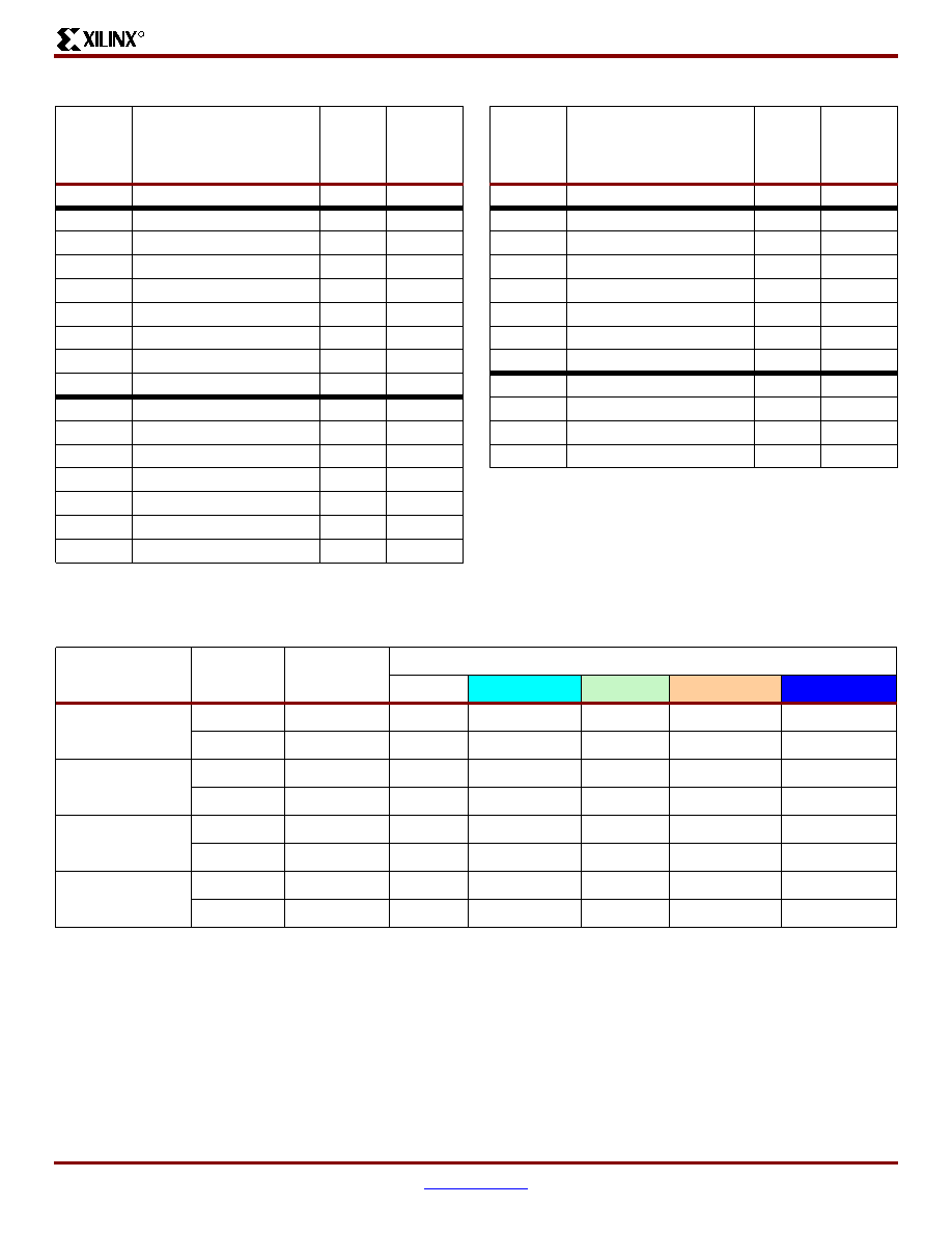
Spartan-3 1.2V FPGA Family: Pinout Descriptions
DS099-4 (v1.2.2) October 9, 2003
www.xilinx.com
41
Advance Product Specification
1-800-255-7778
R
User I/Os by Bank
Table 24
indicates how the available user-I/O pins are dis-
tributed between the eight I/O banks on the FT256 package.
N/A
GND
T16
GND
N/A
VCCAUX
A6
VCCAUX
N/A
VCCAUX
A11
VCCAUX
N/A
VCCAUX
F1
VCCAUX
N/A
VCCAUX
F16
VCCAUX
N/A
VCCAUX
L1
VCCAUX
N/A
VCCAUX
L16
VCCAUX
N/A
VCCAUX
T6
VCCAUX
N/A
VCCAUX
T11
VCCAUX
N/A
VCCINT
D4
VCCINT
N/A
VCCINT
D13
VCCINT
N/A
VCCINT
E5
VCCINT
N/A
VCCINT
E12
VCCINT
N/A
VCCINT
M5
VCCINT
N/A
VCCINT
M12
VCCINT
N/A
VCCINT
N4
VCCINT
Table 23: FT256 Package Pinout (Continued)
Bank
XC3S200
XC3S400
XC3S1000
Pin Name
FT256
Pin
Number
Type
N/A
VCCINT
N13
VCCINT
VCCAUX
CCLK
T15
CONFIG
VCCAUX
DONE
R14
CONFIG
VCCAUX
HSWAP_EN
C4
CONFIG
VCCAUX
M0
P3
CONFIG
VCCAUX
M1
T2
CONFIG
VCCAUX
M2
P4
CONFIG
VCCAUX
PROG_B
B3
CONFIG
VCCAUX
TCK
C14
JTAG
VCCAUX
TDI
A2
JTAG
VCCAUX
TDO
A15
JTAG
VCCAUX
TMS
C13
JTAG
Table 23: FT256 Package Pinout (Continued)
Bank
XC3S200
XC3S400
XC3S1000
Pin Name
FT256
Pin
Number
Type
Table 24: User I/Os Per Bank in FT256 Package
Package Edge
I/O Bank
Maximum
I/O
All Possible I/O Pins by Type
I/O
DUAL
DCI
VREF
GCLK
Top
0
20
13
0
2
3
2
1
20
13
0
2
3
2
Right
2
23
18
0
2
3
0
3
23
18
0
2
3
0
Bottom
4
21
8
6
2
3
2
5
20
7
6
2
3
2
Left
6
23
18
0
2
3
0
7
23
18
0
2
3
0
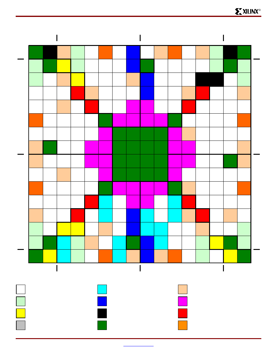
Spartan-3 1.2V FPGA Family: Pinout Descriptions
42
www.xilinx.com
DS099-4 (v1.2.2) October 9, 2003
1-800-255-7778
Advance Product Specification
R
FT256 Footprint
Figure 11: FT256 Package Footprint (top view)
113
I/O: Unrestricted, general-purpose user I/O
12
DUAL: Configuration pin, then possible
user I/O
24
VREF: User I/O or input voltage reference for
bank
16
DCI: User I/O or reference resistor input for
bank
8
GCLK: User I/O or global clock buffer input
24
VCCO: Output voltage supply for bank
7
CONFIG: Dedicated configuration pins
4
JTAG: Dedicated JTAG port pins
8
VCCINT: Internal core voltage supply
(+1.2V)
0
N.C.: No unconnected pins in this package
32
GND: Ground
8
VCCAUX: Auxiliary voltage supply
(+2.5V)
10
11
12
13
14
15
16
1
2
3
4
5
6
7
8
9
A
B
C
D
E
F
G
H
J
K
L
M
N
P
R
T
Bank 6
Bank 3
Bank 5
Bank 4
Bank 7
Bank 0
Bank 1
Bank 2
2
2
3
3
TDI
IO
VREF_0
I/O
L01P_0
VRN_0
I/O
VCCAUX
I/O
I/O
L32P_0
GCLK6
I/O
I/O
L31N_1
VREF_1
VCCAUX
I/O
I/O
L10N_1
VREF_1
I/O
L01N_1
VRP_1
TDO
I/O
L01P_7
VRN_7
PROG_B
I/O
L01N_0
VRP_0
I/O
L25P_0
I/O
L28P_0
I/O
L30P_0
I/O
L32N_0
GCLK7
I/O
L31P_1
I/O
L29N_1
I/O
L27N_1
I/O
L10P_1
I/O
L01P_1
VRN_1
I/O
L01N_2
VRP_2
I/O
L01N_7
VRP_7
I/O
L16N_7
I/O
L16P_7
VREF_7
HSWAP_
EN
I/O
L25N_0
I/O
L28N_0
I/O
L30N_0
I/O
L31P_0
VREF_0
I/O
L32N_1
GCLK5
I/O
I/O
L29P_1
I/O
L27P_1
TMS
TCK
I/O
L16N_2
I/O
L01P_2
VRN_2
I/O
L17N_7
I/O
L17P_7
I/O
L19P_7
VCCINT
IO
VREF_0
I/O
L27P_0
I/O
L29P_0
I/O
L31N_0
I/O
L32P_1
GCLK4
I/O
L30N_1
I/O
L28N_1
IO
VREF_1
VCCINT
I/O
L16P_2
I/O
L17N_2
I/O
L17P_2
VREF_2
I/O
L20N_7
I/O
L20P_7
I/O
L19N_7
VREF_7
I/O
L21P_7
VCCINT
I/O
L27N_0
I/O
L29N_0
VCCO_0 VCCO_1
I/O
L30P_1
I/O
L28P_1
VCCINT
I/O
L19N_2
I/O
L19P_2
I/O
L20N_2
I/O
L20P_2
VCCAUX
I/O
L22N_7
I/O
L22P_7
I/O
L21N_7
I/O
L23P_7
VCCO_0 VCCO_0 VCCO_1 VCCO_1
I/O
L21N_2
I/O
L21P_2
I/O
L22N_2
I/O
L22P_2
VCCAUX
I/O
L40P_7
I/O
I/O
L24N_7
I/O
L24P_7
I/O
L23N_7
VCCO_7
VCCO_2
I/O
L23N_2
VREF_2
I/O
L23P_2
I/O
L24N_2
I/O
L24P_2
I/O
I/O
L40N_7
VREF_7
I/O
L39N_7
I/O
L39P_7
VCCO_7 VCCO_7
GND
GND
GND
GND
GND
GND
GND
GND
GND
GND
GND
GND
GND
GND
GND
GND
GND
GND
GND
GND
GND
GND
GND
GND
GND
GND
GND
GND
GND
GND
VCCO_2 VCCO_2
I/O
L39N_2
I/O
L39P_2
I/O
L40N_2
I/O
L40P_2
VREF_2
I/O
L40P_6
VREF_6
I/O
L40N_6
I/O
L39P_6
I/O
L39N_6
VCCO_6 VCCO_6
VCCO_3 VCCO_3
I/O
L39P_3
I/O
L39N_3
I/O
L40N_3
VREF_3
I/O
I/O
L24P_6
I/O
L24N_6
VREF_6
I/O
L23P_6
I/O
L23N_6
VCCO_6
VCCO_3
I/O
L23N_3
I/O
L24P_3
I/O
L24N_3
I/O
I/O
L40P_3
VCCAUX
I/O
L22P_6
I/O
L22N_6
I/O
L21P_6
I/O
L21N_6
VCCO_5 VCCO_5 VCCO_4 VCCO_4
I/O
L23P_3
VREF_3
I/O
L21N_3
I/O
L22P_3
I/O
L22N_3
VCCAUX
I/O
L20P_6
I/O
L20N_6
I/O
L19P_6
I/O
L19N_6
VCCINT
I/O
L28P_5
D7
I/O
L30P_5
VCCO_5 VCCO_4
I/O
L29N_4
I/O
L27N_4
DIN
D0
VCCINT
I/O
L21P_3
I/O
L19N_3
I/O
L20P_3
I/O
L20N_3
I/O
L17P_6
VREF_6
I/O
L17N_6
I/O
L16P_6
VCCINT
I/O
I/O
L28N_5
D6
I/O
L30N_5
I/O
L32P_5
GCLK2
I/O
L31N_4
INIT_B
I/O
L29P_4
I/O
L27P_4
D1
IO
VREF_4
VCCINT
I/O
L19P_3
I/O
L17P_3
VREF_3
I/O
L17N_3
I/O
L01P_6
VRN_6
I/O
L16N_6
M0
M2
I/O
L27P_5
I/O
L29P_5
VREF_5
I/O
I/O
L32N_5
GCLK3
I/O
L31P_4
DOUT
BUSY
I/O
L30N_4
D2
I/O
L28N_4
I/O
L25N_4
IO
VREF_4
I/O
L16P_3
I/O
L16N_3
I/O
L01N_3
VRP_3
I/O
L01N_6
VRP_6
I/O
L01P_5
CS_B
I/O
L10P_5
VRN_5
I/O
L27N_5
VREF_5
I/O
L29N_5
I/O
L31P_5
D5
I/O
L32N_4
GCLK1
I/O
L30P_4
D3
I/O
L28P_4
I/O
L25P_4
I/O
L01N_4
VRP_4
DONE
GND
I/O
L01P_3
VRN_3
M1
I/O
L01N_5
RDWR_B
I/O
L10N_5
VRP_5
I/O
VCCAUX
I/O
L31N_5
D4
IO
VREF_5
I/O
L32P_4
GCLK0
IO
VREF_4
VCCAUX
I/O
I/O
L01P_4
VRN_4
I/O
CCLK
GND
DS099-4_10_030503
Spartan-3 1.2V FPGA Family: Pinout Descriptions
DS099-4 (v1.2.2) October 9, 2003
www.xilinx.com
43
Advance Product Specification
1-800-255-7778
R
FG456: 456-lead Fine-pitch Ball Grid
Array
The 456-lead fine-pitch ball grid array package, FG456,
supports three different Spartan-3 devices, including the
XC3S400, the XC3S1000, and the XC3S1500. The foot-
prints for the XC3S1000 and XC3S1500 are identical, as
shown in
Table 25
and
Figure 12
. The XC3S400, however,
has fewer I/O pins which consequently results in 69 uncon-
nected pins on the FG456 package, labeled as "N.C." In
Table 25
and
Figure 12
, these unconnected pins are indi-
cated with a black diamond symbol (
).
All the package pins appear in
Table 25
and are sorted by
bank number, then by pin name. Pairs of pins that form a dif-
ferential I/O pair appear together in the table. The table also
shows the pin number for each pin and the pin type, as
defined earlier.
If there is a difference between the XC3S400 pinout and the
pinout for the XC3S1000 and XC3S1500, then that differ-
ence is highlighted in
Table 25
. If the table entry is shaded
grey, then there is an unconnected pin on the XC3S400 that
maps to a user-I/O pin on the XC3S1000 and XC3S1500. If
the table entry is shaded tan, then the unconnected pin on
the XC3S400 maps to a VREF-type pin on the XC3S1000
and XC3S1500. If the other VREF pins in the bank all con-
nect to a voltage reference to support a special I/O stan-
dard, then also connect the N.C. pin on the XC3S400 to the
same VREF voltage. This provides maximum flexibility as
you could potentially migrate a design from the XC3S400
device to an XC3S1000 or XC3S1500 FPGA without chang-
ing the printed circuit board.
Pinout Table
Table 25: FG456 Package Pinout
Bank
3S400
Pin Name
3S1000
3S1500
Pin Name
FG456
Pin
Number
Type
0
IO
IO
A10
I/O
0
IO
IO
D9
I/O
0
IO
IO
D10
I/O
0
IO
IO
F6
I/O
0
IO/VREF_0
IO/VREF_0
A3
VREF
0
IO/VREF_0
IO/VREF_0
C7
VREF
0
N.C. (
)
IO/VREF_0
E5
VREF
0
IO/VREF_0
IO/VREF_0
F7
VREF
0
IO_L01N_0/
VRP_0
IO_L01N_0/
VRP_0
B4
DCI
0
IO_L01P_0/
VRN_0
IO_L01P_0/
VRN_0
A4
DCI
0
IO_L06N_0
IO_L06N_0
D5
I/O
0
IO_L06P_0
IO_L06P_0
C5
I/O
0
IO_L09N_0
IO_L09N_0
B5
I/O
0
IO_L09P_0
IO_L09P_0
A5
I/O
0
IO_L10N_0
IO_L10N_0
E6
I/O
0
IO_L10P_0
IO_L10P_0
D6
I/O
0
IO_L15N_0
IO_L15N_0
C6
I/O
0
IO_L15P_0
IO_L15P_0
B6
I/O
0
IO_L16N_0
IO_L16N_0
E7
I/O
0
IO_L16P_0
IO_L16P_0
D7
I/O
0
N.C. (
)
IO_L19N_0
B7
I/O
0
N.C. (
)
IO_L19P_0
A7
I/O
0
N.C. (
)
IO_L22N_0
E8
I/O
0
N.C. (
)
IO_L22P_0
D8
I/O
0
IO_L24N_0
IO_L24N_0
B8
I/O
0
IO_L24P_0
IO_L24P_0
A8
I/O
0
IO_L25N_0
IO_L25N_0
F9
I/O
0
IO_L25P_0
IO_L25P_0
E9
I/O
0
IO_L27N_0
IO_L27N_0
B9
I/O
0
IO_L27P_0
IO_L27P_0
A9
I/O
0
IO_L28N_0
IO_L28N_0
F10
I/O
0
IO_L28P_0
IO_L28P_0
E10
I/O
0
IO_L29N_0
IO_L29N_0
C10
I/O
0
IO_L29P_0
IO_L29P_0
B10
I/O
0
IO_L30N_0
IO_L30N_0
F11
I/O
0
IO_L30P_0
IO_L30P_0
E11
I/O
0
IO_L31N_0
IO_L31N_0
D11
I/O
0
IO_L31P_0/
VREF_0
IO_L31P_0/
VREF_0
C11
VREF
0
IO_L32N_0/
GCLK7
IO_L32N_0/
GCLK7
B11
GCLK
0
IO_L32P_0/
GCLK6
IO_L32P_0/
GCLK6
A11
GCLK
0
VCCO_0
VCCO_0
C8
VCCO
0
VCCO_0
VCCO_0
F8
VCCO
0
VCCO_0
VCCO_0
G9
VCCO
0
VCCO_0
VCCO_0
G10
VCCO
0
VCCO_0
VCCO_0
G11
VCCO
1
IO
IO
A12
I/O
1
IO
IO
E16
I/O
1
IO
IO
F12
I/O
1
IO
IO
F13
I/O
1
IO
IO
F16
I/O
1
IO
IO
F17
I/O
1
IO/VREF_1
IO/VREF_1
E13
VREF
1
N.C. (
)
IO/VREF_1
F14
VREF
1
IO_L01N_1/
VRP_1
IO_L01N_1/
VRP_1
C19
DCI
1
IO_L01P_1/
VRN_1
IO_L01P_1/
VRN_1
B20
DCI
Table 25: FG456 Package Pinout (Continued)
Bank
3S400
Pin Name
3S1000
3S1500
Pin Name
FG456
Pin
Number
Type
Spartan-3 1.2V FPGA Family: Pinout Descriptions
44
www.xilinx.com
DS099-4 (v1.2.2) October 9, 2003
1-800-255-7778
Advance Product Specification
R
1
IO_L06N_1/
VREF_1
IO_L06N_1/
VREF_1
A19
VREF
1
IO_L06P_1
IO_L06P_1
B19
I/O
1
IO_L09N_1
IO_L09N_1
C18
I/O
1
IO_L09P_1
IO_L09P_1
D18
I/O
1
IO_L10N_1/
VREF_1
IO_L10N_1/
VREF_1
A18
VREF
1
IO_L10P_1
IO_L10P_1
B18
I/O
1
IO_L15N_1
IO_L15N_1
D17
I/O
1
IO_L15P_1
IO_L15P_1
E17
I/O
1
IO_L16N_1
IO_L16N_1
B17
I/O
1
IO_L16P_1
IO_L16P_1
C17
I/O
1
N.C. (
)
IO_L19N_1
C16
I/O
1
N.C. (
)
IO_L19P_1
D16
I/O
1
N.C. (
)
IO_L22N_1
A16
I/O
1
N.C. (
)
IO_L22P_1
B16
I/O
1
IO_L24N_1
IO_L24N_1
D15
I/O
1
IO_L24P_1
IO_L24P_1
E15
I/O
1
IO_L25N_1
IO_L25N_1
B15
I/O
1
IO_L25P_1
IO_L25P_1
A15
I/O
1
IO_L27N_1
IO_L27N_1
D14
I/O
1
IO_L27P_1
IO_L27P_1
E14
I/O
1
IO_L28N_1
IO_L28N_1
A14
I/O
1
IO_L28P_1
IO_L28P_1
B14
I/O
1
IO_L29N_1
IO_L29N_1
C13
I/O
1
IO_L29P_1
IO_L29P_1
D13
I/O
1
IO_L30N_1
IO_L30N_1
A13
I/O
1
IO_L30P_1
IO_L30P_1
B13
I/O
1
IO_L31N_1/
VREF_1
IO_L31N_1/
VREF_1
D12
VREF
1
IO_L31P_1
IO_L31P_1
E12
I/O
1
IO_L32N_1/
GCLK5
IO_L32N_1/
GCLK5
B12
GCLK
1
IO_L32P_1/
GCLK4
IO_L32P_1/
GCLK4
C12
GCLK
1
VCCO_1
VCCO_1
C15
VCCO
1
VCCO_1
VCCO_1
F15
VCCO
1
VCCO_1
VCCO_1
G12
VCCO
1
VCCO_1
VCCO_1
G13
VCCO
1
VCCO_1
VCCO_1
G14
VCCO
2
IO
IO
C22
I/O
2
IO_L01N_2/
VRP_2
IO_L01N_2/
VRP_2
C20
DCI
2
IO_L01P_2/
VRN_2
IO_L01P_2/
VRN_2
C21
DCI
2
IO_L16N_2
IO_L16N_2
D20
I/O
Table 25: FG456 Package Pinout (Continued)
Bank
3S400
Pin Name
3S1000
3S1500
Pin Name
FG456
Pin
Number
Type
2
IO_L16P_2
IO_L16P_2
D19
I/O
2
IO_L17N_2
IO_L17N_2
D21
I/O
2
IO_L17P_2
/VREF_2
IO_L17P_2/
VREF_2
D22
VREF
2
IO_L19N_2
IO_L19N_2
E18
I/O
2
IO_L19P_2
IO_L19P_2
F18
I/O
2
IO_L20N_2
IO_L20N_2
E19
I/O
2
IO_L20P_2
IO_L20P_2
E20
I/O
2
IO_L21N_2
IO_L21N_2
E21
I/O
2
IO_L21P_2
IO_L21P_2
E22
I/O
2
IO_L22N_2
IO_L22N_2
G17
I/O
2
IO_L22P_2
IO_L22P_2
G18
I/O
2
IO_L23N_2
/VREF_2
IO_L23N_2/
VREF_2
F19
VREF
2
IO_L23P_2
IO_L23P_2
G19
I/O
2
IO_L24N_2
IO_L24N_2
F20
I/O
2
IO_L24P_2
IO_L24P_2
F21
I/O
2
N.C. (
)
IO_L26N_2
G20
I/O
2
N.C. (
)
IO_L26P_2
H19
I/O
2
IO_L27N_2
IO_L27N_2
G21
I/O
2
IO_L27P_2
IO_L27P_2
G22
I/O
2
N.C. (
)
IO_L28N_2
H18
I/O
2
N.C. (
)
IO_L28P_2
J17
I/O
2
N.C. (
)
IO_L29N_2
H21
I/O
2
N.C. (
)
IO_L29P_2
H22
I/O
2
N.C. (
)
IO_L31N_2
J18
I/O
2
N.C. (
)
IO_L31P_2
J19
I/O
2
N.C. (
)
IO_L32N_2
J21
I/O
2
N.C. (
)
IO_L32P_2
J22
I/O
2
N.C. (
)
IO_L33N_2
K17
I/O
2
N.C. (
)
IO_L33P_2
K18
I/O
2
IO_L34N_2/
VREF_2
IO_L34N_2/
VREF_2
K19
VREF
2
IO_L34P_2
IO_L34P_2
K20
I/O
2
IO_L35N_2
IO_L35N_2
K21
I/O
2
IO_L35P_2
IO_L35P_2
K22
I/O
2
IO_L38N_2
IO_L38N_2
L17
I/O
2
IO_L38P_2
IO_L38P_2
L18
I/O
2
IO_L39N_2
IO_L39N_2
L19
I/O
2
IO_L39P_2
IO_L39P_2
L20
I/O
2
IO_L40N_2
IO_L40N_2
L21
I/O
2
IO_L40P_2/
VREF_2
IO_L40P_2/
VREF_2
L22
VREF
2
VCCO_2
VCCO_2
H17
VCCO
2
VCCO_2
VCCO_2
H20
VCCO
Table 25: FG456 Package Pinout (Continued)
Bank
3S400
Pin Name
3S1000
3S1500
Pin Name
FG456
Pin
Number
Type
Spartan-3 1.2V FPGA Family: Pinout Descriptions
DS099-4 (v1.2.2) October 9, 2003
www.xilinx.com
45
Advance Product Specification
1-800-255-7778
R
2
VCCO_2
VCCO_2
J16
VCCO
2
VCCO_2
VCCO_2
K16
VCCO
2
VCCO_2
VCCO_2
L16
VCCO
3
IO
IO
Y21
I/O
3
IO_L01N_3/
VRP_3
IO_L01N_3/
VRP_3
Y20
DCI
3
IO_L01P_3/
VRN_3
IO_L01P_3/
VRN_3
Y19
DCI
3
IO_L16N_3
IO_L16N_3
W22
I/O
3
IO_L16P_3
IO_L16P_3
Y22
I/O
3
IO_L17N_3
IO_L17N_3
V19
I/O
3
IO_L17P_3/
VREF_3
IO_L17P_3/
VREF_3
W19
VREF
3
IO_L19N_3
IO_L19N_3
W21
I/O
3
IO_L19P_3
IO_L19P_3
W20
I/O
3
IO_L20N_3
IO_L20N_3
U19
I/O
3
IO_L20P_3
IO_L20P_3
V20
I/O
3
IO_L21N_3
IO_L21N_3
V22
I/O
3
IO_L21P_3
IO_L21P_3
V21
I/O
3
IO_L22N_3
IO_L22N_3
T17
I/O
3
IO_L22P_3
IO_L22P_3
U18
I/O
3
IO_L23N_3
IO_L23N_3
U21
I/O
3
IO_L23P_3/
VREF_3
IO_L23P_3/
VREF_3
U20
VREF
3
IO_L24N_3
IO_L24N_3
R18
I/O
3
IO_L24P_3
IO_L24P_3
T18
I/O
3
N.C. (
)
IO_L26N_3
T20
I/O
3
N.C. (
)
IO_L26P_3
T19
I/O
3
IO_L27N_3
IO_L27N_3
T22
I/O
3
IO_L27P_3
IO_L27P_3
T21
I/O
3
N.C. (
)
IO_L28N_3
R22
I/O
3
N.C. (
)
IO_L28P_3
R21
I/O
3
N.C. (
)
IO_L29N_3
P19
I/O
3
N.C. (
)
IO_L29P_3
R19
I/O
3
N.C. (
)
IO_L31N_3
P18
I/O
3
N.C. (
)
IO_L31P_3
P17
I/O
3
N.C. (
)
IO_L32N_3
P22
I/O
3
N.C. (
)
IO_L32P_3
P21
I/O
3
N.C. (
)
IO_L33N_3
N18
I/O
3
N.C. (
)
IO_L33P_3
N17
I/O
3
IO_L34N_3
IO_L34N_3
N20
I/O
3
IO_L34P_3/
VREF_3
IO_L34P_3/
VREF_3
N19
VREF
3
IO_L35N_3
IO_L35N_3
N22
I/O
3
IO_L35P_3
IO_L35P_3
N21
I/O
3
IO_L38N_3
IO_L38N_3
M18
I/O
Table 25: FG456 Package Pinout (Continued)
Bank
3S400
Pin Name
3S1000
3S1500
Pin Name
FG456
Pin
Number
Type
3
IO_L38P_3
IO_L38P_3
M17
I/O
3
IO_L39N_3
IO_L39N_3
M20
I/O
3
IO_L39P_3
IO_L39P_3
M19
I/O
3
IO_L40N_3/
VREF_3
IO_L40N_3/
VREF_3
M22
VREF
3
IO_L40P_3
IO_L40P_3
M21
I/O
3
VCCO_3
VCCO_3
M16
VCCO
3
VCCO_3
VCCO_3
N16
VCCO
3
VCCO_3
VCCO_3
P16
VCCO
3
VCCO_3
VCCO_3
R17
VCCO
3
VCCO_3
VCCO_3
R20
VCCO
4
IO
IO
U16
I/O
4
IO
IO
U17
I/O
4
IO
IO
W13
I/O
4
IO
IO
W14
I/O
4
IO/VREF_4
IO/VREF_4
AB13
VREF
4
IO/VREF_4
IO/VREF_4
V18
VREF
4
IO/VREF_4
IO/VREF_4
Y16
VREF
4
IO_L01N_4/
VRP_4
IO_L01N_4/
VRP_4
AA20
DCI
4
IO_L01P_4/
VRN_4
IO_L01P_4/
VRN_4
AB20
DCI
4
N.C. (
)
IO_L05N_4
AA19
I/O
4
N.C. (
)
IO_L05P_4
AB19
I/O
4
IO_L06N_4/
VREF_4
IO_L06N_4/
VREF_4
W18
VREF
4
IO_L06P_4
IO_L06P_4
Y18
I/O
4
IO_L09N_4
IO_L09N_4
AA18
I/O
4
IO_L09P_4
IO_L09P_4
AB18
I/O
4
IO_L10N_4
IO_L10N_4
V17
I/O
4
IO_L10P_4
IO_L10P_4
W17
I/O
4
IO_L15N_4
IO_L15N_4
Y17
I/O
4
IO_L15P_4
IO_L15P_4
AA17
I/O
4
IO_L16N_4
IO_L16N_4
V16
I/O
4
IO_L16P_4
IO_L16P_4
W16
I/O
4
N.C. (
)
IO_L19N_4
AA16
I/O
4
N.C. (
)
IO_L19P_4
AB16
I/O
4
N.C. (
)
IO_L22N_4/
VREF_4
V15
VREF
4
N.C. (
)
IO_L22P_4
W15
I/O
4
IO_L24N_4
IO_L24N_4
AA15
I/O
4
IO_L24P_4
IO_L24P_4
AB15
I/O
4
IO_L25N_4
IO_L25N_4
U14
I/O
4
IO_L25P_4
IO_L25P_4
V14
I/O
4
IO_L27N_4/
DIN/D0
IO_L27N_4/
DIN/D0
AA14
DUAL
Table 25: FG456 Package Pinout (Continued)
Bank
3S400
Pin Name
3S1000
3S1500
Pin Name
FG456
Pin
Number
Type
Spartan-3 1.2V FPGA Family: Pinout Descriptions
46
www.xilinx.com
DS099-4 (v1.2.2) October 9, 2003
1-800-255-7778
Advance Product Specification
R
4
IO_L27P_4/
D1
IO_L27P_4/
D1
AB14
DUAL
4
IO_L28N_4
IO_L28N_4
U13
I/O
4
IO_L28P_4
IO_L28P_4
V13
I/O
4
IO_L29N_4
IO_L29N_4
Y13
I/O
4
IO_L29P_4
IO_L29P_4
AA13
I/O
4
IO_L30N_4/
D2
IO_L30N_4/
D2
U12
DUAL
4
IO_L30P_4/
D3
IO_L30P_4/
D3
V12
DUAL
4
IO_L31N_4/
INIT_B
IO_L31N_4/
INIT_B
W12
DUAL
4
IO_L31P_4/
DOUT/BUSY
IO_L31P_4/
DOUT/BUSY
Y12
DUAL
4
IO_L32N_4/
GCLK1
IO_L32N_4/
GCLK1
AA12
GCLK
4
IO_L32P_4/
GCLK0
IO_L32P_4/
GCLK0
AB12
GCLK
4
VCCO_4
VCCO_4
T12
VCCO
4
VCCO_4
VCCO_4
T13
VCCO
4
VCCO_4
VCCO_4
T14
VCCO
4
VCCO_4
VCCO_4
U15
VCCO
4
VCCO_4
VCCO_4
Y15
VCCO
5
IO
IO
U7
I/O
5
N.C. (
)
IO
U9
I/O
5
IO
IO
U10
I/O
5
IO
IO
U11
I/O
5
IO
IO
V7
I/O
5
IO
IO
V10
I/O
5
IO/VREF_5
IO/VREF_5
AB11
VREF
5
IO/VREF_5
IO/VREF_5
U6
VREF
5
IO_L01N_5/
RDWR_B
IO_L01N_5/
RDWR_B
Y4
DUAL
5
IO_L01P_5/
CS_B
IO_L01P_5/
CS_B
AA3
DUAL
5
IO_L06N_5
IO_L06N_5
AB4
I/O
5
IO_L06P_5
IO_L06P_5
AA4
I/O
5
IO_L09N_5
IO_L09N_5
Y5
I/O
5
IO_L09P_5
IO_L09P_5
W5
I/O
5
IO_L10N_5/
VRP_5
IO_L10N_5/
VRP_5
AB5
DCI
5
IO_L10P_5/
VRN_5
IO_L10P_5/
VRN_5
AA5
DCI
5
IO_L15N_5
IO_L15N_5
W6
I/O
5
IO_L15P_5
IO_L15P_5
V6
I/O
5
IO_L16N_5
IO_L16N_5
AA6
I/O
5
IO_L16P_5
IO_L16P_5
Y6
I/O
Table 25: FG456 Package Pinout (Continued)
Bank
3S400
Pin Name
3S1000
3S1500
Pin Name
FG456
Pin
Number
Type
5
N.C. (
)
IO_L19N_5
Y7
I/O
5
N.C. (
)
IO_L19P_5/
VREF_5
W7
VREF
5
N.C. (
)
IO_L22N_5
AB7
I/O
5
N.C. (
)
IO_L22P_5
AA7
I/O
5
IO_L24N_5
IO_L24N_5
W8
I/O
5
IO_L24P_5
IO_L24P_5
V8
I/O
5
IO_L25N_5
IO_L25N_5
AB8
I/O
5
IO_L25P_5
IO_L25P_5
AA8
I/O
5
IO_L27N_5/
VREF_5
IO_L27N_5/
VREF_5
W9
VREF
5
IO_L27P_5
IO_L27P_5
V9
I/O
5
IO_L28N_5/
D6
IO_L28N_5/
D6
AB9
DUAL
5
IO_L28P_5/
D7
IO_L28P_5/
D7
AA9
DUAL
5
IO_L29N_5
IO_L29N_5
Y10
I/O
5
IO_L29P_5/
VREF_5
IO_L29P_5/
VREF_5
W10
VREF
5
IO_L30N_5
IO_L30N_5
AB10
I/O
5
IO_L30P_5
IO_L30P_5
AA10
I/O
5
IO_L31N_5/
D4
IO_L31N_5/
D4
W11
DUAL
5
IO_L31P_5/
D5
IO_L31P_5/
D5
V11
DUAL
5
IO_L32N_5/
GCLK3
IO_L32N_5/
GCLK3
AA11
GCLK
5
IO_L32P_5/
GCLK2
IO_L32P_5/
GCLK2
Y11
GCLK
5
VCCO_5
VCCO_5
T9
VCCO
5
VCCO_5
VCCO_5
T10
VCCO
5
VCCO_5
VCCO_5
T11
VCCO
5
VCCO_5
VCCO_5
U8
VCCO
5
VCCO_5
VCCO_5
Y8
VCCO
6
IO
IO
Y1
I/O
6
IO_L01N_6/
VRP_6
IO_L01N_6/
VRP_6
Y3
DCI
6
IO_L01P_6/
VRN_6
IO_L01P_6/
VRN_6
Y2
DCI
6
IO_L16N_6
IO_L16N_6
W4
I/O
6
IO_L16P_6
IO_L16P_6
W3
I/O
6
IO_L17N_6
IO_L17N_6
W2
I/O
6
IO_L17P_6/
VREF_6
IO_L17P_6/
VREF_6
W1
VREF
6
IO_L19N_6
IO_L19N_6
V5
I/O
6
IO_L19P_6
IO_L19P_6
U5
I/O
6
IO_L20N_6
IO_L20N_6
V4
I/O
Table 25: FG456 Package Pinout (Continued)
Bank
3S400
Pin Name
3S1000
3S1500
Pin Name
FG456
Pin
Number
Type
Spartan-3 1.2V FPGA Family: Pinout Descriptions
DS099-4 (v1.2.2) October 9, 2003
www.xilinx.com
47
Advance Product Specification
1-800-255-7778
R
6
IO_L20P_6
IO_L20P_6
V3
I/O
6
IO_L21N_6
IO_L21N_6
V2
I/O
6
IO_L21P_6
IO_L21P_6
V1
I/O
6
IO_L22N_6
IO_L22N_6
T6
I/O
6
IO_L22P_6
IO_L22P_6
T5
I/O
6
IO_L23N_6
IO_L23N_6
U4
I/O
6
IO_L23P_6
IO_L23P_6
T4
I/O
6
IO_L24N_6/
VREF_6
IO_L24N_6/
VREF_6
U3
VREF
6
IO_L24P_6
IO_L24P_6
U2
I/O
6
N.C. (
)
IO_L26N_6
T3
I/O
6
N.C. (
)
IO_L26P_6
R4
I/O
6
IO_L27N_6
IO_L27N_6
T2
I/O
6
IO_L27P_6
IO_L27P_6
T1
I/O
6
N.C. (
)
IO_L28N_6
R5
I/O
6
N.C. (
)
IO_L28P_6
P6
I/O
6
N.C. (
)
IO_L29N_6
R2
I/O
6
N.C. (
)
IO_L29P_6
R1
I/O
6
N.C. (
)
IO_L31N_6
P5
I/O
6
N.C. (
)
IO_L31P_6
P4
I/O
6
N.C. (
)
IO_L32N_6
P2
I/O
6
N.C. (
)
IO_L32P_6
P1
I/O
6
N.C. (
)
IO_L33N_6
N6
I/O
6
N.C. (
)
IO_L33P_6
N5
I/O
6
IO_L34N_6/
VREF_6
IO_L34N_6/
VREF_6
N4
VREF
6
IO_L34P_6
IO_L34P_6
N3
I/O
6
IO_L35N_6
IO_L35N_6
N2
I/O
6
IO_L35P_6
IO_L35P_6
N1
I/O
6
IO_L38N_6
IO_L38N_6
M6
I/O
6
IO_L38P_6
IO_L38P_6
M5
I/O
6
IO_L39N_6
IO_L39N_6
M4
I/O
6
IO_L39P_6
IO_L39P_6
M3
I/O
6
IO_L40N_6
IO_L40N_6
M2
I/O
6
IO_L40P_6/
VREF_6
IO_L40P_6/
VREF_6
M1
VREF
6
VCCO_6
VCCO_6
M7
VCCO
6
VCCO_6
VCCO_6
N7
VCCO
6
VCCO_6
VCCO_6
P7
VCCO
6
VCCO_6
VCCO_6
R3
VCCO
6
VCCO_6
VCCO_6
R6
VCCO
7
IO
IO
C2
I/O
7
IO_L01N_7/
VRP_7
IO_L01N_7/
VRP_7
C3
DCI
7
IO_L01P_7/
VRN_7
IO_L01P_7/
VRN_7
C4
DCI
Table 25: FG456 Package Pinout (Continued)
Bank
3S400
Pin Name
3S1000
3S1500
Pin Name
FG456
Pin
Number
Type
7
IO_L16N_7
IO_L16N_7
D1
I/O
7
IO_L16P_7/
VREF_7
IO_L16P_7/
VREF_7
C1
VREF
7
IO_L17N_7
IO_L17N_7
E4
I/O
7
IO_L17P_7
IO_L17P_7
D4
I/O
7
IO_L19N_7/
VREF_7
IO_L19N_7/
VREF_7
D3
VREF
7
IO_L19P_7
IO_L19P_7
D2
I/O
7
IO_L20N_7
IO_L20N_7
F4
I/O
7
IO_L20P_7
IO_L20P_7
E3
I/O
7
IO_L21N_7
IO_L21N_7
E1
I/O
7
IO_L21P_7
IO_L21P_7
E2
I/O
7
IO_L22N_7
IO_L22N_7
G6
I/O
7
IO_L22P_7
IO_L22P_7
F5
I/O
7
IO_L23N_7
IO_L23N_7
F2
I/O
7
IO_L23P_7
IO_L23P_7
F3
I/O
7
IO_L24N_7
IO_L24N_7
H5
I/O
7
IO_L24P_7
IO_L24P_7
G5
I/O
7
N.C. (
)
IO_L26N_7
G3
I/O
7
N.C. (
)
IO_L26P_7
G4
I/O
7
IO_L27N_7
IO_L27N_7
G1
I/O
7
IO_L27P_7/
VREF_7
IO_L27P_7/
VREF_7
G2
VREF
7
N.C. (
)
IO_L28N_7
H1
I/O
7
N.C. (
)
IO_L28P_7
H2
I/O
7
N.C. (
)
IO_L29N_7
J4
I/O
7
N.C. (
)
IO_L29P_7
H4
I/O
7
N.C. (
)
IO_L31N_7
J5
I/O
7
N.C. (
)
IO_L31P_7
J6
I/O
7
N.C. (
)
IO_L32N_7
J1
I/O
7
N.C. (
)
IO_L32P_7
J2
I/O
7
N.C. (
)
IO_L33N_7
K5
I/O
7
N.C. (
)
IO_L33P_7
K6
I/O
7
IO_L34N_7
IO_L34N_7
K3
I/O
7
IO_L34P_7
IO_L34P_7
K4
I/O
7
IO_L35N_7
IO_L35N_7
K1
I/O
7
IO_L35P_7
IO_L35P_7
K2
I/O
7
IO_L38N_7
IO_L38N_7
L5
I/O
7
IO_L38P_7
IO_L38P_7
L6
I/O
7
IO_L39N_7
IO_L39N_7
L3
I/O
7
IO_L39P_7
IO_L39P_7
L4
I/O
7
IO_L40N_7/
VREF_7
IO_L40N_7/
VREF_7
L1
VREF
7
IO_L40P_7
IO_L40P_7
L2
I/O
7
VCCO_7
VCCO_7
H3
VCCO
7
VCCO_7
VCCO_7
H6
VCCO
Table 25: FG456 Package Pinout (Continued)
Bank
3S400
Pin Name
3S1000
3S1500
Pin Name
FG456
Pin
Number
Type
Spartan-3 1.2V FPGA Family: Pinout Descriptions
48
www.xilinx.com
DS099-4 (v1.2.2) October 9, 2003
1-800-255-7778
Advance Product Specification
R
7
VCCO_7
VCCO_7
J7
VCCO
7
VCCO_7
VCCO_7
K7
VCCO
7
VCCO_7
VCCO_7
L7
VCCO
N/A
GND
GND
A1
GND
N/A
GND
GND
A22
GND
N/A
GND
GND
AA2
GND
N/A
GND
GND
AA21
GND
N/A
GND
GND
AB1
GND
N/A
GND
GND
AB22
GND
N/A
GND
GND
B2
GND
N/A
GND
GND
B21
GND
N/A
GND
GND
C9
GND
N/A
GND
GND
C14
GND
N/A
GND
GND
J3
GND
N/A
GND
GND
J9
GND
N/A
GND
GND
J10
GND
N/A
GND
GND
J11
GND
N/A
GND
GND
J12
GND
N/A
GND
GND
J13
GND
N/A
GND
GND
J14
GND
N/A
GND
GND
J20
GND
N/A
GND
GND
K9
GND
N/A
GND
GND
K10
GND
N/A
GND
GND
K11
GND
N/A
GND
GND
K12
GND
N/A
GND
GND
K13
GND
N/A
GND
GND
K14
GND
N/A
GND
GND
L9
GND
N/A
GND
GND
L10
GND
N/A
GND
GND
L11
GND
N/A
GND
GND
L12
GND
N/A
GND
GND
L13
GND
N/A
GND
GND
L14
GND
N/A
GND
GND
M9
GND
N/A
GND
GND
M10
GND
N/A
GND
GND
M11
GND
N/A
GND
GND
M12
GND
N/A
GND
GND
M13
GND
N/A
GND
GND
M14
GND
N/A
GND
GND
N9
GND
N/A
GND
GND
N10
GND
N/A
GND
GND
N11
GND
N/A
GND
GND
N12
GND
N/A
GND
GND
N13
GND
N/A
GND
GND
N14
GND
Table 25: FG456 Package Pinout (Continued)
Bank
3S400
Pin Name
3S1000
3S1500
Pin Name
FG456
Pin
Number
Type
N/A
GND
GND
P3
GND
N/A
GND
GND
P9
GND
N/A
GND
GND
P10
GND
N/A
GND
GND
P11
GND
N/A
GND
GND
P12
GND
N/A
GND
GND
P13
GND
N/A
GND
GND
P14
GND
N/A
GND
GND
P20
GND
N/A
GND
GND
Y9
GND
N/A
GND
GND
Y14
GND
N/A
VCCAUX
VCCAUX
A6
VCCAUX
N/A
VCCAUX
VCCAUX
A17
VCCAUX
N/A
VCCAUX
VCCAUX
AB6
VCCAUX
N/A
VCCAUX
VCCAUX
AB17
VCCAUX
N/A
VCCAUX
VCCAUX
F1
VCCAUX
N/A
VCCAUX
VCCAUX
F22
VCCAUX
N/A
VCCAUX
VCCAUX
U1
VCCAUX
N/A
VCCAUX
VCCAUX
U22
VCCAUX
N/A
VCCINT
VCCINT
G7
VCCINT
N/A
VCCINT
VCCINT
G8
VCCINT
N/A
VCCINT
VCCINT
G15
VCCINT
N/A
VCCINT
VCCINT
G16
VCCINT
N/A
VCCINT
VCCINT
H7
VCCINT
N/A
VCCINT
VCCINT
H16
VCCINT
N/A
VCCINT
VCCINT
R7
VCCINT
N/A
VCCINT
VCCINT
R16
VCCINT
N/A
VCCINT
VCCINT
T7
VCCINT
N/A
VCCINT
VCCINT
T8
VCCINT
N/A
VCCINT
VCCINT
T15
VCCINT
N/A
VCCINT
VCCINT
T16
VCCINT
VCCAUX CCLK
CCLK
AA22
CONFIG
VCCAUX DONE
DONE
AB21
CONFIG
VCCAUX HSWAP_EN
HSWAP_EN
B3
CONFIG
VCCAUX M0
M0
AB2
CONFIG
VCCAUX M1
M1
AA1
CONFIG
VCCAUX M2
M2
AB3
CONFIG
VCCAUX PROG_B
PROG_B
A2
CONFIG
VCCAUX TCK
TCK
A21
JTAG
VCCAUX TDI
TDI
B1
JTAG
VCCAUX TDO
TDO
B22
JTAG
VCCAUX TMS
TMS
A20
JTAG
Table 25: FG456 Package Pinout (Continued)
Bank
3S400
Pin Name
3S1000
3S1500
Pin Name
FG456
Pin
Number
Type

Spartan-3 1.2V FPGA Family: Pinout Descriptions
DS099-4 (v1.2.2) October 9, 2003
www.xilinx.com
49
Advance Product Specification
1-800-255-7778
R
User I/Os by Bank
Table 26
indicates how the available user-I/O pins are dis-
tributed between the eight I/O banks for the XC3S400 in the
FG456 package. Similarly,
Table 27
shows how the avail-
able user-I/O pins are distributed between the eight I/O
banks for the XC3S1000 and XC3S1500 in the FG456
package.
Table 26: User I/Os Per Bank for XC3S400 in FG456 Package
Edge
I/O
Bank
Maximum
I/O
All Possible I/O Pins by Type
I/O
DUAL
DCI
VREF
GCLK
Top
0
35
27
0
2
4
2
1
35
27
0
2
4
2
Right
2
31
25
0
2
4
0
3
31
25
0
2
4
0
Bottom
4
35
21
6
2
4
2
5
35
21
6
2
4
2
Left
6
31
25
0
2
4
0
7
31
25
0
2
4
0
Table 27: User I/Os Per Bank for XC3S1000 and XC3S1500 in FG456 Package
Edge
I/O Bank
Maximum
I/O
All Possible I/O Pins by Type
I/O
DUAL
DCI
VREF
GCLK
Top
0
40
31
0
2
5
2
1
40
31
0
2
5
2
Right
2
43
37
0
2
4
0
3
43
37
0
2
4
0
Bottom
4
41
26
6
2
5
2
5
40
25
6
2
5
2
Left
6
43
37
0
2
4
0
7
43
37
0
2
4
0
Spartan-3 1.2V FPGA Family: Pinout Descriptions
50
www.xilinx.com
DS099-4 (v1.2.2) October 9, 2003
1-800-255-7778
Advance Product Specification
R
FG456 Footprint
Left Half of Package
(top view)
XC3S400
(264 max. user I/O)
196
I/O: Unrestricted,
general-purpose user I/O
32
VREF: User I/O or input
voltage reference for bank
69
N.C.: Unconnected pins for
XC3S400 (
)
XC3S1000, XC3S1500
(333 max user I/O)
261
I/O: Unrestricted,
general-purpose user I/O
36
VREF: User I/O or input
voltage reference for bank
0
N.C.: No unconnected pins
in this package
All devices
12
DUAL: Configuration pin,
then possible user I/O
8
GCLK: User I/O or global
clock buffer input
16
DCI: User I/O or reference
resistor input for bank
7
CONFIG: Dedicated
configuration pins
4
JTAG: Dedicated JTAG
port pins
12
VCCINT: Internal core
voltage supply (+1.2V)
40
VCCO: Output voltage
supply for bank
8
VCCAUX: Auxiliary voltage
supply (+2.5V)
52
GND: Ground
Figure 12: FG456 Package Footprint (top view)
Bank 5
Bank 0
A
B
C
D
E
F
G
H
J
K
L
M
N
P
R
T
U
V
W
Y
A
A
A
B
Bank 7
Bank 6
PROG_B
IO
VREF_0
I/O
L01P_0
VRN_0
I/O
L09P_0
VCCAUX
I/O
L19P_0 I/O
L24P_0
I/O
L27P_0
I/O
I/O
L32P_0
GCLK6
TDI
HSWAP_
EN
I/O
L01N_0
VRP_0
I/O
L09N_0
I/O
L15P_0
I/O
L19N_0
I/O
L24N_0
I/O
L27N_0
I/O
L29P_0
I/O
L32N_0
GCLK7
I/O
L16P_7
VREF_7
I/O
I/O
L01N_7
VRP_7
I/O
L01P_7
VRN_7
I/O
L06P_0
I/O
L15N_0
IO
VREF_0
VCCO_0
GND
GND
GND
I/O
L29N_0
I/O
L31P_0
VREF_0
I/O
L16N_7
I/O
L19P_7
I/O
L19N_7
VREF_7
I/O
L17P_7
I/O
L06N_0
I/O
L10P_0
I/O
L16P_0
I/O
L22P_0 I/O
I/O
I/O
L31N_0
I/O
L21N_7
I/O
L21P_7
I/O
L20P_7
I/O
L17N_7
IO
VREF_0 I/O
L10N_0
I/O
L16N_0
I/O
L22N_0
I/O
L25P_0
I/O
L28P_0
I/O
L30P_0
VCCAUX
I/O
L23N_7
I/O
L23P_7
I/O
L20N_7
I/O
L22P_7
I/O
IO
VREF_0
VCCO_0
I/O
L25N_0
I/O
L28N_0
I/O
L30N_0
I/O
L27N_7
I/O
L27P_7
VREF_7
I/O
L26N_7
I/O
L26P_7
I/O
L24P_7
I/O
L22N_7
VCCINT VCCINT
VCCO_0 VCCO_0 VCCO_0
I/O
L28N_7
I/O
L28P_7
VCCO_7
I/O
L29P_7 I/O
L24N_7
VCCO_7
VCCINT
I/O
L32N_7
I/O
L32P_7
GND
I/O
L29N_7
I/O
L31N_7
I/O
L31P_7
VCCO_7
I/O
L35N_7
I/O
L35P_7
I/O
L34N_7
I/O
L34P_7
I/O
L33N_7
I/O
L33P_7
VCCO_7
I/O
L40N_7
VREF_7
I/O
L40P_7
I/O
L39N_7
I/O
L39P_7
I/O
L38N_7
I/O
L38P_7
VCCO_7
I/O
L40P_6
VREF_6
I/O
L40N_6
I/O
L39P_6
I/O
L39N_6
I/O
L38P_6
I/O
L38N_6
VCCO_6
GND
GND
GND
GND
GND
GND
GND
GND
GND
GND
GND
GND
GND
GND
GND
GND
GND
GND
I/O
L35P_6
I/O
L35N_6
I/O
L34P_6
I/O
L34N_6
VREF_6
I/O
L33P_6
I/O
L33N_6
VCCO_6
I/O
L32P_6
I/O
L32N_6
GND
I/O
L31P_6
I/O
L31N_6
I/O
L28P_6
VCCO_6
I/O
L29P_6
I/O
L29N_6
VCCO_6
I/O
L26P_6
I/O
L28N_6
VCCO_6
VCCINT
I/O
L27P_6
I/O
L27N_6
I/O
L26N_6
I/O
L23P_6
I/O
L22P_6
I/O
L22N_6
VCCINT VCCINT
VCCO_5 VCCO_5 VCCO_5
VCCAUX
I/O
L24P_6
I/O
L24N_6
VREF_6
I/O
L23N_6
I/O
L19P_6
IO
VREF_5
I/O
VCCO_5
I/O
I/O
I/O
I/O
L21P_6
I/O
L21N_6
I/O
L20P_6
I/O
L20N_6
I/O
L19N_6
I/O
L15P_5
I/O
I/O
L24P_5
I/O
L27P_5
I/O
I/O
L31P_5
D5
I/O
L17P_6
VREF_6
I/O
L17N_6
I/O
L16P_6
I/O
L16N_6
I/O
L09P_5
I/O
L15N_5
I/O
L19P_5
VREF_5
I/O
L24N_5
I/O
L27N_5
VREF_5
I/O
L29P_5
VREF_5
I/O
L31N_5
D4
I/O
I/O
L01P_6
VRN_6
I/O
L01N_6
VRP_6
I/O
L01N_5
RDWR_B
I/O
L09N_5
I/O
L16P_5
I/O
L19N_5
VCCO_5
I/O
L29N_5
I/O
L32P_5
GCLK2
M1
I/O
L01P_5
CS_B
I/O
L06P_5
I/O
L10P_5
VRN_5
I/O
L16N_5
I/O
L22P_5
I/O
L25P_5
I/O
L28P_5
D7
I/O
L30P_5
I/O
L32N_5
GCLK3
GND
GND
GND
M0
M2
I/O
L06N_5
I/O
L10N_5
VRP_5
VCCAUX
I/O
L22N_5
I/O
L25N_5
I/O
L28N_5
D6
I/O
L30N_5
IO
VREF_5
DS099-4_11a_030203
10
3
4
1
2
5
6
7
8
9
11
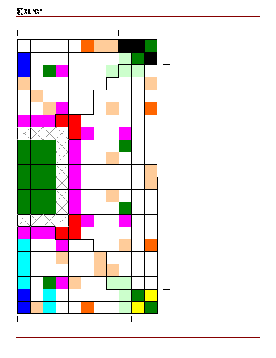
Spartan-3 1.2V FPGA Family: Pinout Descriptions
DS099-4 (v1.2.2) October 9, 2003
www.xilinx.com
51
Advance Product Specification
1-800-255-7778
R
Right Half of Package
(top view)
12
13
14
15
16
17
18
19
20
21
22
Bank 1
Bank 4
A
B
C
D
E
F
G
H
J
K
L
M
N
P
R
T
U
V
W
Y
A
A
A
B
Bank 2
Bank 3
I/O
I/O
L30N_1
I/O
L28N_1
I/O
L25P_1
I/O
L22N_1
VCCAUX
I/O
L10N_1
VREF_1
I/O
L06N_1
VREF_1
TMS
TCK
TDO
GND
I/O
L32N_1
GCLK5
I/O
L30P_1
I/O
L28P_1
I/O
L25N_1
I/O
I/O
L16N_1
I/O
L10P_1
I/O
L06P_1
I/O
L01P_1
VRN_1
GND
I/O
L32P_1
GCLK4
I/O
L29N_1
GND
VCCO_1
I/O
L19N_1
I/O
L16P_1
I/O
L09N_1
I/O
L01N_1
VRP_1
I/O
L01N_2
VRP_2
I/O
L01P_2
VRN_2
I/O
I/O
L31N_1
VREF_1
I/O
L29P_1
I/O
L27N_1
I/O
L24N_1
I/O
L19P_1 I/O
L15N_1
I/O
L09P_1
I/O
L16P_2
I/O
L16N_2
I/O
L17N_2
I/O
L17P_2
VREF_2
I/O
L31P_1
IO
VREF_1
I/O
L27P_1
I/O
L24P_1
I/O
I/O
L15P_1
I/O
L19N_2
I/O
L20N_2
I/O
L20P_2
I/O
L21N_2
I/O
L21P_2
I/O
I/O
IO
VREF_1
VCCO_1
I/O
I/O
I/O
L19P_2
I/O
L23N_2
VREF_2
I/O
L24N_2
I/O
L24P_2
VCCAUX
VCCO_1 VCCO_1 VCCO_1
VCCINT VCCINT
I/O
L22N_2
I/O
L22P_2
I/O
L23P_2
I/O
L26N_2
I/O
L27N_2
I/O
L27P_2
VCCINT
VCCO_2
I/O
L28N_2
I/O
L26P_2
VCCO_2
I/O
L29N_2
I/O
L29P_2
GND
GND
GND
VCCO_2
I/O
L28P_2
I/O
L31N_2
I/O
L31P_2
GND
I/O
L32N_2
I/O
L32P_2
GND
GND
GND
VCCO_2
I/O
L33N_2
I/O
L33P_2
I/O
L34N_2
VREF_2
I/O
L34P_2
I/O
L35N_2
I/O
L35P_2
GND
GND
GND
VCCO_2
I/O
L38N_2
I/O
L38P_2
I/O
L39N_2
I/O
L39P_2
I/O
L40N_2
I/O
L40P_2
VREF_2
GND
GND
GND
VCCO_3
I/O
L38P_3
I/O
L38N_3
I/O
L39P_3
I/O
L39N_3
I/O
L40P_3
I/O
L40N_3
VREF_3
GND
GND
GND
VCCO_3
I/O
L33P_3
I/O
L33N_3
I/O
L34P_3
VREF_3
I/O
L34N_3
I/O
L35P_3
I/O
L35N_3
GND
GND
GND
VCCO_3
I/O
L31P_3
I/O
L31N_3
I/O
L29N_3
GND
I/O
L32P_3
I/O
L32N_3
VCCINT
VCCO_3
I/O
L24N_3
I/O
L29P_3
VCCO_3
I/O
L28P_3
I/O
L28N_3
VCCO_4 VCCO_4 VCCO_4
VCCINT VCCINT
I/O
L22N_3
I/O
L24P_3
I/O
L26P_3
I/O
L26N_3
I/O
L27P_3
I/O
L27N_3
I/O
L30N_4
D2
I/O
L28N_4
I/O
L25N_4
VCCO_4
I/O
I/O
I/O
L22P_3
I/O
L20N_3
I/O
L23P_3
VREF_3
I/O
L23N_3
VCCAUX
I/O
L30P_4
D3
I/O
L28P_4
I/O
L25P_4
I/O
L22N_4
VREF_4
I/O
L16N_4
I/O
L10N_4
IO
VREF_4
I/O
L17N_3
I/O
L20P_3
I/O
L21P_3
I/O
L21N_3
I/O
L31N_4
INIT_B
I/O
I/O
I/O
L22P_4 I/O
L16P_4
I/O
L10P_4
I/O
L06N_4
VREF_4
I/O
L17P_3
VREF_3
I/O
L19P_3
I/O
L19N_3
I/O
L16N_3
I/O
L31P_4
DOUT
BUSY
I/O
L29N_4
GND
VCCO_4
IO
VREF_4
I/O
L15N_4
I/O
L06P_4
I/O
L01P_3
VRN_3
I/O
L01N_3
VRP_3
I/O
I/O
L16P_3
I/O
L32N_4
GCLK1
I/O
L29P_4
I/O
L27N_4
DIN
D0
I/O
L24N_4
I/O
L19N_4
I/O
L15P_4
I/O
L09N_4
I/O
L05N_4
I/O
L01N_4
VRP_4
GND
CCLK
I/O
L32P_4
GCLK0
IO
VREF_4
I/O
L27P_4
D1
I/O
L24P_4
I/O
L19P_4
VCCAUX
I/O
L09P_4
I/O
L05P_4
I/O
L01P_4
VRN_4
DONE
GND
DS099-4_11b_030503
L22P_1
Spartan-3 1.2V FPGA Family: Pinout Descriptions
52
www.xilinx.com
DS099-4 (v1.2.2) October 9, 2003
1-800-255-7778
Advance Product Specification
R
FG676: 676-lead Fine-pitch Ball Grid
Array
The 676-lead fine-pitch ball grid array package, FG676,
supports three different Spartan-3 devices, including the
XC3S1000, the XC3S1500, and the XC3S2000. All three
have nearly identical footprints but are slightly different due
to unconnected pins on the XC3S1000 and XC3S1500. For
example, because the XC3S1000 has fewer I/O pins, this
device has 98 unconnected pins on the FG456 package,
labeled as "N.C." In
Table 28
and
Figure 13
, these uncon-
nected pins are indicated with a black diamond symbol (
).
The XC3S1500, however, has only two unconnected pins,
also labeled "N.C." in the pinout table but indicated with a
black square symbol ( ).
All the package pins appear in
Table 28
and are sorted by
bank number, then by pin name. Pairs of pins that form a dif-
ferential I/O pair appear together in the table. The table also
shows the pin number for each pin and the pin type, as
defined earlier.
If there is a difference between the XC1000, XC3S1500 and
XC3S2000 pinouts, then that difference is highlighted in
Table 28
. If the table entry is shaded grey, then there is an
unconnected pin on either the XC3S1000 or XC3S1500 that
maps to a user-I/O pin on the XC3S2000. If the table entry
is shaded tan, then the unconnected pin on either the
XC3S1000 or XC3S1500 maps to a VREF-type pin on the
XC3S2000. If the other VREF pins in the bank all connect to
a voltage reference to support a special I/O standard, then
also connect the N.C. pin on the XC3S1000 or XC3S1500
to the same VREF voltage. This provides maximum flexibil-
ity as you could potentially migrate a design from the
XC3S1000 through to the XC3S2000 FPGA without chang-
ing the printed circuit board.
Pinout Table
Table 28: FG676 Package Pinout
Bank
XC3S1000
Pin Name
XC3S1500
Pin Name
XC3S2000
Pin Name
FG676
Pin
Number
Type
0
IO
IO
IO
A3
I/O
0
IO
IO
IO
A5
I/O
0
IO
IO
IO
A6
I/O
0
IO
IO
IO
C4
I/O
0
N.C. (
)
IO
IO
C8
I/O
0
IO
IO
IO
C12
I/O
0
IO
IO
IO
E13
I/O
0
IO
IO
IO
H11
I/O
0
IO
IO
IO
H12
I/O
0
IO/VREF_0
IO/VREF_0
IO/VREF_0
B3
VREF
0
IO/VREF_0
IO/VREF_0
IO/VREF_0
F7
VREF
0
IO/VREF_0
IO/VREF_0
IO/VREF_0
G10
VREF
0
IO_L01N_0/
VRP_0
IO_L01N_0/
VRP_0
IO_L01N_0/
VRP_0
E5
DCI
0
IO_L01P_0/
VRN_0
IO_L01P_0/
VRN_0
IO_L01P_0/
VRN_0
D5
DCI
0
IO_L05N_0
IO_L05N_0
IO_L05N_0
B4
I/O
0
IO_L05P_0/
VREF_0
IO_L05P_0/
VREF_0
IO_L05P_0/
VREF_0
A4
VREF
0
IO_L06N_0
IO_L06N_0
IO_L06N_0
C5
I/O
0
IO_L06P_0
IO_L06P_0
IO_L06P_0
B5
I/O
0
IO_L07N_0
IO_L07N_0
IO_L07N_0
E6
I/O
0
IO_L07P_0
IO_L07P_0
IO_L07P_0
D6
I/O
0
IO_L08N_0
IO_L08N_0
IO_L08N_0
C6
I/O
0
IO_L08P_0
IO_L08P_0
IO_L08P_0
B6
I/O
0
IO_L09N_0
IO_L09N_0
IO_L09N_0
E7
I/O
0
IO_L09P_0
IO_L09P_0
IO_L09P_0
D7
I/O
0
IO_L10N_0
IO_L10N_0
IO_L10N_0
B7
I/O
0
IO_L10P_0
IO_L10P_0
IO_L10P_0
A7
I/O
0
N.C. (
)
IO_L11N_0
IO_L11N_0
G8
I/O
0
N.C. (
)
IO_L11P_0
IO_L11P_0
F8
I/O
0
N.C. (
)
IO_L12N_0
IO_L12N_0
E8
I/O
0
N.C. (
)
IO_L12P_0
IO_L12P_0
D8
I/O
0
IO_L15N_0
IO_L15N_0
IO_L15N_0
B8
I/O
0
IO_L15P_0
IO_L15P_0
IO_L15P_0
A8
I/O
0
IO_L16N_0
IO_L16N_0
IO_L16N_0
G9
I/O
0
IO_L16P_0
IO_L16P_0
IO_L16P_0
F9
I/O
0
N.C. (
)
IO_L17N_0
IO_L17N_0
E9
I/O
0
N.C. (
)
IO_L17P_0
IO_L17P_0
D9
I/O
0
N.C. (
)
IO_L18N_0
IO_L18N_0
C9
I/O
0
N.C. (
)
IO_L18P_0
IO_L18P_0
B9
I/O
0
IO_L19N_0
IO_L19N_0
IO_L19N_0
F10
I/O
0
IO_L19P_0
IO_L19P_0
IO_L19P_0
E10
I/O
0
IO_L22N_0
IO_L22N_0
IO_L22N_0
D10
I/O
0
IO_L22P_0
IO_L22P_0
IO_L22P_0
C10
I/O
0
N.C. (
)
IO_L23N_0
IO_L23N_0
B10
I/O
0
N.C. (
)
IO_L23P_0
IO_L23P_0
A10
I/O
0
IO_L24N_0
IO_L24N_0
IO_L24N_0
G11
I/O
0
IO_L24P_0
IO_L24P_0
IO_L24P_0
F11
I/O
0
IO_L25N_0
IO_L25N_0
IO_L25N_0
E11
I/O
0
IO_L25P_0
IO_L25P_0
IO_L25P_0
D11
I/O
0
N.C. (
)
IO_L26N_0
IO_L26N_0
B11
I/O
0
N.C. (
)
IO_L26P_0/
VREF_0
IO_L26P_0/
VREF_0
A11
VREF
0
IO_L27N_0
IO_L27N_0
IO_L27N_0
G12
I/O
0
IO_L27P_0
IO_L27P_0
IO_L27P_0
H13
I/O
0
IO_L28N_0
IO_L28N_0
IO_L28N_0
F12
I/O
0
IO_L28P_0
IO_L28P_0
IO_L28P_0
E12
I/O
0
IO_L29N_0
IO_L29N_0
IO_L29N_0
B12
I/O
0
IO_L29P_0
IO_L29P_0
IO_L29P_0
A12
I/O
Table 28: FG676 Package Pinout (Continued)
Bank
XC3S1000
Pin Name
XC3S1500
Pin Name
XC3S2000
Pin Name
FG676
Pin
Number
Type

Spartan-3 1.2V FPGA Family: Pinout Descriptions
DS099-4 (v1.2.2) October 9, 2003
www.xilinx.com
53
Advance Product Specification
1-800-255-7778
R
0
IO_L30N_0
IO_L30N_0
IO_L30N_0
G13
I/O
0
IO_L30P_0
IO_L30P_0
IO_L30P_0
F13
I/O
0
IO_L31N_0
IO_L31N_0
IO_L31N_0
D13
I/O
0
IO_L31P_0/
VREF_0
IO_L31P_0/
VREF_0
IO_L31P_0/
VREF_0
C13
VREF
0
IO_L32N_0/
GCLK7
IO_L32N_0/
GCLK7
IO_L32N_0/
GCLK7
B13
GCLK
0
IO_L32P_0/
GCLK6
IO_L32P_0/
GCLK6
IO_L32P_0/
GCLK6
A13
GCLK
0
VCCO_0
VCCO_0
VCCO_0
C7
VCCO
0
VCCO_0
VCCO_0
VCCO_0
C11
VCCO
0
VCCO_0
VCCO_0
VCCO_0
H9
VCCO
0
VCCO_0
VCCO_0
VCCO_0
H10
VCCO
0
VCCO_0
VCCO_0
VCCO_0
J11
VCCO
0
VCCO_0
VCCO_0
VCCO_0
J12
VCCO
0
VCCO_0
VCCO_0
VCCO_0
J13
VCCO
0
VCCO_0
VCCO_0
VCCO_0
K13
VCCO
1
IO
IO
IO
A14
I/O
1
IO
IO
IO
A22
I/O
1
IO
IO
IO
A23
I/O
1
IO
IO
IO
D16
I/O
1
IO
IO
IO
E18
I/O
1
IO
IO
IO
F14
I/O
1
IO
IO
IO
F20
I/O
1
IO
IO
IO
G19
I/O
1
IO/VREF_1
IO/VREF_1
IO/VREF_1
C15
VREF
1
IO/VREF_1
IO/VREF_1
IO/VREF_1
C17
VREF
1
N.C. (
)
IO/VREF_1
IO/VREF_1
D18
VREF
1
IO_L01N_1/
VRP_1
IO_L01N_1/
VRP_1
IO_L01N_1/
VRP_1
D22
DCI
1
IO_L01P_1/
VRN_1
IO_L01P_1/
VRN_1
IO_L01P_1/
VRN_1
E22
DCI
1
IO_L04N_1
IO_L04N_1
IO_L04N_1
B23
I/O
1
IO_L04P_1
IO_L04P_1
IO_L04P_1
C23
I/O
1
IO_L05N_1
IO_L05N_1
IO_L05N_1
E21
I/O
1
IO_L05P_1
IO_L05P_1
IO_L05P_1
F21
I/O
1
IO_L06N_1/
VREF_1
IO_L06N_1/
VREF_1
IO_L06N_1/
VREF_1
B22
VREF
1
IO_L06P_1
IO_L06P_1
IO_L06P_1
C22
I/O
1
IO_L07N_1
IO_L07N_1
IO_L07N_1
C21
I/O
1
IO_L07P_1
IO_L07P_1
IO_L07P_1
D21
I/O
1
IO_L08N_1
IO_L08N_1
IO_L08N_1
A21
I/O
1
IO_L08P_1
IO_L08P_1
IO_L08P_1
B21
I/O
1
IO_L09N_1
IO_L09N_1
IO_L09N_1
D20
I/O
1
IO_L09P_1
IO_L09P_1
IO_L09P_1
E20
I/O
1
IO_L10N_1/
VREF_1
IO_L10N_1/
VREF_1
IO_L10N_1/
VREF_1
A20
VREF
Table 28: FG676 Package Pinout (Continued)
Bank
XC3S1000
Pin Name
XC3S1500
Pin Name
XC3S2000
Pin Name
FG676
Pin
Number
Type
1
IO_L10P_1
IO_L10P_1
IO_L10P_1
B20
I/O
1
N.C. (
)
IO_L11N_1
IO_L11N_1
E19
I/O
1
N.C. (
)
IO_L11P_1
IO_L11P_1
F19
I/O
1
N.C. (
)
IO_L12N_1
IO_L12N_1
C19
I/O
1
N.C. (
)
IO_L12P_1
IO_L12P_1
D19
I/O
1
IO_L15N_1
IO_L15N_1
IO_L15N_1
A19
I/O
1
IO_L15P_1
IO_L15P_1
IO_L15P_1
B19
I/O
1
IO_L16N_1
IO_L16N_1
IO_L16N_1
F18
I/O
1
IO_L16P_1
IO_L16P_1
IO_L16P_1
G18
I/O
1
N.C. (
)
IO_L18N_1
IO_L18N_1
B18
I/O
1
N.C. (
)
IO_L18P_1
IO_L18P_1
C18
I/O
1
IO_L19N_1
IO_L19N_1
IO_L19N_1
F17
I/O
1
IO_L19P_1
IO_L19P_1
IO_L19P_1
G17
I/O
1
IO_L22N_1
IO_L22N_1
IO_L22N_1
D17
I/O
1
IO_L22P_1
IO_L22P_1
IO_L22P_1
E17
I/O
1
N.C. (
)
IO_L23N_1
IO_L23N_1
A17
I/O
1
N.C. (
)
IO_L23P_1
IO_L23P_1
B17
I/O
1
IO_L24N_1
IO_L24N_1
IO_L24N_1
G16
I/O
1
IO_L24P_1
IO_L24P_1
IO_L24P_1
H16
I/O
1
IO_L25N_1
IO_L25N_1
IO_L25N_1
E16
I/O
1
IO_L25P_1
IO_L25P_1
IO_L25P_1
F16
I/O
1
N.C. (
)
IO_L26N_1
IO_L26N_1
A16
I/O
1
N.C. (
)
IO_L26P_1
IO_L26P_1
B16
I/O
1
IO_L27N_1
IO_L27N_1
IO_L27N_1
G15
I/O
1
IO_L27P_1
IO_L27P_1
IO_L27P_1
H15
I/O
1
IO_L28N_1
IO_L28N_1
IO_L28N_1
E15
I/O
1
IO_L28P_1
IO_L28P_1
IO_L28P_1
F15
I/O
1
IO_L29N_1
IO_L29N_1
IO_L29N_1
A15
I/O
1
IO_L29P_1
IO_L29P_1
IO_L29P_1
B15
I/O
1
IO_L30N_1
IO_L30N_1
IO_L30N_1
G14
I/O
1
IO_L30P_1
IO_L30P_1
IO_L30P_1
H14
I/O
1
IO_L31N_1/
VREF_1
IO_L31N_1/
VREF_1
IO_L31N_1/
VREF_1
D14
VREF
1
IO_L31P_1
IO_L31P_1
IO_L31P_1
E14
I/O
1
IO_L32N_1/
GCLK5
IO_L32N_1/
GCLK5
IO_L32N_1/
GCLK5
B14
GCLK
1
IO_L32P_1/
GCLK4
IO_L32P_1/
GCLK4
IO_L32P_1/
GCLK4
C14
GCLK
1
VCCO_1
VCCO_1
VCCO_1
C16
VCCO
1
VCCO_1
VCCO_1
VCCO_1
C20
VCCO
1
VCCO_1
VCCO_1
VCCO_1
H17
VCCO
1
VCCO_1
VCCO_1
VCCO_1
H18
VCCO
1
VCCO_1
VCCO_1
VCCO_1
J14
VCCO
1
VCCO_1
VCCO_1
VCCO_1
J15
VCCO
1
VCCO_1
VCCO_1
VCCO_1
J16
VCCO
Table 28: FG676 Package Pinout (Continued)
Bank
XC3S1000
Pin Name
XC3S1500
Pin Name
XC3S2000
Pin Name
FG676
Pin
Number
Type
Spartan-3 1.2V FPGA Family: Pinout Descriptions
54
www.xilinx.com
DS099-4 (v1.2.2) October 9, 2003
1-800-255-7778
Advance Product Specification
R
1
VCCO_1
VCCO_1
VCCO_1
K14
VCCO
2
N.C. (
)
N.C. ( )
IO
F22
I/O
2
IO_L01N_2/
VRP_2
IO_L01N_2/
VRP_2
IO_L01N_2/
VRP_2
C25
DCI
2
IO_L01P_2/
VRN_2
IO_L01P_2/
VRN_2
IO_L01P_2/
VRN_2
C26
DCI
2
IO_L02N_2
IO_L02N_2
IO_L02N_2
E23
I/O
2
IO_L02P_2
IO_L02P_2
IO_L02P_2
E24
I/O
2
IO_L03N_2/
VREF_2
IO_L03N_2/
VREF_2
IO_L03N_2/
VREF_2
D25
VREF
2
IO_L03P_2
IO_L03P_2
IO_L03P_2
D26
I/O
2
N.C. (
)
IO_L05N_2
IO_L05N_2
E25
I/O
2
N.C. (
)
IO_L05P_2
IO_L05P_2
E26
I/O
2
N.C. (
)
IO_L06N_2
IO_L06N_2
G20
I/O
2
N.C. (
)
IO_L06P_2
IO_L06P_2
G21
I/O
2
N.C. (
)
IO_L07N_2
IO_L07N_2
F23
I/O
2
N.C. (
)
IO_L07P_2
IO_L07P_2
F24
I/O
2
N.C. (
)
IO_L08N_2
IO_L08N_2
G22
I/O
2
N.C. (
)
IO_L08P_2
IO_L08P_2
G23
I/O
2
N.C. (
)
IO_L09N_2/
VREF_2
IO_L09N_2/
VREF_2
F25
VREF
2
N.C. (
)
IO_L09P_2
IO_L09P_2
F26
I/O
2
N.C. (
)
IO_L10N_2
IO_L10N_2
G25
I/O
2
N.C. (
)
IO_L10P_2
IO_L10P_2
G26
I/O
2
IO_L14N_2
IO_L14N_2
IO_L14N_2
H20
I/O
2
IO_L14P_2
IO_L14P_2
IO_L14P_2
H21
I/O
2
IO_L16N_2
IO_L16N_2
IO_L16N_2
H22
I/O
2
IO_L16P_2
IO_L16P_2
IO_L16P_2
J21
I/O
2
IO_L17N_2
IO_L17N_2
IO_L17N_2
H23
I/O
2
IO_L17P_2/
VREF_2
IO_L17P_2/
VREF_2
IO_L17P_2/
VREF_2
H24
VREF
2
IO_L19N_2
IO_L19N_2
IO_L19N_2
H25
I/O
2
IO_L19P_2
IO_L19P_2
IO_L19P_2
H26
I/O
2
IO_L20N_2
IO_L20N_2
IO_L20N_2
J20
I/O
2
IO_L20P_2
IO_L20P_2
IO_L20P_2
K20
I/O
2
IO_L21N_2
IO_L21N_2
IO_L21N_2
J22
I/O
2
IO_L21P_2
IO_L21P_2
IO_L21P_2
J23
I/O
2
IO_L22N_2
IO_L22N_2
IO_L22N_2
J24
I/O
2
IO_L22P_2
IO_L22P_2
IO_L22P_2
J25
I/O
2
IO_L23N_2/
VREF_2
IO_L23N_2/
VREF_2
IO_L23N_2/
VREF_2
K21
VREF
2
IO_L23P_2
IO_L23P_2
IO_L23P_2
K22
I/O
2
IO_L24N_2
IO_L24N_2
IO_L24N_2
K23
I/O
2
IO_L24P_2
IO_L24P_2
IO_L24P_2
K24
I/O
2
IO_L26N_2
IO_L26N_2
IO_L26N_2
K25
I/O
2
IO_L26P_2
IO_L26P_2
IO_L26P_2
K26
I/O
2
IO_L27N_2
IO_L27N_2
IO_L27N_2
L19
I/O
Table 28: FG676 Package Pinout (Continued)
Bank
XC3S1000
Pin Name
XC3S1500
Pin Name
XC3S2000
Pin Name
FG676
Pin
Number
Type
2
IO_L27P_2
IO_L27P_2
IO_L27P_2
L20
I/O
2
IO_L28N_2
IO_L28N_2
IO_L28N_2
L21
I/O
2
IO_L28P_2
IO_L28P_2
IO_L28P_2
L22
I/O
2
IO_L29N_2
IO_L29N_2
IO_L29N_2
L25
I/O
2
IO_L29P_2
IO_L29P_2
IO_L29P_2
L26
I/O
2
IO_L31N_2
IO_L31N_2
IO_L31N_2
M19
I/O
2
IO_L31P_2
IO_L31P_2
IO_L31P_2
M20
I/O
2
IO_L32N_2
IO_L32N_2
IO_L32N_2
M21
I/O
2
IO_L32P_2
IO_L32P_2
IO_L32P_2
M22
I/O
2
IO_L33N_2
IO_L33N_2
IO_L33N_2
L23
I/O
2
IO_L33P_2
IO_L33P_2
IO_L33P_2
M24
I/O
2
IO_L34N_2/
VREF_2
IO_L34N_2/
VREF_2
IO_L34N_2/
VREF_2
M25
VREF
2
IO_L34P_2
IO_L34P_2
IO_L34P_2
M26
I/O
2
IO_L35N_2
IO_L35N_2
IO_L35N_2
N19
I/O
2
IO_L35P_2
IO_L35P_2
IO_L35P_2
N20
I/O
2
IO_L38N_2
IO_L38N_2
IO_L38N_2
N21
I/O
2
IO_L38P_2
IO_L38P_2
IO_L38P_2
N22
I/O
2
IO_L39N_2
IO_L39N_2
IO_L39N_2
N23
I/O
2
IO_L39P_2
IO_L39P_2
IO_L39P_2
N24
I/O
2
IO_L40N_2
IO_L40N_2
IO_L40N_2
N25
I/O
2
IO_L40P_2/
VREF_2
IO_L40P_2/
VREF_2
IO_L40P_2/
VREF_2
N26
VREF
2
VCCO_2
VCCO_2
VCCO_2
G24
VCCO
2
VCCO_2
VCCO_2
VCCO_2
J19
VCCO
2
VCCO_2
VCCO_2
VCCO_2
K19
VCCO
2
VCCO_2
VCCO_2
VCCO_2
L18
VCCO
2
VCCO_2
VCCO_2
VCCO_2
L24
VCCO
2
VCCO_2
VCCO_2
VCCO_2
M18
VCCO
2
VCCO_2
VCCO_2
VCCO_2
N17
VCCO
2
VCCO_2
VCCO_2
VCCO_2
N18
VCCO
3
IO_L01N_3/
VRP_3
IO_L01N_3/
VRP_3
IO_L01N_3/
VRP_3
AA22
DCI
3
IO_L01P_3/
VRN_3
IO_L01P_3/
VRN_3
IO_L01P_3/
VRN_3
AA21
DCI
3
IO_L02N_3/
VREF_3
IO_L02N_3/
VREF_3
IO_L02N_3/
VREF_3
AB24
VREF
3
IO_L02P_3
IO_L02P_3
IO_L02P_3
AB23
I/O
3
IO_L03N_3
IO_L03N_3
IO_L03N_3
AC26
I/O
3
IO_L03P_3
IO_L03P_3
IO_L03P_3
AC25
I/O
3
N.C. (
)
IO_L05N_3
IO_L05N_3
Y21
I/O
3
N.C. (
)
IO_L05P_3
IO_L05P_3
Y20
I/O
3
N.C. (
)
IO_L06N_3
IO_L06N_3
AB26
I/O
3
N.C. (
)
IO_L06P_3
IO_L06P_3
AB25
I/O
3
N.C. (
)
IO_L07N_3
IO_L07N_3
AA24
I/O
3
N.C. (
)
IO_L07P_3
IO_L07P_3
AA23
I/O
3
N.C. (
)
IO_L08N_3
IO_L08N_3
Y23
I/O
Table 28: FG676 Package Pinout (Continued)
Bank
XC3S1000
Pin Name
XC3S1500
Pin Name
XC3S2000
Pin Name
FG676
Pin
Number
Type

Spartan-3 1.2V FPGA Family: Pinout Descriptions
DS099-4 (v1.2.2) October 9, 2003
www.xilinx.com
55
Advance Product Specification
1-800-255-7778
R
3
N.C. (
)
IO_L08P_3
IO_L08P_3
Y22
I/O
3
N.C. (
)
IO_L09N_3
IO_L09N_3
AA26
I/O
3
N.C. (
)
IO_L09P_3/
VREF_3
IO_L09P_3/
VREF_3
AA25
VREF
3
N.C. (
)
IO_L10N_3
IO_L10N_3
W21
I/O
3
N.C. (
)
IO_L10P_3
IO_L10P_3
W20
I/O
3
IO_L14N_3
IO_L14N_3
IO_L14N_3
Y26
I/O
3
IO_L14P_3
IO_L14P_3
IO_L14P_3
Y25
I/O
3
IO_L16N_3
IO_L16N_3
IO_L16N_3
V21
I/O
3
IO_L16P_3
IO_L16P_3
IO_L16P_3
W22
I/O
3
IO_L17N_3
IO_L17N_3
IO_L17N_3
W24
I/O
3
IO_L17P_3/
VREF_3
IO_L17P_3/
VREF_3
IO_L17P_3/
VREF_3
W23
VREF
3
IO_L19N_3
IO_L19N_3
IO_L19N_3
W26
I/O
3
IO_L19P_3
IO_L19P_3
IO_L19P_3
W25
I/O
3
IO_L20N_3
IO_L20N_3
IO_L20N_3
U20
I/O
3
IO_L20P_3
IO_L20P_3
IO_L20P_3
V20
I/O
3
IO_L21N_3
IO_L21N_3
IO_L21N_3
V23
I/O
3
IO_L21P_3
IO_L21P_3
IO_L21P_3
V22
I/O
3
IO_L22N_3
IO_L22N_3
IO_L22N_3
V25
I/O
3
IO_L22P_3
IO_L22P_3
IO_L22P_3
V24
I/O
3
IO_L23N_3
IO_L23N_3
IO_L23N_3
U22
I/O
3
IO_L23P_3/
VREF_3
IO_L23P_3/
VREF_3
IO_L23P_3/
VREF_3
U21
VREF
3
IO_L24N_3
IO_L24N_3
IO_L24N_3
U24
I/O
3
IO_L24P_3
IO_L24P_3
IO_L24P_3
U23
I/O
3
IO_L26N_3
IO_L26N_3
IO_L26N_3
U26
I/O
3
IO_L26P_3
IO_L26P_3
IO_L26P_3
U25
I/O
3
IO_L27N_3
IO_L27N_3
IO_L27N_3
T20
I/O
3
IO_L27P_3
IO_L27P_3
IO_L27P_3
T19
I/O
3
IO_L28N_3
IO_L28N_3
IO_L28N_3
T22
I/O
3
IO_L28P_3
IO_L28P_3
IO_L28P_3
T21
I/O
3
IO_L29N_3
IO_L29N_3
IO_L29N_3
T26
I/O
3
IO_L29P_3
IO_L29P_3
IO_L29P_3
T25
I/O
3
IO_L31N_3
IO_L31N_3
IO_L31N_3
R20
I/O
3
IO_L31P_3
IO_L31P_3
IO_L31P_3
R19
I/O
3
IO_L32N_3
IO_L32N_3
IO_L32N_3
R22
I/O
3
IO_L32P_3
IO_L32P_3
IO_L32P_3
R21
I/O
3
IO_L33N_3
IO_L33N_3
IO_L33N_3
R24
I/O
3
IO_L33P_3
IO_L33P_3
IO_L33P_3
T23
I/O
3
IO_L34N_3
IO_L34N_3
IO_L34N_3
R26
I/O
3
IO_L34P_3/
VREF_3
IO_L34P_3/
VREF_3
IO_L34P_3/
VREF_3
R25
VREF
3
IO_L35N_3
IO_L35N_3
IO_L35N_3
P20
I/O
3
IO_L35P_3
IO_L35P_3
IO_L35P_3
P19
I/O
3
IO_L38N_3
IO_L38N_3
IO_L38N_3
P22
I/O
Table 28: FG676 Package Pinout (Continued)
Bank
XC3S1000
Pin Name
XC3S1500
Pin Name
XC3S2000
Pin Name
FG676
Pin
Number
Type
3
IO_L38P_3
IO_L38P_3
IO_L38P_3
P21
I/O
3
IO_L39N_3
IO_L39N_3
IO_L39N_3
P24
I/O
3
IO_L39P_3
IO_L39P_3
IO_L39P_3
P23
I/O
3
IO_L40N_3/
VREF_3
IO_L40N_3/
VREF_3
IO_L40N_3/
VREF_3
P26
VREF
3
IO_L40P_3
IO_L40P_3
IO_L40P_3
P25
I/O
3
VCCO_3
VCCO_3
VCCO_3
P17
VCCO
3
VCCO_3
VCCO_3
VCCO_3
P18
VCCO
3
VCCO_3
VCCO_3
VCCO_3
R18
VCCO
3
VCCO_3
VCCO_3
VCCO_3
T18
VCCO
3
VCCO_3
VCCO_3
VCCO_3
T24
VCCO
3
VCCO_3
VCCO_3
VCCO_3
U19
VCCO
3
VCCO_3
VCCO_3
VCCO_3
V19
VCCO
3
VCCO_3
VCCO_3
VCCO_3
Y24
VCCO
4
IO
IO
IO
AA20
I/O
4
IO
IO
IO
AD15
I/O
4
N.C. (
)
IO
IO
AD19
I/O
4
IO
IO
IO
AD23
I/O
4
IO
IO
IO
AF21
I/O
4
IO
IO
IO
AF22
I/O
4
IO
IO
IO
W15
I/O
4
IO
IO
IO
W16
I/O
4
IO/VREF_4
IO/VREF_4
IO/VREF_4
AB14
VREF
4
IO/VREF_4
IO/VREF_4
IO/VREF_4
AD25
VREF
4
IO/VREF_4
IO/VREF_4
IO/VREF_4
Y17
VREF
4
IO_L01N_4/
VRP_4
IO_L01N_4/
VRP_4
IO_L01N_4/
VRP_4
AB22
DCI
4
IO_L01P_4/
VRN_4
IO_L01P_4/
VRN_4
IO_L01P_4/
VRN_4
AC22
DCI
4
IO_L04N_4
IO_L04N_4
IO_L04N_4
AE24
I/O
4
IO_L04P_4
IO_L04P_4
IO_L04P_4
AF24
I/O
4
IO_L05N_4
IO_L05N_4
IO_L05N_4
AE23
I/O
4
IO_L05P_4
IO_L05P_4
IO_L05P_4
AF23
I/O
4
IO_L06N_4/
VREF_4
IO_L06N_4/
VREF_4
IO_L06N_4/
VREF_4
AD22
VREF
4
IO_L06P_4
IO_L06P_4
IO_L06P_4
AE22
I/O
4
IO_L07N_4
IO_L07N_4
IO_L07N_4
AB21
I/O
4
IO_L07P_4
IO_L07P_4
IO_L07P_4
AC21
I/O
4
IO_L08N_4
IO_L08N_4
IO_L08N_4
AD21
I/O
4
IO_L08P_4
IO_L08P_4
IO_L08P_4
AE21
I/O
4
IO_L09N_4
IO_L09N_4
IO_L09N_4
AB20
I/O
4
IO_L09P_4
IO_L09P_4
IO_L09P_4
AC20
I/O
4
IO_L10N_4
IO_L10N_4
IO_L10N_4
AE20
I/O
4
IO_L10P_4
IO_L10P_4
IO_L10P_4
AF20
I/O
4
N.C. (
)
IO_L11N_4
IO_L11N_4
Y19
I/O
4
N.C. (
)
IO_L11P_4
IO_L11P_4
AA19
I/O
Table 28: FG676 Package Pinout (Continued)
Bank
XC3S1000
Pin Name
XC3S1500
Pin Name
XC3S2000
Pin Name
FG676
Pin
Number
Type
Spartan-3 1.2V FPGA Family: Pinout Descriptions
56
www.xilinx.com
DS099-4 (v1.2.2) October 9, 2003
1-800-255-7778
Advance Product Specification
R
4
N.C. (
)
IO_L12N_4
IO_L12N_4
AB19
I/O
4
N.C. (
)
IO_L12P_4
IO_L12P_4
AC19
I/O
4
IO_L15N_4
IO_L15N_4
IO_L15N_4
AE19
I/O
4
IO_L15P_4
IO_L15P_4
IO_L15P_4
AF19
I/O
4
IO_L16N_4
IO_L16N_4
IO_L16N_4
Y18
I/O
4
IO_L16P_4
IO_L16P_4
IO_L16P_4
AA18
I/O
4
N.C. (
)
IO_L17N_4
IO_L17N_4
AB18
I/O
4
N.C. (
)
IO_L17P_4
IO_L17P_4
AC18
I/O
4
N.C. (
)
IO_L18N_4
IO_L18N_4
AD18
I/O
4
N.C. (
)
IO_L18P_4
IO_L18P_4
AE18
I/O
4
IO_L19N_4
IO_L19N_4
IO_L19N_4
AC17
I/O
4
IO_L19P_4
IO_L19P_4
IO_L19P_4
AA17
I/O
4
IO_L22N_4/
VREF_4
IO_L22N_4/
VREF_4
IO_L22N_4/
VREF_4
AD17
VREF
4
IO_L22P_4
IO_L22P_4
IO_L22P_4
AB17
I/O
4
N.C. (
)
IO_L23N_4
IO_L23N_4
AE17
I/O
4
N.C. (
)
IO_L23P_4
IO_L23P_4
AF17
I/O
4
IO_L24N_4
IO_L24N_4
IO_L24N_4
Y16
I/O
4
IO_L24P_4
IO_L24P_4
IO_L24P_4
AA16
I/O
4
IO_L25N_4
IO_L25N_4
IO_L25N_4
AB16
I/O
4
IO_L25P_4
IO_L25P_4
IO_L25P_4
AC16
I/O
4
N.C. (
)
IO_L26N_4
IO_L26N_4
AE16
I/O
4
N.C. (
)
IO_L26P_4/
VREF_4
IO_L26P_4/
VREF_4
AF16
VREF
4
IO_L27N_4/
DIN/D0
IO_L27N_4/
DIN/D0
IO_L27N_4/
DIN/D0
Y15
DUAL
4
IO_L27P_4/
D1
IO_L27P_4/
D1
IO_L27P_4/
D1
W14
DUAL
4
IO_L28N_4
IO_L28N_4
IO_L28N_4
AA15
I/O
4
IO_L28P_4
IO_L28P_4
IO_L28P_4
AB15
I/O
4
IO_L29N_4
IO_L29N_4
IO_L29N_4
AE15
I/O
4
IO_L29P_4
IO_L29P_4
IO_L29P_4
AF15
I/O
4
IO_L30N_4/
D2
IO_L30N_4/
D2
IO_L30N_4/
D2
Y14
DUAL
4
IO_L30P_4/
D3
IO_L30P_4/
D3
IO_L30P_4/
D3
AA14
DUAL
4
IO_L31N_4/
INIT_B
IO_L31N_4/
INIT_B
IO_L31N_4/
INIT_B
AC14
DUAL
4
IO_L31P_4/
DOUT/BUSY
IO_L31P_4/
DOUT/BUSY
IO_L31P_4/
DOUT/BUSY
AD14
DUAL
4
IO_L32N_4/
GCLK1
IO_L32N_4/
GCLK1
IO_L32N_4/
GCLK1
AE14
GCLK
4
IO_L32P_4/
GCLK0
IO_L32P_4/
GCLK0
IO_L32P_4/
GCLK0
AF14
GCLK
4
VCCO_4
VCCO_4
VCCO_4
AD16
VCCO
4
VCCO_4
VCCO_4
VCCO_4
AD20
VCCO
4
VCCO_4
VCCO_4
VCCO_4
U14
VCCO
4
VCCO_4
VCCO_4
VCCO_4
V14
VCCO
Table 28: FG676 Package Pinout (Continued)
Bank
XC3S1000
Pin Name
XC3S1500
Pin Name
XC3S2000
Pin Name
FG676
Pin
Number
Type
4
VCCO_4
VCCO_4
VCCO_4
V15
VCCO
4
VCCO_4
VCCO_4
VCCO_4
V16
VCCO
4
VCCO_4
VCCO_4
VCCO_4
W17
VCCO
4
VCCO_4
VCCO_4
VCCO_4
W18
VCCO
5
IO
IO
IO
AA7
I/O
5
IO
IO
IO
AA13
I/O
5
IO
IO
IO
AB9
I/O
5
N.C. (
)
IO
IO
AC9
I/O
5
IO
IO
IO
AC11
I/O
5
IO
IO
IO
AD10
I/O
5
IO
IO
IO
AD12
I/O
5
IO
IO
IO
AF4
I/O
5
IO
IO
IO
Y8
I/O
5
IO/VREF_5
IO/VREF_5
IO/VREF_5
AF5
VREF
5
IO/VREF_5
IO/VREF_5
IO/VREF_5
AF13
VREF
5
IO_L01N_5/
RDWR_B
IO_L01N_5/
RDWR_B
IO_L01N_5/
RDWR_B
AC5
DUAL
5
IO_L01P_5/
CS_B
IO_L01P_5/
CS_B
IO_L01P_5/
CS_B
AB5
DUAL
5
IO_L04N_5
IO_L04N_5
IO_L04N_5
AE4
I/O
5
IO_L04P_5
IO_L04P_5
IO_L04P_5
AD4
I/O
5
IO_L05N_5
IO_L05N_5
IO_L05N_5
AB6
I/O
5
IO_L05P_5
IO_L05P_5
IO_L05P_5
AA6
I/O
5
IO_L06N_5
IO_L06N_5
IO_L06N_5
AE5
I/O
5
IO_L06P_5
IO_L06P_5
IO_L06P_5
AD5
I/O
5
IO_L07N_5
IO_L07N_5
IO_L07N_5
AD6
I/O
5
IO_L07P_5
IO_L07P_5
IO_L07P_5
AC6
I/O
5
IO_L08N_5
IO_L08N_5
IO_L08N_5
AF6
I/O
5
IO_L08P_5
IO_L08P_5
IO_L08P_5
AE6
I/O
5
IO_L09N_5
IO_L09N_5
IO_L09N_5
AC7
I/O
5
IO_L09P_5
IO_L09P_5
IO_L09P_5
AB7
I/O
5
IO_L10N_5/
VRP_5
IO_L10N_5/
VRP_5
IO_L10N_5/
VRP_5
AF7
DCI
5
IO_L10P_5/
VRN_5
IO_L10P_5/
VRN_5
IO_L10P_5/
VRN_5
AE7
DCI
5
N.C. (
)
IO_L11N_5/
VREF_5
IO_L11N_5/
VREF_5
AB8
VREF
5
N.C. (
)
IO_L11P_5
IO_L11P_5
AA8
I/O
5
N.C. (
)
IO_L12N_5
IO_L12N_5
AD8
I/O
5
N.C. (
)
IO_L12P_5
IO_L12P_5
AC8
I/O
5
IO_L15N_5
IO_L15N_5
IO_L15N_5
AF8
I/O
5
IO_L15P_5
IO_L15P_5
IO_L15P_5
AE8
I/O
5
IO_L16N_5
IO_L16N_5
IO_L16N_5
AA9
I/O
5
IO_L16P_5
IO_L16P_5
IO_L16P_5
Y9
I/O
5
N.C. (
)
IO_L18N_5
IO_L18N_5
AE9
I/O
5
N.C. (
)
IO_L18P_5
IO_L18P_5
AD9
I/O
5
IO_L19N_5
IO_L19N_5
IO_L19N_5
AA10
I/O
Table 28: FG676 Package Pinout (Continued)
Bank
XC3S1000
Pin Name
XC3S1500
Pin Name
XC3S2000
Pin Name
FG676
Pin
Number
Type
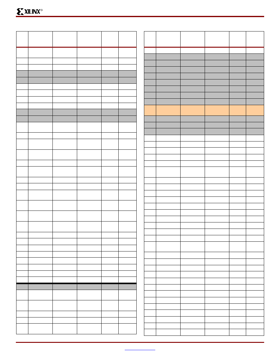
Spartan-3 1.2V FPGA Family: Pinout Descriptions
DS099-4 (v1.2.2) October 9, 2003
www.xilinx.com
57
Advance Product Specification
1-800-255-7778
R
5
IO_L19P_5/
VREF_5
IO_L19P_5/
VREF_5
IO_L19P_5/
VREF_5
Y10
VREF
5
IO_L22N_5
IO_L22N_5
IO_L22N_5
AC10
I/O
5
IO_L22P_5
IO_L22P_5
IO_L22P_5
AB10
I/O
5
N.C. (
)
IO_L23N_5
IO_L23N_5
AF10
I/O
5
N.C. (
)
IO_L23P_5
IO_L23P_5
AE10
I/O
5
IO_L24N_5
IO_L24N_5
IO_L24N_5
Y11
I/O
5
IO_L24P_5
IO_L24P_5
IO_L24P_5
W11
I/O
5
IO_L25N_5
IO_L25N_5
IO_L25N_5
AB11
I/O
5
IO_L25P_5
IO_L25P_5
IO_L25P_5
AA11
I/O
5
N.C. (
)
IO_L26N_5
IO_L26N_5
AF11
I/O
5
N.C. (
)
IO_L26P_5
IO_L26P_5
AE11
I/O
5
IO_L27N_5/
VREF_5
IO_L27N_5/
VREF_5
IO_L27N_5/
VREF_5
Y12
VREF
5
IO_L27P_5
IO_L27P_5
IO_L27P_5
W12
I/O
5
IO_L28N_5/
D6
IO_L28N_5/
D6
IO_L28N_5/
D6
AB12
DUAL
5
IO_L28P_5/
D7
IO_L28P_5/
D7
IO_L28P_5/
D7
AA12
DUAL
5
IO_L29N_5
IO_L29N_5
IO_L29N_5
AF12
I/O
5
IO_L29P_5/
VREF_5
IO_L29P_5/
VREF_5
IO_L29P_5/
VREF_5
AE12
VREF
5
IO_L30N_5
IO_L30N_5
IO_L30N_5
Y13
I/O
5
IO_L30P_5
IO_L30P_5
IO_L30P_5
W13
I/O
5
IO_L31N_5/
D4
IO_L31N_5/
D4
IO_L31N_5/
D4
AC13
DUAL
5
IO_L31P_5/
D5
IO_L31P_5/
D5
IO_L31P_5/
D5
AB13
DUAL
5
IO_L32N_5/
GCLK3
IO_L32N_5/
GCLK3
IO_L32N_5/
GCLK3
AE13
GCLK
5
IO_L32P_5/
GCLK2
IO_L32P_5/
GCLK2
IO_L32P_5/
GCLK2
AD13
GCLK
5
VCCO_5
VCCO_5
VCCO_5
AD7
VCCO
5
VCCO_5
VCCO_5
VCCO_5
AD11
VCCO
5
VCCO_5
VCCO_5
VCCO_5
U13
VCCO
5
VCCO_5
VCCO_5
VCCO_5
V11
VCCO
5
VCCO_5
VCCO_5
VCCO_5
V12
VCCO
5
VCCO_5
VCCO_5
VCCO_5
V13
VCCO
5
VCCO_5
VCCO_5
VCCO_5
W9
VCCO
5
VCCO_5
VCCO_5
VCCO_5
W10
VCCO
6
N.C. (
)
N.C. ( )
IO
AA5
I/O
6
IO_L01N_6/
VRP_6
IO_L01N_6/
VRP_6
IO_L01N_6/
VRP_6
AD2
DCI
6
IO_L01P_6/
VRN_6
IO_L01P_6/
VRN_6
IO_L01P_6/
VRN_6
AD1
DCI
6
IO_L02N_6
IO_L02N_6
IO_L02N_6
AB4
I/O
6
IO_L02P_6
IO_L02P_6
IO_L02P_6
AB3
I/O
6
IO_L03N_6/
VREF_6
IO_L03N_6/
VREF_6
IO_L03N_6/
VREF_6
AC2
VREF
Table 28: FG676 Package Pinout (Continued)
Bank
XC3S1000
Pin Name
XC3S1500
Pin Name
XC3S2000
Pin Name
FG676
Pin
Number
Type
6
IO_L03P_6
IO_L03P_6
IO_L03P_6
AC1
I/O
6
N.C. (
)
IO_L05N_6
IO_L05N_6
AB2
I/O
6
N.C. (
)
IO_L05P_6
IO_L05P_6
AB1
I/O
6
N.C. (
)
IO_L06N_6
IO_L06N_6
Y7
I/O
6
N.C. (
)
IO_L06P_6
IO_L06P_6
Y6
I/O
6
N.C. (
)
IO_L07N_6
IO_L07N_6
AA4
I/O
6
N.C. (
)
IO_L07P_6
IO_L07P_6
AA3
I/O
6
N.C. (
)
IO_L08N_6
IO_L08N_6
Y5
I/O
6
N.C. (
)
IO_L08P_6
IO_L08P_6
Y4
I/O
6
N.C. (
)
IO_L09N_6/
VREF_6
IO_L09N_6/
VREF_6
AA2
VREF
6
N.C. (
)
IO_L09P_6
IO_L09P_6
AA1
I/O
6
N.C. (
)
IO_L10N_6
IO_L10N_6
Y2
I/O
6
N.C. (
)
IO_L10P_6
IO_L10P_6
Y1
I/O
6
IO_L14N_6
IO_L14N_6
IO_L14N_6
W7
I/O
6
IO_L14P_6
IO_L14P_6
IO_L14P_6
W6
I/O
6
IO_L16N_6
IO_L16N_6
IO_L16N_6
V6
I/O
6
IO_L16P_6
IO_L16P_6
IO_L16P_6
W5
I/O
6
IO_L17N_6
IO_L17N_6
IO_L17N_6
W4
I/O
6
IO_L17P_6/
VREF_6
IO_L17P_6/
VREF_6
IO_L17P_6/
VREF_6
W3
VREF
6
IO_L19N_6
IO_L19N_6
IO_L19N_6
W2
I/O
6
IO_L19P_6
IO_L19P_6
IO_L19P_6
W1
I/O
6
IO_L20N_6
IO_L20N_6
IO_L20N_6
V7
I/O
6
IO_L20P_6
IO_L20P_6
IO_L20P_6
U7
I/O
6
IO_L21N_6
IO_L21N_6
IO_L21N_6
V5
I/O
6
IO_L21P_6
IO_L21P_6
IO_L21P_6
V4
I/O
6
IO_L22N_6
IO_L22N_6
IO_L22N_6
V3
I/O
6
IO_L22P_6
IO_L22P_6
IO_L22P_6
V2
I/O
6
IO_L23N_6
IO_L23N_6
IO_L23N_6
U6
I/O
6
IO_L23P_6
IO_L23P_6
IO_L23P_6
U5
I/O
6
IO_L24N_6/
VREF_6
IO_L24N_6/
VREF_6
IO_L24N_6/
VREF_6
U4
VREF
6
IO_L24P_6
IO_L24P_6
IO_L24P_6
U3
I/O
6
IO_L26N_6
IO_L26N_6
IO_L26N_6
U2
I/O
6
IO_L26P_6
IO_L26P_6
IO_L26P_6
U1
I/O
6
IO_L27N_6
IO_L27N_6
IO_L27N_6
T8
I/O
6
IO_L27P_6
IO_L27P_6
IO_L27P_6
T7
I/O
6
IO_L28N_6
IO_L28N_6
IO_L28N_6
T6
I/O
6
IO_L28P_6
IO_L28P_6
IO_L28P_6
T5
I/O
6
IO_L29N_6
IO_L29N_6
IO_L29N_6
T2
I/O
6
IO_L29P_6
IO_L29P_6
IO_L29P_6
T1
I/O
6
IO_L31N_6
IO_L31N_6
IO_L31N_6
R8
I/O
6
IO_L31P_6
IO_L31P_6
IO_L31P_6
R7
I/O
6
IO_L32N_6
IO_L32N_6
IO_L32N_6
R6
I/O
6
IO_L32P_6
IO_L32P_6
IO_L32P_6
R5
I/O
Table 28: FG676 Package Pinout (Continued)
Bank
XC3S1000
Pin Name
XC3S1500
Pin Name
XC3S2000
Pin Name
FG676
Pin
Number
Type
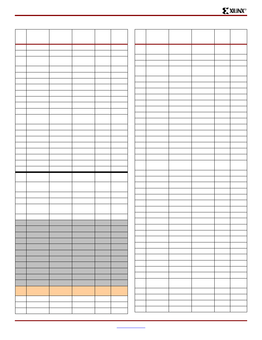
Spartan-3 1.2V FPGA Family: Pinout Descriptions
58
www.xilinx.com
DS099-4 (v1.2.2) October 9, 2003
1-800-255-7778
Advance Product Specification
R
6
IO_L33N_6
IO_L33N_6
IO_L33N_6
T4
I/O
6
IO_L33P_6
IO_L33P_6
IO_L33P_6
R3
I/O
6
IO_L34N_6/
VREF_6
IO_L34N_6/
VREF_6
IO_L34N_6/
VREF_6
R2
VREF
6
IO_L34P_6
IO_L34P_6
IO_L34P_6
R1
I/O
6
IO_L35N_6
IO_L35N_6
IO_L35N_6
P8
I/O
6
IO_L35P_6
IO_L35P_6
IO_L35P_6
P7
I/O
6
IO_L38N_6
IO_L38N_6
IO_L38N_6
P6
I/O
6
IO_L38P_6
IO_L38P_6
IO_L38P_6
P5
I/O
6
IO_L39N_6
IO_L39N_6
IO_L39N_6
P4
I/O
6
IO_L39P_6
IO_L39P_6
IO_L39P_6
P3
I/O
6
IO_L40N_6
IO_L40N_6
IO_L40N_6
P2
I/O
6
IO_L40P_6/
VREF_6
IO_L40P_6/
VREF_6
IO_L40P_6/
VREF_6
P1
VREF
6
VCCO_6
VCCO_6
VCCO_6
P9
VCCO
6
VCCO_6
VCCO_6
VCCO_6
P10
VCCO
6
VCCO_6
VCCO_6
VCCO_6
R9
VCCO
6
VCCO_6
VCCO_6
VCCO_6
T3
VCCO
6
VCCO_6
VCCO_6
VCCO_6
T9
VCCO
6
VCCO_6
VCCO_6
VCCO_6
U8
VCCO
6
VCCO_6
VCCO_6
VCCO_6
V8
VCCO
6
VCCO_6
VCCO_6
VCCO_6
Y3
VCCO
7
IO_L01N_7/
VRP_7
IO_L01N_7/
VRP_7
IO_L01N_7/
VRP_7
F5
DCI
7
IO_L01P_7/
VRN_7
IO_L01P_7/
VRN_7
IO_L01P_7/
VRN_7
F6
DCI
7
IO_L02N_7
IO_L02N_7
IO_L02N_7
E3
I/O
7
IO_L02P_7
IO_L02P_7
IO_L02P_7
E4
I/O
7
IO_L03N_7/
VREF_7
IO_L03N_7/
VREF_7
IO_L03N_7/
VREF_7
D1
VREF
7
IO_L03P_7
IO_L03P_7
IO_L03P_7
D2
I/O
7
N.C. (
)
IO_L05N_7
IO_L05N_7
G6
I/O
7
N.C. (
)
IO_L05P_7
IO_L05P_7
G7
I/O
7
N.C. (
)
IO_L06N_7
IO_L06N_7
E1
I/O
7
N.C. (
)
IO_L06P_7
IO_L06P_7
E2
I/O
7
N.C. (
)
IO_L07N_7
IO_L07N_7
F3
I/O
7
N.C. (
)
IO_L07P_7
IO_L07P_7
F4
I/O
7
N.C. (
)
IO_L08N_7
IO_L08N_7
G4
I/O
7
N.C. (
)
IO_L08P_7
IO_L08P_7
G5
I/O
7
N.C. (
)
IO_L09N_7
IO_L09N_7
F1
I/O
7
N.C. (
)
IO_L09P_7
IO_L09P_7
F2
I/O
7
N.C. (
)
IO_L10N_7
IO_L10N_7
H6
I/O
7
N.C. (
)
IO_L10P_7/
VREF_7
IO_L10P_7/
VREF_7
H7
VREF
7
IO_L14N_7
IO_L14N_7
IO_L14N_7
G1
I/O
7
IO_L14P_7
IO_L14P_7
IO_L14P_7
G2
I/O
7
IO_L16N_7
IO_L16N_7
IO_L16N_7
J6
I/O
Table 28: FG676 Package Pinout (Continued)
Bank
XC3S1000
Pin Name
XC3S1500
Pin Name
XC3S2000
Pin Name
FG676
Pin
Number
Type
7
IO_L16P_7/
VREF_7
IO_L16P_7/
VREF_7
IO_L16P_7/
VREF_7
H5
VREF
7
IO_L17N_7
IO_L17N_7
IO_L17N_7
H3
I/O
7
IO_L17P_7
IO_L17P_7
IO_L17P_7
H4
I/O
7
IO_L19N_7/
VREF_7
IO_L19N_7/
VREF_7
IO_L19N_7/
VREF_7
H1
VREF
7
IO_L19P_7
IO_L19P_7
IO_L19P_7
H2
I/O
7
IO_L20N_7
IO_L20N_7
IO_L20N_7
K7
I/O
7
IO_L20P_7
IO_L20P_7
IO_L20P_7
J7
I/O
7
IO_L21N_7
IO_L21N_7
IO_L21N_7
J4
I/O
7
IO_L21P_7
IO_L21P_7
IO_L21P_7
J5
I/O
7
IO_L22N_7
IO_L22N_7
IO_L22N_7
J2
I/O
7
IO_L22P_7
IO_L22P_7
IO_L22P_7
J3
I/O
7
IO_L23N_7
IO_L23N_7
IO_L23N_7
K5
I/O
7
IO_L23P_7
IO_L23P_7
IO_L23P_7
K6
I/O
7
IO_L24N_7
IO_L24N_7
IO_L24N_7
K3
I/O
7
IO_L24P_7
IO_L24P_7
IO_L24P_7
K4
I/O
7
IO_L26N_7
IO_L26N_7
IO_L26N_7
K1
I/O
7
IO_L26P_7
IO_L26P_7
IO_L26P_7
K2
I/O
7
IO_L27N_7
IO_L27N_7
IO_L27N_7
L7
I/O
7
IO_L27P_7/
VREF_7
IO_L27P_7/
VREF_7
IO_L27P_7/
VREF_7
L8
VREF
7
IO_L28N_7
IO_L28N_7
IO_L28N_7
L5
I/O
7
IO_L28P_7
IO_L28P_7
IO_L28P_7
L6
I/O
7
IO_L29N_7
IO_L29N_7
IO_L29N_7
L1
I/O
7
IO_L29P_7
IO_L29P_7
IO_L29P_7
L2
I/O
7
IO_L31N_7
IO_L31N_7
IO_L31N_7
M7
I/O
7
IO_L31P_7
IO_L31P_7
IO_L31P_7
M8
I/O
7
IO_L32N_7
IO_L32N_7
IO_L32N_7
M6
I/O
7
IO_L32P_7
IO_L32P_7
IO_L32P_7
M5
I/O
7
IO_L33N_7
IO_L33N_7
IO_L33N_7
M3
I/O
7
IO_L33P_7
IO_L33P_7
IO_L33P_7
L4
I/O
7
IO_L34N_7
IO_L34N_7
IO_L34N_7
M1
I/O
7
IO_L34P_7
IO_L34P_7
IO_L34P_7
M2
I/O
7
IO_L35N_7
IO_L35N_7
IO_L35N_7
N7
I/O
7
IO_L35P_7
IO_L35P_7
IO_L35P_7
N8
I/O
7
IO_L38N_7
IO_L38N_7
IO_L38N_7
N5
I/O
7
IO_L38P_7
IO_L38P_7
IO_L38P_7
N6
I/O
7
IO_L39N_7
IO_L39N_7
IO_L39N_7
N3
I/O
7
IO_L39P_7
IO_L39P_7
IO_L39P_7
N4
I/O
7
IO_L40N_7/
VREF_7
IO_L40N_7/
VREF_7
IO_L40N_7/
VREF_7
N1
VREF
7
IO_L40P_7
IO_L40P_7
IO_L40P_7
N2
I/O
7
VCCO_7
VCCO_7
VCCO_7
G3
VCCO
7
VCCO_7
VCCO_7
VCCO_7
J8
VCCO
7
VCCO_7
VCCO_7
VCCO_7
K8
VCCO
Table 28: FG676 Package Pinout (Continued)
Bank
XC3S1000
Pin Name
XC3S1500
Pin Name
XC3S2000
Pin Name
FG676
Pin
Number
Type
Spartan-3 1.2V FPGA Family: Pinout Descriptions
DS099-4 (v1.2.2) October 9, 2003
www.xilinx.com
59
Advance Product Specification
1-800-255-7778
R
7
VCCO_7
VCCO_7
VCCO_7
L3
VCCO
7
VCCO_7
VCCO_7
VCCO_7
L9
VCCO
7
VCCO_7
VCCO_7
VCCO_7
M9
VCCO
7
VCCO_7
VCCO_7
VCCO_7
N9
VCCO
7
VCCO_7
VCCO_7
VCCO_7
N10
VCCO
N/A
GND
GND
GND
A1
GND
N/A
GND
GND
GND
A26
GND
N/A
GND
GND
GND
AC4
GND
N/A
GND
GND
GND
AC12
GND
N/A
GND
GND
GND
AC15
GND
N/A
GND
GND
GND
AC23
GND
N/A
GND
GND
GND
AD3
GND
N/A
GND
GND
GND
AD24
GND
N/A
GND
GND
GND
AE2
GND
N/A
GND
GND
GND
AE25
GND
N/A
GND
GND
GND
AF1
GND
N/A
GND
GND
GND
AF26
GND
N/A
GND
GND
GND
B2
GND
N/A
GND
GND
GND
B25
GND
N/A
GND
GND
GND
C3
GND
N/A
GND
GND
GND
C24
GND
N/A
GND
GND
GND
D4
GND
N/A
GND
GND
GND
D12
GND
N/A
GND
GND
GND
D15
GND
N/A
GND
GND
GND
D23
GND
N/A
GND
GND
GND
K11
GND
N/A
GND
GND
GND
K12
GND
N/A
GND
GND
GND
K15
GND
N/A
GND
GND
GND
K16
GND
N/A
GND
GND
GND
L10
GND
N/A
GND
GND
GND
L11
GND
N/A
GND
GND
GND
L12
GND
N/A
GND
GND
GND
L13
GND
N/A
GND
GND
GND
L14
GND
N/A
GND
GND
GND
L15
GND
N/A
GND
GND
GND
L16
GND
N/A
GND
GND
GND
L17
GND
N/A
GND
GND
GND
M4
GND
N/A
GND
GND
GND
M10
GND
N/A
GND
GND
GND
M11
GND
N/A
GND
GND
GND
M12
GND
N/A
GND
GND
GND
M13
GND
N/A
GND
GND
GND
M14
GND
N/A
GND
GND
GND
M15
GND
N/A
GND
GND
GND
M16
GND
Table 28: FG676 Package Pinout (Continued)
Bank
XC3S1000
Pin Name
XC3S1500
Pin Name
XC3S2000
Pin Name
FG676
Pin
Number
Type
N/A
GND
GND
GND
M17
GND
N/A
GND
GND
GND
M23
GND
N/A
GND
GND
GND
N11
GND
N/A
GND
GND
GND
N12
GND
N/A
GND
GND
GND
N13
GND
N/A
GND
GND
GND
N14
GND
N/A
GND
GND
GND
N15
GND
N/A
GND
GND
GND
N16
GND
N/A
GND
GND
GND
P11
GND
N/A
GND
GND
GND
P12
GND
N/A
GND
GND
GND
P13
GND
N/A
GND
GND
GND
P14
GND
N/A
GND
GND
GND
P15
GND
N/A
GND
GND
GND
P16
GND
N/A
GND
GND
GND
R4
GND
N/A
GND
GND
GND
R10
GND
N/A
GND
GND
GND
R11
GND
N/A
GND
GND
GND
R12
GND
N/A
GND
GND
GND
R13
GND
N/A
GND
GND
GND
R14
GND
N/A
GND
GND
GND
R15
GND
N/A
GND
GND
GND
R16
GND
N/A
GND
GND
GND
R17
GND
N/A
GND
GND
GND
R23
GND
N/A
GND
GND
GND
T10
GND
N/A
GND
GND
GND
T11
GND
N/A
GND
GND
GND
T12
GND
N/A
GND
GND
GND
T13
GND
N/A
GND
GND
GND
T14
GND
N/A
GND
GND
GND
T15
GND
N/A
GND
GND
GND
T16
GND
N/A
GND
GND
GND
T17
GND
N/A
GND
GND
GND
U11
GND
N/A
GND
GND
GND
U12
GND
N/A
GND
GND
GND
U15
GND
N/A
GND
GND
GND
U16
GND
N/A
VCCAUX
VCCAUX
VCCAUX
A2
VCCAUX
N/A
VCCAUX
VCCAUX
VCCAUX
A9
VCCAUX
N/A
VCCAUX
VCCAUX
VCCAUX
A18
VCCAUX
N/A
VCCAUX
VCCAUX
VCCAUX
A25
VCCAUX
N/A
VCCAUX
VCCAUX
VCCAUX
AE1
VCCAUX
N/A
VCCAUX
VCCAUX
VCCAUX
AE26
VCCAUX
N/A
VCCAUX
VCCAUX
VCCAUX
AF2
VCCAUX
N/A
VCCAUX
VCCAUX
VCCAUX
AF9
VCCAUX
N/A
VCCAUX
VCCAUX
VCCAUX
AF18
VCCAUX
Table 28: FG676 Package Pinout (Continued)
Bank
XC3S1000
Pin Name
XC3S1500
Pin Name
XC3S2000
Pin Name
FG676
Pin
Number
Type
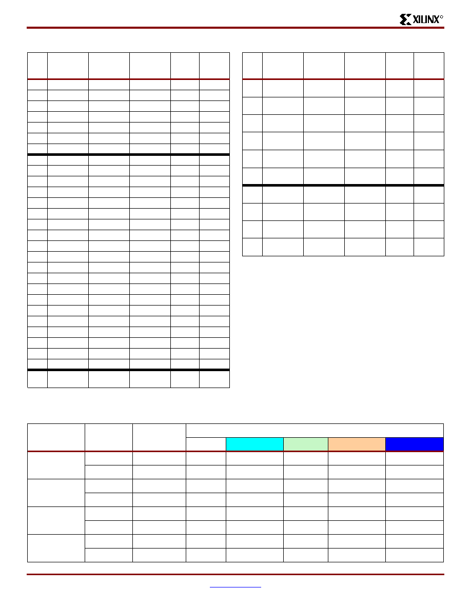
Spartan-3 1.2V FPGA Family: Pinout Descriptions
60
www.xilinx.com
DS099-4 (v1.2.2) October 9, 2003
1-800-255-7778
Advance Product Specification
R
User I/Os by Bank
Table 29
indicates how the available user-I/O pins are dis-
tributed between the eight I/O banks for the XC3S1000 in
the FG676 package. Similarly,
Table 30
shows how the
available user-I/O pins are distributed between the eight I/O
banks for the XC3S1500 in the FG676 package. Finally,
Table 31
shows the same information for the XC3S2000 in
the FG676 package.
N/A
VCCAUX
VCCAUX
VCCAUX
AF25
VCCAUX
N/A
VCCAUX
VCCAUX
VCCAUX
B1
VCCAUX
N/A
VCCAUX
VCCAUX
VCCAUX
B26
VCCAUX
N/A
VCCAUX
VCCAUX
VCCAUX
J1
VCCAUX
N/A
VCCAUX
VCCAUX
VCCAUX
J26
VCCAUX
N/A
VCCAUX
VCCAUX
VCCAUX
V1
VCCAUX
N/A
VCCAUX
VCCAUX
VCCAUX
V26
VCCAUX
N/A
VCCINT
VCCINT
VCCINT
H8
VCCINT
N/A
VCCINT
VCCINT
VCCINT
H19
VCCINT
N/A
VCCINT
VCCINT
VCCINT
J9
VCCINT
N/A
VCCINT
VCCINT
VCCINT
J10
VCCINT
N/A
VCCINT
VCCINT
VCCINT
J17
VCCINT
N/A
VCCINT
VCCINT
VCCINT
J18
VCCINT
N/A
VCCINT
VCCINT
VCCINT
K9
VCCINT
N/A
VCCINT
VCCINT
VCCINT
K10
VCCINT
N/A
VCCINT
VCCINT
VCCINT
K17
VCCINT
N/A
VCCINT
VCCINT
VCCINT
K18
VCCINT
N/A
VCCINT
VCCINT
VCCINT
U9
VCCINT
N/A
VCCINT
VCCINT
VCCINT
U10
VCCINT
N/A
VCCINT
VCCINT
VCCINT
U17
VCCINT
N/A
VCCINT
VCCINT
VCCINT
U18
VCCINT
N/A
VCCINT
VCCINT
VCCINT
V9
VCCINT
N/A
VCCINT
VCCINT
VCCINT
V10
VCCINT
N/A
VCCINT
VCCINT
VCCINT
V17
VCCINT
N/A
VCCINT
VCCINT
VCCINT
V18
VCCINT
N/A
VCCINT
VCCINT
VCCINT
W8
VCCINT
N/A
VCCINT
VCCINT
VCCINT
W19
VCCINT
VCC
AUX
CCLK
CCLK
CCLK
AD26
CONFIG
Table 28: FG676 Package Pinout (Continued)
Bank
XC3S1000
Pin Name
XC3S1500
Pin Name
XC3S2000
Pin Name
FG676
Pin
Number
Type
VCC
AUX
DONE
DONE
DONE
AC24
CONFIG
VCC
AUX
HSWAP_EN
HSWAP_EN
HSWAP_EN
C2
CONFIG
VCC
AUX
M0
M0
M0
AE3
CONFIG
VCC
AUX
M1
M1
M1
AC3
CONFIG
VCC
AUX
M2
M2
M2
AF3
CONFIG
VCC
AUX
PROG_B
PROG_B
PROG_B
D3
CONFIG
VCC
AUX
TCK
TCK
TCK
B24
JTAG
VCC
AUX
TDI
TDI
TDI
C1
JTAG
VCC
AUX
TDO
TDO
TDO
D24
JTAG
VCC
AUX
TMS
TMS
TMS
A24
JTAG
Table 28: FG676 Package Pinout (Continued)
Bank
XC3S1000
Pin Name
XC3S1500
Pin Name
XC3S2000
Pin Name
FG676
Pin
Number
Type
Table 29: User I/Os Per Bank for XC3S1000 in FG676 Package
Edge
I/O
Bank
Maximum
I/O
All Possible I/O Pins by Type
I/O
DUAL
DCI
VREF
GCLK
Top
0
49
40
0
2
5
2
1
50
41
0
2
5
2
Right
2
48
41
0
2
5
0
3
48
41
0
2
5
0
Bottom
4
50
35
6
2
5
2
5
50
35
6
2
5
2
Left
6
48
41
0
2
5
0
7
48
41
0
2
5
0
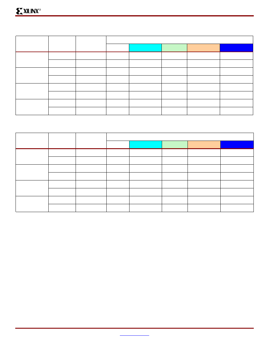
Spartan-3 1.2V FPGA Family: Pinout Descriptions
DS099-4 (v1.2.2) October 9, 2003
www.xilinx.com
61
Advance Product Specification
1-800-255-7778
R
Table 30: User I/Os Per Bank for XC3S1500 in FG676 Package
Edge
I/O
Bank
Maximum
I/O
All Possible I/O Pins by Type
I/O
DUAL
DCI
VREF
GCLK
Top
0
62
52
0
2
6
2
1
61
51
0
2
6
2
Right
2
60
52
0
2
6
0
3
60
52
0
2
6
0
Bottom
4
63
47
6
2
6
2
5
61
45
6
2
6
2
Left
6
60
52
0
2
6
0
7
60
52
0
2
6
0
Table 31: User I/Os Per Bank for XC3S2000 in FG676 Package
Edge
I/O Bank
Maximum
I/O
All Possible I/O Pins by Type
I/O
DUAL
DCI
VREF
GCLK
Top
0
62
52
0
2
6
2
1
61
51
0
2
6
2
Right
2
61
53
0
2
6
0
3
60
52
0
2
6
0
Bottom
4
63
47
6
2
6
2
5
61
45
6
2
6
2
Left
6
61
53
0
2
6
0
7
60
52
0
2
6
0
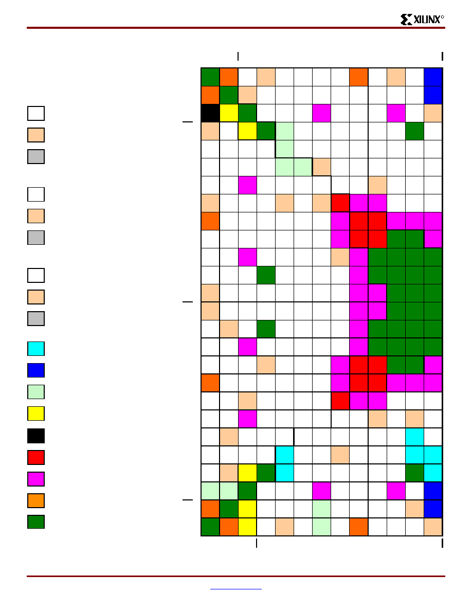
Spartan-3 1.2V FPGA Family: Pinout Descriptions
62
www.xilinx.com
DS099-4 (v1.2.2) October 9, 2003
1-800-255-7778
Advance Product Specification
R
FG676 Footprint
Left Half of Package
(top view)
XC3S1000
(391 max. user I/O)
315
I/O: Unrestricted,
general-purpose user I/O
40
VREF: User I/O or input
voltage reference for bank
98
N.C.: Unconnected pins for
XC3S1000 (
)
XC3S1500
(487 max user I/O)
403
I/O: Unrestricted,
general-purpose user I/O
48
VREF: User I/O or input
voltage reference for bank
2
N.C.: Unconnected pins for
XC3S1500 ( )
XC3S2000
(489 max user I/O)
405
I/O: Unrestricted,
general-purpose user I/O
48
VREF: User I/O or input
voltage reference for bank
0
N.C.: No unconnected pins
All devices
12
DUAL: Configuration pin,
then possible user I/O
8
GCLK: User I/O or global
clock buffer input
16
DCI: User I/O or reference
resistor input for bank
7
CONFIG: Dedicated
configuration pins
4
JTAG: Dedicated JTAG
port pins
20
VCCINT: Internal core
voltage supply (+1.2V)
64
VCCO: Output voltage
supply for bank
16
VCCAUX: Auxiliary voltage
supply (+2.5V)
76
GND: Ground
Figure 13: FG676 Package Footprint (top view)
2
1
10
3
4
5
6
7
8
9
11
12
13
Bank 0
A
B
C
D
E
F
G
H
J
K
L
M
N
P
R
T
U
V
W
Y
A
A
A
B
A
C
A
D
A
E
A
F
Bank 6
Bank 7
Bank 5
VCCAUX
I/O
I/O
L05P_0
VREF_0
I/O
I/O
I/O
L10P_0
I/O
L15P_0
VCCAUX
I/O
L23P_0
I/O
L26P_0
VREF_0
I/O
L29P_0
I/O
L32P_0
GCLK6
VCCAUX
I/O
VREF_0
I/O
L05N_0
I/O
L06P_0
I/O
L08P_0
I/O
L10N_0
I/O
L15N_0
I/O
L18P_0
I/O
L23N_0
I/O
L26N_0
I/O
L29N_0
I/O
L32N_0
GCLK7
TD I
HSWAP_
EN
I/O
I/O
L06N_0
I/O
L08N_0
VCCO_0
I/O
I/O
L18N_0
I/O
L22P_0
VCCO_0
I/O
I/O
L31P_0
VREF_0
I/O
L03N_7
VREF_7
I/O
L03P_7
PROG_B
I/O
L01P_0
VRN_0
I/O
L07P_0
I/O
L09P_0
I/O
L12P_0
I/O
L17P_0
I/O
L22N_0
I/O
L25P_0
GND
GND
GND
GND
GND
GND
GND
GND
GND
GND
GND
GND
GND
GND
GND
GND
GND
GND
GND
GND
GND
GND
GND
GND
GND
GND
GND
I/O
L31N_0
I/O
L06N_7
I/O
L06P_7
I/O
L02N_7
I/O
L02P_7
I/O
L01N_0
VRP_0
I/O
L07N_0
I/O
L09N_0
I/O
L12N_0
I/O
L17N_0
I/O
L19P_0
I/O
L25N_0
I/O
L28P_0
I/O
I/O
L09N_7
I/O
L09P_7
I/O
L07N_7
I/O
L07P_7
I/O
L01N_7
VRP_7
I/O
L01P_7
VRN_7
I/O
VREF_0
I/O
L11P_0
I/O
L16P_0
I/O
L19N_0
I/O
L24P_0
I/O
L28N_0
I/O
L30P_0
I/O
L14N_7
I/O
L14P_7
VCCO_7
I/O
L08N_7
I/O
L08P_7
I/O
L05N_7
I/O
L05P_7
I/O
L11N_0
I/O
L16N_0
I/O
VREF_0
I/O
L24N_0
I/O
L27N_0
I/O
L30N_0
I/O
L19N_7
VREF_7
I/O
L19P_7
I/O
L17N_7
I/O
L17P_7
I/O
L16P_7
VREF_7
I/O
L10N_7
I/O
L10P_7
VREF_7
VCCINT
VCCO_0
VCCO_0
I/O
I/O
I/O
L27P_0
VCCAUX
I/O
L22N_7
I/O
L22P_7
I/O
L21N_7
I/O
L21P_7
I/O
L16N_7
I/O
L20P_7
VCCO_7
VCCINT
VCCINT
VCCO_0
VCCO_0
VCCO_0
I/O
L26N_7
I/O
L26P_7
I/O
L24N_7
I/O
L24P_7
I/O
L23N_7
I/O
L23P_7
I/O
L20N_7
VCCO_7
VCCINT
VCCINT
VCCO_0
I/O
L29N_7
I/O
L29P_7
VCCO_7
I/O
L33P_7
I/O
L28N_7
I/O
L28P_7
I/O
L27N_7
I/O
L27P_7
VREF_7
VCCO_7
I/O
L34N_7
I/O
L34P_7
I/O
L33N_7
I/O
L32P_7
I/O
L32N_7
I/O
L31N_7
I/O
L31P_7
VCCO_7
I/O
L40N_7
VREF_7
I/O
L40P_7
I/O
L39N_7
I/O
L39P_7
I/O
L38N_7
I/O
L38P_7
I/O
L35N_7
I/O
L35P_7
VCCO_7
VCCO_7
I/O
L40P_6
VREF_6
I/O
L40N_6
I/O
L39P_6
I/O
L39N_6
I/O
L38P_6
I/O
L38N_6
I/O
L35P_6
I/O
L35N_6
VCCO_6
VCCO_6
I/O
L34P_6
I/O
L34N_6
VREF_6
I/O
L33P_6
GND
GND
GND
GND
GND
GND
I/O
L32P_6
I/O
L32N_6
I/O
L31P_6
I/O
L31N_6
VCCO_6
I/O
L29P_6
I/O
L29N_6
VCCO_6
I/O
L33N_6
I/O
L28P_6
I/O
L28N_6
I/O
L27P_6
I/O
L27N_6
VCCO_6
I/O
L26P_6
I/O
L26N_6
I/O
L24P_6
I/O
L24N_6
VREF_6
I/O
L23P_6
I/O
L23N_6
I/O
L20P_6
VCCO_6
VCCINT
VCCINT
VCCO_5
VCCAUX
I/O
L22P_6
I/O
L22N_6
I/O
L21P_6
I/O
L21N_6
I/O
L16N_6
I/O
L20N_6
VCCO_6
VCCINT
VCCINT
VCCO_5
VCCO_5
VCCO_5
I/O
L19P_6
I/O
L19N_6
I/O
L17P_6
VREF_6
I/O
L17N_6
I/O
L16P_6
I/O
L14P_6
I/O
L14N_6
VCCINT
VCCO_5
VCCO_5
I/O
L24P_5
I/O
L27P_5
I/O
L30P_5
I/O
L10P_6
I/O
L10N_6 VCCO_6
I/O
L08P_6
I/O
L08N_6
I/O
L06P_6
I/O
L06N_6
I/O
I/O
L16P_5
I/O
L19P_5
VREF_5
I/O
L24N_5
I/O
L27N_5
VREF_5
I/O
L30N_5
I/O
L09P_6
I/O
L09N_6
VREF_6
I/O
L07P_6
I/O
L07N_6
I/O
I/O
L05P_5
I/O
I/O
L11P_5
I/O
L16N_5
I/O
L19N_5
I/O
L25P_5
I/O
L28P_5
D7
I/O
I/O
L05P_6
I/O
L05N_6
I/O
L02P_6
I/O
L02N_6
I/O
L01P_5
CS_B
I/O
L05N_5
I/O
L09P_5
I/O
L11N_5
VREF_5
I/O
I/O
L22P_5
I/O
L25N_5
I/O
L28N_5
D6
I/O
L31P_5
D5
I/O
L03P_6
I/O
L03N_6
VREF_6
M1
I/O
L01N_5
RDWR_B
I/O
L07P_5
I/O
L09N_5
I/O
L12P_5
I/O
I/O
L22N_5
I/O
GND
GND
GND
GND
GND
I/O
L31N_5
D4
I/O
L01P_6
VRN_6
I/O
L01N_6
VRP_6
I/O
L04P_5
I/O
L06P_5
I/O
L07N_5
VCCO_5
I/O
L12N_5
I/O
L18P_5
I/O
VCCO_5
I/O
I/O
L32P_5
GCLK2
VCCAUX
M0
I/O
L04N_5
I/O
L06N_5
I/O
L08P_5
I/O
L10P_5
VRN_5
I/O
L15P_5
I/O
L18N_5
I/O
L23P_5
I/O
L26P_5
I/O
L29P_5
VREF_5
I/O
L32N_5
GCLK3
VCCAUX
M2
I/O
I/O
VREF_5
I/O
L08N_5
I/O
L10N_5
VRP_5
I/O
L15N_5
VCCAUX
I/O
L23N_5
I/O
L26N_5
I/O
L29N_5
I/O
VREF_5
DS099-4_12a_030203
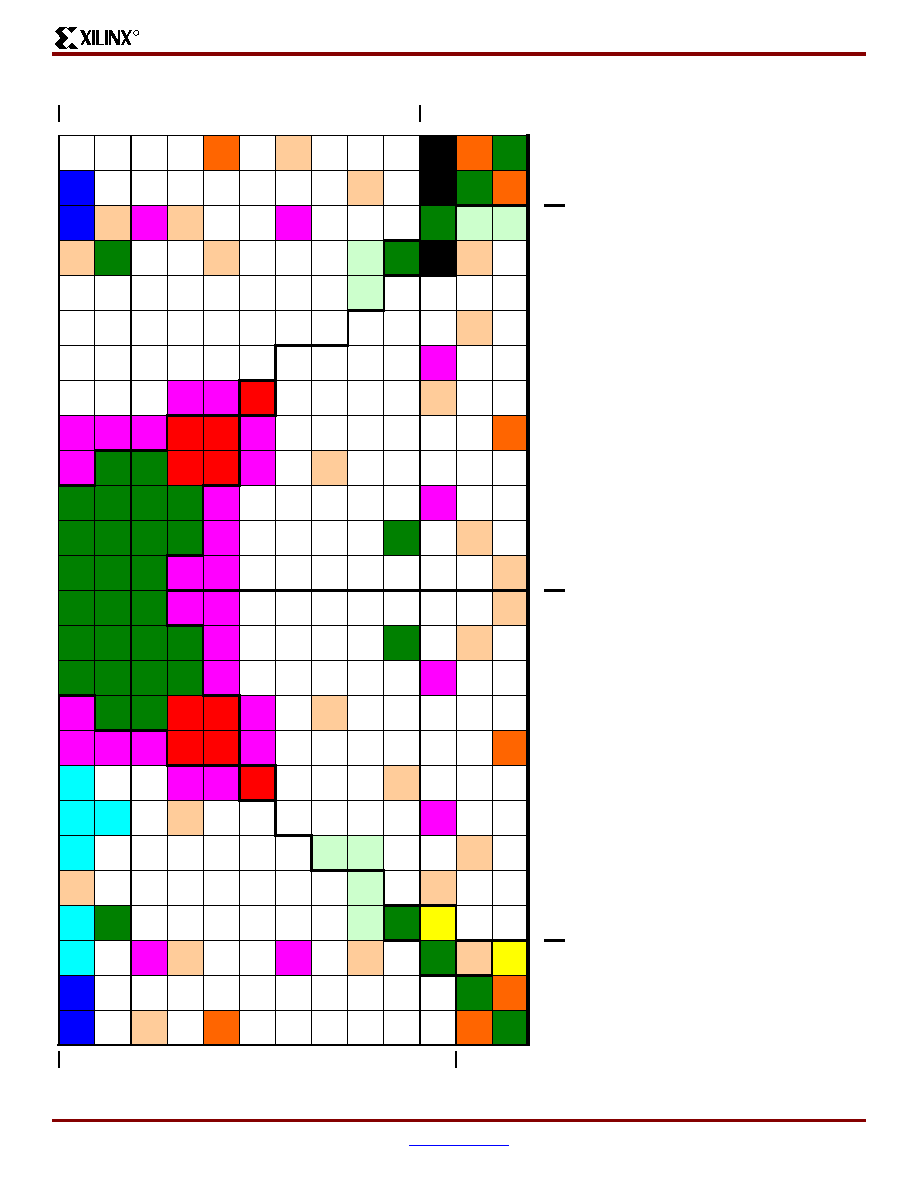
Spartan-3 1.2V FPGA Family: Pinout Descriptions
DS099-4 (v1.2.2) October 9, 2003
www.xilinx.com
63
Advance Product Specification
1-800-255-7778
R
Right Half of Package
(top view)
2
14
15
16
17
18
19
20
21
22
23
24
25
26
Bank 1
Bank 4
A
B
C
D
E
F
G
H
J
K
L
M
N
P
R
T
U
V
W
Y
A
A
A
B
A
C
A
D
A
E
A
F
Bank 2
Bank 3
I/O
I/O
L29N_1
I/O
L26N_1
I/O
L23N_1 VCCAUX
I/O
L15N_1
I/O
L10N_1
VREF_1
I/O
L08N_1
I/O
I/O
TMS
VCCAUX
I/O
L32N_1
GCLK5
I/O
L29P_1
I/O
L26P_1
I/O
L23P_1
I/O
L18N_1
I/O
L15P_1
I/O
L10P_1
I/O
L08P_1
I/O
L06N_1
VREF_1
I/O
L04N_1
TCK
VCCAUX
I/O
L32P_1
GCLK4
I/O
VREF_1
VCCO_1
I/O
VREF_1
I/O
L18P_1
I/O
L12N_1 VCCO_1
I/O
L07N_1
I/O
L06P_1
I/O
L04P_1
I/O
L01N_2
VRP_2
I/O
L01P_2
VRN_
I/O
L31N_1
VREF_1
GND
I/O
I/O
L22N_1
I/O
VREF_1
I/O
L12P_1
I/O
L09N_1
I/O
L07P_1
I/O
L01N_1
VRP_1
GND
GND
GND
GND
GND
GND
GND
GND
GND
GND
GND
GND
GND
GND
GND
GND
GND
GND
GND
GND
GND
GND
GND
GND
GND
GND
GND
GND
GND
GND
GND
GND
GND
GND
GND
GND
GND
TDO
I/O
L03N_2
VREF_2
I/O
L03P_2
I/O
L31P_1
I/O
L28N_1
I/O
L25N_1
I/O
L22P_1
I/O
I/O
L11N_1
I/O
L09P_1
I/O
L05N_1
I/O
L01P_1
VRN_1
I/O
L02N_2
I/O
L02P_2
I/O
L05N_2
I/O
L05P_2
I/O
I/O
L28P_1
I/O
L25P_1
I/O
L19N_1
I/O
L16N_1
I/O
L11P_1
I/O
I/O
L05P_1
I/O
I/O
L07N_2
I/O
L07P_2
I/O
L09N_2
VREF_2
I/O
L09P_2
I/O
L30N_1
I/O
L27N_1
I/O
L24N_1
I/O
L19P_1
I/O
L16P_1
I/O
I/O
L06N_2
I/O
L06P_2
I/O
L08N_2
I/O
L08P_2 VCCO_2
I/O
L10N_2
I/O
L10P_2
I/O
L30P_1
I/O
L27P_1
I/O
L24P_1
VCCO_1
VCCO_1
VCCINT
I/O
L14N_2
I/O
L14P_2
I/O
L16N_2
I/O
L17N_2
I/O
L17P_2
VREF_2
I/O
L19N_2
I/O
L19P_2
VCCO_1
VCCO_1
VCCO_1
VCCINT
VCCINT
VCCO_2
I/O
L20N_2
I/O
L16P_2
I/O
L21N_2
I/O
L21P_2
I/O
L22N_2
I/O
L22P_2
VCCAUX
VCCO_1
VCCINT
VCCINT
VCCO_2
I/O
L20P_2
I/O
L23N_2
VREF_2
I/O
L23P_2
I/O
L24N_2
I/O
L24P_2
I/O
L26N_2
I/O
L26P_2
VCCO_2
I/O
L27N_2
I/O
L27P_2
I/O
L28N_2
I/O
L28P_2
I/O
L33N_2
VCCO_2
I/O
L29N_2
I/O
L29P_2
VCCO_2
I/O
L31N_2
I/O
L31P_2
I/O
L32N_2
I/O
L32P_2
I/O
L33P_2
I/O
L34N_2
VREF_2
I/O
L34P_2
VCCO_2
VCCO_2
I/O
L35N_2
I/O
L35P_2
I/O
L38N_2
I/O
L38P_2
I/O
L39N_2
I/O
L39P_2
I/O
L40N_2
I/O
L40P_2
VREF_2
VCCO_3
VCCO_3
I/O
L35P_3
I/O
L35N_3
I/O
L38P_3
I/O
L38N_3
I/O
L39P_3
I/O
L39N_3
I/O
L40P_3
I/O
L40N_3
VREF_3
VCCO_3
I/O
L31P_3
I/O
L31N_3
I/O
L32P_3
I/O
L32N_3
I/O
L33N_3
I/O
L34P_3
VREF_3
I/O
L34N_3
VCCO_3
I/O
L27P_3
I/O
L27N_3
I/O
L28P_3
I/O
L28N_3
I/O
L33P_3
VCCO_3
I/O
L29P_3
I/O
L29N_3
VCCO_4
VCCINT
VCCINT
VCCO_3
I/O
L20N_3
I/O
L23P_3
VREF_3
I/O
L23N_3
I/O
L24P_3
I/O
L24N_3
I/O
L26P_3
I/O
L26N_3
VCCO_4
VCCO_4
VCCO_4
VCCINT
VCCINT
VCCO_3
I/O
L20P_3
I/O
L16N_3
I/O
L21P_3
I/O
L21N_3
I/O
L22P_3
I/O
L22N_3
VCCAUX
I/O
L27P_4
D1
I/O
I/O
VCCO_4
VCCO_4
VCCINT
I/O
L10P_3
I/O
L10N_3
I/O
L16P_3
I/O
L17P_3
VREF_3
I/O
L17N_3
I/O
L19P_3
I/O
L19N_3
I/O
L30N_4
D2
I/O
L27N_4
DIN
D0
I/O
L24N_4
I/O
VREF_4
I/O
L16N_4
I/O
L11N_4
I/O
L05P_3
I/O
L05N_3
I/O
L08P_3
I/O
L08N_3 VCCO_3
I/O
L14P_3
I/O
L14N_3
I/O
L30P_4
D3
I/O
L28N_4
I/O
L24P_4
I/O
L19P_4
I/O
L16P_4
I/O
L11P_4
I/O
I/O
L01P_3
VRN_3
I/O
L01N_3
VRP_3
I/O
L07P_3
I/O
L07N_3
I/O
L09P_3
VREF_3
I/O
L09N_3
IO
VREF_4
I/O
L28P_4
I/O
L25N_4
I/O
L22P_4
I/O
L17N_4
I/O
L12N_4
I/O
L09N_4
I/O
L07N_4
I/O
L01N_4
VRP_4
I/O
L02P_3
I/O
L02N_3
VREF_3
I/O
L06P_3
I/O
L06N_3
I/O
L31N_4
INIT_B
I/O
L25P_4
I/O
L19N_4
I/O
L17P_4
I/O
L12P_4
I/O
L09P_4
I/O
L07P_4
I/O
L01P_4
VRN_4
DONE
I/O
L03P_3
I/O
L03N_3
I/O
L31P_4
DOUT
BUSY
I/O
VCCO_4
I/O
L22N_4
VREF_4
I/O
L18N_4
I/O
VCCO_4
I/O
L08N_4
I/O
L06N_4
VREF_4
I/O
I/O
VREF_4
CCLK
I/O
L32N_4
GCLK1
I/O
L29N_4
I/O
L26N_4
I/O
L23N_4
I/O
L18P_4
I/O
L15N_4
I/O
L10N_4
I/O
L08P_4
I/O
L06P_4
I/O
L05N_4
I/O
L04N_4
VCCAUX
I/O
L32P_4
GCLK0
I/O
L29P_4
I/O
L26P_4
VREF_4
I/O
L23P_4 VCCAUX
I/O
L15P_4
I/O
L10P_4
I/O
I/O
I/O
L05P_4
I/O
L04P_4
VCCAUX
DS099-4_12b_030203
Spartan-3 1.2V FPGA Family: Pinout Descriptions
64
www.xilinx.com
DS099-4 (v1.2.2) October 9, 2003
1-800-255-7778
Advance Product Specification
R
FG900: 900-lead Fine-pitch Ball Grid
Array
The 900-lead fine-pitch ball grid array package, FG900,
supports three different Spartan-3 devices, including the
XC3S2000, the XC3S4000, and the XC3S5000. The foot-
prints for the XC3S4000 and XC3S5000 are identical, as
shown in
Table 32
and
Figure 14
. The XC3S2000, however,
has fewer I/O pins which consequently results in 68 uncon-
nected pins on the FG900 package, labeled as "N.C." In
Table 32
and
Figure 14
, these unconnected pins are indi-
cated with a black diamond symbol (
).
All the package pins appear in
Table 32
and are sorted by
bank number, then by pin name. Pairs of pins that form a dif-
ferential I/O pair appear together in the table. The table also
shows the pin number for each pin and the pin type, as
defined earlier.
If there is a difference between the XC3S2000 pinout and
the pinout for the XC3S4000 and XC3S5000, then that dif-
ference is highlighted in
Table 32
. If the table entry is
shaded, then there is an unconnected pin on the XC3S2000
that maps to a user-I/O pin on the XC3S4000 and
XC3S5000.
Pinout Table
Table 32: FG900 Package Pinout
Bank
XC3S2000
Pin Name
XC3S4000
XC3S5000
Pin Name
FG900
Pin
Number
Type
0
IO
IO
E15
I/O
0
IO
IO
K15
I/O
0
IO
IO
D13
I/O
0
IO
IO
K13
I/O
0
IO
IO
G8
I/O
0
IO/VREF_0
IO/VREF_0
F9
VREF
0
IO/VREF_0
IO/VREF_0
C4
VREF
0
IO_L01N_0/
VRP_0
IO_L01N_0/
VRP_0
B4
DCI
0
IO_L01P_0/
VRN_0
IO_L01P_0/
VRN_0
A4
DCI
0
IO_L02N_0
IO_L02N_0
B5
I/O
0
IO_L02P_0
IO_L02P_0
A5
I/O
0
IO_L03N_0
IO_L03N_0
D5
I/O
0
IO_L03P_0
IO_L03P_0
E6
I/O
0
IO_L04N_0
IO_L04N_0
C6
I/O
0
IO_L04P_0
IO_L04P_0
B6
I/O
0
IO_L05N_0
IO_L05N_0
F6
I/O
0
IO_L05P_0/
VREF_0
IO_L05P_0/
VREF_0
F7
VREF
0
IO_L06N_0
IO_L06N_0
D7
I/O
0
IO_L06P_0
IO_L06P_0
C7
I/O
0
IO_L07N_0
IO_L07N_0
F8
I/O
0
IO_L07P_0
IO_L07P_0
E8
I/O
0
IO_L08N_0
IO_L08N_0
D8
I/O
0
IO_L08P_0
IO_L08P_0
C8
I/O
0
IO_L09N_0
IO_L09N_0
B8
I/O
0
IO_L09P_0
IO_L09P_0
A8
I/O
0
IO_L10N_0
IO_L10N_0
J9
I/O
0
IO_L10P_0
IO_L10P_0
H9
I/O
0
IO_L11N_0
IO_L11N_0
G10
I/O
0
IO_L11P_0
IO_L11P_0
F10
I/O
0
IO_L12N_0
IO_L12N_0
C10
I/O
0
IO_L12P_0
IO_L12P_0
B10
I/O
0
IO_L13N_0
IO_L13N_0
J10
I/O
0
IO_L13P_0
IO_L13P_0
K11
I/O
0
IO_L14N_0
IO_L14N_0
H11
I/O
0
IO_L14P_0
IO_L14P_0
G11
I/O
0
IO_L15N_0
IO_L15N_0
F11
I/O
0
IO_L15P_0
IO_L15P_0
E11
I/O
0
IO_L16N_0
IO_L16N_0
D11
I/O
0
IO_L16P_0
IO_L16P_0
C11
I/O
0
IO_L17N_0
IO_L17N_0
B11
I/O
0
IO_L17P_0
IO_L17P_0
A11
I/O
0
IO_L18N_0
IO_L18N_0
K12
I/O
0
IO_L18P_0
IO_L18P_0
J12
I/O
0
IO_L19N_0
IO_L19N_0
H12
I/O
0
IO_L19P_0
IO_L19P_0
G12
I/O
0
IO_L20N_0
IO_L20N_0
F12
I/O
0
IO_L20P_0
IO_L20P_0
E12
I/O
0
IO_L21N_0
IO_L21N_0
D12
I/O
0
IO_L21P_0
IO_L21P_0
C12
I/O
0
IO_L22N_0
IO_L22N_0
B12
I/O
0
IO_L22P_0
IO_L22P_0
A12
I/O
0
IO_L23N_0
IO_L23N_0
J13
I/O
0
IO_L23P_0
IO_L23P_0
H13
I/O
0
IO_L24N_0
IO_L24N_0
F13
I/O
0
IO_L24P_0
IO_L24P_0
E13
I/O
0
IO_L25N_0
IO_L25N_0
B13
I/O
0
IO_L25P_0
IO_L25P_0
A13
I/O
0
IO_L26N_0
IO_L26N_0
K14
I/O
0
IO_L26P_0/
VREF_0
IO_L26P_0/
VREF_0
J14
VREF
0
IO_L27N_0
IO_L27N_0
G14
I/O
0
IO_L27P_0
IO_L27P_0
F14
I/O
0
IO_L28N_0
IO_L28N_0
C14
I/O
0
IO_L28P_0
IO_L28P_0
B14
I/O
0
IO_L29N_0
IO_L29N_0
J15
I/O
Table 32: FG900 Package Pinout (Continued)
Bank
XC3S2000
Pin Name
XC3S4000
XC3S5000
Pin Name
FG900
Pin
Number
Type
Spartan-3 1.2V FPGA Family: Pinout Descriptions
DS099-4 (v1.2.2) October 9, 2003
www.xilinx.com
65
Advance Product Specification
1-800-255-7778
R
0
IO_L29P_0
IO_L29P_0
H15
I/O
0
IO_L30N_0
IO_L30N_0
G15
I/O
0
IO_L30P_0
IO_L30P_0
F15
I/O
0
IO_L31N_0
IO_L31N_0
D15
I/O
0
IO_L31P_0/
VREF_0
IO_L31P_0/
VREF_0
C15
VREF
0
IO_L32N_0/
GCLK7
IO_L32N_0/
GCLK7
B15
GCLK
0
IO_L32P_0/
GCLK6
IO_L32P_0/
GCLK6
A15
GCLK
0
N.C. (
)
IO_L35N_0
B7
I/O
0
N.C. (
)
IO_L35P_0
A7
I/O
0
N.C. (
)
IO_L36N_0
G7
I/O
0
N.C. (
)
IO_L36P_0
H8
I/O
0
N.C. (
)
IO_L37N_0
E9
I/O
0
N.C. (
)
IO_L37P_0
D9
I/O
0
N.C. (
)
IO_L38N_0
B9
I/O
0
N.C. (
)
IO_L38P_0
A9
I/O
0
VCCO_0
VCCO_0
C5
VCCO
0
VCCO_0
VCCO_0
E7
VCCO
0
VCCO_0
VCCO_0
C9
VCCO
0
VCCO_0
VCCO_0
G9
VCCO
0
VCCO_0
VCCO_0
J11
VCCO
0
VCCO_0
VCCO_0
L12
VCCO
0
VCCO_0
VCCO_0
C13
VCCO
0
VCCO_0
VCCO_0
G13
VCCO
0
VCCO_0
VCCO_0
L13
VCCO
0
VCCO_0
VCCO_0
L14
VCCO
1
IO
IO
E25
I/O
1
IO
IO
J21
I/O
1
IO
IO
K20
I/O
1
IO
IO
F18
I/O
1
IO
IO
F16
I/O
1
IO
IO
A16
I/O
1
IO/VREF_1
IO/VREF_1
J17
VREF
1
IO_L01N_1/
VRP_1
IO_L01N_1/
VRP_1
A27
DCI
1
IO_L01P_1/
VRN_1
IO_L01P_1/
VRN_1
B27
DCI
1
IO_L02N_1
IO_L02N_1
D26
I/O
1
IO_L02P_1
IO_L02P_1
C27
I/O
1
IO_L03N_1
IO_L03N_1
A26
I/O
1
IO_L03P_1
IO_L03P_1
B26
I/O
1
IO_L04N_1
IO_L04N_1
B25
I/O
1
IO_L04P_1
IO_L04P_1
C25
I/O
1
IO_L05N_1
IO_L05N_1
F24
I/O
Table 32: FG900 Package Pinout (Continued)
Bank
XC3S2000
Pin Name
XC3S4000
XC3S5000
Pin Name
FG900
Pin
Number
Type
1
IO_L05P_1
IO_L05P_1
F25
I/O
1
IO_L06N_1/
VREF_1
IO_L06N_1/
VREF_1
C24
VREF
1
IO_L06P_1
IO_L06P_1
D24
I/O
1
IO_L07N_1
IO_L07N_1
A24
I/O
1
IO_L07P_1
IO_L07P_1
B24
I/O
1
IO_L08N_1
IO_L08N_1
H23
I/O
1
IO_L08P_1
IO_L08P_1
G24
I/O
1
IO_L09N_1
IO_L09N_1
F23
I/O
1
IO_L09P_1
IO_L09P_1
G23
I/O
1
IO_L10N_1/
VREF_1
IO_L10N_1/
VREF_1
C23
VREF
1
IO_L10P_1
IO_L10P_1
D23
I/O
1
IO_L11N_1
IO_L11N_1
A23
I/O
1
IO_L11P_1
IO_L11P_1
B23
I/O
1
IO_L12N_1
IO_L12N_1
H22
I/O
1
IO_L12P_1
IO_L12P_1
J22
I/O
1
IO_L13N_1
IO_L13N_1
F22
I/O
1
IO_L13P_1
IO_L13P_1
E23
I/O
1
IO_L14N_1
IO_L14N_1
D22
I/O
1
IO_L14P_1
IO_L14P_1
E22
I/O
1
IO_L15N_1
IO_L15N_1
A22
I/O
1
IO_L15P_1
IO_L15P_1
B22
I/O
1
IO_L16N_1
IO_L16N_1
F21
I/O
1
IO_L16P_1
IO_L16P_1
G21
I/O
1
IO_L17N_1/
VREF_1
IO_L17N_1/
VREF_1
B21
VREF
1
IO_L17P_1
IO_L17P_1
C21
I/O
1
IO_L18N_1
IO_L18N_1
G20
I/O
1
IO_L18P_1
IO_L18P_1
H20
I/O
1
IO_L19N_1
IO_L19N_1
E20
I/O
1
IO_L19P_1
IO_L19P_1
F20
I/O
1
IO_L20N_1
IO_L20N_1
C20
I/O
1
IO_L20P_1
IO_L20P_1
D20
I/O
1
IO_L21N_1
IO_L21N_1
A20
I/O
1
IO_L21P_1
IO_L21P_1
B20
I/O
1
IO_L22N_1
IO_L22N_1
J19
I/O
1
IO_L22P_1
IO_L22P_1
K19
I/O
1
IO_L23N_1
IO_L23N_1
G19
I/O
1
IO_L23P_1
IO_L23P_1
H19
I/O
1
IO_L24N_1
IO_L24N_1
E19
I/O
1
IO_L24P_1
IO_L24P_1
F19
I/O
1
IO_L25N_1
IO_L25N_1
C19
I/O
1
IO_L25P_1
IO_L25P_1
D19
I/O
1
IO_L26N_1
IO_L26N_1
A19
I/O
Table 32: FG900 Package Pinout (Continued)
Bank
XC3S2000
Pin Name
XC3S4000
XC3S5000
Pin Name
FG900
Pin
Number
Type
Spartan-3 1.2V FPGA Family: Pinout Descriptions
66
www.xilinx.com
DS099-4 (v1.2.2) October 9, 2003
1-800-255-7778
Advance Product Specification
R
1
IO_L26P_1
IO_L26P_1
B19
I/O
1
IO_L27N_1
IO_L27N_1
F17
I/O
1
IO_L27P_1
IO_L27P_1
G17
I/O
1
IO_L28N_1
IO_L28N_1
B17
I/O
1
IO_L28P_1
IO_L28P_1
C17
I/O
1
IO_L29N_1
IO_L29N_1
J16
I/O
1
IO_L29P_1
IO_L29P_1
K16
I/O
1
IO_L30N_1
IO_L30N_1
G16
I/O
1
IO_L30P_1
IO_L30P_1
H16
I/O
1
IO_L31N_1/
VREF_1
IO_L31N_1/
VREF_1
D16
VREF
1
IO_L31P_1
IO_L31P_1
E16
I/O
1
IO_L32N_1/
GCLK5
IO_L32N_1/
GCLK5
B16
GCLK
1
IO_L32P_1/
GCLK4
IO_L32P_1/
GCLK4
C16
GCLK
1
N.C. (
)
IO_L37N_1
H18
I/O
1
N.C. (
)
IO_L37P_1
J18
I/O
1
N.C. (
)
IO_L38N_1
D18
I/O
1
N.C. (
)
IO_L38P_1
E18
I/O
1
N.C. (
)
IO_L39N_1
A18
I/O
1
N.C. (
)
IO_L39P_1
B18
I/O
1
N.C. (
)
IO_L40N_1
K17
I/O
1
N.C. (
)
IO_L40P_1
K18
I/O
1
VCCO_1
VCCO_1
L17
VCCO
1
VCCO_1
VCCO_1
C18
VCCO
1
VCCO_1
VCCO_1
G18
VCCO
1
VCCO_1
VCCO_1
L18
VCCO
1
VCCO_1
VCCO_1
L19
VCCO
1
VCCO_1
VCCO_1
J20
VCCO
1
VCCO_1
VCCO_1
C22
VCCO
1
VCCO_1
VCCO_1
G22
VCCO
1
VCCO_1
VCCO_1
E24
VCCO
1
VCCO_1
VCCO_1
C26
VCCO
2
IO
IO
J25
I/O
2
IO_L01N_2/
VRP_2
IO_L01N_2/
VRP_2
C29
DCI
2
IO_L01P_2/
VRN_2
IO_L01P_2/
VRN_2
C30
DCI
2
IO_L02N_2
IO_L02N_2
D27
I/O
2
IO_L02P_2
IO_L02P_2
D28
I/O
2
IO_L03N_2/
VREF_2
IO_L03N_2/
VREF_2
D29
VREF
2
IO_L03P_2
IO_L03P_2
D30
I/O
2
IO_L04N_2
IO_L04N_2
E29
I/O
2
IO_L04P_2
IO_L04P_2
E30
I/O
Table 32: FG900 Package Pinout (Continued)
Bank
XC3S2000
Pin Name
XC3S4000
XC3S5000
Pin Name
FG900
Pin
Number
Type
2
IO_L05N_2
IO_L05N_2
F28
I/O
2
IO_L05P_2
IO_L05P_2
F29
I/O
2
IO_L06N_2
IO_L06N_2
G27
I/O
2
IO_L06P_2
IO_L06P_2
G28
I/O
2
IO_L07N_2
IO_L07N_2
G29
I/O
2
IO_L07P_2
IO_L07P_2
G30
I/O
2
IO_L08N_2
IO_L08N_2
G25
I/O
2
IO_L08P_2
IO_L08P_2
H24
I/O
2
IO_L09N_2/
VREF_2
IO_L09N_2/
VREF_2
H25
VREF
2
IO_L09P_2
IO_L09P_2
H26
I/O
2
IO_L10N_2
IO_L10N_2
H27
I/O
2
IO_L10P_2
IO_L10P_2
H28
I/O
2
IO_L12N_2
IO_L12N_2
H29
I/O
2
IO_L12P_2
IO_L12P_2
H30
I/O
2
IO_L13N_2
IO_L13N_2
J26
I/O
2
IO_L13P_2/
VREF_2
IO_L13P_2/
VREF_2
J27
VREF
2
IO_L14N_2
IO_L14N_2
J29
I/O
2
IO_L14P_2
IO_L14P_2
J30
I/O
2
IO_L15N_2
IO_L15N_2
J23
I/O
2
IO_L15P_2
IO_L15P_2
K22
I/O
2
IO_L16N_2
IO_L16N_2
K24
I/O
2
IO_L16P_2
IO_L16P_2
K25
I/O
2
IO_L19N_2
IO_L19N_2
L25
I/O
2
IO_L19P_2
IO_L19P_2
L26
I/O
2
IO_L20N_2
IO_L20N_2
L27
I/O
2
IO_L20P_2
IO_L20P_2
L28
I/O
2
IO_L21N_2
IO_L21N_2
L29
I/O
2
IO_L21P_2
IO_L21P_2
L30
I/O
2
IO_L22N_2
IO_L22N_2
M22
I/O
2
IO_L22P_2
IO_L22P_2
M23
I/O
2
IO_L23N_2/
VREF_2
IO_L23N_2/
VREF_2
M24
VREF
2
IO_L23P_2
IO_L23P_2
M25
I/O
2
IO_L24N_2
IO_L24N_2
M27
I/O
2
IO_L24P_2
IO_L24P_2
M28
I/O
2
IO_L26N_2
IO_L26N_2
M21
I/O
2
IO_L26P_2
IO_L26P_2
N21
I/O
2
IO_L27N_2
IO_L27N_2
N22
I/O
2
IO_L27P_2
IO_L27P_2
N23
I/O
2
IO_L28N_2
IO_L28N_2
M26
I/O
2
IO_L28P_2
IO_L28P_2
N25
I/O
2
IO_L29N_2
IO_L29N_2
N26
I/O
2
IO_L29P_2
IO_L29P_2
N27
I/O
Table 32: FG900 Package Pinout (Continued)
Bank
XC3S2000
Pin Name
XC3S4000
XC3S5000
Pin Name
FG900
Pin
Number
Type

Spartan-3 1.2V FPGA Family: Pinout Descriptions
DS099-4 (v1.2.2) October 9, 2003
www.xilinx.com
67
Advance Product Specification
1-800-255-7778
R
2
IO_L31N_2
IO_L31N_2
N29
I/O
2
IO_L31P_2
IO_L31P_2
N30
I/O
2
IO_L32N_2
IO_L32N_2
P21
I/O
2
IO_L32P_2
IO_L32P_2
P22
I/O
2
IO_L33N_2
IO_L33N_2
P24
I/O
2
IO_L33P_2
IO_L33P_2
P25
I/O
2
IO_L34N_2/
VREF_2
IO_L34N_2/
VREF_2
P28
VREF
2
IO_L34P_2
IO_L34P_2
P29
I/O
2
IO_L35N_2
IO_L35N_2
R21
I/O
2
IO_L35P_2
IO_L35P_2
R22
I/O
2
IO_L37N_2
IO_L37N_2
R23
I/O
2
IO_L37P_2
IO_L37P_2
R24
I/O
2
IO_L38N_2
IO_L38N_2
R25
I/O
2
IO_L38P_2
IO_L38P_2
R26
I/O
2
IO_L39N_2
IO_L39N_2
R27
I/O
2
IO_L39P_2
IO_L39P_2
R28
I/O
2
IO_L40N_2
IO_L40N_2
R29
I/O
2
IO_L40P_2/
VREF_2
IO_L40P_2/
VREF_2
R30
VREF
2
N.C. (
)
IO_L41N_2
E27
I/O
2
N.C. (
)
IO_L41P_2
F26
I/O
2
N.C. (
)
IO_L45N_2
K28
I/O
2
N.C. (
)
IO_L45P_2
K29
I/O
2
N.C. (
)
IO_L46N_2
K21
I/O
2
N.C. (
)
IO_L46P_2
L21
I/O
2
N.C. (
)
IO_L47N_2
L23
I/O
2
N.C. (
)
IO_L47P_2
L24
I/O
2
N.C. (
)
IO_L50N_2
M29
I/O
2
N.C. (
)
IO_L50P_2
M30
I/O
2
VCCO_2
VCCO_2
M20
VCCO
2
VCCO_2
VCCO_2
N20
VCCO
2
VCCO_2
VCCO_2
P20
VCCO
2
VCCO_2
VCCO_2
L22
VCCO
2
VCCO_2
VCCO_2
J24
VCCO
2
VCCO_2
VCCO_2
N24
VCCO
2
VCCO_2
VCCO_2
G26
VCCO
2
VCCO_2
VCCO_2
E28
VCCO
2
VCCO_2
VCCO_2
J28
VCCO
2
VCCO_2
VCCO_2
N28
VCCO
3
IO
IO
AB25
I/O
3
IO_L01N_3/
VRP_3
IO_L01N_3/
VRP_3
AH30
DCI
3
IO_L01P_3/
VRN_3
IO_L01P_3/
VRN_3
AH29
DCI
Table 32: FG900 Package Pinout (Continued)
Bank
XC3S2000
Pin Name
XC3S4000
XC3S5000
Pin Name
FG900
Pin
Number
Type
3
IO_L02N_3/
VREF_3
IO_L02N_3/
VREF_3
AG28
VREF
3
IO_L02P_3
IO_L02P_3
AG27
I/O
3
IO_L03N_3
IO_L03N_3
AG30
I/O
3
IO_L03P_3
IO_L03P_3
AG29
I/O
3
IO_L04N_3
IO_L04N_3
AF30
I/O
3
IO_L04P_3
IO_L04P_3
AF29
I/O
3
IO_L05N_3
IO_L05N_3
AE26
I/O
3
IO_L05P_3
IO_L05P_3
AF27
I/O
3
IO_L06N_3
IO_L06N_3
AE29
I/O
3
IO_L06P_3
IO_L06P_3
AE28
I/O
3
IO_L07N_3
IO_L07N_3
AD28
I/O
3
IO_L07P_3
IO_L07P_3
AD27
I/O
3
IO_L08N_3
IO_L08N_3
AD30
I/O
3
IO_L08P_3
IO_L08P_3
AD29
I/O
3
IO_L09N_3
IO_L09N_3
AC24
I/O
3
IO_L09P_3/
VREF_3
IO_L09P_3/
VREF_3
AD25
VREF
3
IO_L10N_3
IO_L10N_3
AC26
I/O
3
IO_L10P_3
IO_L10P_3
AC25
I/O
3
IO_L11N_3
IO_L11N_3
AC28
I/O
3
IO_L11P_3
IO_L11P_3
AC27
I/O
3
IO_L13N_3/
VREF_3
IO_L13N_3/
VREF_3
AC30
VREF
3
IO_L13P_3
IO_L13P_3
AC29
I/O
3
IO_L14N_3
IO_L14N_3
AB27
I/O
3
IO_L14P_3
IO_L14P_3
AB26
I/O
3
IO_L15N_3
IO_L15N_3
AB30
I/O
3
IO_L15P_3
IO_L15P_3
AB29
I/O
3
IO_L16N_3
IO_L16N_3
AA22
I/O
3
IO_L16P_3
IO_L16P_3
AB23
I/O
3
IO_L17N_3
IO_L17N_3
AA25
I/O
3
IO_L17P_3/
VREF_3
IO_L17P_3/
VREF_3
AA24
VREF
3
IO_L19N_3
IO_L19N_3
AA29
I/O
3
IO_L19P_3
IO_L19P_3
AA28
I/O
3
IO_L20N_3
IO_L20N_3
Y21
I/O
3
IO_L20P_3
IO_L20P_3
AA21
I/O
3
IO_L21N_3
IO_L21N_3
Y24
I/O
3
IO_L21P_3
IO_L21P_3
Y23
I/O
3
IO_L22N_3
IO_L22N_3
Y26
I/O
3
IO_L22P_3
IO_L22P_3
Y25
I/O
3
IO_L23N_3
IO_L23N_3
Y28
I/O
3
IO_L23P_3/
VREF_3
IO_L23P_3/
VREF_3
Y27
VREF
3
IO_L24N_3
IO_L24N_3
Y30
I/O
Table 32: FG900 Package Pinout (Continued)
Bank
XC3S2000
Pin Name
XC3S4000
XC3S5000
Pin Name
FG900
Pin
Number
Type
Spartan-3 1.2V FPGA Family: Pinout Descriptions
68
www.xilinx.com
DS099-4 (v1.2.2) October 9, 2003
1-800-255-7778
Advance Product Specification
R
3
IO_L24P_3
IO_L24P_3
Y29
I/O
3
IO_L26N_3
IO_L26N_3
W30
I/O
3
IO_L26P_3
IO_L26P_3
W29
I/O
3
IO_L27N_3
IO_L27N_3
V21
I/O
3
IO_L27P_3
IO_L27P_3
W21
I/O
3
IO_L28N_3
IO_L28N_3
V23
I/O
3
IO_L28P_3
IO_L28P_3
V22
I/O
3
IO_L29N_3
IO_L29N_3
V25
I/O
3
IO_L29P_3
IO_L29P_3
W26
I/O
3
IO_L31N_3
IO_L31N_3
V30
I/O
3
IO_L31P_3
IO_L31P_3
V29
I/O
3
IO_L32N_3
IO_L32N_3
U22
I/O
3
IO_L32P_3
IO_L32P_3
U21
I/O
3
IO_L33N_3
IO_L33N_3
U25
I/O
3
IO_L33P_3
IO_L33P_3
U24
I/O
3
IO_L34N_3
IO_L34N_3
U29
I/O
3
IO_L34P_3/
VREF_3
IO_L34P_3/
VREF_3
U28
VREF
3
IO_L35N_3
IO_L35N_3
T22
I/O
3
IO_L35P_3
IO_L35P_3
T21
I/O
3
IO_L37N_3
IO_L37N_3
T24
I/O
3
IO_L37P_3
IO_L37P_3
T23
I/O
3
IO_L38N_3
IO_L38N_3
T26
I/O
3
IO_L38P_3
IO_L38P_3
T25
I/O
3
IO_L39N_3
IO_L39N_3
T28
I/O
3
IO_L39P_3
IO_L39P_3
T27
I/O
3
IO_L40N_3/
VREF_3
IO_L40N_3/
VREF_3
T30
VREF
3
IO_L40P_3
IO_L40P_3
T29
I/O
3
N.C. (
)
IO_L46N_3
W23
I/O
3
N.C. (
)
IO_L46P_3
W22
I/O
3
N.C. (
)
IO_L47N_3
W25
I/O
3
N.C. (
)
IO_L47P_3
W24
I/O
3
N.C. (
)
IO_L48N_3
W28
I/O
3
N.C. (
)
IO_L48P_3
W27
I/O
3
N.C. (
)
IO_L50N_3
V27
I/O
3
N.C. (
)
IO_L50P_3
V26
I/O
3
VCCO_3
VCCO_3
U20
VCCO
3
VCCO_3
VCCO_3
V20
VCCO
3
VCCO_3
VCCO_3
W20
VCCO
3
VCCO_3
VCCO_3
Y22
VCCO
3
VCCO_3
VCCO_3
V24
VCCO
3
VCCO_3
VCCO_3
AB24
VCCO
3
VCCO_3
VCCO_3
AD26
VCCO
3
VCCO_3
VCCO_3
V28
VCCO
Table 32: FG900 Package Pinout (Continued)
Bank
XC3S2000
Pin Name
XC3S4000
XC3S5000
Pin Name
FG900
Pin
Number
Type
3
VCCO_3
VCCO_3
AB28
VCCO
3
VCCO_3
VCCO_3
AF28
VCCO
4
IO
IO
AA16
I/O
4
IO
IO
AG18
I/O
4
IO
IO
AA18
I/O
4
IO
IO
AE22
I/O
4
IO
IO
AD23
I/O
4
IO
IO
AH27
I/O
4
IO/VREF_4
IO/VREF_4
AF16
VREF
4
IO/VREF_4
IO/VREF_4
AK28
VREF
4
IO_L01N_4/
VRP_4
IO_L01N_4/
VRP_4
AJ27
DCI
4
IO_L01P_4/
VRN_4
IO_L01P_4/
VRN_4
AK27
DCI
4
IO_L02N_4
IO_L02N_4
AJ26
I/O
4
IO_L02P_4
IO_L02P_4
AK26
I/O
4
IO_L03N_4
IO_L03N_4
AG26
I/O
4
IO_L03P_4
IO_L03P_4
AF25
I/O
4
IO_L04N_4
IO_L04N_4
AD24
I/O
4
IO_L04P_4
IO_L04P_4
AC23
I/O
4
IO_L05N_4
IO_L05N_4
AE23
I/O
4
IO_L05P_4
IO_L05P_4
AF23
I/O
4
IO_L06N_4/
VREF_4
IO_L06N_4/
VREF_4
AG23
VREF
4
IO_L06P_4
IO_L06P_4
AH23
I/O
4
IO_L07N_4
IO_L07N_4
AJ23
I/O
4
IO_L07P_4
IO_L07P_4
AK23
I/O
4
IO_L08N_4
IO_L08N_4
AB22
I/O
4
IO_L08P_4
IO_L08P_4
AC22
I/O
4
IO_L09N_4
IO_L09N_4
AF22
I/O
4
IO_L09P_4
IO_L09P_4
AG22
I/O
4
IO_L10N_4
IO_L10N_4
AJ22
I/O
4
IO_L10P_4
IO_L10P_4
AK22
I/O
4
IO_L11N_4
IO_L11N_4
AD21
I/O
4
IO_L11P_4
IO_L11P_4
AE21
I/O
4
IO_L12N_4
IO_L12N_4
AH21
I/O
4
IO_L12P_4
IO_L12P_4
AJ21
I/O
4
IO_L13N_4
IO_L13N_4
AB21
I/O
4
IO_L13P_4
IO_L13P_4
AA20
I/O
4
IO_L14N_4
IO_L14N_4
AC20
I/O
4
IO_L14P_4
IO_L14P_4
AD20
I/O
4
IO_L15N_4
IO_L15N_4
AE20
I/O
4
IO_L15P_4
IO_L15P_4
AF20
I/O
4
IO_L16N_4
IO_L16N_4
AG20
I/O
4
IO_L16P_4
IO_L16P_4
AH20
I/O
Table 32: FG900 Package Pinout (Continued)
Bank
XC3S2000
Pin Name
XC3S4000
XC3S5000
Pin Name
FG900
Pin
Number
Type

Spartan-3 1.2V FPGA Family: Pinout Descriptions
DS099-4 (v1.2.2) October 9, 2003
www.xilinx.com
69
Advance Product Specification
1-800-255-7778
R
4
IO_L17N_4
IO_L17N_4
AJ20
I/O
4
IO_L17P_4
IO_L17P_4
AK20
I/O
4
IO_L18N_4
IO_L18N_4
AA19
I/O
4
IO_L18P_4
IO_L18P_4
AB19
I/O
4
IO_L19N_4
IO_L19N_4
AC19
I/O
4
IO_L19P_4
IO_L19P_4
AD19
I/O
4
IO_L20N_4
IO_L20N_4
AE19
I/O
4
IO_L20P_4
IO_L20P_4
AF19
I/O
4
IO_L21N_4
IO_L21N_4
AG19
I/O
4
IO_L21P_4
IO_L21P_4
AH19
I/O
4
IO_L22N_4/
VREF_4
IO_L22N_4/
VREF_4
AJ19
VREF
4
IO_L22P_4
IO_L22P_4
AK19
I/O
4
IO_L23N_4
IO_L23N_4
AB18
I/O
4
IO_L23P_4
IO_L23P_4
AC18
I/O
4
IO_L24N_4
IO_L24N_4
AE18
I/O
4
IO_L24P_4
IO_L24P_4
AF18
I/O
4
IO_L25N_4
IO_L25N_4
AJ18
I/O
4
IO_L25P_4
IO_L25P_4
AK18
I/O
4
IO_L26N_4
IO_L26N_4
AA17
I/O
4
IO_L26P_4/
VREF_4
IO_L26P_4/
VREF_4
AB17
VREF
4
IO_L27N_4/
DIN/D0
IO_L27N_4/
DIN/D0
AD17
DUAL
4
IO_L27P_4/
D1
IO_L27P_4/
D1
AE17
DUAL
4
IO_L28N_4
IO_L28N_4
AH17
I/O
4
IO_L28P_4
IO_L28P_4
AJ17
I/O
4
IO_L29N_4
IO_L29N_4
AB16
I/O
4
IO_L29P_4
IO_L29P_4
AC16
I/O
4
IO_L30N_4/
D2
IO_L30N_4/
D2
AD16
DUAL
4
IO_L30P_4/
D3
IO_L30P_4/
D3
AE16
DUAL
4
IO_L31N_4/
INIT_B
IO_L31N_4/
INIT_B
AG16
DUAL
4
IO_L31P_4/
DOUT/BUSY
IO_L31P_4/
DOUT/BUSY
AH16
DUAL
4
IO_L32N_4/
GCLK1
IO_L32N_4/
GCLK1
AJ16
GCLK
4
IO_L32P_4/
GCLK0
IO_L32P_4/
GCLK0
AK16
GCLK
4
N.C. (
)
IO_L33N_4
AH25
I/O
4
N.C. (
)
IO_L33P_4
AJ25
I/O
4
N.C. (
)
IO_L34N_4
AE25
I/O
4
N.C. (
)
IO_L34P_4
AE24
I/O
4
N.C. (
)
IO_L35N_4
AG24
I/O
Table 32: FG900 Package Pinout (Continued)
Bank
XC3S2000
Pin Name
XC3S4000
XC3S5000
Pin Name
FG900
Pin
Number
Type
4
N.C. (
)
IO_L35P_4
AH24
I/O
4
N.C. (
)
IO_L38N_4
AJ24
I/O
4
N.C. (
)
IO_L38P_4
AK24
I/O
4
VCCO_4
VCCO_4
Y17
VCCO
4
VCCO_4
VCCO_4
Y18
VCCO
4
VCCO_4
VCCO_4
AD18
VCCO
4
VCCO_4
VCCO_4
AH18
VCCO
4
VCCO_4
VCCO_4
Y19
VCCO
4
VCCO_4
VCCO_4
AB20
VCCO
4
VCCO_4
VCCO_4
AD22
VCCO
4
VCCO_4
VCCO_4
AH22
VCCO
4
VCCO_4
VCCO_4
AF24
VCCO
4
VCCO_4
VCCO_4
AH26
VCCO
5
IO
IO
AE6
I/O
5
IO
IO
AB10
I/O
5
IO
IO
AA11
I/O
5
IO
IO
AA15
I/O
5
IO
IO
AE15
I/O
5
IO/VREF_5
IO/VREF_5
AH4
VREF
5
IO/VREF_5
IO/VREF_5
AK15
VREF
5
IO_L01N_5/
RDWR_B
IO_L01N_5/
RDWR_B
AK4
DUAL
5
IO_L01P_5/
CS_B
IO_L01P_5/
CS_B
AJ4
DUAL
5
IO_L02N_5
IO_L02N_5
AK5
I/O
5
IO_L02P_5
IO_L02P_5
AJ5
I/O
5
IO_L03N_5
IO_L03N_5
AF6
I/O
5
IO_L03P_5
IO_L03P_5
AG5
I/O
5
IO_L04N_5
IO_L04N_5
AJ6
I/O
5
IO_L04P_5
IO_L04P_5
AH6
I/O
5
IO_L05N_5
IO_L05N_5
AE7
I/O
5
IO_L05P_5
IO_L05P_5
AD7
I/O
5
IO_L06N_5
IO_L06N_5
AH7
I/O
5
IO_L06P_5
IO_L06P_5
AG7
I/O
5
IO_L07N_5
IO_L07N_5
AK8
I/O
5
IO_L07P_5
IO_L07P_5
AJ8
I/O
5
IO_L08N_5
IO_L08N_5
AC9
I/O
5
IO_L08P_5
IO_L08P_5
AB9
I/O
5
IO_L09N_5
IO_L09N_5
AG9
I/O
5
IO_L09P_5
IO_L09P_5
AF9
I/O
5
IO_L10N_5/
VRP_5
IO_L10N_5/
VRP_5
AK9
DCI
5
IO_L10P_5/
VRN_5
IO_L10P_5/
VRN_5
AJ9
DCI
5
IO_L11N_5/
VREF_5
IO_L11N_5/
VREF_5
AE10
VREF
Table 32: FG900 Package Pinout (Continued)
Bank
XC3S2000
Pin Name
XC3S4000
XC3S5000
Pin Name
FG900
Pin
Number
Type
Spartan-3 1.2V FPGA Family: Pinout Descriptions
70
www.xilinx.com
DS099-4 (v1.2.2) October 9, 2003
1-800-255-7778
Advance Product Specification
R
5
IO_L11P_5
IO_L11P_5
AE9
I/O
5
IO_L12N_5
IO_L12N_5
AJ10
I/O
5
IO_L12P_5
IO_L12P_5
AH10
I/O
5
IO_L13N_5
IO_L13N_5
AD11
I/O
5
IO_L13P_5
IO_L13P_5
AD10
I/O
5
IO_L14N_5
IO_L14N_5
AF11
I/O
5
IO_L14P_5
IO_L14P_5
AE11
I/O
5
IO_L15N_5
IO_L15N_5
AH11
I/O
5
IO_L15P_5
IO_L15P_5
AG11
I/O
5
IO_L16N_5
IO_L16N_5
AK11
I/O
5
IO_L16P_5
IO_L16P_5
AJ11
I/O
5
IO_L17N_5
IO_L17N_5
AB12
I/O
5
IO_L17P_5
IO_L17P_5
AC11
I/O
5
IO_L18N_5
IO_L18N_5
AD12
I/O
5
IO_L18P_5
IO_L18P_5
AC12
I/O
5
IO_L19N_5
IO_L19N_5
AF12
I/O
5
IO_L19P_5/
VREF_5
IO_L19P_5/
VREF_5
AE12
VREF
5
IO_L20N_5
IO_L20N_5
AH12
I/O
5
IO_L20P_5
IO_L20P_5
AG12
I/O
5
IO_L21N_5
IO_L21N_5
AK12
I/O
5
IO_L21P_5
IO_L21P_5
AJ12
I/O
5
IO_L22N_5
IO_L22N_5
AA13
I/O
5
IO_L22P_5
IO_L22P_5
AA12
I/O
5
IO_L23N_5
IO_L23N_5
AC13
I/O
5
IO_L23P_5
IO_L23P_5
AB13
I/O
5
IO_L24N_5
IO_L24N_5
AG13
I/O
5
IO_L24P_5
IO_L24P_5
AF13
I/O
5
IO_L25N_5
IO_L25N_5
AK13
I/O
5
IO_L25P_5
IO_L25P_5
AJ13
I/O
5
IO_L26N_5
IO_L26N_5
AB14
I/O
5
IO_L26P_5
IO_L26P_5
AA14
I/O
5
IO_L27N_5/
VREF_5
IO_L27N_5/
VREF_5
AE14
VREF
5
IO_L27P_5
IO_L27P_5
AE13
I/O
5
IO_L28N_5/
D6
IO_L28N_5/
D6
AJ14
DUAL
5
IO_L28P_5/
D7
IO_L28P_5/
D7
AH14
DUAL
5
IO_L29N_5
IO_L29N_5
AC15
I/O
5
IO_L29P_5/
VREF_5
IO_L29P_5/
VREF_5
AB15
VREF
5
IO_L30N_5
IO_L30N_5
AD15
I/O
5
IO_L30P_5
IO_L30P_5
AD14
I/O
5
IO_L31N_5/
D4
IO_L31N_5/
D4
AG15
DUAL
Table 32: FG900 Package Pinout (Continued)
Bank
XC3S2000
Pin Name
XC3S4000
XC3S5000
Pin Name
FG900
Pin
Number
Type
5
IO_L31P_5/
D5
IO_L31P_5/
D5
AF15
DUAL
5
IO_L32N_5/
GCLK3
IO_L32N_5/
GCLK3
AJ15
GCLK
5
IO_L32P_5/
GCLK2
IO_L32P_5/
GCLK2
AH15
GCLK
5
N.C. (
)
IO_L35N_5
AK7
I/O
5
N.C. (
)
IO_L35P_5
AJ7
I/O
5
N.C. (
)
IO_L36N_5
AD8
I/O
5
N.C. (
)
IO_L36P_5
AC8
I/O
5
N.C. (
)
IO_L37N_5
AF8
I/O
5
N.C. (
)
IO_L37P_5
AE8
I/O
5
N.C. (
)
IO_L38N_5
AH8
I/O
5
N.C. (
)
IO_L38P_5
AG8
I/O
5
VCCO_5
VCCO_5
AH5
VCCO
5
VCCO_5
VCCO_5
AF7
VCCO
5
VCCO_5
VCCO_5
AD9
VCCO
5
VCCO_5
VCCO_5
AH9
VCCO
5
VCCO_5
VCCO_5
AB11
VCCO
5
VCCO_5
VCCO_5
Y12
VCCO
5
VCCO_5
VCCO_5
Y13
VCCO
5
VCCO_5
VCCO_5
AD13
VCCO
5
VCCO_5
VCCO_5
AH13
VCCO
5
VCCO_5
VCCO_5
Y14
VCCO
6
IO
IO
AB6
I/O
6
IO_L01N_6/
VRP_6
IO_L01N_6/
VRP_6
AH2
DCI
6
IO_L01P_6/
VRN_6
IO_L01P_6/
VRN_6
AH1
DCI
6
IO_L02N_6
IO_L02N_6
AG4
I/O
6
IO_L02P_6
IO_L02P_6
AG3
I/O
6
IO_L03N_6/
VREF_6
IO_L03N_6/
VREF_6
AG2
VREF
6
IO_L03P_6
IO_L03P_6
AG1
I/O
6
IO_L04N_6
IO_L04N_6
AF2
I/O
6
IO_L04P_6
IO_L04P_6
AF1
I/O
6
IO_L05N_6
IO_L05N_6
AF4
I/O
6
IO_L05P_6
IO_L05P_6
AE5
I/O
6
IO_L06N_6
IO_L06N_6
AE3
I/O
6
IO_L06P_6
IO_L06P_6
AE2
I/O
6
IO_L07N_6
IO_L07N_6
AD4
I/O
6
IO_L07P_6
IO_L07P_6
AD3
I/O
6
IO_L08N_6
IO_L08N_6
AD2
I/O
6
IO_L08P_6
IO_L08P_6
AD1
I/O
6
IO_L09N_6/
VREF_6
IO_L09N_6/
VREF_6
AD6
VREF
Table 32: FG900 Package Pinout (Continued)
Bank
XC3S2000
Pin Name
XC3S4000
XC3S5000
Pin Name
FG900
Pin
Number
Type
Spartan-3 1.2V FPGA Family: Pinout Descriptions
DS099-4 (v1.2.2) October 9, 2003
www.xilinx.com
71
Advance Product Specification
1-800-255-7778
R
6
IO_L09P_6
IO_L09P_6
AC7
I/O
6
IO_L10N_6
IO_L10N_6
AC6
I/O
6
IO_L10P_6
IO_L10P_6
AC5
I/O
6
IO_L11N_6
IO_L11N_6
AC4
I/O
6
IO_L11P_6
IO_L11P_6
AC3
I/O
6
IO_L13N_6
IO_L13N_6
AC2
I/O
6
IO_L13P_6/
VREF_6
IO_L13P_6/
VREF_6
AC1
VREF
6
IO_L14N_6
IO_L14N_6
AB5
I/O
6
IO_L14P_6
IO_L14P_6
AB4
I/O
6
IO_L15N_6
IO_L15N_6
AB2
I/O
6
IO_L15P_6
IO_L15P_6
AB1
I/O
6
IO_L16N_6
IO_L16N_6
AB8
I/O
6
IO_L16P_6
IO_L16P_6
AA9
I/O
6
IO_L17N_6
IO_L17N_6
AA7
I/O
6
IO_L17P_6/
VREF_6
IO_L17P_6/
VREF_6
AA6
VREF
6
IO_L19N_6
IO_L19N_6
AA3
I/O
6
IO_L19P_6
IO_L19P_6
AA2
I/O
6
IO_L20N_6
IO_L20N_6
AA10
I/O
6
IO_L20P_6
IO_L20P_6
Y10
I/O
6
IO_L21N_6
IO_L21N_6
Y8
I/O
6
IO_L21P_6
IO_L21P_6
Y7
I/O
6
IO_L22N_6
IO_L22N_6
Y6
I/O
6
IO_L22P_6
IO_L22P_6
Y5
I/O
6
IO_L24N_6/
VREF_6
IO_L24N_6/
VREF_6
Y2
VREF
6
IO_L24P_6
IO_L24P_6
Y1
I/O
6
N.C. (
)
IO_L25N_6
W9
I/O
6
N.C. (
)
IO_L25P_6
W8
I/O
6
IO_L26N_6
IO_L26N_6
W7
I/O
6
IO_L26P_6
IO_L26P_6
W6
I/O
6
IO_L27N_6
IO_L27N_6
W4
I/O
6
IO_L27P_6
IO_L27P_6
W3
I/O
6
IO_L28N_6
IO_L28N_6
W2
I/O
6
IO_L28P_6
IO_L28P_6
W1
I/O
6
IO_L29N_6
IO_L29N_6
W10
I/O
6
IO_L29P_6
IO_L29P_6
V10
I/O
6
N.C. (
)
IO_L30N_6
V9
I/O
6
N.C. (
)
IO_L30P_6
V8
I/O
6
IO_L31N_6
IO_L31N_6
W5
I/O
6
IO_L31P_6
IO_L31P_6
V6
I/O
6
IO_L32N_6
IO_L32N_6
V5
I/O
6
IO_L32P_6
IO_L32P_6
V4
I/O
6
IO_L33N_6
IO_L33N_6
V2
I/O
Table 32: FG900 Package Pinout (Continued)
Bank
XC3S2000
Pin Name
XC3S4000
XC3S5000
Pin Name
FG900
Pin
Number
Type
6
IO_L33P_6
IO_L33P_6
V1
I/O
6
IO_L34N_6/
VREF_6
IO_L34N_6/
VREF_6
U10
VREF
6
IO_L34P_6
IO_L34P_6
U9
I/O
6
IO_L35N_6
IO_L35N_6
U7
I/O
6
IO_L35P_6
IO_L35P_6
U6
I/O
6
N.C. (
)
IO_L36N_6
U3
I/O
6
N.C. (
)
IO_L36P_6
U2
I/O
6
IO_L37N_6
IO_L37N_6
T10
I/O
6
IO_L37P_6
IO_L37P_6
T9
I/O
6
IO_L38N_6
IO_L38N_6
T6
I/O
6
IO_L38P_6
IO_L38P_6
T5
I/O
6
IO_L39N_6
IO_L39N_6
T4
I/O
6
IO_L39P_6
IO_L39P_6
T3
I/O
6
IO_L40N_6
IO_L40N_6
T2
I/O
6
IO_L40P_6/
VREF_6
IO_L40P_6/
VREF_6
T1
VREF
6
N.C. (
)
IO_L45N_6
Y4
I/O
6
N.C. (
)
IO_L45P_6
Y3
I/O
6
N.C. (
)
IO_L52N_6
T8
I/O
6
N.C. (
)
IO_L52P_6
T7
I/O
6
VCCO_6
VCCO_6
V3
VCCO
6
VCCO_6
VCCO_6
AB3
VCCO
6
VCCO_6
VCCO_6
AF3
VCCO
6
VCCO_6
VCCO_6
AD5
VCCO
6
VCCO_6
VCCO_6
V7
VCCO
6
VCCO_6
VCCO_6
AB7
VCCO
6
VCCO_6
VCCO_6
Y9
VCCO
6
VCCO_6
VCCO_6
U11
VCCO
6
VCCO_6
VCCO_6
V11
VCCO
6
VCCO_6
VCCO_6
W11
VCCO
7
IO
IO
J6
I/O
7
IO_L01N_7/
VRP_7
IO_L01N_7/
VRP_7
C1
DCI
7
IO_L01P_7/
VRN_7
IO_L01P_7/
VRN_7
C2
DCI
7
IO_L02N_7
IO_L02N_7
D3
I/O
7
IO_L02P_7
IO_L02P_7
D4
I/O
7
IO_L03N_7/
VREF_7
IO_L03N_7/
VREF_7
D1
VREF
7
IO_L03P_7
IO_L03P_7
D2
I/O
7
IO_L04N_7
IO_L04N_7
E1
I/O
7
IO_L04P_7
IO_L04P_7
E2
I/O
7
IO_L05N_7
IO_L05N_7
F5
I/O
7
IO_L05P_7
IO_L05P_7
E4
I/O
7
IO_L06N_7
IO_L06N_7
F2
I/O
Table 32: FG900 Package Pinout (Continued)
Bank
XC3S2000
Pin Name
XC3S4000
XC3S5000
Pin Name
FG900
Pin
Number
Type

Spartan-3 1.2V FPGA Family: Pinout Descriptions
72
www.xilinx.com
DS099-4 (v1.2.2) October 9, 2003
1-800-255-7778
Advance Product Specification
R
7
IO_L06P_7
IO_L06P_7
F3
I/O
7
IO_L07N_7
IO_L07N_7
G3
I/O
7
IO_L07P_7
IO_L07P_7
G4
I/O
7
IO_L08N_7
IO_L08N_7
G1
I/O
7
IO_L08P_7
IO_L08P_7
G2
I/O
7
IO_L09N_7
IO_L09N_7
H7
I/O
7
IO_L09P_7
IO_L09P_7
G6
I/O
7
IO_L10N_7
IO_L10N_7
H5
I/O
7
IO_L10P_7/
VREF_7
IO_L10P_7/
VREF_7
H6
VREF
7
IO_L11N_7
IO_L11N_7
H3
I/O
7
IO_L11P_7
IO_L11P_7
H4
I/O
7
IO_L13N_7
IO_L13N_7
H1
I/O
7
IO_L13P_7
IO_L13P_7
H2
I/O
7
IO_L14N_7
IO_L14N_7
J4
I/O
7
IO_L14P_7
IO_L14P_7
J5
I/O
7
IO_L15N_7
IO_L15N_7
J1
I/O
7
IO_L15P_7
IO_L15P_7
J2
I/O
7
IO_L16N_7
IO_L16N_7
K9
I/O
7
IO_L16P_7/
VREF_7
IO_L16P_7/
VREF_7
J8
VREF
7
IO_L17N_7
IO_L17N_7
K6
I/O
7
IO_L17P_7
IO_L17P_7
K7
I/O
7
IO_L19N_7/
VREF_7
IO_L19N_7/
VREF_7
K2
VREF
7
IO_L19P_7
IO_L19P_7
K3
I/O
7
IO_L20N_7
IO_L20N_7
L10
I/O
7
IO_L20P_7
IO_L20P_7
K10
I/O
7
IO_L21N_7
IO_L21N_7
L7
I/O
7
IO_L21P_7
IO_L21P_7
L8
I/O
7
IO_L22N_7
IO_L22N_7
L5
I/O
7
IO_L22P_7
IO_L22P_7
L6
I/O
7
IO_L23N_7
IO_L23N_7
L3
I/O
7
IO_L23P_7
IO_L23P_7
L4
I/O
7
IO_L24N_7
IO_L24N_7
L1
I/O
7
IO_L24P_7
IO_L24P_7
L2
I/O
7
N.C. (
)
IO_L25N_7
M6
I/O
7
N.C. (
)
IO_L25P_7
M7
I/O
7
IO_L26N_7
IO_L26N_7
M3
I/O
7
IO_L26P_7
IO_L26P_7
M4
I/O
7
IO_L27N_7
IO_L27N_7
M1
I/O
7
IO_L27P_7/
VREF_7
IO_L27P_7/
VREF_7
M2
VREF
7
IO_L28N_7
IO_L28N_7
N10
I/O
7
IO_L28P_7
IO_L28P_7
M10
I/O
7
IO_L29N_7
IO_L29N_7
N8
I/O
Table 32: FG900 Package Pinout (Continued)
Bank
XC3S2000
Pin Name
XC3S4000
XC3S5000
Pin Name
FG900
Pin
Number
Type
7
IO_L29P_7
IO_L29P_7
N9
I/O
7
IO_L31N_7
IO_L31N_7
N1
I/O
7
IO_L31P_7
IO_L31P_7
N2
I/O
7
IO_L32N_7
IO_L32N_7
P9
I/O
7
IO_L32P_7
IO_L32P_7
P10
I/O
7
IO_L33N_7
IO_L33N_7
P6
I/O
7
IO_L33P_7
IO_L33P_7
P7
I/O
7
IO_L34N_7
IO_L34N_7
P2
I/O
7
IO_L34P_7
IO_L34P_7
P3
I/O
7
IO_L35N_7
IO_L35N_7
R9
I/O
7
IO_L35P_7
IO_L35P_7
R10
I/O
7
IO_L37N_7
IO_L37N_7
R7
I/O
7
IO_L37P_7/
VREF_7
IO_L37P_7/
VREF_7
R8
VREF
7
IO_L38N_7
IO_L38N_7
R5
I/O
7
IO_L38P_7
IO_L38P_7
R6
I/O
7
IO_L39N_7
IO_L39N_7
R3
I/O
7
IO_L39P_7
IO_L39P_7
R4
I/O
7
IO_L40N_7/
VREF_7
IO_L40N_7/
VREF_7
R1
VREF
7
IO_L40P_7
IO_L40P_7
R2
I/O
7
N.C. (
)
IO_L46N_7
M8
I/O
7
N.C. (
)
IO_L46P_7
M9
I/O
7
N.C. (
)
IO_L49N_7
N6
I/O
7
N.C. (
)
IO_L49P_7
M5
I/O
7
N.C. (
)
IO_L50N_7
N4
I/O
7
N.C. (
)
IO_L50P_7
N5
I/O
7
VCCO_7
VCCO_7
E3
VCCO
7
VCCO_7
VCCO_7
J3
VCCO
7
VCCO_7
VCCO_7
N3
VCCO
7
VCCO_7
VCCO_7
G5
VCCO
7
VCCO_7
VCCO_7
J7
VCCO
7
VCCO_7
VCCO_7
N7
VCCO
7
VCCO_7
VCCO_7
L9
VCCO
7
VCCO_7
VCCO_7
M11
VCCO
7
VCCO_7
VCCO_7
N11
VCCO
7
VCCO_7
VCCO_7
P11
VCCO
N/A
GND
GND
A1
GND
N/A
GND
GND
B1
GND
N/A
GND
GND
F1
GND
N/A
GND
GND
K1
GND
N/A
GND
GND
P1
GND
N/A
GND
GND
U1
GND
N/A
GND
GND
AA1
GND
N/A
GND
GND
AE1
GND
Table 32: FG900 Package Pinout (Continued)
Bank
XC3S2000
Pin Name
XC3S4000
XC3S5000
Pin Name
FG900
Pin
Number
Type
Spartan-3 1.2V FPGA Family: Pinout Descriptions
DS099-4 (v1.2.2) October 9, 2003
www.xilinx.com
73
Advance Product Specification
1-800-255-7778
R
N/A
GND
GND
AJ1
GND
N/A
GND
GND
AK1
GND
N/A
GND
GND
A2
GND
N/A
GND
GND
B2
GND
N/A
GND
GND
AJ2
GND
N/A
GND
GND
E5
GND
N/A
GND
GND
K5
GND
N/A
GND
GND
P5
GND
N/A
GND
GND
U5
GND
N/A
GND
GND
AA5
GND
N/A
GND
GND
AF5
GND
N/A
GND
GND
A6
GND
N/A
GND
GND
AK6
GND
N/A
GND
GND
K8
GND
N/A
GND
GND
P8
GND
N/A
GND
GND
U8
GND
N/A
GND
GND
AA8
GND
N/A
GND
GND
A10
GND
N/A
GND
GND
E10
GND
N/A
GND
GND
H10
GND
N/A
GND
GND
AC10
GND
N/A
GND
GND
AF10
GND
N/A
GND
GND
AK10
GND
N/A
GND
GND
R12
GND
N/A
GND
GND
T12
GND
N/A
GND
GND
N13
GND
N/A
GND
GND
P13
GND
N/A
GND
GND
R13
GND
N/A
GND
GND
T13
GND
N/A
GND
GND
U13
GND
N/A
GND
GND
V13
GND
N/A
GND
GND
A14
GND
N/A
GND
GND
E14
GND
N/A
GND
GND
H14
GND
N/A
GND
GND
N14
GND
N/A
GND
GND
P14
GND
N/A
GND
GND
R14
GND
N/A
GND
GND
T14
GND
N/A
GND
GND
U14
GND
N/A
GND
GND
V14
GND
N/A
GND
GND
AC14
GND
N/A
GND
GND
AF14
GND
N/A
GND
GND
AK14
GND
N/A
GND
GND
M15
GND
N/A
GND
GND
N15
GND
Table 32: FG900 Package Pinout (Continued)
Bank
XC3S2000
Pin Name
XC3S4000
XC3S5000
Pin Name
FG900
Pin
Number
Type
N/A
GND
GND
P15
GND
N/A
GND
GND
R15
GND
N/A
GND
GND
T15
GND
N/A
GND
GND
U15
GND
N/A
GND
GND
V15
GND
N/A
GND
GND
W15
GND
N/A
GND
GND
M16
GND
N/A
GND
GND
N16
GND
N/A
GND
GND
P16
GND
N/A
GND
GND
R16
GND
N/A
GND
GND
T16
GND
N/A
GND
GND
U16
GND
N/A
GND
GND
V16
GND
N/A
GND
GND
W16
GND
N/A
GND
GND
A17
GND
N/A
GND
GND
E17
GND
N/A
GND
GND
H17
GND
N/A
GND
GND
N17
GND
N/A
GND
GND
P17
GND
N/A
GND
GND
R17
GND
N/A
GND
GND
T17
GND
N/A
GND
GND
U17
GND
N/A
GND
GND
V17
GND
N/A
GND
GND
AC17
GND
N/A
GND
GND
AF17
GND
N/A
GND
GND
AK17
GND
N/A
GND
GND
N18
GND
N/A
GND
GND
P18
GND
N/A
GND
GND
R18
GND
N/A
GND
GND
T18
GND
N/A
GND
GND
U18
GND
N/A
GND
GND
V18
GND
N/A
GND
GND
R19
GND
N/A
GND
GND
T19
GND
N/A
GND
GND
A21
GND
N/A
GND
GND
E21
GND
N/A
GND
GND
H21
GND
N/A
GND
GND
AC21
GND
N/A
GND
GND
AF21
GND
N/A
GND
GND
AK21
GND
N/A
GND
GND
K23
GND
N/A
GND
GND
P23
GND
N/A
GND
GND
U23
GND
N/A
GND
GND
AA23
GND
N/A
GND
GND
A25
GND
Table 32: FG900 Package Pinout (Continued)
Bank
XC3S2000
Pin Name
XC3S4000
XC3S5000
Pin Name
FG900
Pin
Number
Type
Spartan-3 1.2V FPGA Family: Pinout Descriptions
74
www.xilinx.com
DS099-4 (v1.2.2) October 9, 2003
1-800-255-7778
Advance Product Specification
R
N/A
GND
GND
AK25
GND
N/A
GND
GND
E26
GND
N/A
GND
GND
K26
GND
N/A
GND
GND
P26
GND
N/A
GND
GND
U26
GND
N/A
GND
GND
AA26
GND
N/A
GND
GND
AF26
GND
N/A
GND
GND
A29
GND
N/A
GND
GND
B29
GND
N/A
GND
GND
AJ29
GND
N/A
GND
GND
AK29
GND
N/A
GND
GND
A30
GND
N/A
GND
GND
B30
GND
N/A
GND
GND
F30
GND
N/A
GND
GND
K30
GND
N/A
GND
GND
P30
GND
N/A
GND
GND
U30
GND
N/A
GND
GND
AA30
GND
N/A
GND
GND
AE30
GND
N/A
GND
GND
AJ30
GND
N/A
GND
GND
AK30
GND
N/A
GND
GND
AK2
GND
N/A
VCCAUX
VCCAUX
F4
VCCAUX
N/A
VCCAUX
VCCAUX
K4
VCCAUX
N/A
VCCAUX
VCCAUX
P4
VCCAUX
N/A
VCCAUX
VCCAUX
U4
VCCAUX
N/A
VCCAUX
VCCAUX
AA4
VCCAUX
N/A
VCCAUX
VCCAUX
AE4
VCCAUX
N/A
VCCAUX
VCCAUX
D6
VCCAUX
N/A
VCCAUX
VCCAUX
AG6
VCCAUX
N/A
VCCAUX
VCCAUX
D10
VCCAUX
N/A
VCCAUX
VCCAUX
AG10
VCCAUX
N/A
VCCAUX
VCCAUX
D14
VCCAUX
N/A
VCCAUX
VCCAUX
AG14
VCCAUX
N/A
VCCAUX
VCCAUX
D17
VCCAUX
N/A
VCCAUX
VCCAUX
AG17
VCCAUX
N/A
VCCAUX
VCCAUX
D21
VCCAUX
N/A
VCCAUX
VCCAUX
AG21
VCCAUX
N/A
VCCAUX
VCCAUX
D25
VCCAUX
N/A
VCCAUX
VCCAUX
AG25
VCCAUX
N/A
VCCAUX
VCCAUX
F27
VCCAUX
N/A
VCCAUX
VCCAUX
K27
VCCAUX
N/A
VCCAUX
VCCAUX
P27
VCCAUX
N/A
VCCAUX
VCCAUX
U27
VCCAUX
N/A
VCCAUX
VCCAUX
AA27
VCCAUX
Table 32: FG900 Package Pinout (Continued)
Bank
XC3S2000
Pin Name
XC3S4000
XC3S5000
Pin Name
FG900
Pin
Number
Type
N/A
VCCAUX
VCCAUX
AE27
VCCAUX
N/A
VCCINT
VCCINT
L11
VCCINT
N/A
VCCINT
VCCINT
R11
VCCINT
N/A
VCCINT
VCCINT
T11
VCCINT
N/A
VCCINT
VCCINT
Y11
VCCINT
N/A
VCCINT
VCCINT
M12
VCCINT
N/A
VCCINT
VCCINT
N12
VCCINT
N/A
VCCINT
VCCINT
P12
VCCINT
N/A
VCCINT
VCCINT
U12
VCCINT
N/A
VCCINT
VCCINT
V12
VCCINT
N/A
VCCINT
VCCINT
W12
VCCINT
N/A
VCCINT
VCCINT
M13
VCCINT
N/A
VCCINT
VCCINT
W13
VCCINT
N/A
VCCINT
VCCINT
M14
VCCINT
N/A
VCCINT
VCCINT
W14
VCCINT
N/A
VCCINT
VCCINT
L15
VCCINT
N/A
VCCINT
VCCINT
Y15
VCCINT
N/A
VCCINT
VCCINT
L16
VCCINT
N/A
VCCINT
VCCINT
Y16
VCCINT
N/A
VCCINT
VCCINT
M17
VCCINT
N/A
VCCINT
VCCINT
W17
VCCINT
N/A
VCCINT
VCCINT
M18
VCCINT
N/A
VCCINT
VCCINT
W18
VCCINT
N/A
VCCINT
VCCINT
M19
VCCINT
N/A
VCCINT
VCCINT
N19
VCCINT
N/A
VCCINT
VCCINT
P19
VCCINT
N/A
VCCINT
VCCINT
U19
VCCINT
N/A
VCCINT
VCCINT
V19
VCCINT
N/A
VCCINT
VCCINT
W19
VCCINT
N/A
VCCINT
VCCINT
L20
VCCINT
N/A
VCCINT
VCCINT
R20
VCCINT
N/A
VCCINT
VCCINT
T20
VCCINT
N/A
VCCINT
VCCINT
Y20
VCCINT
VCCAUX CCLK
CCLK
AH28
CONFIG
VCCAUX DONE
DONE
AJ28
CONFIG
VCCAUX HSWAP_EN
HSWAP_EN
A3
CONFIG
VCCAUX M0
M0
AJ3
CONFIG
VCCAUX M1
M1
AH3
CONFIG
VCCAUX M2
M2
AK3
CONFIG
VCCAUX PROG_B
PROG_B
B3
CONFIG
VCCAUX TCK
TCK
B28
JTAG
VCCAUX TDI
TDI
C3
JTAG
VCCAUX TDO
TDO
C28
JTAG
VCCAUX TMS
TMS
A28
JTAG
Table 32: FG900 Package Pinout (Continued)
Bank
XC3S2000
Pin Name
XC3S4000
XC3S5000
Pin Name
FG900
Pin
Number
Type
Spartan-3 1.2V FPGA Family: Pinout Descriptions
DS099-4 (v1.2.2) October 9, 2003
www.xilinx.com
75
Advance Product Specification
1-800-255-7778
R
User I/Os by Bank
Table 33
indicates how the available user-I/O pins are dis-
tributed between the eight I/O banks for the XC3S2000 in
the FG900 package. Similarly,
Table 34
shows how the
available user-I/O pins are distributed between the eight I/O
banks for the XC3S4000 and XC3S5000 in the FG900
package.
Table 33: User I/Os Per Bank for XC3S2000 in FG900 Package
Edge
I/O
Bank
Maximum
I/O
All Possible I/O Pins by Type
I/O
DUAL
DCI
VREF
GCLK
Top
0
71
62
0
2
5
2
1
71
62
0
2
5
2
Right
2
69
61
0
2
6
0
3
71
62
0
2
7
0
Bottom
4
72
57
6
2
5
2
5
71
55
6
2
6
2
Left
6
69
60
0
2
7
0
7
71
62
0
2
7
0
Table 34: User I/Os Per Bank for XC3S4000 and XC3S5000 in FG900 Package
Edge
I/O
Bank
Maximum
I/O
All Possible I/O Pins by Type
I/O
DUAL
DCI
VREF
GCLK
Top
0
79
70
0
2
5
2
1
79
70
0
2
5
2
Right
2
79
71
0
2
6
0
3
79
70
0
2
7
0
Bottom
4
80
65
6
2
5
2
5
79
63
6
2
6
2
Left
6
79
70
0
2
7
0
7
79
70
0
2
7
0
Spartan-3 1.2V FPGA Family: Pinout Descriptions
76
www.xilinx.com
DS099-4 (v1.2.2) October 9, 2003
1-800-255-7778
Advance Product Specification
R
FG900 Footprint
Left Half of Package
(top view)
XC3S2000
(565 max. user I/O)
481
I/O: Unrestricted,
general-purpose user I/O
48
VREF: User I/O or input
voltage reference for bank
68
N.C.: Unconnected pins for
XC3S2000 (
)
XC3S4000, XC3S5000
(633 max user I/O)
549
I/O: Unrestricted,
general-purpose user I/O
48
VREF: User I/O or input
voltage reference for bank
0
N.C.: No unconnected pins
in this package
All devices
12
DUAL: Configuration pin,
then possible user I/O
8
GCLK: User I/O or global
clock buffer input
16
DCI: User I/O or reference
resistor input for bank
7
CONFIG: Dedicated
configuration pins
4
JTAG: Dedicated JTAG port
pins
32
VCCINT: Internal core
voltage supply (+1.2V)
80
VCCO: Output voltage
supply for bank
24
VCCAUX: Auxiliary voltage
supply (+2.5V)
120
GND: Ground
Figure 14: FG900 Package Footprint (top view)
HSWAP_
EN
I/O
L01P_0
VRN_0
I/O
L02P_0
I/O
L35P_0
I/O
L09P_0
I/O
L38P_0
I/O
L17P_0
I/O
L22P_0
I/O
L25P_0
I/O
L32P_0
GCLK6
GCLK7
PROG_B
I/O
L01N_0
VRP_0
I/O
L02N_0
I/O
L04P_0
I/O
L35N_0
I/O
L09N_0
I/O
L38N_0
I/O
L12P_0
I/O
L17N_0
I/O
L22N_0
I/O
L25N_0
I/O
L28P_0
I/O
L32N_0
I/O
L01N_7
VRP_7
I/O
L01P_7
VRN_7
TDI
IO
VREF_0
VCCO_0
I/O
L04N_0
I/O
L06P_0
I/O
L08P_0
VCCO_0
I/O
L12N_0
I/O
L16P_0
I/O
L21P_0
VCCO_0
I/O
L28N_0
I/O
L31P_0
VREF_0
I/O
L03N_7
VREF_7
I/O
L03P_7
I/O
L02N_7
I/O
L02P_7
I/O
L03N_0
I/O
L06N_0
I/O
L08N_0
I/O
L37P_0
I/O
L16N_0
I/O
L21N_0
I/O
I/O
L31N_0
I/O
L04N_7
I/O
L04P_7
VCCO_7
I/O
L05P_7
I/O
L03P_0
VCCO_0
I/O
L07P_0
I/O
L37N_0
I/O
L15P_0
I/O
L20P_0
I/O
L24P_0
I/O
I/O
L06N_7
I/O
L06P_7
I/O
L05N_7
I/O
L05N_0
I/O
L05P_0
VREF_0
I/O
L07N_0
IO
VREF_0
I/O
L11P_0
I/O
L15N_0
I/O
L20N_0
I/O
L24N_0
I/O
L27P_0
I/O
L30P_0
I/O
L08N_7
I/O
L08P_7
I/O
L07N_7
I/O
L07P_7
VCCO_7
I/O
L09P_7
I/O
L36N_0
I/O
VCCO_0
I/O
L11N_0
I/O
L14P_0
I/O
L19P_0
VCCO_0
I/O
L27N_0
I/O
L30N_0
I/O
L13N_7
I/O
L13P_7
I/O
L11N_7
I/O
L11P_7
I/O
L10N_7
I/O
L10P_7
VREF_7
I/O
L09N_7
I/O
L36P_0
I/O
L10P_0
I/O
L14N_0
I/O
L19N_0
I/O
L23P_0
I/O
L29P_0
I/O
L15N_7
I/O
L15P_7
VCCO_7
I/O
L14N_7
I/O
L14P_7
I/O
VCCO_7
I/O
L16P_7
VREF_7
I/O
L10N_0
I/O
L13N_0
VCCO_0
I/O
L18P_0
I/O
L23N_0
I/O
L26P_0
VREF_0
I/O
L29N_0
GND
I/O
L19N_7
VREF_7
I/O
L19P_7
VCCAUX
VCCAUX
VCCAUX
VCCAUX
VCCAUX
VCCAUX
VCCAUX
VCCAUX
VCCAUX
VCCAUX
I/O
L17N_7
I/O
L17P_7
I/O
L16N_7
I/O
L20P_7
I/O
L13P_0
I/O
L18N_0
I/O
I/O
L26N_0
I/O
I/O
L24N_7
I/O
L24P_7
I/O
L23N_7
I/O
L23P_7
I/O
L22N_7
I/O
L22P_7
I/O
L21N_7
I/O
L21P_7
VCCO_7
I/O
L20N_7
VCCINT
VCCO_0 VCCO_0 VCCO_0
VCCINT
I/O
L27N_7
I/O
L27P_7
VREF_7
I/O
L26N_7
I/O
L26P_7
I/O
L49P_7
I/O
L25N_7
I/O
L25P_7
I/O
L46N_7
I/O
L46P_7
I/O
L28P_7
VCCO_7
VCCINT VCCINT VCCINT
GND
GND
GND
GND
GND
GND
GND
GND
GND
GND
GND
GND
GND
GND
GND
GND
GND
GND
GND
GND
GND
GND
GND
GND
GND
GND
GND
GND
GND
GND
GND
GND
GND
GND
GND
GND
GND
I/O
L31N_7
I/O
L31P_7
VCCO_7
I/O
L50N_7
I/O
L50P_7
I/O
L49N_7 VCCO_7
I/O
L29N_7
I/O
L29P_7
I/O
L28N_7
VCCO_7
VCCINT
GND
I/O
L34N_7
I/O
L34P_7
GND
I/O
L33N_7
I/O
L33P_7
GND
I/O
L32N_7
I/O
L32P_7
VCCO_7
VCCINT
I/O
L40N_7
VREF_7
I/O
L40P_7
I/O
L39N_7
I/O
L39P_7
I/O
L38N_7
I/O
L38P_7
I/O
L37N_7
I/O
L37P_7
VREF_7
I/O
L35N_7
I/O
L35P_7
VCCINT
I/O
L40P_6
VREF_6
I/O
L40N_6
I/O
L39P_6
I/O
L39N_6
I/O
L38P_6
I/O
L38N_6
I/O
L52P_6
I/O
L52N_6
I/O
L37P_6
I/O
L37N_6
VCCINT
GND
I/O
L36P_6
I/O
L36N_6
GND
I/O
L35P_6
I/O
L35N_6
GND
I/O
L34P_6
I/O
L34N_6
VREF_6
VCCO_6
VCCINT
I/O
L33P_6
I/O
L33N_6
VCCO_6
I/O
L32P_6
I/O
L32N_6
I/O
L31P_6
VCCO_6
I/O
L30P_6
I/O
L30N_6
I/O
L29P_6
VCCO_6
VCCINT
I/O
L28P_6
I/O
L28N_6
I/O
L27P_6
I/O
L27N_6
I/O
L31N_6
I/O
L26P_6
I/O
L26N_6
I/O
L25P_6
I/O
L25N_6
I/O
L29N_6
VCCO_6
VCCINT VCCINT VCCINT
I/O
L24P_6
I/O
L24N_6
VREF_6
I/O
L45P_6
I/O
L45N_6
I/O
L22P_6
I/O
L22N_6
I/O
L21P_6
I/O
L21N_6
VCCO_6
I/O
L20P_6
VCCINT
VCCO_5 VCCO_5 VCCO_5
VCCINT
GND
I/O
L19P_6
I/O
L19N_6
GND
I/O
L17P_6
VREF_6
I/O
L17N_6
GND
I/O
L16P_6
I/O
L20N_6
I/O
I/O
L22P_5
I/O
L22N_5
I/O
L26P_5
I/O
I/O
L15P_6
I/O
L15N_6
VCCO_6
I/O
L14P_6
I/O
L14N_6
I/O
VCCO_6
I/O
L16N_6
I/O
L08P_5
I/O
VCCO_5
I/O
L17N_5
I/O
L23P_5
I/O
L26N_5
I/O
L29P_5
VREF_5
I/O
L13P_6
VREF_6
I/O
L13N_6
I/O
L11P_6
I/O
L11N_6
I/O
L10P_6
I/O
L10N_6
I/O
L09P_6
I/O
L36P_5
I/O
L08N_5
GND
I/O
L17P_5
I/O
L18P_5
I/O
L23N_5
GND
I/O
L29N_5
I/O
L08P_6
I/O
L08N_6
I/O
L07P_6
I/O
L07N_6
VCCO_6
I/O
L09N_6
VREF_6
I/O
L05P_5
I/O
L36N_5 VCCO_5
I/O
L13P_5
I/O
L13N_5
I/O
L18N_5
VCCO_5
I/O
L30P_5
I/O
L30N_5
GND
I/O
L06P_6
I/O
L06N_6
VCCAUX
I/O
L05P_6
I/O
I/O
L05N_5
I/O
L37P_5
I/O
L11P_5
I/O
L11N_5
VREF_5
I/O
L14P_5
I/O
L19P_5
VREF_5
I/O
L27P_5
I/O
L27N_5
VREF_5
I/O
I/O
L04P_6
I/O
L04N_6
VCCO_6
I/O
L05N_6
GND
I/O
L03N_5
VCCO_5
I/O
L37N_5
I/O
L09P_5
GND
I/O
L14N_5
I/O
L19N_5
I/O
L24P_5
GND
I/O
L31P_5
D5
I/O
L03P_6
I/O
L03N_6
VREF_6
I/O
L02P_6
I/O
L02N_6
I/O
L03P_5
I/O
L06P_5
I/O
L38P_5
I/O
L09N_5
I/O
L15P_5
I/O
L20P_5
I/O
L24N_5
VCCAUX
I/O
L31N_5
D4
I/O
L01P_6
VRN_6
I/O
L01N_6
VRP_6
M1
IO
VREF_5
VCCO_5
I/O
L04P_5
I/O
L06N_5
I/O
L38N_5
VCCO_5
I/O
L12P_5
I/O
L15N_5
I/O
L20N_5
VCCO_5
I/O
L28P_5
D7
I/O
L32P_5
GND
GND
M0
I/O
L01P_5
CS_B
I/O
L02P_5
I/O
L04N_5
I/O
L35P_5
I/O
L07P_5
I/O
L10P_5
VRN_5
I/O
L12N_5
I/O
L16P_5
I/O
L21P_5
I/O
L25P_5
I/O
L28N_5
D6
I/O
L32N_5
GCLK3
GCLK2
GND
GND
M2
I/O
L01N_5
RDWR_B
I/O
L02N_5
GND
I/O
L35N_5
I/O
L07N_5
I/O
L10N_5
VRP_5
GND
I/O
L16N_5
I/O
L21N_5
I/O
L25N_5
GND
IO
VREF_5
10
11
12
13
14
15
1
2
3
4
5
6
7
8
9
Bank 0
A
B
C
D
E
F
G
H
J
K
L
M
N
P
R
T
U
V
W
Y
A
A
A
B
A
C
A
D
A
E
A
F
A
G
A
H
A
J
A
K
Bank 7
Bank 6
Bank 5
DS099-4_13a_042103
Spartan-3 1.2V FPGA Family: Pinout Descriptions
DS099-4 (v1.2.2) October 9, 2003
www.xilinx.com
77
Advance Product Specification
1-800-255-7778
R
Right Half of Package
(top view)
I/O
GND
I/O
L39N_1
I/O
L26N_1
I/O
L21N_1
GND
I/O
L15N_1
I/O
L11N_1
I/O
L07N_1
GND
I/O
L03N_1
I/O
L01N_1
VRP_1
TMS
GND
GND
I/O
L32N_1
I/O
L28N_1
I/O
L39P_1
I/O
L26P_1
I/O
L21P_1
I/O
L17N_1
VREF_1
I/O
L15P_1
I/O
L11P_1
I/O
L07P_1
I/O
L04N_1
I/O
L03P_1
I/O
L01P_1
VRN_1
TCK
GND
GND
I/O
L32P_1
GCLK4
GCLK5
I/O
L28P_1
I/O
L25N_1
I/O
L20N_1
I/O
L17P_1
I/O
L10N_1
VREF_1
I/O
L06N_1
VREF_1
I/O
L04P_1
I/O
L02P_1
TDO
I/O
L01N_2
VRP_2
I/O
L01P_2
VRN_2
I/O
L31N_1
VREF_1
VCCAUX
VCCAUX
VCCAUX
VCCAUX
VCCAUX
VCCAUX
VCCAUX
VCCAUX
VCCAUX
VCCAUX
VCCAUX
VCCAUX
I/O
L38N_1
I/O
L25P_1
I/O
L20P_1
I/O
L14N_1
I/O
L10P_1
I/O
L06P_1
I/O
L02N_1
I/O
L02N_2
I/O
L02P_2
I/O
L03N_2
VREF_2
I/O
L03P_2
I/O
L31P_1
GND
I/O
L38P_1
I/O
L24N_1
I/O
L19N_1
GND
I/O
L14P_1
I/O
L13P_1
I/O
GND
I/O
L41N_2
I/O
L04N_2
I/O
L04P_2
I/O
I/O
L27N_1
I/O
I/O
L24P_1
I/O
L19P_1
I/O
L16N_1
I/O
L13N_1
I/O
L09N_1
I/O
L05N_1
I/O
L05P_1
I/O
L41P_2
I/O
L05N_2
I/O
L05P_2
GND
I/O
L30N_1
I/O
L27P_1
I/O
L23N_1
I/O
L18N_1
I/O
L16P_1
I/O
L09P_1
I/O
L08P_1
I/O
L08N_2
I/O
L06N_2
I/O
L06P_2
I/O
L07N_2
I/O
L07P_2
I/O
L30P_1
GND
I/O
L37N_1
I/O
L23P_1
I/O
L18P_1
GND
I/O
L12N_1
I/O
L08N_1
I/O
L08P_2
I/O
L09N_2
VREF_2
I/O
L09P_2
I/O
L10N_2
I/O
L10P_2
I/O
L12N_2
I/O
L12P_2
I/O
L29N_1
IO
VREF_1
I/O
L37P_1
I/O
L22N_1
I/O
I/O
L12P_1
I/O
L15N_2
I/O
I/O
L13N_2
I/O
L13P_2
VREF_2
I/O
L14N_2
I/O
L14P_2
I/O
L29P_1
I/O
L40N_1
I/O
L40P_1
I/O
L22P_1
I/O
I/O
L46N_2
I/O
L15P_2
GND
I/O
L16N_2
I/O
L16P_2
GND
I/O
L45N_2
I/O
L45P_2
GND
VCCINT
VCCINT
I/O
L46P_2
I/O
L47N_2
I/O
L47P_2
I/O
L19N_2
I/O
L19P_2
I/O
L20N_2
I/O
L20P_2
I/O
L21N_2
I/O
L21P_2
GND
VCCINT VCCINT VCCINT
I/O
L26N_2
I/O
L22N_2
I/O
L22P_2
I/O
L23N_2
VREF_2
I/O
L23P_2
I/O
L28N_2
I/O
L24N_2
I/O
L24P_2
I/O
L50N_2
I/O
L50P_2
GND
GND
GND
VCCINT
I/O
L26P_2
I/O
L27N_2
I/O
L27P_2
I/O
L28P_2
I/O
L29N_2
I/O
L29P_2
I/O
L31N_2
I/O
L31P_2
GND
GND
GND
VCCINT
I/O
L32N_2
I/O
L32P_2
GND
I/O
L33N_2
I/O
L33P_2
GND
I/O
L34N_2
VREF_2
I/O
L34P_2
GND
GND
GND
GND
GND
VCCINT
I/O
L35N_2
I/O
L35P_2
I/O
L37N_2
I/O
L37P_2
I/O
L38N_2
I/O
L38P_2
I/O
L39N_2
I/O
L39P_2
I/O
L40N_2
I/O
L40P_2
VREF_2
GND
GND
GND
GND
VCCINT
I/O
L35P_3
I/O
L35N_3
I/O
L37P_3
I/O
L37N_3
I/O
L38P_3
I/O
L38N_3
I/O
L39P_3
I/O
L39N_3
I/O
L40P_3
I/O
L40N_3
VREF_3
GND
GND
GND
VCCINT
I/O
L32P_3
I/O
L32N_3
GND
I/O
L33P_3
I/O
L33N_3
GND
I/O
L34P_3
VREF_3
I/O
L34N_3
GND
GND
GND
GND
VCCINT
I/O
L27N_3
I/O
L28P_3
I/O
L28N_3
I/O
L29N_3
I/O
L50P_3
I/O
L50N_3
I/O
L31P_3
I/O
L31N_3
GND
VCCINT VCCINT VCCINT
I/O
L27P_3
I/O
L46P_3
I/O
L46N_3
I/O
L47P_3
I/O
L47N_3
I/O
L29P_3
I/O
L48P_3
I/O
L48N_3
I/O
L26P_3
I/O
L26N_3
VCCINT
VCCO_4 VCCO_4 VCCO_4
VCCO_4
VCCO_4
VCCO_4
VCCO_4
VCCO_4
VCCO_4
VCCO_4
VCCINT
I/O
L20N_3
I/O
L21P_3
I/O
L21N_3
I/O
L22P_3
I/O
L22N_3
I/O
L23P_3
VREF_3
I/O
L23N_3
I/O
L24P_3
I/O
L24N_3
I/O
I/O
L26N_4
I/O
I/O
L18N_4
I/O
L13P_4
I/O
L20P_3
I/O
L16N_3
GND
I/O
L17P_3
VREF_3
I/O
L17N_3
GND
I/O
L19P_3
I/O
L19N_3
GND
I/O
L29N_4
I/O
L26P_4
VREF_4
I/O
L23N_4
I/O
L18P_4
I/O
L13N_4
I/O
L08N_4
I/O
L16P_3
I/O
I/O
L14P_3
I/O
L14N_3
I/O
L15P_3
I/O
L15N_3
I/O
L29P_4
GND
I/O
L23P_4
I/O
L19N_4
I/O
L14N_4
GND
I/O
L08P_4
I/O
L04P_4
I/O
L09N_3
I/O
L10P_3
I/O
L10N_3
I/O
L11P_3
I/O
L11N_3
I/O
L13P_3
I/O
L13N_3
VREF_3
I/O
L30N_4
D2
I/O
L27N_4
DIN
D0
I/O
L19P_4
I/O
L14P_4
I/O
L11N_4
I/O
I/O
L04N_4
I/O
L09P_3
VREF_3
I/O
L07P_3
I/O
L07N_3
I/O
L08P_3
I/O
L08N_3
I/O
L30P_4
D3
I/O
L27P_4
D1
I/O
L24N_4
I/O
L20N_4
I/O
L15N_4
I/O
L11P_4
I/O
I/O
L05N_4
I/O
L34P_4
I/O
L34N_4
I/O
L05N_3
I/O
L06P_3
I/O
L06N_3
GND
IO
VREF_4
GND
I/O
L24P_4
I/O
L20P_4
I/O
L15P_4
GND
I/O
L09N_4
I/O
L05P_4
I/O
L03P_4
GND
I/O
L05P_3
VCCO_3
VCCO_3
VCCO_3
VCCO_3
VCCO_3
VCCO_3
VCCO_3
VCCO_3
VCCO_2
VCCO_2
VCCO_2
VCCO_2
VCCO_2
VCCO_2
VCCO_1
VCCO_1
VCCO_1
VCCO_1
VCCO_1
VCCO_1
VCCO_1
VCCO_1 VCCO_1 VCCO_1
VCCO_2
VCCO_2
VCCO_2
VCCO_2
VCCO_3
VCCO_3
I/O
L04P_3
I/O
L04N_3
I/O
L31N_4
INIT_B
I/O
I/O
L21N_4
I/O
L16N_4
I/O
L09P_4
I/O
L06N_4
VREF_4
I/O
L35N_4
I/O
L03N_4
I/O
L02P_3
I/O
L02N_3
VREF_3
I/O
L03P_3
I/O
L03N_3
I/O
L31P_4
DOUT
BUSY
I/O
L28N_4
I/O
L21P_4
I/O
L16P_4
I/O
L12N_4
I/O
L06P_4
I/O
L35P_4
I/O
L33N_4
I/O
CCLK
I/O
L01P_3
VRN_3
I/O
L01N_3
VRP_3
I/O
L32N_4
I/O
L28P_4
I/O
L25N_4
I/O
L22N_4
VREF_4
I/O
L17N_4
I/O
L12P_4
I/O
L10N_4
I/O
L07N_4
I/O
L38N_4
I/O
L33P_4
I/O
L02N_4
I/O
L01N_4
VRP_4
DONE
GND
GND
I/O
L32P_4
GCLK0
GCLK1
GND
I/O
L25P_4
I/O
L22P_4
I/O
L17P_4
GND
I/O
L10P_4
I/O
L07P_4
I/O
L38P_4
GND
I/O
L02P_4
I/O
L01P_4
VRN_4
IO
VREF_4
GND
GND
16
17
18
19
20
21
22
23
24
25
26
27
28
29
30
Bank 1
A
B
C
D
E
F
G
H
J
K
L
M
N
P
R
T
U
V
W
Y
A
A
A
B
A
C
A
D
A
E
A
F
A
G
A
H
A
J
A
K
Bank 4
Bank 2
Bank 3
DS099-4_13b_042103

Spartan-3 1.2V FPGA Family: Pinout Descriptions
78
www.xilinx.com
DS099-4 (v1.2.2) October 9, 2003
1-800-255-7778
Advance Product Specification
R
FG1156: 1156-lead Fine-pitch Ball Grid
Array
The 1,156-lead fine-pitch ball grid array package, FG1156,
supports two different Spartan-3 devices, namely the
XC3S4000, and the XC3S5000. The XC3S2000, however,
has fewer I/O pins, which consequently results in 73 uncon-
nected pins on the FG1156 package, labeled as "N.C." In
Table 35
and
Figure 15
, these unconnected pins are indi-
cated with a black diamond symbol (
).
The XC3S5000 has a single unconnected package pin, ball
AK31, which is also unconnected for the XC3S4000.
All the package pins appear in
Table 35
and are sorted by
bank number, then by pin name. Pairs of pins that form a dif-
ferential I/O pair appear together in the table. The table also
shows the pin number for each pin and the pin type, as
defined earlier.
If there is a difference between the XC3S2000 and
XC3S5000 pinouts, then that difference is highlighted in
Table 35
. If the table entry is shaded grey, then there is an
unconnected pin on the XC3S2000 that maps to a user-I/O
pin on the XC3S4000 and XC3S5000. If the table entry is
shaded tan, which only occurs on ball L29 in I/O Bank 2,
then the unconnected pin on XC3S4000 maps to a
VREF-type pin on the XC3S5000. If the other VREF_2 pins
all connect to a voltage reference to support a special I/O
standard, then also connect the N.C. pin on the XC3S4000
to the same VREF_2 voltage. This provides maximum flexi-
bility as you could potentially migrate a design from the
XC3S4000 to the XC3S5000 FPGA without changing the
printed circuit board.
Pinout Table
Table 35: FG1156 Package Pinout
Bank
XC3S4000
Pin Name
XC3S5000
Pin Name
FG1156
Pin
Number
Type
0
IO
IO
B9
I/O
0
IO
IO
E17
I/O
0
IO
IO
F6
I/O
0
IO
IO
F8
I/O
0
IO
IO
G12
I/O
0
IO
IO
H8
I/O
0
IO
IO
H9
I/O
0
IO
IO
J11
I/O
0
N.C. (
)
IO
J9
I/O
0
N.C. (
)
IO
K11
I/O
0
IO
IO
K13
I/O
0
IO
IO
K16
I/O
0
IO
IO
K17
I/O
0
IO
IO
L13
I/O
0
IO
IO
L16
I/O
0
IO
IO
L17
I/O
0
IO/VREF_0
IO/VREF_0
D5
VREF
0
IO/VREF_0
IO/VREF_0
E10
VREF
0
IO/VREF_0
IO/VREF_0
J14
VREF
0
IO/VREF_0
IO/VREF_0
L15
VREF
0
IO_L01N_0/
VRP_0
IO_L01N_0/
VRP_0
B3
DCI
0
IO_L01P_0/
VRN_0
IO_L01P_0/
VRN_0
A3
DCI
0
IO_L02N_0
IO_L02N_0
B4
I/O
0
IO_L02P_0
IO_L02P_0
A4
I/O
0
IO_L03N_0
IO_L03N_0
C5
I/O
0
IO_L03P_0
IO_L03P_0
B5
I/O
0
IO_L04N_0
IO_L04N_0
D6
I/O
0
IO_L04P_0
IO_L04P_0
C6
I/O
0
IO_L05N_0
IO_L05N_0
B6
I/O
0
IO_L05P_0/
VREF_0
IO_L05P_0/
VREF_0
A6
VREF
0
IO_L06N_0
IO_L06N_0
F7
I/O
0
IO_L06P_0
IO_L06P_0
E7
I/O
0
IO_L07N_0
IO_L07N_0
G9
I/O
0
IO_L07P_0
IO_L07P_0
F9
I/O
0
IO_L08N_0
IO_L08N_0
D9
I/O
0
IO_L08P_0
IO_L08P_0
C9
I/O
0
IO_L09N_0
IO_L09N_0
J10
I/O
0
IO_L09P_0
IO_L09P_0
H10
I/O
0
IO_L10N_0
IO_L10N_0
G10
I/O
0
IO_L10P_0
IO_L10P_0
F10
I/O
0
IO_L11N_0
IO_L11N_0
L12
I/O
0
IO_L11P_0
IO_L11P_0
K12
I/O
0
IO_L12N_0
IO_L12N_0
J12
I/O
0
IO_L12P_0
IO_L12P_0
H12
I/O
0
IO_L13N_0
IO_L13N_0
F12
I/O
0
IO_L13P_0
IO_L13P_0
E12
I/O
0
IO_L14N_0
IO_L14N_0
D12
I/O
0
IO_L14P_0
IO_L14P_0
C12
I/O
0
IO_L15N_0
IO_L15N_0
B12
I/O
0
IO_L15P_0
IO_L15P_0
A12
I/O
0
IO_L16N_0
IO_L16N_0
H13
I/O
0
IO_L16P_0
IO_L16P_0
G13
I/O
0
IO_L17N_0
IO_L17N_0
D13
I/O
Table 35: FG1156 Package Pinout (Continued)
Bank
XC3S4000
Pin Name
XC3S5000
Pin Name
FG1156
Pin
Number
Type
Spartan-3 1.2V FPGA Family: Pinout Descriptions
DS099-4 (v1.2.2) October 9, 2003
www.xilinx.com
79
Advance Product Specification
1-800-255-7778
R
0
IO_L17P_0
IO_L17P_0
C13
I/O
0
IO_L18N_0
IO_L18N_0
L14
I/O
0
IO_L18P_0
IO_L18P_0
K14
I/O
0
IO_L19N_0
IO_L19N_0
H14
I/O
0
IO_L19P_0
IO_L19P_0
G14
I/O
0
IO_L20N_0
IO_L20N_0
F14
I/O
0
IO_L20P_0
IO_L20P_0
E14
I/O
0
IO_L21N_0
IO_L21N_0
D14
I/O
0
IO_L21P_0
IO_L21P_0
C14
I/O
0
IO_L22N_0
IO_L22N_0
B14
I/O
0
IO_L22P_0
IO_L22P_0
A14
I/O
0
IO_L23N_0
IO_L23N_0
K15
I/O
0
IO_L23P_0
IO_L23P_0
J15
I/O
0
IO_L24N_0
IO_L24N_0
G15
I/O
0
IO_L24P_0
IO_L24P_0
F15
I/O
0
IO_L25N_0
IO_L25N_0
D15
I/O
0
IO_L25P_0
IO_L25P_0
C15
I/O
0
IO_L26N_0
IO_L26N_0
B15
I/O
0
IO_L26P_0/
VREF_0
IO_L26P_0/
VREF_0
A15
VREF
0
IO_L27N_0
IO_L27N_0
G16
I/O
0
IO_L27P_0
IO_L27P_0
F16
I/O
0
IO_L28N_0
IO_L28N_0
C16
I/O
0
IO_L28P_0
IO_L28P_0
B16
I/O
0
IO_L29N_0
IO_L29N_0
J17
I/O
0
IO_L29P_0
IO_L29P_0
H17
I/O
0
IO_L30N_0
IO_L30N_0
G17
I/O
0
IO_L30P_0
IO_L30P_0
F17
I/O
0
IO_L31N_0
IO_L31N_0
D17
I/O
0
IO_L31P_0/
VREF_0
IO_L31P_0/
VREF_0
C17
VREF
0
IO_L32N_0/
GCLK7
IO_L32N_0/
GCLK7
B17
GCLK
0
IO_L32P_0/
GCLK6
IO_L32P_0/
GCLK6
A17
GCLK
0
N.C. (
)
IO_L33N_0
D7
I/O
0
N.C. (
)
IO_L33P_0
C7
I/O
0
N.C. (
)
IO_L34N_0
B7
I/O
0
N.C. (
)
IO_L34P_0
A7
I/O
0
IO_L35N_0
IO_L35N_0
E8
I/O
0
IO_L35P_0
IO_L35P_0
D8
I/O
0
IO_L36N_0
IO_L36N_0
B8
I/O
Table 35: FG1156 Package Pinout (Continued)
Bank
XC3S4000
Pin Name
XC3S5000
Pin Name
FG1156
Pin
Number
Type
0
IO_L36P_0
IO_L36P_0
A8
I/O
0
IO_L37N_0
IO_L37N_0
D10
I/O
0
IO_L37P_0
IO_L37P_0
C10
I/O
0
IO_L38N_0
IO_L38N_0
B10
I/O
0
IO_L38P_0
IO_L38P_0
A10
I/O
0
N.C. (
)
IO_L39N_0
G11
I/O
0
N.C. (
)
IO_L39P_0
F11
I/O
0
N.C. (
)
IO_L40N_0
B11
I/O
0
N.C. (
)
IO_L40P_0
A11
I/O
0
VCCO_0
VCCO_0
B13
VCCO
0
VCCO_0
VCCO_0
C4
VCCO
0
VCCO_0
VCCO_0
C8
VCCO
0
VCCO_0
VCCO_0
D11
VCCO
0
VCCO_0
VCCO_0
D16
VCCO
0
VCCO_0
VCCO_0
F13
VCCO
0
VCCO_0
VCCO_0
G8
VCCO
0
VCCO_0
VCCO_0
H11
VCCO
0
VCCO_0
VCCO_0
H15
VCCO
0
VCCO_0
VCCO_0
M13
VCCO
0
VCCO_0
VCCO_0
M14
VCCO
0
VCCO_0
VCCO_0
M15
VCCO
0
VCCO_0
VCCO_0
M16
VCCO
1
IO
IO
B26
I/O
1
IO
IO
A18
I/O
1
IO
IO
C23
I/O
1
IO
IO
E21
I/O
1
IO
IO
E25
I/O
1
IO
IO
F18
I/O
1
IO
IO
F27
I/O
1
IO
IO
F29
I/O
1
IO
IO
H23
I/O
1
IO
IO
H26
I/O
1
N.C. (
)
IO
J26
I/O
1
IO
IO
K19
I/O
1
IO
IO
L19
I/O
1
IO
IO
L20
I/O
1
IO
IO
L21
I/O
1
N.C. (
)
IO
L23
I/O
1
IO
IO
L24
I/O
1
IO/VREF_1
IO/VREF_1
D30
VREF
1
IO/VREF_1
IO/VREF_1
K21
VREF
Table 35: FG1156 Package Pinout (Continued)
Bank
XC3S4000
Pin Name
XC3S5000
Pin Name
FG1156
Pin
Number
Type

Spartan-3 1.2V FPGA Family: Pinout Descriptions
80
www.xilinx.com
DS099-4 (v1.2.2) October 9, 2003
1-800-255-7778
Advance Product Specification
R
1
IO/VREF_1
IO/VREF_1
L18
VREF
1
IO_L01N_1/
VRP_1
IO_L01N_1/
VRP_1
A32
DCI
1
IO_L01P_1/
VRN_1
IO_L01P_1/
VRN_1
B32
DCI
1
IO_L02N_1
IO_L02N_1
A31
I/O
1
IO_L02P_1
IO_L02P_1
B31
I/O
1
IO_L03N_1
IO_L03N_1
B30
I/O
1
IO_L03P_1
IO_L03P_1
C30
I/O
1
IO_L04N_1
IO_L04N_1
C29
I/O
1
IO_L04P_1
IO_L04P_1
D29
I/O
1
IO_L05N_1
IO_L05N_1
A29
I/O
1
IO_L05P_1
IO_L05P_1
B29
I/O
1
IO_L06N_1/
VREF_1
IO_L06N_1/
VREF_1
E28
VREF
1
IO_L06P_1
IO_L06P_1
F28
I/O
1
IO_L07N_1
IO_L07N_1
D27
I/O
1
IO_L07P_1
IO_L07P_1
E27
I/O
1
IO_L08N_1
IO_L08N_1
A27
I/O
1
IO_L08P_1
IO_L08P_1
B27
I/O
1
IO_L09N_1
IO_L09N_1
F26
I/O
1
IO_L09P_1
IO_L09P_1
G26
I/O
1
IO_L10N_1/
VREF_1
IO_L10N_1/
VREF_1
C26
VREF
1
IO_L10P_1
IO_L10P_1
D26
I/O
1
IO_L11N_1
IO_L11N_1
H25
I/O
1
IO_L11P_1
IO_L11P_1
J25
I/O
1
IO_L12N_1
IO_L12N_1
F25
I/O
1
IO_L12P_1
IO_L12P_1
G25
I/O
1
IO_L13N_1
IO_L13N_1
C25
I/O
1
IO_L13P_1
IO_L13P_1
D25
I/O
1
IO_L14N_1
IO_L14N_1
A25
I/O
1
IO_L14P_1
IO_L14P_1
B25
I/O
1
IO_L15N_1
IO_L15N_1
A24
I/O
1
IO_L15P_1
IO_L15P_1
B24
I/O
1
IO_L16N_1
IO_L16N_1
J23
I/O
1
IO_L16P_1
IO_L16P_1
K23
I/O
1
IO_L17N_1/
VREF_1
IO_L17N_1/
VREF_1
F23
VREF
1
IO_L17P_1
IO_L17P_1
G23
I/O
1
IO_L18N_1
IO_L18N_1
D23
I/O
1
IO_L18P_1
IO_L18P_1
E23
I/O
Table 35: FG1156 Package Pinout (Continued)
Bank
XC3S4000
Pin Name
XC3S5000
Pin Name
FG1156
Pin
Number
Type
1
IO_L19N_1
IO_L19N_1
A23
I/O
1
IO_L19P_1
IO_L19P_1
B23
I/O
1
IO_L20N_1
IO_L20N_1
K22
I/O
1
IO_L20P_1
IO_L20P_1
L22
I/O
1
IO_L21N_1
IO_L21N_1
G22
I/O
1
IO_L21P_1
IO_L21P_1
H22
I/O
1
IO_L22N_1
IO_L22N_1
C22
I/O
1
IO_L22P_1
IO_L22P_1
D22
I/O
1
IO_L23N_1
IO_L23N_1
H21
I/O
1
IO_L23P_1
IO_L23P_1
J21
I/O
1
IO_L24N_1
IO_L24N_1
F21
I/O
1
IO_L24P_1
IO_L24P_1
G21
I/O
1
IO_L25N_1
IO_L25N_1
C21
I/O
1
IO_L25P_1
IO_L25P_1
D21
I/O
1
IO_L26N_1
IO_L26N_1
A21
I/O
1
IO_L26P_1
IO_L26P_1
B21
I/O
1
IO_L27N_1
IO_L27N_1
F19
I/O
1
IO_L27P_1
IO_L27P_1
G19
I/O
1
IO_L28N_1
IO_L28N_1
B19
I/O
1
IO_L28P_1
IO_L28P_1
C19
I/O
1
IO_L29N_1
IO_L29N_1
J18
I/O
1
IO_L29P_1
IO_L29P_1
K18
I/O
1
IO_L30N_1
IO_L30N_1
G18
I/O
1
IO_L30P_1
IO_L30P_1
H18
I/O
1
IO_L31N_1/
VREF_1
IO_L31N_1/
VREF_1
D18
VREF
1
IO_L31P_1
IO_L31P_1
E18
I/O
1
IO_L32N_1/
GCLK5
IO_L32N_1/
GCLK5
B18
GCLK
1
IO_L32P_1/
GCLK4
IO_L32P_1/
GCLK4
C18
GCLK
1
N.C. (
)
IO_L33N_1
C28
I/O
1
N.C. (
)
IO_L33P_1
D28
I/O
1
N.C. (
)
IO_L34N_1
A28
I/O
1
N.C. (
)
IO_L34P_1
B28
I/O
1
N.C. (
)
IO_L35N_1
J24
I/O
1
N.C. (
)
IO_L35P_1
K24
I/O
1
N.C. (
)
IO_L36N_1
F24
I/O
1
N.C. (
)
IO_L36P_1
G24
I/O
1
IO_L37N_1
IO_L37N_1
J20
I/O
1
IO_L37P_1
IO_L37P_1
K20
I/O
1
IO_L38N_1
IO_L38N_1
F20
I/O
Table 35: FG1156 Package Pinout (Continued)
Bank
XC3S4000
Pin Name
XC3S5000
Pin Name
FG1156
Pin
Number
Type
Spartan-3 1.2V FPGA Family: Pinout Descriptions
DS099-4 (v1.2.2) October 9, 2003
www.xilinx.com
81
Advance Product Specification
1-800-255-7778
R
1
IO_L38P_1
IO_L38P_1
G20
I/O
1
IO_L39N_1
IO_L39N_1
C20
I/O
1
IO_L39P_1
IO_L39P_1
D20
I/O
1
IO_L40N_1
IO_L40N_1
A20
I/O
1
IO_L40P_1
IO_L40P_1
B20
I/O
1
VCCO_1
VCCO_1
B22
VCCO
1
VCCO_1
VCCO_1
C27
VCCO
1
VCCO_1
VCCO_1
C31
VCCO
1
VCCO_1
VCCO_1
D19
VCCO
1
VCCO_1
VCCO_1
D24
VCCO
1
VCCO_1
VCCO_1
F22
VCCO
1
VCCO_1
VCCO_1
G27
VCCO
1
VCCO_1
VCCO_1
H20
VCCO
1
VCCO_1
VCCO_1
H24
VCCO
1
VCCO_1
VCCO_1
M19
VCCO
1
VCCO_1
VCCO_1
M20
VCCO
1
VCCO_1
VCCO_1
M21
VCCO
1
VCCO_1
VCCO_1
M22
VCCO
2
IO
IO
G33
I/O
2
IO
IO
G34
I/O
2
IO
IO
U25
I/O
2
IO
IO
U26
I/O
2
IO_L01N_2/
VRP_2
IO_L01N_2/
VRP_2
C33
DCI
2
IO_L01P_2/
VRN_2
IO_L01P_2/
VRN_2
C34
DCI
2
IO_L02N_2
IO_L02N_2
D33
I/O
2
IO_L02P_2
IO_L02P_2
D34
I/O
2
IO_L03N_2/
VREF_2
IO_L03N_2/
VREF_2
E32
VREF
2
IO_L03P_2
IO_L03P_2
E33
I/O
2
IO_L04N_2
IO_L04N_2
F31
I/O
2
IO_L04P_2
IO_L04P_2
F32
I/O
2
IO_L05N_2
IO_L05N_2
G29
I/O
2
IO_L05P_2
IO_L05P_2
G30
I/O
2
IO_L06N_2
IO_L06N_2
H29
I/O
2
IO_L06P_2
IO_L06P_2
H30
I/O
2
IO_L07N_2
IO_L07N_2
H33
I/O
2
IO_L07P_2
IO_L07P_2
H34
I/O
2
IO_L08N_2
IO_L08N_2
J28
I/O
2
IO_L08P_2
IO_L08P_2
J29
I/O
Table 35: FG1156 Package Pinout (Continued)
Bank
XC3S4000
Pin Name
XC3S5000
Pin Name
FG1156
Pin
Number
Type
2
IO_L09N_2/
VREF_2
IO_L09N_2/
VREF_2
H31
VREF
2
IO_L09P_2
IO_L09P_2
J31
I/O
2
IO_L10N_2
IO_L10N_2
J32
I/O
2
IO_L10P_2
IO_L10P_2
J33
I/O
2
IO_L11N_2
IO_L11N_2
J27
I/O
2
IO_L11P_2
IO_L11P_2
K26
I/O
2
IO_L12N_2
IO_L12N_2
K27
I/O
2
IO_L12P_2
IO_L12P_2
K28
I/O
2
IO_L13N_2
IO_L13N_2
K29
I/O
2
IO_L13P_2/
VREF_2
IO_L13P_2/
VREF_2
K30
VREF
2
IO_L14N_2
IO_L14N_2
K31
I/O
2
IO_L14P_2
IO_L14P_2
K32
I/O
2
IO_L15N_2
IO_L15N_2
K33
I/O
2
IO_L15P_2
IO_L15P_2
K34
I/O
2
IO_L16N_2
IO_L16N_2
L25
I/O
2
IO_L16P_2
IO_L16P_2
L26
I/O
2
N.C. (
)
IO_L17N_2
L28
I/O
2
N.C. (
)
IO_L17P_2/
VREF_2
L29
VREF
2
IO_L19N_2
IO_L19N_2
M29
I/O
2
IO_L19P_2
IO_L19P_2
M30
I/O
2
IO_L20N_2
IO_L20N_2
M31
I/O
2
IO_L20P_2
IO_L20P_2
M32
I/O
2
IO_L21N_2
IO_L21N_2
M26
I/O
2
IO_L21P_2
IO_L21P_2
N25
I/O
2
IO_L22N_2
IO_L22N_2
N27
I/O
2
IO_L22P_2
IO_L22P_2
N28
I/O
2
IO_L23N_2/
VREF_2
IO_L23N_2/
VREF_2
N31
VREF
2
IO_L23P_2
IO_L23P_2
N32
I/O
2
IO_L24N_2
IO_L24N_2
N24
I/O
2
IO_L24P_2
IO_L24P_2
P24
I/O
2
IO_L26N_2
IO_L26N_2
P29
I/O
2
IO_L26P_2
IO_L26P_2
P30
I/O
2
IO_L27N_2
IO_L27N_2
P31
I/O
2
IO_L27P_2
IO_L27P_2
P32
I/O
2
IO_L28N_2
IO_L28N_2
P33
I/O
2
IO_L28P_2
IO_L28P_2
P34
I/O
2
IO_L29N_2
IO_L29N_2
R24
I/O
2
IO_L29P_2
IO_L29P_2
R25
I/O
Table 35: FG1156 Package Pinout (Continued)
Bank
XC3S4000
Pin Name
XC3S5000
Pin Name
FG1156
Pin
Number
Type
Spartan-3 1.2V FPGA Family: Pinout Descriptions
82
www.xilinx.com
DS099-4 (v1.2.2) October 9, 2003
1-800-255-7778
Advance Product Specification
R
2
IO_L30N_2
IO_L30N_2
R28
I/O
2
IO_L30P_2
IO_L30P_2
R29
I/O
2
IO_L31N_2
IO_L31N_2
R31
I/O
2
IO_L31P_2
IO_L31P_2
R32
I/O
2
IO_L32N_2
IO_L32N_2
R33
I/O
2
IO_L32P_2
IO_L32P_2
R34
I/O
2
IO_L33N_2
IO_L33N_2
R26
I/O
2
IO_L33P_2
IO_L33P_2
T25
I/O
2
IO_L34N_2/
VREF_2
IO_L34N_2/
VREF_2
T28
VREF
2
IO_L34P_2
IO_L34P_2
T29
I/O
2
IO_L35N_2
IO_L35N_2
T32
I/O
2
IO_L35P_2
IO_L35P_2
T33
I/O
2
IO_L37N_2
IO_L37N_2
U27
I/O
2
IO_L37P_2
IO_L37P_2
U28
I/O
2
IO_L38N_2
IO_L38N_2
U29
I/O
2
IO_L38P_2
IO_L38P_2
U30
I/O
2
IO_L39N_2
IO_L39N_2
U31
I/O
2
IO_L39P_2
IO_L39P_2
U32
I/O
2
IO_L40N_2
IO_L40N_2
U33
I/O
2
IO_L40P_2/
VREF_2
IO_L40P_2/
VREF_2
U34
VREF
2
IO_L41N_2
IO_L41N_2
F33
I/O
2
IO_L41P_2
IO_L41P_2
F34
I/O
2
N.C. (
)
IO_L42N_2
G31
I/O
2
N.C. (
)
IO_L42P_2
G32
I/O
2
IO_L45N_2
IO_L45N_2
L33
I/O
2
IO_L45P_2
IO_L45P_2
L34
I/O
2
IO_L46N_2
IO_L46N_2
M24
I/O
2
IO_L46P_2
IO_L46P_2
M25
I/O
2
IO_L47N_2
IO_L47N_2
M27
I/O
2
IO_L47P_2
IO_L47P_2
M28
I/O
2
IO_L48N_2
IO_L48N_2
M33
I/O
2
IO_L48P_2
IO_L48P_2
M34
I/O
2
N.C. (
)
IO_L49N_2
P25
I/O
2
N.C. (
)
IO_L49P_2
P26
I/O
2
IO_L50N_2
IO_L50N_2
P27
I/O
2
IO_L50P_2
IO_L50P_2
P28
I/O
2
N.C. (
)
IO_L51N_2
T24
I/O
2
N.C. (
)
IO_L51P_2
U24
I/O
2
VCCO_2
VCCO_2
D32
VCCO
2
VCCO_2
VCCO_2
H28
VCCO
Table 35: FG1156 Package Pinout (Continued)
Bank
XC3S4000
Pin Name
XC3S5000
Pin Name
FG1156
Pin
Number
Type
2
VCCO_2
VCCO_2
H32
VCCO
2
VCCO_2
VCCO_2
L27
VCCO
2
VCCO_2
VCCO_2
L31
VCCO
2
VCCO_2
VCCO_2
N23
VCCO
2
VCCO_2
VCCO_2
N29
VCCO
2
VCCO_2
VCCO_2
N33
VCCO
2
VCCO_2
VCCO_2
P23
VCCO
2
VCCO_2
VCCO_2
R23
VCCO
2
VCCO_2
VCCO_2
R27
VCCO
2
VCCO_2
VCCO_2
T23
VCCO
2
VCCO_2
VCCO_2
T31
VCCO
3
IO
IO
AH33
I/O
3
IO
IO
AH34
I/O
3
IO
IO
V25
I/O
3
IO
IO
V26
I/O
3
IO_L01N_3/
VRP_3
IO_L01N_3/
VRP_3
AM34
DCI
3
IO_L01P_3/
VRN_3
IO_L01P_3/
VRN_3
AM33
DCI
3
IO_L02N_3/
VREF_3
IO_L02N_3/
VREF_3
AL34
VREF
3
IO_L02P_3
IO_L02P_3
AL33
I/O
3
IO_L03N_3
IO_L03N_3
AK33
I/O
3
IO_L03P_3
IO_L03P_3
AK32
I/O
3
IO_L04N_3
IO_L04N_3
AJ32
I/O
3
IO_L04P_3
IO_L04P_3
AJ31
I/O
3
IO_L05N_3
IO_L05N_3
AJ34
I/O
3
IO_L05P_3
IO_L05P_3
AJ33
I/O
3
IO_L06N_3
IO_L06N_3
AH30
I/O
3
IO_L06P_3
IO_L06P_3
AH29
I/O
3
IO_L07N_3
IO_L07N_3
AG30
I/O
3
IO_L07P_3
IO_L07P_3
AG29
I/O
3
IO_L08N_3
IO_L08N_3
AG34
I/O
3
IO_L08P_3
IO_L08P_3
AG33
I/O
3
IO_L09N_3
IO_L09N_3
AF29
I/O
3
IO_L09P_3/
VREF_3
IO_L09P_3/
VREF_3
AF28
VREF
3
IO_L10N_3
IO_L10N_3
AF31
I/O
3
IO_L10P_3
IO_L10P_3
AG31
I/O
3
IO_L11N_3
IO_L11N_3
AF33
I/O
3
IO_L11P_3
IO_L11P_3
AF32
I/O
3
IO_L12N_3
IO_L12N_3
AE26
I/O
Table 35: FG1156 Package Pinout (Continued)
Bank
XC3S4000
Pin Name
XC3S5000
Pin Name
FG1156
Pin
Number
Type
Spartan-3 1.2V FPGA Family: Pinout Descriptions
DS099-4 (v1.2.2) October 9, 2003
www.xilinx.com
83
Advance Product Specification
1-800-255-7778
R
3
IO_L12P_3
IO_L12P_3
AF27
I/O
3
IO_L13N_3/
VREF_3
IO_L13N_3/
VREF_3
AE28
VREF
3
IO_L13P_3
IO_L13P_3
AE27
I/O
3
IO_L14N_3
IO_L14N_3
AE30
I/O
3
IO_L14P_3
IO_L14P_3
AE29
I/O
3
IO_L15N_3
IO_L15N_3
AE32
I/O
3
IO_L15P_3
IO_L15P_3
AE31
I/O
3
IO_L16N_3
IO_L16N_3
AE34
I/O
3
IO_L16P_3
IO_L16P_3
AE33
I/O
3
IO_L17N_3
IO_L17N_3
AD26
I/O
3
IO_L17P_3/
VREF_3
IO_L17P_3/
VREF_3
AD25
VREF
3
IO_L19N_3
IO_L19N_3
AD34
I/O
3
IO_L19P_3
IO_L19P_3
AD33
I/O
3
IO_L20N_3
IO_L20N_3
AC25
I/O
3
IO_L20P_3
IO_L20P_3
AC24
I/O
3
IO_L21N_3
IO_L21N_3
AC28
I/O
3
IO_L21P_3
IO_L21P_3
AC27
I/O
3
IO_L22N_3
IO_L22N_3
AC30
I/O
3
IO_L22P_3
IO_L22P_3
AC29
I/O
3
IO_L23N_3
IO_L23N_3
AC32
I/O
3
IO_L23P_3/
VREF_3
IO_L23P_3/
VREF_3
AC31
VREF
3
IO_L24N_3
IO_L24N_3
AB25
I/O
3
IO_L24P_3
IO_L24P_3
AC26
I/O
3
IO_L26N_3
IO_L26N_3
AA28
I/O
3
IO_L26P_3
IO_L26P_3
AA27
I/O
3
IO_L27N_3
IO_L27N_3
AA30
I/O
3
IO_L27P_3
IO_L27P_3
AA29
I/O
3
IO_L28N_3
IO_L28N_3
AA32
I/O
3
IO_L28P_3
IO_L28P_3
AA31
I/O
3
IO_L29N_3
IO_L29N_3
AA34
I/O
3
IO_L29P_3
IO_L29P_3
AA33
I/O
3
IO_L30N_3
IO_L30N_3
Y29
I/O
3
IO_L30P_3
IO_L30P_3
Y28
I/O
3
IO_L31N_3
IO_L31N_3
Y32
I/O
3
IO_L31P_3
IO_L31P_3
Y31
I/O
3
IO_L32N_3
IO_L32N_3
Y34
I/O
3
IO_L32P_3
IO_L32P_3
Y33
I/O
3
IO_L33N_3
IO_L33N_3
W25
I/O
3
IO_L33P_3
IO_L33P_3
Y26
I/O
Table 35: FG1156 Package Pinout (Continued)
Bank
XC3S4000
Pin Name
XC3S5000
Pin Name
FG1156
Pin
Number
Type
3
IO_L34N_3
IO_L34N_3
W29
I/O
3
IO_L34P_3/
VREF_3
IO_L34P_3/
VREF_3
W28
VREF
3
IO_L35N_3
IO_L35N_3
W33
I/O
3
IO_L35P_3
IO_L35P_3
W32
I/O
3
IO_L37N_3
IO_L37N_3
V28
I/O
3
IO_L37P_3
IO_L37P_3
V27
I/O
3
IO_L38N_3
IO_L38N_3
V30
I/O
3
IO_L38P_3
IO_L38P_3
V29
I/O
3
IO_L39N_3
IO_L39N_3
V32
I/O
3
IO_L39P_3
IO_L39P_3
V31
I/O
3
IO_L40N_3/
VREF_3
IO_L40N_3/
VREF_3
V34
VREF
3
IO_L40P_3
IO_L40P_3
V33
I/O
3
N.C. (
)
IO_L41N_3
AH32
I/O
3
N.C. (
)
IO_L41P_3
AH31
I/O
3
N.C. (
)
IO_L44N_3
AD29
I/O
3
N.C. (
)
IO_L44P_3
AD28
I/O
3
IO_L45N_3
IO_L45N_3
AC34
I/O
3
IO_L45P_3
IO_L45P_3
AC33
I/O
3
IO_L46N_3
IO_L46N_3
AB28
I/O
3
IO_L46P_3
IO_L46P_3
AB27
I/O
3
IO_L47N_3
IO_L47N_3
AB32
I/O
3
IO_L47P_3
IO_L47P_3
AB31
I/O
3
IO_L48N_3
IO_L48N_3
AA24
I/O
3
IO_L48P_3
IO_L48P_3
AB24
I/O
3
N.C. (
)
IO_L49N_3
AA26
I/O
3
N.C. (
)
IO_L49P_3
AA25
I/O
3
IO_L50N_3
IO_L50N_3
Y25
I/O
3
IO_L50P_3
IO_L50P_3
Y24
I/O
3
N.C. (
)
IO_L51N_3
V24
I/O
3
N.C. (
)
IO_L51P_3
W24
I/O
3
VCCO_3
VCCO_3
AA23
VCCO
3
VCCO_3
VCCO_3
AB23
VCCO
3
VCCO_3
VCCO_3
AB29
VCCO
3
VCCO_3
VCCO_3
AB33
VCCO
3
VCCO_3
VCCO_3
AD27
VCCO
3
VCCO_3
VCCO_3
AD31
VCCO
3
VCCO_3
VCCO_3
AG28
VCCO
3
VCCO_3
VCCO_3
AG32
VCCO
3
VCCO_3
VCCO_3
AL32
VCCO
3
VCCO_3
VCCO_3
W23
VCCO
Table 35: FG1156 Package Pinout (Continued)
Bank
XC3S4000
Pin Name
XC3S5000
Pin Name
FG1156
Pin
Number
Type
Spartan-3 1.2V FPGA Family: Pinout Descriptions
84
www.xilinx.com
DS099-4 (v1.2.2) October 9, 2003
1-800-255-7778
Advance Product Specification
R
3
VCCO_3
VCCO_3
W31
VCCO
3
VCCO_3
VCCO_3
Y23
VCCO
3
VCCO_3
VCCO_3
Y27
VCCO
4
IO
IO
AD18
I/O
4
IO
IO
AD19
I/O
4
IO
IO
AD20
I/O
4
IO
IO
AD22
I/O
4
IO
IO
AE18
I/O
4
IO
IO
AE19
I/O
4
IO
IO
AE22
I/O
4
N.C. (
)
IO
AE24
I/O
4
IO
IO
AF24
I/O
4
N.C. (
)
IO
AF26
I/O
4
IO
IO
AG26
I/O
4
IO
IO
AG27
I/O
4
IO
IO
AJ27
I/O
4
IO
IO
AJ29
I/O
4
IO
IO
AK25
I/O
4
IO
IO
AN26
I/O
4
IO/VREF_4
IO/VREF_4
AF21
VREF
4
IO/VREF_4
IO/VREF_4
AH23
VREF
4
IO/VREF_4
IO/VREF_4
AK18
VREF
4
IO/VREF_4
IO/VREF_4
AL30
VREF
4
IO_L01N_4/
VRP_4
IO_L01N_4/
VRP_4
AN32
DCI
4
IO_L01P_4/
VRN_4
IO_L01P_4/
VRN_4
AP32
DCI
4
IO_L02N_4
IO_L02N_4
AN31
I/O
4
IO_L02P_4
IO_L02P_4
AP31
I/O
4
IO_L03N_4
IO_L03N_4
AM30
I/O
4
IO_L03P_4
IO_L03P_4
AN30
I/O
4
IO_L04N_4
IO_L04N_4
AN27
I/O
4
IO_L04P_4
IO_L04P_4
AP27
I/O
4
IO_L05N_4
IO_L05N_4
AH26
I/O
4
IO_L05P_4
IO_L05P_4
AJ26
I/O
4
IO_L06N_4/
VREF_4
IO_L06N_4/
VREF_4
AL26
VREF
4
IO_L06P_4
IO_L06P_4
AM26
I/O
4
IO_L07N_4
IO_L07N_4
AF25
I/O
4
IO_L07P_4
IO_L07P_4
AG25
I/O
4
IO_L08N_4
IO_L08N_4
AH25
I/O
4
IO_L08P_4
IO_L08P_4
AJ25
I/O
Table 35: FG1156 Package Pinout (Continued)
Bank
XC3S4000
Pin Name
XC3S5000
Pin Name
FG1156
Pin
Number
Type
4
IO_L09N_4
IO_L09N_4
AL25
I/O
4
IO_L09P_4
IO_L09P_4
AM25
I/O
4
IO_L10N_4
IO_L10N_4
AN25
I/O
4
IO_L10P_4
IO_L10P_4
AP25
I/O
4
IO_L11N_4
IO_L11N_4
AD23
I/O
4
IO_L11P_4
IO_L11P_4
AE23
I/O
4
IO_L12N_4
IO_L12N_4
AF23
I/O
4
IO_L12P_4
IO_L12P_4
AG23
I/O
4
IO_L13N_4
IO_L13N_4
AJ23
I/O
4
IO_L13P_4
IO_L13P_4
AK23
I/O
4
IO_L14N_4
IO_L14N_4
AL23
I/O
4
IO_L14P_4
IO_L14P_4
AM23
I/O
4
IO_L15N_4
IO_L15N_4
AN23
I/O
4
IO_L15P_4
IO_L15P_4
AP23
I/O
4
IO_L16N_4
IO_L16N_4
AG22
I/O
4
IO_L16P_4
IO_L16P_4
AH22
I/O
4
IO_L17N_4
IO_L17N_4
AL22
I/O
4
IO_L17P_4
IO_L17P_4
AM22
I/O
4
IO_L18N_4
IO_L18N_4
AD21
I/O
4
IO_L18P_4
IO_L18P_4
AE21
I/O
4
IO_L19N_4
IO_L19N_4
AG21
I/O
4
IO_L19P_4
IO_L19P_4
AH21
I/O
4
IO_L20N_4
IO_L20N_4
AJ21
I/O
4
IO_L20P_4
IO_L20P_4
AK21
I/O
4
IO_L21N_4
IO_L21N_4
AL21
I/O
4
IO_L21P_4
IO_L21P_4
AM21
I/O
4
IO_L22N_4/
VREF_4
IO_L22N_4/
VREF_4
AN21
VREF
4
IO_L22P_4
IO_L22P_4
AP21
I/O
4
IO_L23N_4
IO_L23N_4
AE20
I/O
4
IO_L23P_4
IO_L23P_4
AF20
I/O
4
IO_L24N_4
IO_L24N_4
AH20
I/O
4
IO_L24P_4
IO_L24P_4
AJ20
I/O
4
IO_L25N_4
IO_L25N_4
AL20
I/O
4
IO_L25P_4
IO_L25P_4
AM20
I/O
4
IO_L26N_4
IO_L26N_4
AN20
I/O
4
IO_L26P_4/
VREF_4
IO_L26P_4/
VREF_4
AP20
VREF
4
IO_L27N_4/
DIN/D0
IO_L27N_4/
DIN/D0
AH19
DUAL
4
IO_L27P_4/
D1
IO_L27P_4/
D1
AJ19
DUAL
Table 35: FG1156 Package Pinout (Continued)
Bank
XC3S4000
Pin Name
XC3S5000
Pin Name
FG1156
Pin
Number
Type
Spartan-3 1.2V FPGA Family: Pinout Descriptions
DS099-4 (v1.2.2) October 9, 2003
www.xilinx.com
85
Advance Product Specification
1-800-255-7778
R
4
IO_L28N_4
IO_L28N_4
AM19
I/O
4
IO_L28P_4
IO_L28P_4
AN19
I/O
4
IO_L29N_4
IO_L29N_4
AF18
I/O
4
IO_L29P_4
IO_L29P_4
AG18
I/O
4
IO_L30N_4/
D2
IO_L30N_4/
D2
AH18
DUAL
4
IO_L30P_4/
D3
IO_L30P_4/
D3
AJ18
DUAL
4
IO_L31N_4/
INIT_B_B
IO_L31N_4/
INIT_B_B
AL18
DUAL
4
IO_L31P_4/
DOUT/BUSY
IO_L31P_4/
DOUT/BUSY
AM18
DUAL
4
IO_L32N_4/
GCLK1
IO_L32N_4/
GCLK1
AN18
GCLK
4
IO_L32P_4/
GCLK0
IO_L32P_4/
GCLK0
AP18
GCLK
4
IO_L33N_4
IO_L33N_4
AL29
I/O
4
IO_L33P_4
IO_L33P_4
AM29
I/O
4
IO_L34N_4
IO_L34N_4
AN29
I/O
4
IO_L34P_4
IO_L34P_4
AP29
I/O
4
IO_L35N_4
IO_L35N_4
AJ28
I/O
4
IO_L35P_4
IO_L35P_4
AK28
I/O
4
N.C. (
)
IO_L36N_4
AL28
I/O
4
N.C. (
)
IO_L36P_4
AM28
I/O
4
N.C. (
)
IO_L37N_4
AN28
I/O
4
N.C. (
)
IO_L37P_4
AP28
I/O
4
IO_L38N_4
IO_L38N_4
AK27
I/O
4
IO_L38P_4
IO_L38P_4
AL27
I/O
4
N.C. (
)
IO_L39N_4
AH24
I/O
4
N.C. (
)
IO_L39P_4
AJ24
I/O
4
N.C. (
)
IO_L40N_4
AN24
I/O
4
N.C. (
)
IO_L40P_4
AP24
I/O
4
VCCO_4
VCCO_4
AC19
VCCO
4
VCCO_4
VCCO_4
AC20
VCCO
4
VCCO_4
VCCO_4
AC21
VCCO
4
VCCO_4
VCCO_4
AC22
VCCO
4
VCCO_4
VCCO_4
AG20
VCCO
4
VCCO_4
VCCO_4
AG24
VCCO
4
VCCO_4
VCCO_4
AH27
VCCO
4
VCCO_4
VCCO_4
AJ22
VCCO
4
VCCO_4
VCCO_4
AL19
VCCO
4
VCCO_4
VCCO_4
AL24
VCCO
4
VCCO_4
VCCO_4
AM27
VCCO
Table 35: FG1156 Package Pinout (Continued)
Bank
XC3S4000
Pin Name
XC3S5000
Pin Name
FG1156
Pin
Number
Type
4
VCCO_4
VCCO_4
AM31
VCCO
4
VCCO_4
VCCO_4
AN22
VCCO
5
IO
IO
AD11
I/O
5
N.C. (
)
IO
AD12
I/O
5
IO
IO
AD14
I/O
5
IO
IO
AD15
I/O
5
IO
IO
AD16
I/O
5
IO
IO
AD17
I/O
5
IO
IO
AE14
I/O
5
IO
IO
AE16
I/O
5
N.C. (
)
IO
AF9
I/O
5
IO
IO
AG9
I/O
5
IO
IO
AG12
I/O
5
IO
IO
AJ6
I/O
5
IO
IO
AJ17
I/O
5
IO
IO
AK10
I/O
5
IO
IO
AK14
I/O
5
IO
IO
AM12
I/O
5
IO
IO
AN9
I/O
5
IO/VREF_5
IO/VREF_5
AJ8
VREF
5
IO/VREF_5
IO/VREF_5
AL5
VREF
5
IO/VREF_5
IO/VREF_5
AP17
VREF
5
IO_L01N_5/
RDWR_B
IO_L01N_5/
RDWR_B
AP3
DUAL
5
IO_L01P_5/
CS_B
IO_L01P_5/
CS_B
AN3
DUAL
5
IO_L02N_5
IO_L02N_5
AP4
I/O
5
IO_L02P_5
IO_L02P_5
AN4
I/O
5
IO_L03N_5
IO_L03N_5
AN5
I/O
5
IO_L03P_5
IO_L03P_5
AM5
I/O
5
IO_L04N_5
IO_L04N_5
AM6
I/O
5
IO_L04P_5
IO_L04P_5
AL6
I/O
5
IO_L05N_5
IO_L05N_5
AP6
I/O
5
IO_L05P_5
IO_L05P_5
AN6
I/O
5
IO_L06N_5
IO_L06N_5
AK7
I/O
5
IO_L06P_5
IO_L06P_5
AJ7
I/O
5
IO_L07N_5
IO_L07N_5
AG10
I/O
5
IO_L07P_5
IO_L07P_5
AF10
I/O
5
IO_L08N_5
IO_L08N_5
AJ10
I/O
5
IO_L08P_5
IO_L08P_5
AH10
I/O
5
IO_L09N_5
IO_L09N_5
AM10
I/O
5
IO_L09P_5
IO_L09P_5
AL10
I/O
Table 35: FG1156 Package Pinout (Continued)
Bank
XC3S4000
Pin Name
XC3S5000
Pin Name
FG1156
Pin
Number
Type
Spartan-3 1.2V FPGA Family: Pinout Descriptions
86
www.xilinx.com
DS099-4 (v1.2.2) October 9, 2003
1-800-255-7778
Advance Product Specification
R
5
IO_L10N_5/
VRP_5
IO_L10N_5/
VRP_5
AP10
DCI
5
IO_L10P_5/
VRN_5
IO_L10P_5/
VRN_5
AN10
DCI
5
IO_L11N_5/
VREF_5
IO_L11N_5/
VREF_5
AP11
VREF
5
IO_L11P_5
IO_L11P_5
AN11
I/O
5
IO_L12N_5
IO_L12N_5
AF12
I/O
5
IO_L12P_5
IO_L12P_5
AE12
I/O
5
IO_L13N_5
IO_L13N_5
AJ12
I/O
5
IO_L13P_5
IO_L13P_5
AH12
I/O
5
IO_L14N_5
IO_L14N_5
AL12
I/O
5
IO_L14P_5
IO_L14P_5
AK12
I/O
5
IO_L15N_5
IO_L15N_5
AP12
I/O
5
IO_L15P_5
IO_L15P_5
AN12
I/O
5
IO_L16N_5
IO_L16N_5
AE13
I/O
5
IO_L16P_5
IO_L16P_5
AD13
I/O
5
IO_L17N_5
IO_L17N_5
AH13
I/O
5
IO_L17P_5
IO_L17P_5
AG13
I/O
5
IO_L18N_5
IO_L18N_5
AM13
I/O
5
IO_L18P_5
IO_L18P_5
AL13
I/O
5
IO_L19N_5
IO_L19N_5
AG14
I/O
5
IO_L19P_5/
VREF_5
IO_L19P_5/
VREF_5
AF14
VREF
5
IO_L20N_5
IO_L20N_5
AJ14
I/O
5
IO_L20P_5
IO_L20P_5
AH14
I/O
5
IO_L21N_5
IO_L21N_5
AM14
I/O
5
IO_L21P_5
IO_L21P_5
AL14
I/O
5
IO_L22N_5
IO_L22N_5
AP14
I/O
5
IO_L22P_5
IO_L22P_5
AN14
I/O
5
IO_L23N_5
IO_L23N_5
AF15
I/O
5
IO_L23P_5
IO_L23P_5
AE15
I/O
5
IO_L24N_5
IO_L24N_5
AJ15
I/O
5
IO_L24P_5
IO_L24P_5
AH15
I/O
5
IO_L25N_5
IO_L25N_5
AM15
I/O
5
IO_L25P_5
IO_L25P_5
AL15
I/O
5
IO_L26N_5
IO_L26N_5
AP15
I/O
5
IO_L26P_5
IO_L26P_5
AN15
I/O
5
IO_L27N_5/
VREF_5
IO_L27N_5/
VREF_5
AJ16
VREF
5
IO_L27P_5
IO_L27P_5
AH16
I/O
5
IO_L28N_5/
D6
IO_L28N_5/
D6
AN16
DUAL
Table 35: FG1156 Package Pinout (Continued)
Bank
XC3S4000
Pin Name
XC3S5000
Pin Name
FG1156
Pin
Number
Type
5
IO_L28P_5/
D7
IO_L28P_5/
D7
AM16
DUAL
5
IO_L29N_5
IO_L29N_5
AF17
I/O
5
IO_L29P_5/
VREF_5
IO_L29P_5/
VREF_5
AE17
VREF
5
IO_L30N_5
IO_L30N_5
AH17
I/O
5
IO_L30P_5
IO_L30P_5
AG17
I/O
5
IO_L31N_5/
D4
IO_L31N_5/
D4
AL17
DUAL
5
IO_L31P_5/
D5
IO_L31P_5/
D5
AK17
DUAL
5
IO_L32N_5/
GCLK3
IO_L32N_5/
GCLK3
AN17
GCLK
5
IO_L32P_5/
GCLK2
IO_L32P_5/
GCLK2
AM17
GCLK
5
N.C. (
)
IO_L33N_5
AM7
I/O
5
N.C. (
)
IO_L33P_5
AL7
I/O
5
N.C. (
)
IO_L34N_5
AP7
I/O
5
N.C. (
)
IO_L34P_5
AN7
I/O
5
IO_L35N_5
IO_L35N_5
AL8
I/O
5
IO_L35P_5
IO_L35P_5
AK8
I/O
5
IO_L36N_5
IO_L36N_5
AP8
I/O
5
IO_L36P_5
IO_L36P_5
AN8
I/O
5
IO_L37N_5
IO_L37N_5
AJ9
I/O
5
IO_L37P_5
IO_L37P_5
AH9
I/O
5
IO_L38N_5
IO_L38N_5
AM9
I/O
5
IO_L38P_5
IO_L38P_5
AL9
I/O
5
N.C. (
)
IO_L39N_5
AF11
I/O
5
N.C. (
)
IO_L39P_5
AE11
I/O
5
N.C. (
)
IO_L40N_5
AJ11
I/O
5
N.C. (
)
IO_L40P_5
AH11
I/O
5
VCCO_5
VCCO_5
AC13
VCCO
5
VCCO_5
VCCO_5
AC14
VCCO
5
VCCO_5
VCCO_5
AC15
VCCO
5
VCCO_5
VCCO_5
AC16
VCCO
5
VCCO_5
VCCO_5
AG11
VCCO
5
VCCO_5
VCCO_5
AG15
VCCO
5
VCCO_5
VCCO_5
AH8
VCCO
5
VCCO_5
VCCO_5
AJ13
VCCO
5
VCCO_5
VCCO_5
AL11
VCCO
5
VCCO_5
VCCO_5
AL16
VCCO
5
VCCO_5
VCCO_5
AM4
VCCO
5
VCCO_5
VCCO_5
AM8
VCCO
Table 35: FG1156 Package Pinout (Continued)
Bank
XC3S4000
Pin Name
XC3S5000
Pin Name
FG1156
Pin
Number
Type
Spartan-3 1.2V FPGA Family: Pinout Descriptions
DS099-4 (v1.2.2) October 9, 2003
www.xilinx.com
87
Advance Product Specification
1-800-255-7778
R
5
VCCO_5
VCCO_5
AN13
VCCO
6
IO
IO
AH1
I/O
6
IO
IO
AH2
I/O
6
IO
IO
V9
I/O
6
IO
IO
V10
I/O
6
IO_L01N_6/
VRP_6
IO_L01N_6/
VRP_6
AM2
DCI
6
IO_L01P_6/
VRN_6
IO_L01P_6/
VRN_6
AM1
DCI
6
IO_L02N_6
IO_L02N_6
AL2
I/O
6
IO_L02P_6
IO_L02P_6
AL1
I/O
6
IO_L03N_6/
VREF_6
IO_L03N_6/
VREF_6
AK3
VREF
6
IO_L03P_6
IO_L03P_6
AK2
I/O
6
IO_L04N_6
IO_L04N_6
AJ4
I/O
6
IO_L04P_6
IO_L04P_6
AJ3
I/O
6
IO_L05N_6
IO_L05N_6
AJ2
I/O
6
IO_L05P_6
IO_L05P_6
AJ1
I/O
6
IO_L06N_6
IO_L06N_6
AH6
I/O
6
IO_L06P_6
IO_L06P_6
AH5
I/O
6
IO_L07N_6
IO_L07N_6
AG6
I/O
6
IO_L07P_6
IO_L07P_6
AG5
I/O
6
IO_L08N_6
IO_L08N_6
AG2
I/O
6
IO_L08P_6
IO_L08P_6
AG1
I/O
6
IO_L09N_6/
VREF_6
IO_L09N_6/
VREF_6
AF7
VREF
6
IO_L09P_6
IO_L09P_6
AF6
I/O
6
IO_L10N_6
IO_L10N_6
AG4
I/O
6
IO_L10P_6
IO_L10P_6
AF4
I/O
6
IO_L11N_6
IO_L11N_6
AF3
I/O
6
IO_L11P_6
IO_L11P_6
AF2
I/O
6
IO_L12N_6
IO_L12N_6
AF8
I/O
6
IO_L12P_6
IO_L12P_6
AE9
I/O
6
IO_L13N_6
IO_L13N_6
AE8
I/O
6
IO_L13P_6/
VREF_6
IO_L13P_6/
VREF_6
AE7
VREF
6
IO_L14N_6
IO_L14N_6
AE6
I/O
6
IO_L14P_6
IO_L14P_6
AE5
I/O
6
IO_L15N_6
IO_L15N_6
AE4
I/O
6
IO_L15P_6
IO_L15P_6
AE3
I/O
6
IO_L16N_6
IO_L16N_6
AE2
I/O
6
IO_L16P_6
IO_L16P_6
AE1
I/O
Table 35: FG1156 Package Pinout (Continued)
Bank
XC3S4000
Pin Name
XC3S5000
Pin Name
FG1156
Pin
Number
Type
6
IO_L17N_6
IO_L17N_6
AD10
I/O
6
IO_L17P_6/
VREF_6
IO_L17P_6/
VREF_6
AD9
VREF
6
IO_L19N_6
IO_L19N_6
AD2
I/O
6
IO_L19P_6
IO_L19P_6
AD1
I/O
6
IO_L20N_6
IO_L20N_6
AC11
I/O
6
IO_L20P_6
IO_L20P_6
AC10
I/O
6
IO_L21N_6
IO_L21N_6
AC8
I/O
6
IO_L21P_6
IO_L21P_6
AC7
I/O
6
IO_L22N_6
IO_L22N_6
AC6
I/O
6
IO_L22P_6
IO_L22P_6
AC5
I/O
6
IO_L23N_6
IO_L23N_6
AC2
I/O
6
IO_L23P_6
IO_L23P_6
AC1
I/O
6
IO_L24N_6/
VREF_6
IO_L24N_6/
VREF_6
AC9
VREF
6
IO_L24P_6
IO_L24P_6
AB10
I/O
6
IO_L25N_6
IO_L25N_6
AB8
I/O
6
IO_L25P_6
IO_L25P_6
AB7
I/O
6
IO_L26N_6
IO_L26N_6
AB4
I/O
6
IO_L26P_6
IO_L26P_6
AB3
I/O
6
IO_L27N_6
IO_L27N_6
AB11
I/O
6
IO_L27P_6
IO_L27P_6
AA11
I/O
6
IO_L28N_6
IO_L28N_6
AA8
I/O
6
IO_L28P_6
IO_L28P_6
AA7
I/O
6
IO_L29N_6
IO_L29N_6
AA6
I/O
6
IO_L29P_6
IO_L29P_6
AA5
I/O
6
IO_L30N_6
IO_L30N_6
AA4
I/O
6
IO_L30P_6
IO_L30P_6
AA3
I/O
6
IO_L31N_6
IO_L31N_6
AA2
I/O
6
IO_L31P_6
IO_L31P_6
AA1
I/O
6
IO_L32N_6
IO_L32N_6
Y11
I/O
6
IO_L32P_6
IO_L32P_6
Y10
I/O
6
IO_L33N_6
IO_L33N_6
Y4
I/O
6
IO_L33P_6
IO_L33P_6
Y3
I/O
6
IO_L34N_6/
VREF_6
IO_L34N_6/
VREF_6
Y2
VREF
6
IO_L34P_6
IO_L34P_6
Y1
I/O
6
IO_L35N_6
IO_L35N_6
Y9
I/O
6
IO_L35P_6
IO_L35P_6
W10
I/O
6
IO_L36N_6
IO_L36N_6
W7
I/O
6
IO_L36P_6
IO_L36P_6
W6
I/O
6
IO_L37N_6
IO_L37N_6
W3
I/O
Table 35: FG1156 Package Pinout (Continued)
Bank
XC3S4000
Pin Name
XC3S5000
Pin Name
FG1156
Pin
Number
Type
Spartan-3 1.2V FPGA Family: Pinout Descriptions
88
www.xilinx.com
DS099-4 (v1.2.2) October 9, 2003
1-800-255-7778
Advance Product Specification
R
6
IO_L37P_6
IO_L37P_6
W2
I/O
6
IO_L38N_6
IO_L38N_6
V6
I/O
6
IO_L38P_6
IO_L38P_6
V5
I/O
6
IO_L39N_6
IO_L39N_6
V4
I/O
6
IO_L39P_6
IO_L39P_6
V3
I/O
6
IO_L40N_6
IO_L40N_6
V2
I/O
6
IO_L40P_6/
VREF_6
IO_L40P_6/
VREF_6
V1
VREF
6
N.C. (
)
IO_L41N_6
AH4
I/O
6
N.C. (
)
IO_L41P_6
AH3
I/O
6
N.C. (
)
IO_L44N_6
AD7
I/O
6
N.C. (
)
IO_L44P_6
AD6
I/O
6
IO_L45N_6
IO_L45N_6
AC4
I/O
6
IO_L45P_6
IO_L45P_6
AC3
I/O
6
N.C. (
)
IO_L46N_6
AA10
I/O
6
N.C. (
)
IO_L46P_6
AA9
I/O
6
IO_L48N_6
IO_L48N_6
Y7
I/O
6
IO_L48P_6
IO_L48P_6
Y6
I/O
6
N.C. (
)
IO_L49N_6
W11
I/O
6
N.C. (
)
IO_L49P_6
V11
I/O
6
IO_L52N_6
IO_L52N_6
V8
I/O
6
IO_L52P_6
IO_L52P_6
V7
I/O
6
VCCO_6
VCCO_6
AA12
VCCO
6
VCCO_6
VCCO_6
AB12
VCCO
6
VCCO_6
VCCO_6
AB2
VCCO
6
VCCO_6
VCCO_6
AB6
VCCO
6
VCCO_6
VCCO_6
AD4
VCCO
6
VCCO_6
VCCO_6
AD8
VCCO
6
VCCO_6
VCCO_6
AG3
VCCO
6
VCCO_6
VCCO_6
AG7
VCCO
6
VCCO_6
VCCO_6
AL3
VCCO
6
VCCO_6
VCCO_6
W12
VCCO
6
VCCO_6
VCCO_6
W4
VCCO
6
VCCO_6
VCCO_6
Y12
VCCO
6
VCCO_6
VCCO_6
Y8
VCCO
7
IO
IO
G1
I/O
7
IO
IO
G2
I/O
7
IO
IO
U10
I/O
7
IO
IO
U9
I/O
7
IO_L01N_7/
VRP_7
IO_L01N_7/
VRP_7
C1
DCI
Table 35: FG1156 Package Pinout (Continued)
Bank
XC3S4000
Pin Name
XC3S5000
Pin Name
FG1156
Pin
Number
Type
7
IO_L01P_7/
VRN_7
IO_L01P_7/
VRN_7
C2
DCI
7
IO_L02N_7
IO_L02N_7
D1
I/O
7
IO_L02P_7
IO_L02P_7
D2
I/O
7
IO_L03N_7/
VREF_7
IO_L03N_7/
VREF_7
E2
VREF
7
IO_L03P_7
IO_L03P_7
E3
I/O
7
IO_L04N_7
IO_L04N_7
F3
I/O
7
IO_L04P_7
IO_L04P_7
F4
I/O
7
IO_L05N_7
IO_L05N_7
F1
I/O
7
IO_L05P_7
IO_L05P_7
F2
I/O
7
IO_L06N_7
IO_L06N_7
G5
I/O
7
IO_L06P_7
IO_L06P_7
G6
I/O
7
IO_L07N_7
IO_L07N_7
H5
I/O
7
IO_L07P_7
IO_L07P_7
H6
I/O
7
IO_L08N_7
IO_L08N_7
H1
I/O
7
IO_L08P_7
IO_L08P_7
H2
I/O
7
IO_L09N_7
IO_L09N_7
J6
I/O
7
IO_L09P_7
IO_L09P_7
J7
I/O
7
IO_L10N_7
IO_L10N_7
J4
I/O
7
IO_L10P_7/
VREF_7
IO_L10P_7/
VREF_7
H4
VREF
7
IO_L11N_7
IO_L11N_7
J2
I/O
7
IO_L11P_7
IO_L11P_7
J3
I/O
7
IO_L12N_7
IO_L12N_7
K9
I/O
7
IO_L12P_7
IO_L12P_7
J8
I/O
7
IO_L13N_7
IO_L13N_7
K7
I/O
7
IO_L13P_7
IO_L13P_7
K8
I/O
7
IO_L14N_7
IO_L14N_7
K5
I/O
7
IO_L14P_7
IO_L14P_7
K6
I/O
7
IO_L15N_7
IO_L15N_7
K3
I/O
7
IO_L15P_7
IO_L15P_7
K4
I/O
7
IO_L16N_7
IO_L16N_7
K1
I/O
7
IO_L16P_7/
VREF_7
IO_L16P_7/
VREF_7
K2
VREF
7
IO_L17N_7
IO_L17N_7
L9
I/O
7
IO_L17P_7
IO_L17P_7
L10
I/O
7
IO_L19N_7/
VREF_7
IO_L19N_7/
VREF_7
L1
VREF
7
IO_L19P_7
IO_L19P_7
L2
I/O
7
IO_L20N_7
IO_L20N_7
M10
I/O
7
IO_L20P_7
IO_L20P_7
M11
I/O
Table 35: FG1156 Package Pinout (Continued)
Bank
XC3S4000
Pin Name
XC3S5000
Pin Name
FG1156
Pin
Number
Type

Spartan-3 1.2V FPGA Family: Pinout Descriptions
DS099-4 (v1.2.2) October 9, 2003
www.xilinx.com
89
Advance Product Specification
1-800-255-7778
R
7
IO_L21N_7
IO_L21N_7
M7
I/O
7
IO_L21P_7
IO_L21P_7
M8
I/O
7
IO_L22N_7
IO_L22N_7
M5
I/O
7
IO_L22P_7
IO_L22P_7
M6
I/O
7
IO_L23N_7
IO_L23N_7
M3
I/O
7
IO_L23P_7
IO_L23P_7
M4
I/O
7
IO_L24N_7
IO_L24N_7
N10
I/O
7
IO_L24P_7
IO_L24P_7
M9
I/O
7
IO_L25N_7
IO_L25N_7
N3
I/O
7
IO_L25P_7
IO_L25P_7
N4
I/O
7
IO_L26N_7
IO_L26N_7
P11
I/O
7
IO_L26P_7
IO_L26P_7
N11
I/O
7
IO_L27N_7
IO_L27N_7
P7
I/O
7
IO_L27P_7/
VREF_7
IO_L27P_7/
VREF_7
P8
VREF
7
IO_L28N_7
IO_L28N_7
P5
I/O
7
IO_L28P_7
IO_L28P_7
P6
I/O
7
IO_L29N_7
IO_L29N_7
P3
I/O
7
IO_L29P_7
IO_L29P_7
P4
I/O
7
IO_L30N_7
IO_L30N_7
R6
I/O
7
IO_L30P_7
IO_L30P_7
R7
I/O
7
IO_L31N_7
IO_L31N_7
R3
I/O
7
IO_L31P_7
IO_L31P_7
R4
I/O
7
IO_L32N_7
IO_L32N_7
R1
I/O
7
IO_L32P_7
IO_L32P_7
R2
I/O
7
IO_L33N_7
IO_L33N_7
T10
I/O
7
IO_L33P_7
IO_L33P_7
R9
I/O
7
IO_L34N_7
IO_L34N_7
T6
I/O
7
IO_L34P_7
IO_L34P_7
T7
I/O
7
IO_L35N_7
IO_L35N_7
T2
I/O
7
IO_L35P_7
IO_L35P_7
T3
I/O
7
IO_L37N_7
IO_L37N_7
U7
I/O
7
IO_L37P_7/
VREF_7
IO_L37P_7/
VREF_7
U8
VREF
7
IO_L38N_7
IO_L38N_7
U5
I/O
7
IO_L38P_7
IO_L38P_7
U6
I/O
7
IO_L39N_7
IO_L39N_7
U3
I/O
7
IO_L39P_7
IO_L39P_7
U4
I/O
7
IO_L40N_7/
VREF_7
IO_L40N_7/
VREF_7
U1
VREF
7
IO_L40P_7
IO_L40P_7
U2
I/O
7
N.C. (
)
IO_L41N_7
G3
I/O
Table 35: FG1156 Package Pinout (Continued)
Bank
XC3S4000
Pin Name
XC3S5000
Pin Name
FG1156
Pin
Number
Type
7
N.C. (
)
IO_L41P_7
G4
I/O
7
N.C. (
)
IO_L44N_7
L6
I/O
7
N.C. (
)
IO_L44P_7
L7
I/O
7
IO_L45N_7
IO_L45N_7
M1
I/O
7
IO_L45P_7
IO_L45P_7
M2
I/O
7
IO_L46N_7
IO_L46N_7
N7
I/O
7
IO_L46P_7
IO_L46P_7
N8
I/O
7
N.C. (
)
IO_L47N_7
P9
I/O
7
N.C. (
)
IO_L47P_7
P10
I/O
7
IO_L49N_7
IO_L49N_7
P1
I/O
7
IO_L49P_7
IO_L49P_7
P2
I/O
7
IO_L50N_7
IO_L50N_7
R10
I/O
7
IO_L50P_7
IO_L50P_7
R11
I/O
7
N.C. (
)
IO_L51N_7
U11
I/O
7
N.C. (
)
IO_L51P_7
T11
I/O
7
VCCO_7
VCCO_7
D3
VCCO
7
VCCO_7
VCCO_7
H3
VCCO
7
VCCO_7
VCCO_7
H7
VCCO
7
VCCO_7
VCCO_7
L4
VCCO
7
VCCO_7
VCCO_7
L8
VCCO
7
VCCO_7
VCCO_7
N12
VCCO
7
VCCO_7
VCCO_7
N2
VCCO
7
VCCO_7
VCCO_7
N6
VCCO
7
VCCO_7
VCCO_7
P12
VCCO
7
VCCO_7
VCCO_7
R12
VCCO
7
VCCO_7
VCCO_7
R8
VCCO
7
VCCO_7
VCCO_7
T12
VCCO
7
VCCO_7
VCCO_7
T4
VCCO
N/A
GND
GND
A1
GND
N/A
GND
GND
A13
GND
N/A
GND
GND
A16
GND
N/A
GND
GND
A19
GND
N/A
GND
GND
A2
GND
N/A
GND
GND
A22
GND
N/A
GND
GND
A26
GND
N/A
GND
GND
A30
GND
N/A
GND
GND
A33
GND
N/A
GND
GND
A34
GND
N/A
GND
GND
A5
GND
N/A
GND
GND
A9
GND
N/A
GND
GND
AA14
GND
Table 35: FG1156 Package Pinout (Continued)
Bank
XC3S4000
Pin Name
XC3S5000
Pin Name
FG1156
Pin
Number
Type
Spartan-3 1.2V FPGA Family: Pinout Descriptions
90
www.xilinx.com
DS099-4 (v1.2.2) October 9, 2003
1-800-255-7778
Advance Product Specification
R
N/A
GND
GND
AA15
GND
N/A
GND
GND
AA16
GND
N/A
GND
GND
AA17
GND
N/A
GND
GND
AA18
GND
N/A
GND
GND
AA19
GND
N/A
GND
GND
AA20
GND
N/A
GND
GND
AA21
GND
N/A
GND
GND
AB1
GND
N/A
GND
GND
AB17
GND
N/A
GND
GND
AB18
GND
N/A
GND
GND
AB26
GND
N/A
GND
GND
AB30
GND
N/A
GND
GND
AB34
GND
N/A
GND
GND
AB5
GND
N/A
GND
GND
AB9
GND
N/A
GND
GND
AD3
GND
N/A
GND
GND
AD32
GND
N/A
GND
GND
AE10
GND
N/A
GND
GND
AE25
GND
N/A
GND
GND
AF1
GND
N/A
GND
GND
AF13
GND
N/A
GND
GND
AF16
GND
N/A
GND
GND
AF19
GND
N/A
GND
GND
AF22
GND
N/A
GND
GND
AF30
GND
N/A
GND
GND
AF34
GND
N/A
GND
GND
AF5
GND
N/A
GND
GND
AH28
GND
N/A
GND
GND
AH7
GND
N/A
GND
GND
AK1
GND
N/A
GND
GND
AK13
GND
N/A
GND
GND
AK16
GND
N/A
GND
GND
AK19
GND
N/A
GND
GND
AK22
GND
N/A
GND
GND
AK26
GND
N/A
GND
GND
AK30
GND
N/A
GND
GND
AK34
GND
N/A
GND
GND
AK5
GND
N/A
GND
GND
AK9
GND
N/A
GND
GND
AM11
GND
N/A
GND
GND
AM24
GND
Table 35: FG1156 Package Pinout (Continued)
Bank
XC3S4000
Pin Name
XC3S5000
Pin Name
FG1156
Pin
Number
Type
N/A
GND
GND
AM3
GND
N/A
GND
GND
AM32
GND
N/A
GND
GND
AN1
GND
N/A
GND
GND
AN2
GND
N/A
GND
GND
AN33
GND
N/A
GND
GND
AN34
GND
N/A
GND
GND
AP1
GND
N/A
GND
GND
AP13
GND
N/A
GND
GND
AP16
GND
N/A
GND
GND
AP19
GND
N/A
GND
GND
AP2
GND
N/A
GND
GND
AP22
GND
N/A
GND
GND
AP26
GND
N/A
GND
GND
AP30
GND
N/A
GND
GND
AP33
GND
N/A
GND
GND
AP34
GND
N/A
GND
GND
AP5
GND
N/A
GND
GND
AP9
GND
N/A
GND
GND
B1
GND
N/A
GND
GND
B2
GND
N/A
GND
GND
B33
GND
N/A
GND
GND
B34
GND
N/A
GND
GND
C11
GND
N/A
GND
GND
C24
GND
N/A
GND
GND
C3
GND
N/A
GND
GND
C32
GND
N/A
GND
GND
E1
GND
N/A
GND
GND
E13
GND
N/A
GND
GND
E16
GND
N/A
GND
GND
E19
GND
N/A
GND
GND
E22
GND
N/A
GND
GND
E26
GND
N/A
GND
GND
E30
GND
N/A
GND
GND
E34
GND
N/A
GND
GND
E5
GND
N/A
GND
GND
E9
GND
N/A
GND
GND
G28
GND
N/A
GND
GND
G7
GND
N/A
GND
GND
J1
GND
N/A
GND
GND
J13
GND
N/A
GND
GND
J16
GND
Table 35: FG1156 Package Pinout (Continued)
Bank
XC3S4000
Pin Name
XC3S5000
Pin Name
FG1156
Pin
Number
Type

Spartan-3 1.2V FPGA Family: Pinout Descriptions
DS099-4 (v1.2.2) October 9, 2003
www.xilinx.com
91
Advance Product Specification
1-800-255-7778
R
N/A
GND
GND
J19
GND
N/A
GND
GND
J22
GND
N/A
GND
GND
J30
GND
N/A
GND
GND
J34
GND
N/A
GND
GND
J5
GND
N/A
GND
GND
K10
GND
N/A
GND
GND
K25
GND
N/A
GND
GND
L3
GND
N/A
GND
GND
L32
GND
N/A
GND
GND
N1
GND
N/A
GND
GND
N17
GND
N/A
GND
GND
N18
GND
N/A
GND
GND
N26
GND
N/A
GND
GND
N30
GND
N/A
GND
GND
N34
GND
N/A
GND
GND
N5
GND
N/A
GND
GND
N9
GND
N/A
GND
GND
P14
GND
N/A
GND
GND
P15
GND
N/A
GND
GND
P16
GND
N/A
GND
GND
P17
GND
N/A
GND
GND
P18
GND
N/A
GND
GND
P19
GND
N/A
GND
GND
P20
GND
N/A
GND
GND
P21
GND
N/A
GND
GND
R14
GND
N/A
GND
GND
R15
GND
N/A
GND
GND
R16
GND
N/A
GND
GND
R17
GND
N/A
GND
GND
R18
GND
N/A
GND
GND
R19
GND
N/A
GND
GND
R20
GND
N/A
GND
GND
R21
GND
N/A
GND
GND
T1
GND
N/A
GND
GND
T14
GND
N/A
GND
GND
T15
GND
N/A
GND
GND
T16
GND
N/A
GND
GND
T17
GND
N/A
GND
GND
T18
GND
N/A
GND
GND
T19
GND
N/A
GND
GND
T20
GND
Table 35: FG1156 Package Pinout (Continued)
Bank
XC3S4000
Pin Name
XC3S5000
Pin Name
FG1156
Pin
Number
Type
N/A
GND
GND
T21
GND
N/A
GND
GND
T26
GND
N/A
GND
GND
T30
GND
N/A
GND
GND
T34
GND
N/A
GND
GND
T5
GND
N/A
GND
GND
T9
GND
N/A
GND
GND
U13
GND
N/A
GND
GND
U14
GND
N/A
GND
GND
U15
GND
N/A
GND
GND
U16
GND
N/A
GND
GND
U17
GND
N/A
GND
GND
U18
GND
N/A
GND
GND
U19
GND
N/A
GND
GND
U20
GND
N/A
GND
GND
U21
GND
N/A
GND
GND
U22
GND
N/A
GND
GND
V13
GND
N/A
GND
GND
V14
GND
N/A
GND
GND
V15
GND
N/A
GND
GND
V16
GND
N/A
GND
GND
V17
GND
N/A
GND
GND
V18
GND
N/A
GND
GND
V19
GND
N/A
GND
GND
V20
GND
N/A
GND
GND
V21
GND
N/A
GND
GND
V22
GND
N/A
GND
GND
W1
GND
N/A
GND
GND
W14
GND
N/A
GND
GND
W15
GND
N/A
GND
GND
W16
GND
N/A
GND
GND
W17
GND
N/A
GND
GND
W18
GND
N/A
GND
GND
W19
GND
N/A
GND
GND
W20
GND
N/A
GND
GND
W21
GND
N/A
GND
GND
W26
GND
N/A
GND
GND
W30
GND
N/A
GND
GND
W34
GND
N/A
GND
GND
W5
GND
N/A
GND
GND
W9
GND
N/A
GND
GND
Y14
GND
Table 35: FG1156 Package Pinout (Continued)
Bank
XC3S4000
Pin Name
XC3S5000
Pin Name
FG1156
Pin
Number
Type

Spartan-3 1.2V FPGA Family: Pinout Descriptions
92
www.xilinx.com
DS099-4 (v1.2.2) October 9, 2003
1-800-255-7778
Advance Product Specification
R
N/A
GND
GND
Y15
GND
N/A
GND
GND
Y16
GND
N/A
GND
GND
Y17
GND
N/A
GND
GND
Y18
GND
N/A
GND
GND
Y19
GND
N/A
GND
GND
Y20
GND
N/A
GND
GND
Y21
GND
N/A
N.C. (
)
N.C. ( )
AK31
N.C.
N/A
VCCAUX
VCCAUX
AD30
VCCAUX
N/A
VCCAUX
VCCAUX
AD5
VCCAUX
N/A
VCCAUX
VCCAUX
AG16
VCCAUX
N/A
VCCAUX
VCCAUX
AG19
VCCAUX
N/A
VCCAUX
VCCAUX
AJ30
VCCAUX
N/A
VCCAUX
VCCAUX
AJ5
VCCAUX
N/A
VCCAUX
VCCAUX
AK11
VCCAUX
N/A
VCCAUX
VCCAUX
AK15
VCCAUX
N/A
VCCAUX
VCCAUX
AK20
VCCAUX
N/A
VCCAUX
VCCAUX
AK24
VCCAUX
N/A
VCCAUX
VCCAUX
AK29
VCCAUX
N/A
VCCAUX
VCCAUX
AK6
VCCAUX
N/A
VCCAUX
VCCAUX
E11
VCCAUX
N/A
VCCAUX
VCCAUX
E15
VCCAUX
N/A
VCCAUX
VCCAUX
E20
VCCAUX
N/A
VCCAUX
VCCAUX
E24
VCCAUX
N/A
VCCAUX
VCCAUX
E29
VCCAUX
N/A
VCCAUX
VCCAUX
E6
VCCAUX
N/A
VCCAUX
VCCAUX
F30
VCCAUX
N/A
VCCAUX
VCCAUX
F5
VCCAUX
N/A
VCCAUX
VCCAUX
H16
VCCAUX
N/A
VCCAUX
VCCAUX
H19
VCCAUX
N/A
VCCAUX
VCCAUX
L30
VCCAUX
N/A
VCCAUX
VCCAUX
L5
VCCAUX
N/A
VCCAUX
VCCAUX
R30
VCCAUX
N/A
VCCAUX
VCCAUX
R5
VCCAUX
N/A
VCCAUX
VCCAUX
T27
VCCAUX
N/A
VCCAUX
VCCAUX
T8
VCCAUX
N/A
VCCAUX
VCCAUX
W27
VCCAUX
N/A
VCCAUX
VCCAUX
W8
VCCAUX
N/A
VCCAUX
VCCAUX
Y30
VCCAUX
N/A
VCCAUX
VCCAUX
Y5
VCCAUX
N/A
VCCINT
VCCINT
AA13
VCCINT
Table 35: FG1156 Package Pinout (Continued)
Bank
XC3S4000
Pin Name
XC3S5000
Pin Name
FG1156
Pin
Number
Type
N/A
VCCINT
VCCINT
AA22
VCCINT
N/A
VCCINT
VCCINT
AB13
VCCINT
N/A
VCCINT
VCCINT
AB14
VCCINT
N/A
VCCINT
VCCINT
AB15
VCCINT
N/A
VCCINT
VCCINT
AB16
VCCINT
N/A
VCCINT
VCCINT
AB19
VCCINT
N/A
VCCINT
VCCINT
AB20
VCCINT
N/A
VCCINT
VCCINT
AB21
VCCINT
N/A
VCCINT
VCCINT
AB22
VCCINT
N/A
VCCINT
VCCINT
AC12
VCCINT
N/A
VCCINT
VCCINT
AC17
VCCINT
N/A
VCCINT
VCCINT
AC18
VCCINT
N/A
VCCINT
VCCINT
AC23
VCCINT
N/A
VCCINT
VCCINT
M12
VCCINT
N/A
VCCINT
VCCINT
M17
VCCINT
N/A
VCCINT
VCCINT
M18
VCCINT
N/A
VCCINT
VCCINT
M23
VCCINT
N/A
VCCINT
VCCINT
N13
VCCINT
N/A
VCCINT
VCCINT
N14
VCCINT
N/A
VCCINT
VCCINT
N15
VCCINT
N/A
VCCINT
VCCINT
N16
VCCINT
N/A
VCCINT
VCCINT
N19
VCCINT
N/A
VCCINT
VCCINT
N20
VCCINT
N/A
VCCINT
VCCINT
N21
VCCINT
N/A
VCCINT
VCCINT
N22
VCCINT
N/A
VCCINT
VCCINT
P13
VCCINT
N/A
VCCINT
VCCINT
P22
VCCINT
N/A
VCCINT
VCCINT
R13
VCCINT
N/A
VCCINT
VCCINT
R22
VCCINT
N/A
VCCINT
VCCINT
T13
VCCINT
N/A
VCCINT
VCCINT
T22
VCCINT
N/A
VCCINT
VCCINT
U12
VCCINT
N/A
VCCINT
VCCINT
U23
VCCINT
N/A
VCCINT
VCCINT
V12
VCCINT
N/A
VCCINT
VCCINT
V23
VCCINT
N/A
VCCINT
VCCINT
W13
VCCINT
N/A
VCCINT
VCCINT
W22
VCCINT
N/A
VCCINT
VCCINT
Y13
VCCINT
N/A
VCCINT
VCCINT
Y22
VCCINT
VCCAUX CCLK
CCLK
AL31
CONFIG
VCCAUX DONE
DONE
AD24
CONFIG
Table 35: FG1156 Package Pinout (Continued)
Bank
XC3S4000
Pin Name
XC3S5000
Pin Name
FG1156
Pin
Number
Type
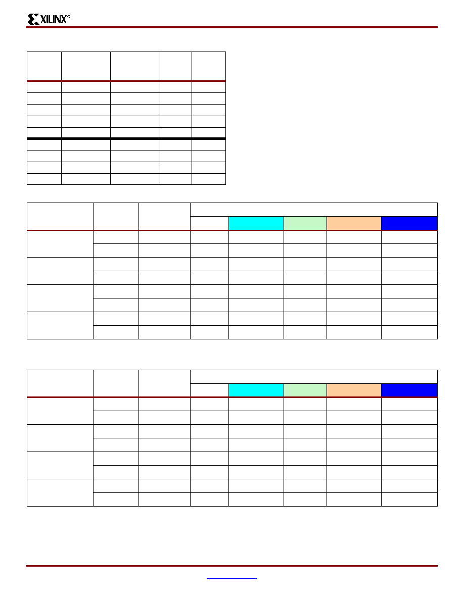
Spartan-3 1.2V FPGA Family: Pinout Descriptions
DS099-4 (v1.2.2) October 9, 2003
www.xilinx.com
93
Advance Product Specification
1-800-255-7778
R
User I/Os by Bank
Table 36
indicates how the available user-I/O pins are dis-
tributed between the eight I/O banks for the XC3S4000 in
the FG1156 package. Similarly,
Table 37
shows how the
available user-I/O pins are distributed between the eight I/O
banks for the XC3S5000 in the FG1156 package.
VCCAUX HSWAP_EN
HSWAP_EN
L11
CONFIG
VCCAUX M0
M0
AL4
CONFIG
VCCAUX M1
M1
AK4
CONFIG
VCCAUX M2
M2
AG8
CONFIG
VCCAUX PROG_B
PROG_B
D4
CONFIG
VCCAUX TCK
TCK
D31
JTAG
VCCAUX TDI
TDI
E4
JTAG
VCCAUX TDO
TDO
E31
JTAG
VCCAUX TMS
TMS
H27
JTAG
Table 35: FG1156 Package Pinout (Continued)
Bank
XC3S4000
Pin Name
XC3S5000
Pin Name
FG1156
Pin
Number
Type
Table 36: User I/Os Per Bank for XC3S4000 in FG1156 Package
Package Edge
I/O
Bank
Maximum
I/O
All Possible I/O Pins by Type
I/O
DUAL
DCI
VREF
GCLK
Top
0
90
79
0
2
7
2
1
90
79
0
2
7
2
Right
2
88
80
0
2
6
0
3
88
79
0
2
7
0
Bottom
4
90
73
6
2
7
2
5
90
73
6
2
7
2
Left
6
88
79
0
2
7
0
7
88
79
0
2
7
0
Table 37: User I/Os Per Bank for XC3S5000 in FG1156 Package
Package Edge
I/O
Bank
Maximum
I/O
All Possible I/O Pins by Type
I/O
DUAL
DCI
VREF
GCLK
Top
0
100
89
0
2
7
2
1
100
89
0
2
7
2
Right
2
96
87
0
2
7
0
3
96
87
0
2
7
0
Bottom
4
100
83
6
2
7
2
5
100
83
6
2
7
2
Left
6
96
87
0
2
7
0
7
96
87
0
2
7
0
Spartan-3 1.2V FPGA Family: Pinout Descriptions
94
www.xilinx.com
DS099-4 (v1.2.2) October 9, 2003
1-800-255-7778
Advance Product Specification
R
FG1156 Footprint
Top Left Corner of
Package (top view)
XC3S4000
(712 max. user I/O)
621
I/O: Unrestricted,
general-purpose user I/O
55
VREF: User I/O or input voltage
reference for bank
73
N.C.: Unconnected pins for
XC3S4000 (
)
XC3S5000
(784 max. user I/O)
692
I/O: Unrestricted,
general-purpose user I/O
56
VREF: User I/O or input voltage
reference for bank
1
N.C.: Unconnected pins for
XC3S5000 ( )
Figure 15: FG1156 Package Footprint (top view)
GND
GND
GND
GND
GND
GND
GND
GND
GND
GND
GND
GND
GND
GND
GND
GND
GND
GND
GND
GND
GND
GND
GND
GND
GND
GND
GND
GND
GND
GND
GND
GND
GND
GND
GND
GND
GND
GND
GND
GND
GND
GND
GND
GND
GND
GND
I/O
L01P_0
VRN_0
I/O
L02P_0
I/O
L05P_0
VREF_0
I/O
L34P_0
I/O
L36P_0
I/O
L38P_0
I/O
L40P_0
I/O
L15P_0
I/O
L22P_0
I/O
L26P_0
VREF_0
I/O
L32P_0
GCLK6
I/O
L01N_0
VRP_0
I/O
L02N_0
I/O
L03P_0
I/O
L05N_0
I/O
L34N_0
I/O
L36N_0
I/O
I/O
L38N_0
I/O
L40N_0
I/O
L15N_0
VCCO_0
I/O
L22N_0
I/O
L26N_0
I/O
L28P_0
I/O
L32N_0
GCLK7
I/O
L01N_7
VRP_7
I/O
L01P_7
VRN_7
VCCO_0
I/O
L03N_0
I/O
L04P_0
I/O
L33P_0 VCCO_0
I/O
L08P_0
I/O
L37P_0
I/O
L14P_0
I/O
L17P_0
I/O
L21P_0
I/O
L25P_0
I/O
L28N_0
I/O
L31P_0
VREF_0
I/O
L02N_7
I/O
L02P_7
VCCO_7 PROG_B
IO
VREF_0
I/O
L04N_0
I/O
L33N_0
I/O
L35P_0
I/O
L08N_0
I/O
L37N_0
VCCO_0
I/O
L14N_0
I/O
L17N_0
I/O
L21N_0
I/O
L25N_0
VCCO_0
I/O
L31N_0
I/O
L03N_7
VREF_7
I/O
L03P_7
TDI
VCCAUX
I/O
L06P_0
I/O
L35N_0
IO
VREF_0
VCCAUX
I/O
L13P_0
I/O
L20P_0
VCCAUX
I/O
I/O
L05N_7
I/O
L05P_7
I/O
L04N_7
I/O
L04P_7
VCCAUX
I/O
I/O
L06N_0
I/O
I/O
L07P_0
I/O
L10P_0
I/O
L39P_0
I/O
L13N_0
VCCO_0
I/O
L20N_0
I/O
L24P_0
I/O
L27P_0
I/O
L30P_0
I/O
I/O
I/O
L41N_7
I/O
L41P_7
I/O
L06N_7
I/O
L06P_7
VCCO_0
I/O
L07N_0
I/O
L10N_0
I/O
L39N_0
I/O
I/O
L16P_0
I/O
L19P_0
I/O
L24N_0
I/O
L27N_0
I/O
L30N_0
I/O
L08N_7
I/O
L08P_7
VCCO_7
I/O
L10P_7
VREF_7
I/O
L07N_7
I/O
L07P_7
VCCO_7
I/O
I/O
I/O
L09P_0
VCCO_0
I/O
L12P_0
I/O
L16N_0
I/O
L19N_0
VCCO_0 VCCAUX
I/O
L29P_0
I/O
L11N_7
I/O
L11P_7
I/O
L10N_7
I/O
L09N_7
I/O
L09P_7
I/O
L12P_7
I/O
I/O
L09N_0
I/O
I/O
L12N_0
IO
VREF_0
I/O
L23P_0
I/O
L29N_0
I/O
L16N_7
I/O
L16P_7
VREF_7
I/O
L15N_7
I/O
L15P_7
I/O
L14N_7
I/O
L14P_7
I/O
L13N_7
I/O
L13P_7
I/O
L12N_7
I/O
I/O
L11P_0
I/O
I/O
L18P_0
I/O
L23N_0
I/O
I/O
I/O
L19N_7
VREF_7
I/O
L19P_7
VCCO_7 VCCAUX
I/O
L44N_7
I/O
L44P_7 VCCO_7
I/O
L17N_7
I/O
L17P_7
HSWAP_
EN
I/O
L11N_0
I/O
I/O
L18N_0
IO
VREF_0
I/O
I/O
I/O
L45N_7
I/O
L45P_7
I/O
L23N_7
I/O
L23P_7
I/O
L22N_7
I/O
L22P_7
I/O
L21N_7
I/O
L21P_7
I/O
L24P_7
I/O
L20N_7
I/O
L20P_7
VCCINT
VCCO_0
VCCO_0
VCCO_0
VCCO_0
VCCINT
VCCO_7
I/O
L25N_7
I/O
L25P_7
VCCO_7
I/O
L46N_7
I/O
L46P_7
I/O
L24N_7
I/O
L26P_7
VCCO_7
VCCINT
VCCINT
VCCINT
VCCINT
I/O
L49N_7
I/O
L49P_7
I/O
L29N_7
I/O
L29P_7
I/O
L28N_7
I/O
L28P_7
I/O
L27N_7
I/O
L27P_7
VREF_7
I/O
L47N_7
I/O
L47P_7
I/O
L26N_7
VCCO_7
VCCINT
I/O
L32N_7
I/O
L32P_7
I/O
L31N_7
I/O
L31P_7
VCCAUX
I/O
L30N_7
I/O
L30P_7
VCCO_7
I/O
L33P_7
I/O
L50N_7
I/O
L50P_7
VCCO_7
VCCINT
I/O
L35N_7
I/O
L35P_7
VCCO_7
I/O
L34N_7
I/O
L34P_7
VCCAUX
I/O
L33N_7
I/O
L51P_7 VCCO_7
VCCINT
I/O
L40N_7
VREF_7
I/O
L40P_7
I/O
L39N_7
I/O
L39P_7
I/O
L38N_7
I/O
L38P_7
I/O
L37N_7
I/O
L37P_7
VREF_7
I/O
I/O
I/O
L51N_7
VCCINT
10
11
12
13
14
15
16
17
1
2
3
4
5
6
7
8
9
Bank 0
A
B
C
D
E
F
G
H
J
K
L
M
N
P
R
T
U
Bank 7
DS099-4_14a_072903

Spartan-3 1.2V FPGA Family: Pinout Descriptions
DS099-4 (v1.2.2) October 9, 2003
www.xilinx.com
95
Advance Product Specification
1-800-255-7778
R
All Devices
Top Right Corner of
Package (top view)
12
DUAL: Configuration pin, then
possible user I/O
16
DCI: User I/O or reference
resistor input for bank
8
GCLK: User I/O or global clock
buffer input
7
CONFIG: Dedicated
configuration pins
4
JTAG: Dedicated JTAG port
pins
104
VCCO: Output voltage supply
for bank
40
VCCINT: Internal core voltage
supply (+1.2V)
32
VCCAUX: Auxiliary voltage
supply (+2.5V)
184
GND: Ground
18
19
20
21
22
23
24
25
26
27
28
29
30
31
32
33
34
Bank 1
A
B
C
D
E
F
G
H
J
K
L
M
N
P
R
T
U
Bank 2
I/O
I/O
L40N_1
I/O
L26N_1
I/O
L19N_1
I/O
L15N_1
I/O
L14N_1
I/O
L08N_1
I/O
L34N_1
I/O
L05N_1
I/O
L02N_1
I/O
L01N_1
VRP_1
I/O
L32N_1
GCLK5
I/O
L28N_1
I/O
L40P_1
I/O
L26P_1
VCCO_1
I/O
L19P_1
I/O
L15P_1
I/O
L14P_1
I/O
I/O
L08P_1
I/O
L34P_1
I/O
L05P_1
I/O
L03N_1
I/O
L02P_1
I/O
L01P_1
VRN_1
I/O
L32P_1
GCLK4
I/O
L28P_1
I/O
L39N_1
I/O
L25N_1
I/O
L22N_1
I/O
I/O
L13N_1
I/O
L10N_1
VREF_1
VCCO_1
I/O
L33N_1
I/O
L04N_1
I/O
L03P_1
VCCO_1
I/O
L01N_2
VRP_2
I/O
L01P_2
VRN_2
I/O
L31N_1
VREF_1
VCCO_1
I/O
L39P_1
I/O
L25P_1
I/O
L22P_1
I/O
L18N_1
VCCO_1
I/O
L13P_1
I/O
L10P_1
I/O
L07N_1
I/O
L33P_1
I/O
L04P_1
IO
VREF_1
VCCO_2
I/O
L02N_2
I/O
L02P_2
I/O
L31P_1
VCCAUX
I/O
I/O
L18P_1
VCCAUX
I/O
I/O
L07P_1
I/O
L06N_1
VREF_1
VCCAUX
GND
GND
GND
GND
GND
GND
GND
GND
GND
GND
GND
GND
GND
GND
GND
GND
GND
GND
GND
GND
GND
GND
GND
GND
GND
GND
GND
GND
GND
GND
GND
GND
GND
GND
GND
GND
GND
GND
GND
GND
GND
GND
GND
GND
GND
GND
TDO
TCK
I/O
L03N_2
VREF_2
I/O
L03P_2
I/O
I/O
L27N_1
I/O
L38N_1
I/O
L24N_1
VCCO_1
I/O
L17N_1
VREF_1
I/O
L36N_1
I/O
L12N_1
I/O
L09N_1
I/O
I/O
L06P_1
I/O
VCCAUX
I/O
L04N_2
I/O
L04P_2
I/O
L41N_2
I/O
L41P_2
I/O
L30N_1
I/O
L27P_1
I/O
L38P_1
I/O
L24P_1
I/O
L21N_1
I/O
L17P_1
I/O
L36P_1
I/O
L12P_1
I/O
L09P_1
VCCO_1
I/O
L05N_2
I/O
L05P_2
I/O
L42N_2
I/O
L42P_2
I/O
I/O
I/O
L30P_1
VCCAUX VCCO_1
I/O
L23N_1
I/O
L21P_1
I/O
VCCO_1
I/O
L11N_1
I/O
TMS
VCCO_2
I/O
L06N_2
I/O
L06P_2
I/O
L09N_2
VREF_2
VCCO_2
I/O
L07N_2
I/O
L07P_2
I/O
L29N_1
I/O
L37N_1
I/O
L23P_1
I/O
L16N_1
I/O
L35N_1
I/O
L11P_1
I/O
I/O
L11N_2
I/O
L08N_2
I/O
L08P_2
I/O
L09P_2
I/O
L10N_2
I/O
L10P_2
I/O
L29P_1
I/O
I/O
L37P_1
IO
VREF_1
I/O
L20N_1
I/O
L16P_1
I/O
L35P_1
I/O
L11P_2
I/O
L12N_2
I/O
L12P_2
I/O
L13N_2
I/O
L13P_2
VREF_2
I/O
L14N_2
I/O
L14P_2
I/O
L15N_2
I/O
L15P_2
IO
VREF_1
I/O
I/O
I/O
I/O
L20P_1
I/O
I/O
I/O
L16N_2
I/O
L16P_2
VCCO_2
I/O
L17N_2
I/O
L17P_2
VREF_2 VCCAUX VCCO_2
I/O
L45N_2
I/O
L45P_2
VCCINT
VCCO_1
VCCO_1
VCCO_1
VCCO_1
VCCINT
I/O
L46N_2
I/O
L46P_2
I/O
L21N_2
I/O
L47N_2
I/O
L47P_2
I/O
L19N_2
I/O
L19P_2
I/O
L20N_2
I/O
L20P_2
I/O
L48N_2
I/O
L48P_2
VCCINT
VCCINT
VCCINT
VCCINT
VCCO_2
I/O
L24N_2
I/O
L21P_2
I/O
L22N_2
I/O
L22P_2
VCCO_2
I/O
L23N_2
VREF_2
I/O
L23P_2
VCCO_2
VCCINT
VCCO_2
I/O
L24P_2
I/O
L49N_2
I/O
L49P_2
I/O
L50N_2
I/O
L50P_2
I/O
L26N_2
I/O
L26P_2
I/O
L27N_2
I/O
L27P_2
I/O
L28N_2
I/O
L28P_2
VCCINT
VCCO_2
I/O
L29N_2
I/O
L29P_2
I/O
L33N_2
VCCO_2
I/O
L30N_2
I/O
L30P_2
VCCAUX
I/O
L31N_2
I/O
L31P_2
I/O
L32N_2
I/O
L32P_2
VCCINT
VCCO_2
I/O
L51N_2
I/O
L33P_2
VCCAUX
I/O
L34N_2
VREF_2
I/O
L34P_2
VCCO_2
I/O
L35N_2
I/O
L35P_2
VCCINT
I/O
L51P_2
I/O
I/O
I/O
L37N_2
I/O
L37P_2
I/O
L38N_2
I/O
L38P_2
I/O
L39N_2
I/O
L39P_2
I/O
L40N_2
I/O
L40P_2
VREF_2
DS099-4_14b_072903
Spartan-3 1.2V FPGA Family: Pinout Descriptions
96
www.xilinx.com
DS099-4 (v1.2.2) October 9, 2003
1-800-255-7778
Advance Product Specification
R
Bottom Left Corner of
Package (top view)
I/O
L40P_6
VREF_6
I/O
L40N_6
I/O
L39P_6
I/O
L39N_6
I/O
L38P_6
I/O
L38N_6
I/O
L52P_6
I/O
L52N_6
I/O
I/O
I/O
L49P_6
VCCINT
I/O
L37P_6
I/O
L37N_6
VCCO_6
I/O
L36P_6
I/O
L36N_6
VCCAUX
I/O
L35P_6
I/O
L49N_6 VCCO_6
VCCINT
I/O
L34P_6
I/O
L34N_6
VREF_6
I/O
L33P_6
I/O
L33N_6
VCCAUX
I/O
L48P_6
I/O
L48N_6
VCCO_6
I/O
L35N_6
I/O
L32P_6
I/O
L32N_6
VCCO_6
VCCINT
I/O
L31P_6
I/O
L31N_6
I/O
L30P_6
I/O
L30N_6
I/O
L29P_6
I/O
L29N_6
I/O
L28P_6
I/O
L28N_6
I/O
L46P_6
I/O
L46N_6
I/O
L27P_6
VCCO_6
VCCINT
VCCO_6
I/O
L26P_6
I/O
L26N_6
VCCO_6
I/O
L25P_6
I/O
L25N_6
I/O
L24P_6
I/O
L27N_6
VCCO_6
VCCINT
VCCINT
VCCINT
VCCINT
I/O
L23P_6
I/O
L23N_6
I/O
L45P_6
I/O
L45N_6
I/O
L22P_6
I/O
L22N_6
I/O
L21P_6
I/O
L21N_6
I/O
L24N_6
VREF_6
I/O
L20P_6
I/O
L20N_6
VCCINT
VCCO_5
VCCO_5
VCCO_5
VCCO_5
VCCINT
I/O
L19P_6
I/O
L19N_6
VCCO_6 VCCAUX
I/O
L44P_6
I/O
L44N_6 VCCO_6
I/O
L17P_6
VREF_6
I/O
L17N_6
I/O
I/O
I/O
L16P_5
I/O
I/O
I/O
I/O
I/O
L16P_6
I/O
L16N_6
I/O
L15P_6
I/O
L15N_6
I/O
L14P_6
I/O
L14N_6
I/O
L13P_6
VREF_6
I/O
L13N_6
I/O
L12P_6
I/O
L39P_5
I/O
L12P_5
I/O
L16N_5
I/O
I/O
L23P_5
I/O
I/O
L29P_5
VREF_5
I/O
L11P_6
I/O
L11N_6
I/O
L10P_6
I/O
L09P_6
I/O
L09N_6
VREF_6
I/O
L12N_6
I/O
I/O
L07P_5
I/O
L39N_5
I/O
L12N_5
I/O
L19P_5
VREF_5
I/O
L23N_5
I/O
L29N_5
I/O
L08P_6
I/O
L08N_6
VCCO_6
I/O
L10N_6
I/O
L07P_6
I/O
L07N_6
VCCO_6
M2
I/O
I/O
L07N_5
VCCO_5
I/O
I/O
L17P_5
I/O
L19N_5
VCCO_5 VCCAUX
I/O
L30P_5
I/O
I/O
I/O
L41P_6
I/O
L41N_6
I/O
L06P_6
I/O
L06N_6
VCCO_5
I/O
L37P_5
I/O
L08P_5
I/O
L40P_5
I/O
L13P_5
I/O
L17N_5
I/O
L20P_5
I/O
L24P_5
I/O
L27P_5
I/O
L30N_5
I/O
L05P_6
I/O
L05N_6
I/O
L04P_6
I/O
L04N_6
VCCAUX
I/O
I/O
L06P_5
IO
VREF_5
I/O
L37N_5
I/O
L08N_5
I/O
L40N_5
I/O
L13N_5
VCCO_5
I/O
L20N_5
I/O
L24N_5
I/O
L27N_5
VREF_5
I/O
I/O
L03P_6
I/O
L03N_6
VREF_6
M1
VCCAUX
I/O
L06N_5
I/O
L35P_5
I/O
VCCAUX
I/O
L14P_5
I/O
VCCAUX
I/O
L31P_5
D5
I/O
L02P_6
I/O
L02N_6
VCCO_6
M0
IO
VREF_5
I/O
L04P_5
I/O
L33P_5
I/O
L35N_5
I/O
L38P_5
I/O
L09P_5
VCCO_5
I/O
L14N_5
I/O
L18P_5
I/O
L21P_5
I/O
L25P_5
VCCO_5
I/O
L31N_5
D4
I/O
L01P_6
VRN_6
I/O
L01N_6
VRP_6
VCCO_5
I/O
L03P_5
I/O
L04N_5
I/O
L33N_5 VCCO_5
I/O
L38N_5
I/O
L09N_5
I/O
I/O
L18N_5
I/O
L21N_5
I/O
L25N_5
I/O
L28P_5
D7
I/O
L32P_5
GCLK2
I/O
L01P_5
CS_B
I/O
L02P_5
I/O
L03N_5
I/O
L05P_5
I/O
L34P_5
I/O
L36P_5
I/O
I/O
L10P_5
VRN_5
I/O
L11P_5
I/O
L15P_5
VCCO_5
I/O
L22P_5
I/O
L26P_5
I/O
L28N_5
D6
I/O
L32N_5
GCLK3
I/O
L01N_5
RDWR_B
I/O
L02N_5
GND
GND
GND
GND
GND
GND
GND
GND
GND
GND
GND
GND
GND
GND
GND
GND
GND
GND
GND
GND
GND
GND
GND
GND
GND
GND
GND
GND
GND
GND
GND
GND
GND
GND
GND
GND
GND
GND
GND
GND
GND
GND
GND
GND
GND
GND
I/O
L05N_5
I/O
L34N_5
I/O
L36N_5
I/O
L10N_5
VRP_5
I/O
L11N_5
VREF_5
I/O
L15N_5
I/O
L22N_5
I/O
L26N_5
IO
VREF_5
Bank 5
10
11
12
13
14
15
16
17
V
W
Y
A
A
A
B
A
C
A
D
A
E
A
F
A
G
A
H
A
J
A
K
A
L
A
M
A
N
A
P
Bank 6
1
2
3
4
5
6
7
8
9
DS099-4_14c_072503
Spartan-3 1.2V FPGA Family: Pinout Descriptions
DS099-4 (v1.2.2) October 9, 2003
www.xilinx.com
97
Advance Product Specification
1-800-255-7778
R
Bottom Right Corner
of Package (top view)
VCCINT
I/O
L51N_3
I/O
I/O
I/O
L37P_3
I/O
L37N_3
I/O
L38P_3
I/O
L38N_3
I/O
L39P_3
I/O
L39N_3
I/O
L40P_3
I/O
L40N_3
VREF_3
VCCINT
VCCO_3
I/O
L51P_3
I/O
L33N_3
VCCAUX
I/O
L34P_3
VREF_3
I/O
L34N_3
VCCO_3
I/O
L35P_3
I/O
L35N_3
VCCINT
VCCO_3
I/O
L50P_3
I/O
L50N_3
I/O
L33P_3
VCCO_3
I/O
L30P_3
I/O
L30N_3
VCCAUX
I/O
L31P_3
I/O
L31N_3
I/O
L32P_3
I/O
L32N_3
VCCINT
VCCO_3
I/O
L48N_3
I/O
L49P_3
I/O
L49N_3
I/O
L26P_3
I/O
L26N_3
I/O
L27P_3
I/O
L27N_3
I/O
L28P_3
I/O
L28N_3
I/O
L29P_3
I/O
L29N_3
VCCINT VCCINT
VCCINT
VCCINT
VCCO_3
I/O
L48P_3
I/O
L24N_3
I/O
L46P_3
I/O
L46N_3
VCCO_3
I/O
L47P_3
I/O
L47N_3
VCCO_3
VCCINT
VCCO_4
VCCO_4
VCCO_4
VCCO_4
VCCINT
I/O
L20P_3
I/O
L20N_3
I/O
L24P_3
I/O
L21P_3
I/O
L21N_3
I/O
L22P_3
I/O
L22N_3
I/O
L23P_3
VREF_3
I/O
L23N_3
I/O
L45P_3
I/O
L45N_3
I/O
I/O
I/O
I/O
L18N_4
I/O
I/O
L11N_4
DONE
I/O
L17P_3
VREF_3
I/O
L17N_3
VCCO_3
I/O
L44P_3
I/O
L44N_3
VCCO_3
I/O
L19P_3
I/O
L19N_3
I/O
I/O
I/O
L23N_4
I/O
L18P_4
I/O
I/O
L11P_4
I/O
I/O
L12N_3
I/O
L13P_3
I/O
L13N_3
VREF_3
I/O
L14P_3
I/O
L14N_3
I/O
L15P_3
I/O
L15N_3
I/O
L16P_3
I/O
L16N_3
I/O
L29N_4
I/O
L23P_4
IO
VREF_4
I/O
L12N_4
I/O
I/O
L07N_4
I/O
I/O
L12P_3
I/O
L09P_3
VREF_3
I/O
L09N_3
I/O
L10N_3
I/O
L11P_3
I/O
L11N_3
I/O
L29P_4
VCCAUX VCCO_4
I/O
L19N_4
I/O
L16N_4
I/O
L12P_4
VCCO_4
I/O
L07P_4
I/O
I/O
VCCO_3
I/O
L07P_3
I/O
L07N_3
I/O
L10P_3
VCCO_3
I/O
L08P_3
I/O
L08N_3
I/O
L30N_4
D2
I/O
L27N_4
DIN
D0
I/O
L24N_4
I/O
L19P_4
I/O
L16P_4
IO
VREF_4
I/O
L39N_4
I/O
L08N_4
I/O
L05N_4
VCCO_4
I/O
L06P_3
I/O
L06N_3
I/O
L41P_3
I/O
L41N_3
I/O
I/O
I/O
L30P_4
D3
I/O
L27P_4
D1
I/O
L24P_4
I/O
L20N_4
VCCO_4
I/O
L13N_4
I/O
L39P_4
I/O
L08P_4
I/O
L05P_4
I/O
I/O
L35N_4
I/O
VCCAUX
I/O
L04P_3
I/O
L04N_3
I/O
L05P_3
I/O
L05N_3
IO
VREF_4
VCCAUX
I/O
L20P_4
I/O
L13P_4
VCCAUX
I/O
I/O
L38N_4
I/O
L35P_4
VCCAUX
N.C.
I/O
L03P_3
I/O
L03N_3
I/O
L31N_4
INIT_B
VCCO_4
I/O
L25N_4
I/O
L21N_4
I/O
L17N_4
I/O
L14N_4
VCCO_4
I/O
L09N_4
I/O
L06N_4
VREF_4
I/O
L38P_4
I/O
L36N_4
I/O
L33N_4
IO
VREF_4
CCLK
VCCO_3
I/O
L02P_3
I/O
L02N_3
VREF_3
I/O
L31P_4
DOUT
BUSY
I/O
L28N_4
I/O
L25P_4
I/O
L21P_4
I/O
L17P_4
I/O
L14P_4
I/O
L09P_4
I/O
L06P_4
VCCO_4
I/O
L36P_4
I/O
L33P_4
I/O
L03N_4
VCCO_4
I/O
L01P_3
VRN_3
I/O
L01N_3
VRP_3
I/O
L32N_4
GCLK1
I/O
L28P_4
I/O
L26N_4
I/O
L22N_4
VREF_4
VCCO_4
I/O
L15N_4
I/O
L40N_4
I/O
L10N_4
I/O
I/O
L04N_4
I/O
L37N_4
I/O
L34N_4
I/O
L03P_4
I/O
L02N_4
I/O
L01N_4
VRP_4
I/O
L32P_4
GCLK0
I/O
L26P_4
VREF_4
I/O
L22P_4
I/O
L15P_4
I/O
L40P_4
I/O
L10P_4
I/O
L04P_4
I/O
L37P_4
I/O
L34P_4
I/O
L02P_4
I/O
L01P_4
VRN_4
GND
GND
GND
GND
GND
GND
GND
GND
GND
GND
GND
GND
GND
GND
GND
GND
GND
GND
GND
GND
GND
GND
GND
GND
GND
GND
GND
GND
GND
GND
GND
GND
GND
GND
GND
GND
GND
GND
GND
GND
GND
GND
GND
GND
GND
GND
18
19
20
21
22
23
24
25
26
27
28
29
30
31
32
33
34
Bank 4
V
W
Y
A
A
A
B
A
C
A
D
A
E
A
F
A
G
A
H
A
J
A
K
A
L
A
M
A
N
A
P
Bank 3
DS099-4_14d_072903
VCCAUX
Spartan-3 1.2V FPGA Family: Pinout Descriptions
98
www.xilinx.com
DS099-4 (v1.2.2) October 9, 2003
1-800-255-7778
Advance Product Specification
R
Revision History
The Spartan-3 Family Data Sheet
DS099-1, Spartan-3 1.2V FPGA Family:
Introduction and Ordering Information
(Module 1)
DS099-2, Spartan-3 1.2V FPGA Family:
Functional Description
(Module 2)
DS099-3, Spartan-3 1.2V FPGA Family:
DC and Switching Characteristics
(Module 3)
DS099-4, Spartan-3 1.2V FPGA Family: Pinout Descriptions (Module 4)
Date
Version No.
Description
04/03/03
1.0
Initial Xilinx release.
04/21/03
1.1
Added information on the VQ100 package footprint, including a complete pinout table
(
Table 16
) and footprint diagram (
Figure 8
).
Updated
Table 15
with final I/O counts for the VQ100 package. Also added final differential I/O
pair counts for the TQ144 package.
Added clarifying comments to HSWAP_EN pin description on
page 13
.
Updated the footprint diagram for the FG900 package shown in
Figure 14a
and
Figure 14b
.
Some thick lines separating I/O banks were incorrect.
Made cosmetic changes to
Figure 1
,
Figure 3
, and
Figure 4
.
Updated Xilinx hypertext links.
Added XC3S200 and XC3S400 to Pin Name column in
Table 18
.
05/12/03
1.1.1
AM32 pin was missing GND label in FG1156 package diagram (
Figure 15
).
07/11/03
1.1.2
Corrected misspellings of GCLK in
Table 1
and
Table 2
. Changed CMOS25 to LVCMOS25 in
Dual-Purpose Pin I/O Standard During Configuration
section. Clarified references to
Module 2. For XC3S5000 in FG1156 package, corrected N.C. symbol to a black square in
Table 35
, key, and package drawing.
07/29/03
1.2
Corrected pin names on FG1156 package. Some package balls incorrectly included LVDS pair
names. The affected balls on the FG1156 package include G1, G2, G33, G34, U9, U10, U25,
U26, V9, V10, V25, V26, AH1, AH2, AH33, AH34. The number of LVDS pairs is unaffected.
Modified affected balls and re-sorted rows in
Table 35
. Updated affected balls in
Figure 15
.
Also updated ASCII and Excel electronic versions of FG1156 pinout.
08/19/03
1.2.1
Removed 100 MHz ConfigRate option in
CCLK: Configuration Clock
section and in
Table 11
.
Added note that TDO is a totem-pole output in
Table 9
.
10/09/03
1.2.2
Some pins had incorrect bank designations and were improperly sorted in
Table 20
. No pin
names or functions changed. Renamed DCI_IN to DCI and added black diamond to N.C. pins
in
Table 20
. In
Figure 10
, removed some extraneous text from pin 106 and corrected spelling
of pins 45, 48, and 81.