2-7
Device
XC4002A 4003/3A
4003H
4004A
4005/5A
4005H
4006
4008
4010/10D 4013/13D 4020
4025
Appr. Gate Count
2,000
3,000
3,000
4,000
5,000
5,000
6,000
8,000
10,000
13,000
20,000
25,000
CLB Matrix
8 x 8
10 x 10
10 x 10
12 x 12
14 x 14
14 x 14 16 x 16
18 x 18
20 x 20 24 x 24 28 x 28 32 x 32
Number of CLBs
64
100
100
144
196
196
256
324
400
576
784
1,024
Number of Flip-Flops
256
360
200
480
616
392
768
936
1,120
1,536
2,016
2,560
Max Decode Inputs
24
30
30
36
42
42
48
54
60
72
84
96
(per side)
Max RAM Bits
2,048
3,200
3,200
4,608
6,272
6,272
8,192
10,368
12,800* 18,432* 25,088
32,768
Number of IOBs
64
80
160
96
112
192
128
144
160
192
224
256
*XC4010D and XC4013D have no RAM
�
XC4000, XC4000A, XC4000H
Logic Cell Array Families
Product Description
Description
The XC4000 families of Field-Programmable Gate Arrays
(FPGAs) provide the benefits of custom CMOS VLSI, while
avoiding the initial cost, time delay, and inherent risk of a
conventional masked gate array.
The XC4000 families provide a regular, flexible, program-
mable architecture of Configurable Logic Blocks (CLBs),
interconnected by a powerful hierarchy of versatile routing
resources, and surrounded by a perimeter of program-
mable Input/Output Blocks (IOBs).
XC4000-family devices have generous routing resources to
accommodate the most complex interconnect patterns.
XC4000A devices have reduced sets of routing resources,
sufficient for their smaller size. XC4000H high I/O devices
maintain the same routing resources and CLB structure as
the XC4000 family, while nearly doubling the available I/O.
The devices are customized by loading configuration data
into the internal memory cells. The FPGA can either actively
read its configuration data out of external serial or byte-
parallel PROM (master modes), or the configuration data
can be written into the FPGA (slave and peripheral modes).
The XC4000 families are supported by powerful and so-
phisticated software, covering every aspect of design: from
schematic entry, to simulation, to automatic block place-
ment and routing of interconnects, and finally the creation
of the configuration bit stream.
Since Xilinx FPGAs can be reprogrammed an unlimited
number of times, they can be used in innovative designs
where hardware is changed dynamically, or where hard-
ware must be adapted to different user applications. FPGAs
are ideal for shortening the design and development cycle,
but they also offer a cost-effective solution for production
rates well beyond 1000 systems per month.
Features
�
Third Generation Field-Programmable Gate Arrays
� Abundant flip-flops
� Flexible function generators
� On-chip ultra-fast RAM
� Dedicated high-speed carry-propagation circuit
� Wide edge decoders
� Hierarchy of interconnect lines
� Internal 3-state bus capability
� Eight global low-skew clock or signal distribution
network
�
Flexible Array Architecture
� Programmable logic blocks and I/O blocks
� Programmable interconnects and wide decoders
�
Sub-micron CMOS Process
� High-speed logic and Interconnect
� Low power consumption
�
Systems-Oriented Features
� IEEE 1149.1-compatible boundary-scan logic support
� Programmable output slew rate
� Programmable input pull-up or pull-down resistors
� 12-mA sink current per output (XC4000 family)
� 24-mA sink current per output (XC4000A and
XC4000H families)
�
Configured by Loading Binary File
� Unlimited reprogrammability
� Six programming modes
�
XACT Development System runs on '386/'486-type PC,
NEC PC, Apollo, Sun-4, and Hewlett-Packard 700
series
� Interfaces to popular design environments like
Viewlogic, Mentor Graphics and OrCAD
� Fully automatic partitioning, placement and routing
� Interactive design editor for design optimization
� 288 macros, 34 hard macros, RAM/ROM compiler
Table 1. The XC4000 Families of Field-Programmable Gate Arrays
XC4000, XC4000A, XC4000H Logic Cell Array Families
2-8
XC4000 Compared to XC3000A
For those readers already familiar with the XC3000A
family of Xilinx Field Programmable Gate Arrays, here is a
concise list of the major new features in the XC4000 family.
CLB has two independent 4-input function generators.
A third function generator combines the outputs of the
two other function generators with a ninth input.
All function inputs are swappable, all have full access;
none are mutually exclusive.
CLB has very fast arithmetic carry capability.
CLB function generator look-up table can also be used as
high-speed RAM.
CLB flip-flops have asynchronous set or reset.
CLB has four outputs, two flip-flops, two combinatorial.
CLB connections symmetrically located on all four edges.
IOB has more versatile clocking polarity options.
IOB has programmable input set-up time:
long to avoid potential hold time problems,
short to improve performance.
IOB has Longline access through its own TBUF.
Outputs are n-channel only, lower V
OH
increases speed.
XC4000 outputs can be paired to double sink current to
24 mA. XC4000A and XC4000H outputs can each
sink 24 mA, can be paired for 48 mA sink current.
IEEE 1149.1- type boundary scan is supported in the I/O.
Wide decoders on all four edges of the LCA device.
Increased number of interconnect resources.
All CLB inputs and outputs have access to most inter-
connect lines.
Switch Matrices are simplified to increase speed.
Eight global nets can be used for clocking or distributing
logic signals.
TBUF output configuration is more versatile and 3-state
control less confined.
Program is single-function input pin,overrides everything.
INIT pin also acts as Configuration Error output.
Peripheral Synchronous Mode (8 bit) has been added.
Peripheral Asynchronous Mode has improved hand-
shake.
Start-up can be synchronized to any user clock (this is a
configuration option).
No Powerdown, but instead a Global 3-state input that
does not reset any flip-flops.
No on-chip crystal oscillator amplifier.
Configuration Bit Stream includes CRC error checking.
Configuration Clock can be increased to >8 MHz.
Configuration Clock is fully static, no constraint on the
maximum Low time.
Readback either ignores flip-flop content (avoids need for
masking) or it takes a snapshot of all flip-flops at the
start of Readback.
Readback has same polarity as Configuration and can be
aborted.
Table 2. Three Generations of Xilinx Field-Programmable Gate Array Families
Parameter
XC4025
XC3195A
XC2018
Number of flip-flops
2,560
1,320
174
Max number of user I/O
256
176
74
Max number of RAM bits
32,768
0
0
Function generators per CLB
3
2
2
Number of logic inputs per CLB
9
5
4
Number of logic outputs per CLB
4
2
2
Number of low-skew global nets
8
2
2
Dedicated decoders
yes
no
no
Fast carry logic
yes
no
no
Internal 3-state drivers
yes
yes
no
Output slew-rate control
yes
yes
no
Power-down option
no
yes
yes
Crystal oscillator circuit
no
yes
yes

2-9
Architectural Overview
The XC4000 families achieve high speed through ad-
vanced semiconductor technology and through improved
architecture, and supports system clock rates of up to 50
MHz. Compared to older Xilinx FPGA families, the XC4000
families are more powerful, offering on-chip RAM and
wide-input decoders. They are more versatile in their
applications, and design cycles are faster due to a combi-
nation of increased routing resources and more sophisti-
cated software. And last, but not least, they more than
double the available complexity, up to the 20,000-gate
level.
The XC4000 families have 16 members, ranging in com-
plexity from 2,000 to 25,000 gates.
Logic Cell Array Families
Xilinx high-density user-programmable gate arrays in-
clude three major configurable elements: configurable
logic blocks (CLBs), input/output blocks (IOBs), and inter-
connections. The CLBs provide the functional elements
for constructing the user's logic. The IOBs provide the
interface between the package pins and internal signal
lines. The programmable interconnect resources provide
routing paths to connect the inputs and outputs of the CLBs
and IOBs onto the appropriate networks. Customized
configuration is established by programming internal static
memory cells that determine the logic functions and inter-
connections implemented in the LCA device.
The first generation of LCA devices, the XC2000 family,
was introduced in 1985. It featured logic blocks consisting
of a combinatorial function generator capable of imple-
menting 4-input Boolean functions and a single storage
element. The XC2000 family has two members ranging in
complexity from 800 to 1500 gates.
In the second-generation XC3000A LCA devices, intro-
duced in 1987, the logic block was expanded to implement
wider Boolean functions and to incorporate a second flip-
flop in each logic block. Today, the XC3000 devices range
in complexity from 1,300 to 10,000 usable gates. They
have a maximum guaranteed toggle frequency ranging
from 70 to 270 MHz, equivalent to maximum system clock
frequencies of up to 80 MHz.
The third generation of LCA devices further extends this
architecture with a yet more powerful and flexible logic
block. I/O block functions and interconnection options
have also been enhanced with each successive genera-
tion, further extending the range of applications that can be
implemented with an LCA device.
This third-generation architecture forms the basis of the
XC4000 families of devices that feature logic densities up
to 25,000 usable gates and support system clock rates of
up to 50 MHz. The use of an advanced, sub-micron CMOS
process technology as well as architectural improvements
contribute to this increase in FPGA capabilities. However,
achieving these high logic-density and performance levels
also requires new and more powerful automated design
tools. IC and software engineers collaborated during the
definition of the third-generation LCA architecture to meet
an important performance goal -- an FPGA architecture
and companion design tools for completely automatic
placement and routing of 95% of all designs, plus a
convenient way to complete the remaining few designs.
Configurable Logic Blocks
A number of architectural improvements contribute to the
increased logic density and performance levels of the
XC4000 families. The most important one is a more
powerful and flexible CLB surrounded by a versatile set of
routing resources, resulting in more "effective gates per
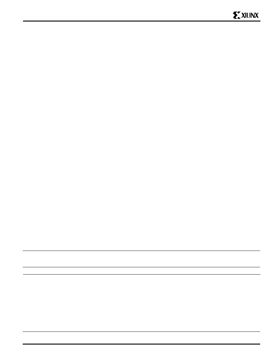
CLB." The principal CLB elements are shown in Figure 1.
Each new CLB also packs a pair of flip-flops and two
independent 4-input function generators. The two function
generators offer designers plenty of flexibility because
most combinatorial logic functions need less than four
inputs. Consequently, the design-software tools can deal
with each function generator independently, thus improv-
ing cell usage.
Thirteen CLB inputs and four CLB outputs provide access
to the function generators and flip-flops. More than double
the number available in the XC3000 families, these inputs
and outputs connect to the programmable interconnect
resources outside the block. Four independent inputs are
provided to each of two function generators (F1 � F4 and
G1 � G4). These function generators, whose outputs are
labeled F' and G', are each capable of implementing any
arbitrarily defined Boolean function of their four inputs. The
function generators are implemented as memory look-up
tables; therefore, the propagation delay is independent of
the function being implemented. A third function genera-
tor, labeled H', can implement any Boolean function of its
three inputs: F' and G' and a third input from outside the
block (H1). Signals from the function generators can exit
the CLB on two outputs; F' or H' can be connected to the
X output, and G' or H' can be connected to the Y output.
Thus, a CLB can be used to implement any two independ-
ent functions of up-to-four variables, or any single function
of five variables, or any function of four variables together
with some functions of five variables , or it can implement
even some functions of up to nine variables. Implementing
wide functions in a single block reduces both the number
of blocks required and the delay in the signal path, achiev-
ing both increased density and speed.
The two storage elements in the CLB are edge-triggered
D-type flip-flops with common clock (K) and clock enable
(EC) inputs. A third common input (S/R) can be pro-
grammed as either an asynchronous set or reset signal

XC4000, XC4000A, XC4000H Logic Cell Array Families
2-10
independently for each of the two registers; this input also
can be disabled for either flip-flop. A separate global Set/
Reset line (not shown in Figure 1) sets or clears each
register during power-up, reconfiguration, or when a dedi-
cated Reset net is driven active. This Reset net does not
compete with other routing resources; it can be connected
to any package pin as a global reset input.
Each flip-flop can be triggered on either the rising or falling
clock edge. The source of a flip-flop data input is program-
mable: it is driven either by the functions F', G', and H', or
the Direct In (DIN) block input . The flip-flops drive the XQ
and YQ CLB outputs.
In addition, each CLB F' and G' function generator con-
tains dedicated arithmetic logic for the fast generation of
carry and borrow signals, greatly increasing the efficiency
and performance of adders, subtracters, accumulators,
comparators and even counters.
Multiplexers in the CLB map the four control inputs, la-
beled C1 through C4 in Figure 1, into the four internal
control signals (H1, DIN, S/R, and EC) in any arbitrary
manner.
The flexibility and symmetry of the CLB architecture facili-
tates the placement and routing of a given application.
Since the function generators and flip-flops have inde-
pendent inputs and outputs, each can be treated as a
separate entity during placement to achieve high packing
density. Inputs, outputs, and the functions themselves can
freely swap positions within a CLB to avoid routing conges-
tion during the placement and routing operation.
Figure 1. Simplified Block Diagram of XC4000-Families Configurable Logic Block
LOGIC
FUNCTION
OF
G1-G4
G4
G3
G2
G1
G'
LOGIC
FUNCTION
OF
F1-F4
F4
F3
F2
F1
F'
LOGIC
FUNCTION
OF
F', G',
AND
H1
H'
DIN
F'
G'
H'
DIN
F'
G'
H'
G'
H'
H'
F'
S/R
CONTROL
D
EC
RD
SD
Q
YQ
S/R
CONTROL
D
EC
RD
SD
Q
XQ
1
1
K
(CLOCK)
Y
X
H1
DIN
S/R
EC
C1
C2
C3
C4
X6099
BYPASS
BYPASS
MULTIPLEXER CONTROLLED
BY CONFIGURATUON PROGRAM
2-11
Speed Is Enhanced Two Ways
Delays in LCA-based designs are layout dependent. While
this makes it hard to predict a worst-case guaranteed
performance, there is a rule of thumb designers can
consider -- the system clock rate should not exceed one
third to one half of the specified toggle rate. Critical
portions of a design, shift registers and simple counters,
can run faster -- approximately two thirds of the specified
toggle rate.
The XC4000 family can run at synchronous system clock
rates of up to 60 MHz. This increase in performance over
the previous families stems from two basic improve-
ments: improved architecture and more abundant routing
resources.
Improved Architecture
More Inputs: The versatility of the CLB function genera-
tors improves system speed significantly. Table 3 shows
how the XC4000 families implement many functions more
efficiently and faster than is possible with XC3000 devices.
A 9-bit parity checker, for example, can be implemented in
one CLB with a propagation delay of 7 ns. Using a
XC3000-family device, the same function requires two
CLBs with a propagation delay of 2 x 5.5 ns = 11 ns. One
XC4000 CLB can determine whether two 4-bit words are
identical, again with a 7-ns propagation delay. The ninth
input can be used for simple ripple expansion of this
identity comparator (25.5 ns over 16 bits, 51.5 ns over
32 bits), or a 2-layer identity comparator can generate the
result of a 32-bit comparison in 15 ns, at the cost of a single
extra CLB. Simpler functions like multiplexers also benefit
from the greater flexibility of the XC4000-families CLB. A
16-input multiplexer uses 5 CLBs and has a delay of only
13.5 ns.
More Outputs: The CLB can pass the combinatorial
output(s) to the interconnect network, but can also store
the combinatorial result(s) or other incoming data in one or
two flip-flops, and connect their outputs to the interconnect
network as well. With XC3000-families CLBs the designer
has to make a choice, either output the combinatorial
function or the stored value. In the XC4000 families, the flip
flops can be used as registers or shift registers without
blocking the function generators from performing a differ-
ent, perhaps unrelated task. This increases the functional
density of the devices.
When a function generator drives a flip-flop in a CLB, the
combinatorial propagation delay
overlaps completely with
the set-up time of the flip-flop. The set-up time is specified
between the function generator inputs and the clock input.
This represents a performance advantage over competing
technologies where combinatorial delays must be added
to the flip-flop set-up time.
Fast Carry: As described earlier, each CLB includes high-
speed carry logic that can be activated by configuration.
The two 4-input function generators can be configured as
a 2-bit adder with built-in hidden carry that can be ex-
panded to any length. This dedicated carry circuitry is so
fast and efficient that conventional speed-up methods like
carry generate/propagate are meaningless even at the
16-bit level, and of marginal benefit at the 32-bit level.
A 16-bit adder requires nine CLBs and has a combinatorial
carry delay of 20.5 ns. Compare that to the 30 CLBs and
50 ns, or 41 CLBs and 30 ns in the XC3000 family.
The fast-carry logic opens the door to many new applica-
tions involving arithmetic operation, where the previous
generations of FPGAs were not fast and/or not efficient
enough. High-speed address offset calculations in micro-
processor or graphics systems, and high-speed addition in
digital signal processing are two typical applications.
Faster and More Efficient Counters: The XC4000-fami-
lies fast-carry logic puts two counter bits into each CLB and
runs them at a clock rate of up to 42 MHz for 16 bits,
whether the counters are loadable or not. For a 16-bit
Table 3. Density and Performance for Several Common Circuit Functions
XC3000 (-125)
XC4000 (-5)
16-bit Decoder From Input Pad
15 ns
4 CLBs
12 ns
0 CLBs
24-bit Accumulator
17 MHz
46 CLBs
32 MHz
13 CLBs
State Machine Benchmark*
18 MHz
34 CLBs
30 MHz
26 CLBs
16:1 Multiplexer
16 ns
8 CLBs
16 ns
5 CLBs
16-bit Unidirectional
Max Density
20 MHz
16 CLBs
40 MHz
8 CLBs
Loadable Counter
Max Speed
34 MHz
23 CLBs
42 MHz
9 CLBs
16-bit U/D Counter
Max Density
20 MHz
16 CLBs
40 MHz
8 CLBs
Max Speed
30 MHz
27 CLBs
40 MHz
8 CLBs
16-bit Adder
Max Density
50 ns
30 CLBs
20.5 ns
9 CLBs
Max Speed
30 ns
41 CLBs
20.5 ns
9 CLBs
* 16 states, 40 transitions, 10 inputs, 8 outputs