May 14, 1999 (Version 1.6)
6-5
6
XC4000E and XC4000X Series
Features
Note: Information in this data sheet covers the XC4000E,
XC4000EX, and XC4000XL families. A separate data sheet
covers the XC4000XLA and XC4000XV families. Electrical
Specifications and package/pin information are covered in
separate sections for each family to make the information
easier to access, review, and print. For access to these sec-
tions, see the Xilinx W
EB
LINX web site at
http://www.xilinx.com/partinfo/databook.htm#xc4000
.
∑
System featured Field-Programmable Gate Arrays
-
Select-RAM
TM
memory: on-chip ultra-fast RAM with
-
synchronous write option
-
dual-port RAM option
-
Fully PCI compliant (speed grades -2 and faster)
-
Abundant flip-flops
-
Flexible function generators
-
Dedicated high-speed carry logic
-
Wide edge decoders on each edge
-
Hierarchy of interconnect lines
-
Internal 3-state bus capability
-
Eight global low-skew clock or signal distribution
networks
∑
System Performance beyond 80 MHz
∑
Flexible Array Architecture
∑
Low Power Segmented Routing Architecture
∑
Systems-Oriented Features
-
IEEE 1149.1-compatible boundary scan logic
support
-
Individually programmable output slew rate
-
Programmable input pull-up or pull-down resistors
-
12 mA sink current per XC4000E output
∑
Configured by Loading Binary File
-
Unlimited re-programmability
∑
Read Back Capability
-
Program verification
-
Internal node observability
∑
Backward Compatible with XC4000 Devices
∑
Development System runs on most common computer
platforms
-
Interfaces to popular design environments
-
Fully automatic mapping, placement and routing
-
Interactive design editor for design optimization
Low-Voltage Versions Available
∑
Low-Voltage Devices Function at 3.0 - 3.6 Volts
∑
XC4000XL: High Performance Low-Voltage Versions of
XC4000EX devices
Additional XC4000X Series Features
∑
Highest Performance -- 3.3 V XC4000XL
∑
Highest Capacity -- Over 180,000 Usable Gates
∑
5 V tolerant I/Os on XC4000XL
∑
0.35
µ
m SRAM process for XC4000XL
∑
Additional Routing Over XC4000E
-
almost twice the routing capacity for high-density
designs
∑
Buffered Interconnect for Maximum Speed Blocks
∑
Improved VersaRing
TM
I/O Interconnect for Better Fixed
Pinout Flexibility
∑
12 mA Sink Current Per XC4000X Output
∑
Flexible New High-Speed Clock Network
-
Eight additional Early Buffers for shorter clock delays
-
Virtually unlimited number of clock signals
∑
Optional Multiplexer or 2-input Function Generator on
Device Outputs
∑
Four Additional Address Bits in Master Parallel
Configuration Mode
∑
XC4000XV Family offers the highest density with
0.25
µ
m 2.5 V technology
Introduction
XC4000 Series high-performance, high-capacity Field Pro-
grammable Gate Arrays (FPGAs) provide the benefits of
custom CMOS VLSI, while avoiding the initial cost, long
development cycle, and inherent risk of a conventional
masked gate array.
The result of thirteen years of FPGA design experience and
feedback from thousands of customers, these FPGAs com-
bine architectural versatility, on-chip Select-RAM memory
with edge-triggered and dual-port modes, increased
speed, abundant routing resources, and new, sophisticated
software to achieve fully automated implementation of
complex, high-density, high-performance designs.
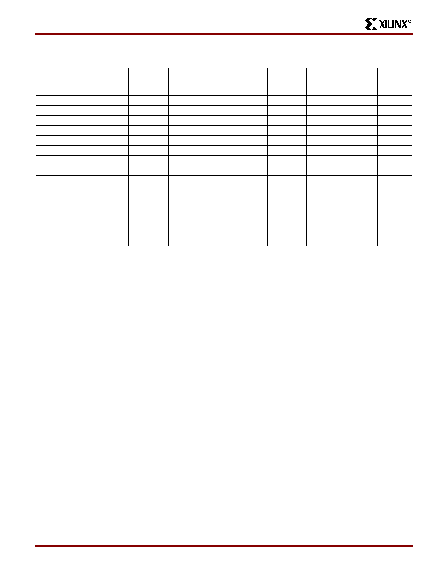
The XC4000E and XC4000X Series currently have 20
members, as shown in
Table 1
.
0
XC4000E and XC4000X Series Field
Programmable Gate Arrays
May 14, 1999 (Version 1.6)
0
0*
Product Specification
R
R
XC4000E and XC4000X Series Field Programmable Gate Arrays
6-6
May 14, 1999 (Version 1.6)
* Max values of Typical Gate Range include 20-30% of CLBs used as RAM.
Note:
All functionality in low-voltage families is the same as
in the corresponding 5-Volt family, except where numerical
references are made to timing or power.
Description
XC4000 Series devices are implemented with a regular,
flexible, programmable architecture of Configurable Logic
Blocks (CLBs), interconnected by a powerful hierarchy of
versatile routing resources, and surrounded by a perimeter
of programmable Input/Output Blocks (IOBs). They have
generous routing resources to accommodate the most
complex interconnect patterns.
The devices are customized by loading configuration data
into internal memory cells. The FPGA can either actively
read its configuration data from an external serial or
byte-parallel PROM (master modes), or the configuration
data can be written into the FPGA from an external device
(slave and peripheral modes).
XC4000 Series FPGAs are supported by powerful and
sophisticated software, covering every aspect of design
from schematic or behavioral entry, floor planning, simula-
tion, automatic block placement and routing of intercon-
nects, to the creation, downloading, and readback of the
configuration bit stream.
Because Xilinx FPGAs can be reprogrammed an unlimited
number of times, they can be used in innovative designs
where hardware is changed dynamically, or where hard-
ware must be adapted to different user applications.
FPGAs are ideal for shortening design and development
cycles, and also offer a cost-effective solution for produc-
tion rates well beyond 5,000 systems per month. For lowest
high-volume unit cost, a design can first be implemented in
the XC4000E or XC4000X, then migrated to one of Xilinx'
compatible HardWire mask-programmed devices.
Taking Advantage of Re-configuration
FPGA devices can be re-configured to change logic func-
tion while resident in the system. This capability gives the
system designer a new degree of freedom not available
with any other type of logic.
Hardware can be changed as easily as software. Design
updates or modifications are easy, and can be made to
products already in the field. An FPGA can even be re-con-
figured dynamically to perform different functions at differ-
ent times.
Re-configurable logic can be used to implement system
self-diagnostics, create systems capable of being re-con-
figured for different environments or operations, or imple-
ment multi-purpose hardware for a given application. As an
added benefit, using re-configurable FPGA devices simpli-
fies hardware design and debugging and shortens product
time-to-market.
Table 1: XC4000E and XC4000X Series Field Programmable Gate Arrays
Device
Logic
Cells
Max Logic
Gates
(No RAM)
Max. RAM
Bits
(No Logic)
Typical
Gate Range
(Logic and RAM)*
CLB
Matrix
Total
CLBs
Number
of
Flip-Flops
Max.
User I/O
XC4002XL
152
1,600
2,048
1,000 - 3,000
8 x 8
64
256
64
XC4003E
238
3,000
3,200
2,000 - 5,000
10 x 10
100
360
80
XC4005E/XL
466
5,000
6,272
3,000 - 9,000
14 x 14
196
616
112
XC4006E
608
6,000
8,192
4,000 - 12,000
16 x 16
256
768
128
XC4008E
770
8,000
10,368
6,000 - 15,000
18 x 18
324
936
144
XC4010E/XL
950
10,000
12,800
7,000 - 20,000
20 x 20
400
1,120
160
XC4013E/XL
1368
13,000
18,432
10,000 - 30,000
24 x 24
576
1,536
192
XC4020E/XL
1862
20,000
25,088
13,000 - 40,000
28 x 28
784
2,016
224
XC4025E
2432
25,000
32,768
15,000 - 45,000
32 x 32
1,024
2,560
256
XC4028EX/XL
2432
28,000
32,768
18,000 - 50,000
32 x 32
1,024
2,560
256
XC4036EX/XL
3078
36,000
41,472
22,000 - 65,000
36 x 36
1,296
3,168
288
XC4044XL
3800
44,000
51,200
27,000 - 80,000
40 x 40
1,600
3,840
320
XC4052XL
4598
52,000
61,952
33,000 - 100,000
44 x 44
1,936
4,576
352
XC4062XL
5472
62,000
73,728
40,000 - 130,000
48 x 48
2,304
5,376
384
XC4085XL
7448
85,000
100,352
55,000 - 180,000
56 x 56
3,136
7,168
448

R
May 14, 1999 (Version 1.6)
6-7
XC4000E and XC4000X Series Field Programmable Gate Arrays
6
XC4000E and XC4000X Series
Compared to the XC4000
For readers already familiar with the XC4000 family of Xil-
inx Field Programmable Gate Arrays, the major new fea-
tures in the XC4000 Series devices are listed in this
section. The
biggest
advantages
of
XC4000E
and
XC4000X devices are significantly increased system
speed, greater capacity, and new architectural features,
particularly Select-RAM memory.
The XC4000X devices
also offer many new routing features, including special
high-speed clock buffers that can be used to capture input
data with minimal delay.
Any XC4000E device is pinout- and bitstream-compatible
with the corresponding XC4000 device. An existing
XC4000 bitstream can be used to program an XC4000E
device. However, since the XC4000E includes many new
features, an XC4000E bitstream cannot be loaded into an
XC4000 device.
XC4000X Series devices are not bitstream-compatible with
equivalent array size devices in the XC4000 or XC4000E
families. However, equivalent array size devices, such as
the XC4025, XC4025E, XC4028EX, and XC4028XL, are
pinout-compatible.
Improvements in XC4000E and XC4000X
Increased System Speed
XC4000E and XC4000X devices can run at synchronous
system clock rates of up to 80 MHz, and internal perfor-
mance can exceed 150 MHz. This increase in performance
over the previous families stems from improvements in both
device processing and system architecture.
XC4000
Series devices use a sub-micron multi-layer metal process.
In addition, many architectural improvements have been
made, as described below.
The XC4000XL family is a high performance 3.3V family
based on 0.35
µ
SRAM technology and supports system
speeds to 80 MHz.
PCI Compliance
XC4000 Series -2 and faster speed grades are fully PCI
compliant. XC4000E and XC4000X devices can be used to
implement a one-chip PCI solution.
Carry Logic
The speed of the carry logic chain has increased dramati-
cally. Some parameters, such as the delay on the carry
chain through a single CLB (T
BYP
), have improved by as
much as 50% from XC4000 values. See
"Fast Carry Logic"
on page 18
for more information.
Select-RAM Memory: Edge-Triggered, Synchro-
nous RAM Modes
The RAM in any CLB can be configured for synchronous,
edge-triggered, write operation. The read operation is not
affected by this change to an edge-triggered write.
Dual-Port RAM
A separate option converts the 16x2 RAM in any CLB into a
16x1 dual-port RAM with simultaneous Read/Write.
The function generators in each CLB can be configured as
either level-sensitive (asynchronous) single-port RAM,
edge-triggered (synchronous) single-port RAM, edge-trig-
gered (synchronous) dual-port RAM, or as combinatorial
logic.
Configurable RAM Content
The RAM content can now be loaded at configuration time,
so that the RAM starts up with user-defined data.
H Function Generator
In current XC4000 Series devices, the H function generator
is more versatile than in the original XC4000. Its inputs can
come not only from the F and G function generators but
also from up to three of the four control input lines. The H
function generator can thus be totally or partially indepen-
dent of the other two function generators, increasing the
maximum capacity of the device.
IOB Clock Enable
The two flip-flops in each IOB have a common clock enable
input, which through configuration can be activated individ-
ually for the input or output flip-flop or both. This clock
enable operates exactly like the EC pin on the XC4000
CLB. This new feature makes the IOBs more versatile, and
avoids the need for clock gating.
Output Drivers
The output pull-up structure defaults to a TTL-like
totem-pole. This driver is an n-channel pull-up transistor,
pulling to a voltage one transistor threshold below Vcc, just
like the XC4000 family outputs. Alternatively, XC4000
Series devices can be globally configured with CMOS out-
puts, with p-channel pull-up transistors pulling to Vcc. Also,
the configurable pull-up resistor in the XC4000 Series is a
p-channel transistor that pulls to Vcc, whereas in the origi-
nal XC4000 family it is an n-channel transistor that pulls to
a voltage one transistor threshold below Vcc.

R
XC4000E and XC4000X Series Field Programmable Gate Arrays
6-8
May 14, 1999 (Version 1.6)
Input Thresholds
The input thresholds of 5V devices can be globally config-
ured for either TTL (1.2 V threshold) or CMOS (2.5 V
threshold), just like XC2000 and XC3000 inputs. The two
global adjustments of input threshold and output level are
independent of each other. The XC4000XL family has an
input threshold of 1.6V, compatible with both 3.3V CMOS
and TTL levels.
Global Signal Access to Logic
There is additional access from global clocks to the F and
G function generator inputs.
Configuration Pin Pull-Up Resistors
During configuration, these pins have weak pull-up resis-
tors. For the most popular configuration mode, Slave
Serial, the mode pins can thus be left unconnected. The
three mode inputs can be individually configured with or
without weak pull-up or pull-down resistors. A pull-down
resistor value of 4.7 k
is recommended.
The three mode inputs can be individually configured with
or without weak pull-up or pull-down resistors after configu-
ration.
The PROGRAM input pin has a permanent weak pull-up.
Soft Start-up
Like the XC3000A, XC4000 Series devices have "Soft
Start-up." When the configuration process is finished and
the device starts up, the first activation of the outputs is
automatically slew-rate limited. This feature avoids poten-
tial ground bounce when all outputs are turned on simulta-
neously. Immediately after start-up, the slew rate of the
individual outputs is, as in the XC4000 family, determined
by the individual configuration option.
XC4000 and XC4000A Compatibility
Existing XC4000 bitstreams can be used to configure an
XC4000E device. XC4000A bitstreams must be recompiled
for use with the XC4000E due to improved routing
resources, although the devices are pin-for-pin compatible.
Additional Improvements in XC4000X Only
Increased Routing
New interconnect in the XC4000X includes twenty-two
additional vertical lines in each column of CLBs and twelve
new horizontal lines in each row of CLBs. The twelve "Quad
Lines" in each CLB row and column include optional repow-
ering buffers for maximum speed. Additional high-perfor-
mance routing near the IOBs enhances pin flexibility.
Faster Input and Output
A fast, dedicated early clock sourced by global clock buffers
is available for the IOBs. To ensure synchronization with the
regular global clocks, a Fast Capture latch driven by the
early clock is available. The input data can be initially
loaded into the Fast Capture latch with the early clock, then
transferred to the input flip-flop or latch with the low-skew
global clock. A programmable delay on the input can be
used to avoid hold-time requirements. See
"IOB Input Sig-
nals" on page 20
for more information.
Latch Capability in CLBs
Storage elements in the XC4000X CLB can be configured
as either flip-flops or latches. This capability makes the
FPGA highly synthesis-compatible.
IOB Output MUX From Output Clock
A multiplexer in the IOB allows the output clock to select
either the output data or the IOB clock enable as the output
to the pad. Thus, two different data signals can share a sin-
gle output pad, effectively doubling the number of device
outputs without requiring a larger, more expensive pack-
age. This multiplexer can also be configured as an
AND-gate to implement a very fast pin-to-pin path. See
"IOB Output Signals" on page 23
for more information.
Additional Address Bits
Larger devices require more bits of configuration data. A
daisy chain of several large XC4000X devices may require
a PROM that cannot be addressed by the eighteen address
bits supported in the XC4000E. The XC4000X Series
therefore extends the addressing in Master Parallel config-
uration mode to 22 bits.
R
May 14, 1999 (Version 1.6)
6-9
XC4000E and XC4000X Series Field Programmable Gate Arrays
6
Detailed Functional Description
XC4000 Series devices achieve high speed through
advanced semiconductor technology and improved archi-
tecture. The XC4000E and XC4000X support system clock
rates of up to 80 MHz and internal performance in excess
of 150 MHz. Compared to older Xilinx FPGA families,
XC4000 Series devices are more powerful. They offer
on-chip edge-triggered and dual-port RAM, clock enables
on I/O flip-flops, and wide-input decoders. They are more
versatile in many applications, especially those involving
RAM. Design cycles are faster due to a combination of
increased routing resources and more sophisticated soft-
ware.
Basic Building Blocks
Xilinx user-programmable gate arrays include two major
configurable elements: configurable logic blocks (CLBs)
and input/output blocks (IOBs).
∑
CLBs provide the functional elements for constructing
the user's logic.
∑
IOBs provide the interface between the package pins
and internal signal lines.
Three other types of circuits are also available:
∑
3-State buffers (TBUFs) driving horizontal longlines are
associated with each CLB.
∑
Wide edge decoders are available around the periphery
of each device.
∑
An on-chip oscillator is provided.
Programmable interconnect resources provide routing
paths to connect the inputs and outputs of these config-
urable elements to the appropriate networks.
The functionality of each circuit block is customized during
configuration by programming internal static memory cells.
The values stored in these memory cells determine the
logic functions and interconnections implemented in the
FPGA. Each of these available circuits is described in this
section.
Configurable Logic Blocks (CLBs)
Configurable Logic Blocks implement most of the logic in
an FPGA. The principal CLB elements are shown in
Figure 1
. Two 4-input function generators (F and G) offer
unrestricted versatility. Most combinatorial logic functions
need four or fewer inputs. However, a third function gener-
ator (H) is provided. The H function generator has three
inputs. Either zero, one, or two of these inputs can be the
outputs of F and G; the other input(s) are from outside the
CLB. The CLB can, therefore, implement certain functions
of up to nine variables, like parity check or expand-
able-identity comparison of two sets of four inputs.
Each CLB contains two storage elements that can be used
to store the function generator outputs. However, the stor-
age elements and function generators can also be used
independently. These storage elements can be configured
as flip-flops in both XC4000E and XC4000X devices; in the
XC4000X they can optionally be configured as latches. DIN
can be used as a direct input to either of the two storage
elements. H1 can drive the other through the H function
generator. Function generator outputs can also drive two
outputs independent of the storage element outputs. This
versatility increases logic capacity and simplifies routing.
Thirteen CLB inputs and four CLB outputs provide access
to the function generators and storage elements. These
inputs and outputs connect to the programmable intercon-
nect resources outside the block.
Function Generators
Four independent inputs are provided to each of two func-
tion generators (F1 - F4 and G1 - G4). These function gen-
erators, with outputs labeled F' and G', are each capable of
implementing any arbitrarily defined Boolean function of
four inputs. The function generators are implemented as
memory look-up tables. The propagation delay is therefore
independent of the function implemented.
A third function generator, labeled H', can implement any
Boolean function of its three inputs. Two of these inputs can
optionally be the F' and G' functional generator outputs.
Alternatively, one or both of these inputs can come from
outside the CLB (H2, H0). The third input must come from
outside the block (H1).
Signals from the function generators can exit the CLB on
two outputs. F' or H' can be connected to the X output. G' or
H' can be connected to the Y output.
A CLB can be used to implement any of the following func-
tions:
∑
any function of up to four variables, plus any second
function of up to four unrelated variables, plus any third
function of up to three unrelated variables
1
∑
any single function of five variables
∑
any function of four variables together with some
functions of six variables
∑
some functions of up to nine variables.
Implementing wide functions in a single block reduces both
the number of blocks required and the delay in the signal
path, achieving both increased capacity and speed.
The versatility of the CLB function generators significantly
improves system speed. In addition, the design-software
tools can deal with each function generator independently.
This flexibility improves cell usage.
1. When three separate functions are generated, one of the function outputs must be captured in a flip-flop internal to the CLB. Only two
unregistered function generator outputs are available from the CLB.