1
XC4000E
Logic Cell Array Family
Æ
Product Preview
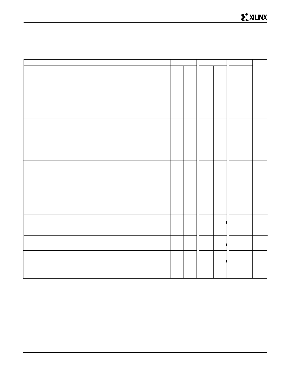
Device
XC4003E
XC4005E
XC4006E
XC4008E
XC4010E
XC4013E
XC4020E XC4025E
Appr. Gate Count
3,000
5,000
6,000
8,000
10,000
13,000
20,000
25,000
CLB Matrix
10 x 10
14 x 14
16 x 16
18 x 18
20 x 20
24 x 24
28 x 28
32 x 32
Number of CLBs
100
196
256
324
400
576
784
1,024
Number of Flip-Flops
360
616
768
936
1,120
1,536
2,016
2,560
Max Decode Inputs (per side)
30
42
48
54
60
72
84
96
Max RAM Bits
3,200
6,272
8,192
10,368
12,800
18,432
25,088
32,768
Number of IOBs
80
112
128
144
160
192
224
256
Table 1. The XC4000E Family of Field-Programmable Gate Arrays
Description
The XC4000E family of Field-Programmable Gate Arrays
(FPGAs) provides the benefits of custom CMOS VLSI,
while avoiding the initial cost, time delay, and inherent risk
of a conventional masked gate array.
The XC4000E family provides a regular, flexible, pro-
grammable architecture of Configurable Logic Blocks
(CLBs), interconnected by a powerful hierarchy of versa-
tile routing resources, and surrounded by a perimeter of
programmable Input/Output Blocks (IOBs).
XC4000E devices have generous routing resources to
accommodate the most complex interconnect patterns.
They are customized by loading configuration data into
the internal memory cells. The FPGA can either actively
read its configuration data out of external serial or byte-
parallel PROM (master modes), or the configuration data
can be written into the FPGA (slave and peripheral
modes).
The XC4000E family is supported by powerful and sophis-
ticated software, covering every aspect of design: from
schematic entry, to simulation, to automatic block place-
ment and routing of interconnects, and finally the creation
of the configuration bit stream.
FPGAs are ideal for shortening the design and develop-
ment cycle, but they also offer a cost-effective solution for
production rates well beyond 1,000 systems per month.
The XC4000E family is a superset of the popular XC4000
family. For a detailed description of the device architec-
ture, configuration methods, pin functionality, package
pin-outs and dimensions, see the Xilinx Programmable
Logic Data Book.
The following pages describes the new features of the
XC4000E family and list electrical and timing parameters.
Features
∑ Third Generation Field-Programmable Gate Arrays
≠ On-chip ultra-fast RAM with synchronous write option
≠ Dual-port RAM option
≠ Fully PCI compliant
≠ Abundant flip-flops
≠ Flexible function generators
≠ Dedicated high-speed carry-propagation circuit
≠ Wide edge decoders (four per edge)
≠ Hierarchy of interconnect lines
≠ Internal 3-state bus capability
≠ 8 global low-skew clock or signal distribution network
∑ Flexible Array Architecture
≠ Programmable logic blocks and I/O blocks
≠ Programmable interconnects and wide decoders
∑ Sub-micron CMOS Process
≠ High-speed logic and Interconnect
≠ Low power consumption
∑ Systems-Oriented Features
≠ IEEE 1149.1-compatible boundary-scan logic support
≠ Programmable output slew rate (2 modes)
≠ Programmable input pull-up or pull-down resistors
≠ 12-mA sink current per output
≠ 24-mA sink current per output pair
∑ Configured by Loading Binary File
≠ Unlimited reprogrammability
≠ Six programming modes
∑ XACT Development System runs on '386/'486/
Pentium-type PC, Apollo, Sun-4, and Hewlett-Packard
700 series
≠ Interfaces to popular design environments like
Viewlogic, Mentor Graphics and OrCAD
≠ Fully automatic partitioning, placement and routing
≠ Interactive design editor for design optimization
≠ 288 macros, 34 hard macros, RAM/ROM compiler

2
XC4000E Logic Cell Array Family
IOB Clock Enable
The two flip-flops in each IOB have a common clock enable
input,which through configuration can be activated indi-
vidually for the input or output flip-flop or both. This clock
enable operates exactly like the EC pin on the XC4000
CLB. This makes the IOBs more versatile, and avoids the
need for clock gating.
Output Drivers
The output pull-up structure can be globally configured to
be either a TTL-like totem-pole (n-channel pull-up transis-
tor, pulling to a voltage one threshold below Vcc, just like
XC4000) or to be CMOS (p-channel pull-up transistor
pulling to Vcc). Also, the configurable pull-up resistor in
XC4000E is a p-channel transistor that pulls to Vcc,
whereas in XC4000 it is an n-channel transistor that pulls
to a voltage one threshold below Vcc.
Input Thresholds
The input thresholds can be globally configured for either
TTL ( 1.2 V threshold) or CMOS ( 2.5 V threshold ), just like
XC2000 and XC3000 inputs. Note that the two global
adjustments of input threshold and output level are inde-
pendent of each other.
Global Signal Access to Logic
There is additional access from global clocks to the F and
G function generator inputs.
Mode-Pin Pull-Up Resistors
During configuration, the three mode pins, M0, M1, and
M2, have weak pull-up resistors. For the most popular
configuration mode, Slave Serial, the mode pins can thus
be left unconnected.
For user mode, the three mode inputs can individually be
configured with or without weak pull-up or pull-down
resistors
The PROGRAM input pin has a permanent weak pull-up.
Soft Startup
Like XC3000A, the XC4000E family has "Soft Startup".
When the configuration process is finished and the device
starts up in user mode, the first activation of the outputs is
automatically slew-rate limited. This avoids the potential
ground bounce when all outputs are turned on simulta-
neously. After start-up, the slew rate of the individual
outputs is, as in the XC4000 family, determined by the
individual configuration option.
XC4000E compared to XC4000
Any XC4000E device is a 100% compatible superset of the
equivalent XC4000 device, not only functionally, but also
electrically, and in pin-out and configuration bitstream.
The XC4000E devices have the following additional func-
tions, most of which are invoked through options in the
configuration bitstream:
Synchronous RAM
The two RAMs in any CLB can be changed to synchronous
write operation. In this synchronous mode, the internal
write operation is controlled by the same clock that drives
the flip-flops. The clock polarity is programmable for the
RAM (both F and G function generators together), but is
independent of the chosen flip-flop polarity. Address,
Data, and WE inputs are latched by this rising or falling
clock edge, and a short internal write pulse is generated
right after the clock edge. This self-timed write operation is
thus effectively edge-triggered.
The read operation is not affected by this change to a
synchronous write.
Dual-Port RAM
A separate option converts the 16 x 2 RAM in any CLB into
a 16 x 1 dual-port RAM. In this mode, any operation that
writes into the F-RAM, automatically also writes into the G-
RAM, using the F address. The G-address can, therefore,
not be used to write into the G-RAM.
The CLB can thus be used as an asymmetrical dual-port
RAM, with F being the read address for the F-RAM and the
write address for both F- and G-RAM, while G is the read
address for the G-RAM. Note that F and G can still be
independent read addresses, as they are in XC4000. The
two RAMs together have one read/write port using the F
address, and one read-only port using the G address.
Each CLB can be configured as function generators either
asynchronous single-port, synchronous single-port, or
synchronous dual-port.
H-Function Generator
In XC4000E, the H function generator is more versatile. Its
inputs can come not only from the F and G function
generators but also from up to three control input lines.
The H function generator can be totally or partially inde-
pendent of the other two function generators.
3
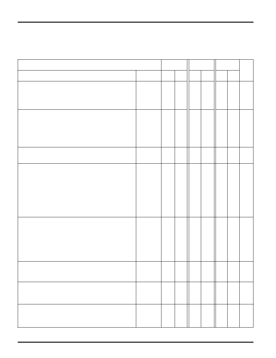
ADVANCE INFORMATION
Speed Grade
-4
-3
-2
Description
Symbol
Min
Max
Min Max
Min Max Units
Input
Propagation Delays
Pad to I1, I2
T
PID
2.5
ns
Pad to I1, I2, via transparent latch (no delay)
T
PLI
3.6
ns
Pad to I1, I2, via transparent latch (with delay)
T
PDLI
7.1
ns
Clock (IK) toI1, I2, (flip-flop)
T
IKRI
2.8
ns
Clock (IK) to I1, I2 (latch enable, active Low)
T
IKLI
3.0
ns
Set-up Time (Note 3)
Pad to Clock (IK), no delay
T
PICK
4.7
ns
Pad to Clock (IK) with delay
T
PICKD
8.3
ns
Hold Time (Note 3)
Pad to Clock (IK), no delay
T
IKPI
0
ns
Pad to Clock (IK) with delay
T
IKPID
0
ns
Output
Propagation Delays
Clock (OK) to Pad
(fast)
T
OKPOF
4.6
ns
same
(slew rate limited)
T
OKPOS
11.2
ns
Output (O) to Pad
(fast)
T
OPF
5.8
ns
same
(slew-rate limited)
T
OPS
12.4
ns
3-state to Pad begin hi-Z (slew-rate independent)
T
TSHZ
4.2
ns
3-state to Pad active and valid (fast)
T
TSONF
8.1
ns
same
(slew -rate limited)
T
TSONS
14.7
ns
Set-up and Hold Times
Output (O) to clock (OK) set-up time
T
OOK
3.7
ns
Output (O) to clock (OK) hold time
T
OKO
0
ns
Clock
Clock High or Low time
T
CH/
T
CL
4.0
ns
Global Set/Reset
Delay from GSR net through Q to I1, I2
T
RRI
7.2
ns
Delay from GSR net to Pad
T
RPO
ns
GSR width
*
T
MRW
18.9
ns
IOB Switching Characteristic Guidelines
Testing of the switching parameters is modeled after testing methods specified by MIL-M-38510/605. All devices are 100%
functionally tested. Since many internal timing parameters cannot be measured directly, they are derived from benchmark timing
patterns. The following guidelines reflect worst-case values over the recommended operating conditions. For more detailed, more
precise, and more up-to-date timing information, use the values provided by the XACT timing calculator and used in the simulator.
* Timing is based on the XC4005E. For other devices see XACT timing calculator.
** See preceding page
Notes: 1. Timing is measured at pin threshold, with 50 pF external capacitive loads (incl. test fixture). Slew rate limited output
rise/fall times are approximately two times longer than fast output rise/fall times. For the effect of capacitive loads on
ground bounce, see pages 8-8 through 8-10.
2. Voltage levels of unused (bonded and unbonded) pads must be valid logic levels. Each can be configured with the
internal pull-up or pull-down resistor or alternatively configured as a driven output or be driven from an external source.
3. Input pad setup times and hold times are specified with respect to the internal clock (IK). To calculate system setup time,
subtract clock delay (clock pad to IK) from the specified input pad setup time value, but do not subtract below zero.
Negative hold time means that the delay in the input data is adequate for the external system hold time to be zero,
provided the input clock uses the Global signal distribution from pad to IK.
4
XC4000E Logic Cell Array Family
ADVANCE INFORMATION
Speed Grade
-4
-3
-2
Description
Symbol
Min
Max
Min Max
Min Max Units
Combinatorial Delays
F/G inputs to X/Y outputs
T
ILO
2.0
ns
F/G inputs via H' to X/Y outputs
T
IHO
3.6
ns
C inputs via H' to X/Y outputs
T
HHO
2.9
ns
CLB Fast Carry Logic
Operand inputs (F1,F2,G1,G4) to C
OUT
T
OPCY
2.6
ns
Add/Subtract input (F3) to C
OUT
T
ASCY
4.4
ns
Initialization inputs (F1,F3) to C
OUT
T
INCY
1.7
ns
C
IN
through function generators to X/Y outputs
T
SUM
3.3
ns
C
IN
to C
OUT
, bypass function generators.
T
BYP
0.7
ns
Sequential Delays
Clock K to outputs Q
T
CKO
2.4
ns
Set-up Time before Clock K
F/G inputs
T
ICK
2.3
ns
F/G inputs via H'
T
IHCK
4.0
ns
C inputs via H1
T
HHCK
3.3
ns
C inputs via DIN
T
DICK
1.9
ns
C inputs via EC
T
ECCK
2.6
ns
C inputs via S/R, going Low (inactive)
T
RCK
1.7
ns
C
IN
input via F'/G'
T
CCK
ns
C
IN
input via F'/G' and H'
T
CHCK
ns
Hold Time after Clock K
F/G inputs
T
CKI
0
ns
F/G inputs via H'
T
CKIH
0
ns
C inputs via H1
T
CKHH
0
ns
C inputs via DIN
T
CKDI
0
ns
C inputs via EC
T
CKEC
0
ns
C inputs via S/R, going Low (inactive)
T
CKR
0
ns
Clock
Clock High time
T
CH
4.0
ns
Clock Low time
T
CL
4.0
ns
Set/Reset Direct
Width (High)
T
RPW
4.0
ns
Delay from C inputs via S/R, going High to Q
T
RIO
4.0
ns
Master Set/Reset*
Width (High or Low)
T
MRW
18.9
ns
Delay from Global Set/Reset net to Q
T
MRQ
14.4
ns
CLB Switching Characteristic Guidelines
Testing of the switching parameters is modeled after testing methods specified by MIL-M-38510/605. All devices are 100%
functionally tested. Since many internal timing parameters cannot be measured directly, they are derived from benchmark timing
patterns. The following guidelines reflect worst-case values over the recommended operating conditions. For more detailed, more
precise, and more up-to-date timing information, use the values provided by the XACT timing calculator and used in the simulator.
*
Timing is based on the XC4005E. For other devices see XACT timing calculator.