DS015 (v1.3) October 18, 1999 - Product Specification
6-157
6
XC4000XLA/XV Family Features
Note: XC4000XLA devices are improved versions of
XC4000XL devices. The XC4000XV devices have the
same features as XLA devices, incorporate additional inter-
connect resources and extend gate capacity to 500,000
system gates. The XC4000XV devices require a separate
2.5V power supply for internal logic but maintain 5V I/O
compatibility via a separate 3.3V I/O power supply. For
additional information about the XC4000XLA/XV device
architecture, refer to the XC4000E/X FPGA Series general
and functional descriptions.
∑
System-featured Field-Programmable Gate Arrays
-
Select-RAM
TM
memory: on-chip ultra-fast RAM with
-
Synchronous write option
-
Dual-port RAM option
-
Flexible function generators and abundant flip-flops
-
Dedicated high-speed carry logic
-
Internal 3-state bus capability
-
Eight global low-skew clock or signal distribution
networks
∑
Flexible Array Architecture
∑
Low-power Segmented Routing Architecture
∑
Systems-oriented Features
-
IEEE 1149.1-compatible boundary scan
-
Individually programmable output slew rate
-
Programmable input pull-up or pull-down resistors
-
Unlimited reprogrammability
∑
Read Back Capability
-
Program verification and internal node observability
Electrical Features
∑
XLA Devices Require 3.0 - 3.6 V (VCC)
∑
XV Devices Require 2.3- 2.7 V (VCCINT)
and 3.0 - 3.6 V (VCCIO)
∑
5.0 V TTL compatible I/O
∑
3.3 V LVTTL, LVCMOS compliant I/O
∑
5.0 V and 3.0 V PCI Compliant I/O
∑
12 mA or 24 mA Current Sink Capability
∑
Safe under All Power-up Sequences
∑
XLA Consumes 40% Less Power than XL
∑
XV Consumes 65% Less Power than XL
∑
Optional Input Clamping to VCC (XLA) or VCCIO (XV)
Additional Features
∑
Footprint Compatible with XC4000XL FPGAs - Lower
cost with improved performance and lower power
∑
Advanced Technology -- 5 layer metal, 0.25
µ
m CMOS
process (XV) or 0.35
µ
m CMOS process (XLA)
∑
Highest Performance -- System erformance beyond
100 MHz
∑
High Capacity -- Up to 500,000 system gates and
270,000 synchronous SRAM bits
∑
Low Power -- 3.3 V/2.5 V technology plus segmented
routing architecture
∑
Safe and Easy to Use -- Interfaces to any combination
of 3.3 V and 5.0 V TTL compatible devices
0
XC4000XLA/XV Field Programmable
Gate Arrays
DS015 (v1.3) October 18, 1999
0
0*
Product Specification
R
*
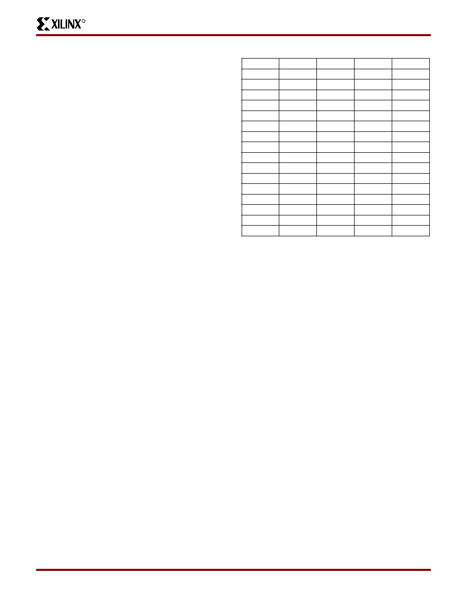
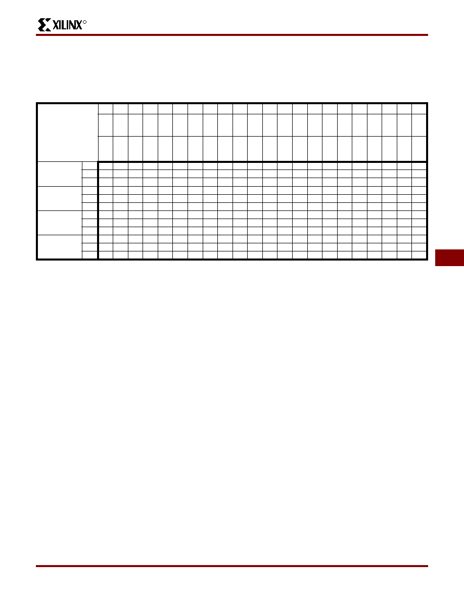
Table 1: XC4000XLA Series Field Programmable Gate Arrays
Device
Logic
Cells
Max Logic
Gates
(No RAM)
Max. RAM
Bits
(No Logic)
Typical
Gate Range
(Logic and RAM)*
CLB
Matrix
Total
CLBs
Number
of
Flip-Flops
Max.
User I/O
Required
Configur-
ation Bits
XC4013XLA
1,368
13,000
18,432
10,000 - 30,000
24 x 24
576
1,536
192
393,632
XC4020XLA
1,862
20,000
25,088
13,000 - 40,000
28 x 28
784
2,016
224
521,880
XC4028XLA
2,432
28,000
32,768
18,000 - 50,000
32 x 32
1,024
2,560
256
668,184
XC4036XLA
3,078
36,000
41,472
22,000 - 65,000
36 x 36
1,296
3,168
288
832,528
XC4044XLA
3,800
44,000
51,200
27,000 - 80,000
40 x 40
1,600
3,840
320
1,014,928
XC4052XLA
4,598
52,000
61,952
33,000 - 100,000
44 x 44
1,936
4,576
352
1,215,368
XC4062XLA
5,472
62,000
73,728
40,000 - 130,000
48 x 48
2,304
5,376
384
1,433,864
XC4085XLA
7,448
85,000
100,352
55,000 - 180,000
56 x 56
3,136
7,168
448
1,924,992
XC40110XV
9,728
110,000
131,072
75,000 - 235,000
64 x 64
4,096
9,216
448
2,686,136
XC40150XV
12,312
150,000
165,888
100,000 - 300,000
72 x 72
5,184
11,520
448
3,373,448
XC40200XV
16,758
200,000
225,792
130,000 - 400,000
84 x 84
7,056
15,456
448
4,551,056
XC40250XV
20,102
250,000
270,848
180,000 - 500,000
92 x 92
8,464
18,400
448
5,433,888
*
Maximum values of gate range assume 20-30% of CLBs used as RAM

R
XC4000XLA/XV Field Programmable Gate Arrays
6-158
DS015 (v1.3) October 18, 1999 - Product Specification
General Description
XC4000 Series high-performance, high-capacity Field Pro-
grammable Gate Arrays (FPGAs) provide the benefits of
custom CMOS VLSI, while avoiding the initial cost, long
development cycle, and inherent risk of a conventional
masked gate array.
The result of fifteen years of FPGA design experience and
feedback from thousands of customers, these FPGAs com-
bine architectural versatility, increased speed, abundant
routing resources, and new, sophisticated software to
achieve fully automated implementation of complex,
high-density, high-performance designs.
Technology Advantage
XC4000XLA/XV FPGAs use 5 layer metal silicon technol-
ogy to improve performance while reducing device cost and
power. In addition, IOB enhancements provide full PCI
compliance and the JTAG functionality is expanded.
Low Power Internal Logic
XC4000XV FPGAs incorporate all the features of the XLA
devices but require a separate 2.5V power supply for inter-
nal logic. I/O pads are still driven from a 3.3V power supply.
The 2.5V logic supply is named VCCINT and the 3.3 V IO
supply is named VCCIO.
The XV devices also incorporate additional routing
resources in the form of 8 octal-length segmented routing
channels vertically and horizontally per row and column.
XLA/XV and XL Family Differences
The XC4000XLA/XV families of FPGAs are logically identi-
cal to XC4000EX and XC4000XL FPGAs, however I/O,
configuration logic, JTAG functionality, and performance
have been enhanced. In addition, they deliver:
∑
Improved Performance
XLA/XV devices benefit from advance processing
technology and a reduction in interconnect capacitance
which improves performance over XL devices by more
than 30%.
∑
Lower Power
XLA/XV devices have reduced power requirements
compared to equivalent XL devices.
∑
Shorter routing delays
The smaller die of XLA/XV devices directly reduces
clock delays and the delay of high-fanout signals. The
reduction in clock delay allows improved pin-to-pin I/O
specifications.
∑
Lower Cost
XLA/XV device cost is directly related to the die size
and has been reduced significantly from that of
equivalent XL devices.
∑
Express mode configuration
Express mode configuration is available on the XLA and
XV devices.
IOB Enhancements
∑
12/24 mA Output Drive
The XLA/XV family of FPGAs allow individual IOBs to
be configured as high drive outputs. Each output can be
configured to have 24 mA drive strength as opposed to
the standard default strength of 12 mA.
∑
VCC Clamping Diode
XLA and XV FPGAs have an optional clamping diode
connected from each output to VCC (VCCIO for XV).
When enabled they clamp ringing transients back to the
3.3V supply rail. This clamping action is required in
3.3V PCI applications. VCC clamping is a global option
affecting all I/O pins. If enabled, TTL I/O compatibility is
maintained, but full 5.0 Volt I/O tolerance is sacrificed.
∑
Enhanced ESD protection
An improved ESD structure allows XV devices to safely
pass the stringent 5V PCI (4.2.1.3) ringing test. This
test applies an 11V pulse to each IOB for 11 ns via a 55
ohm resistor.
∑
Full 3.3V and 5.0V PCI compliance
The addition of 12/24 mA drive, optional 3.3V clamping
and improved ESD provides full compliance with either
3.3V or 5.0V PCI specifications.
Figure 1: Cross Section of Xilinx 0.25 micron, 5 layer
metal XC4000XV FPGA. Visible features are five layers of
metallization, tungsten plug vias and trench isolation. The
small gaps above the lowest layer are 0.25 micron
polysilicon MOSFET gates. The excellent planarity of each
metal layer is due to the use of "chemical-mechanical
polishing" or CMP. In effect, each layer is ground flat before
a new layer is added.
R
DS015 (v1.3) October 18, 1999 - Product Specification
6-159
XC4000XLA/XV Field Programmable Gate Arrays
6
Three-State Register
XC4000XLA/XV devices incorporate an optional register
controlling the three-state enable in the IOBs.The use of
the three-state control register can significantly improve
output enable and disable time.
FastCLK Clock Buffers
The XLA/XV devices incorporate FastCLK clock buffers.
Two FastCLK buffers are available on each of the right and
left edges of the die. Each FastCLK buffer can provide a
fast clock signal (typically < 1.5 ns clock delay) to all the
IOBs within the IOB octant containing the buffer. The Fast-
CLK buffers can be instantiated by use of the BUFFCLK
symbols. (In addition to FastCLK buffers, the Global Early
BUFGE clock buffers #1, #2, #5, and #6 can also provide
fast clock signals (typically < 1.5 ns clock delay) to IOBs on
the top and bottom of the die.
XLA/XV Power Requirements
XC4000XLA devices require 40% less power per CLB than
equivalent XL devices. XC4000XV devices require 42%
less power per CLB than equivalent XLA devices and 65%
less power than XL devices The representative K-Factor for
the following families can be found in
Table 2
. The K-Factor
predicts device current for typical user designs and is
based on filling the FPGA with active 16-Bit counters and
measuring the device current at 1 MHz. This technique is
described in XBRF14 "A Simple Method of Estimating
Power in XC4000XL/EX/E FPGAs". To predict device
power (P) using the K-Factor use the following formula:
P=V*K*N*F; where:
P= Device Power
V= Power supply voltage
K= the Device K-Factor
N = number of active registers
F = Frequency in MHz
XLA/XV Logic Performance
XC4000XLA/XV devices feature 30% faster device speed
than XL devices, and consistent performance is achieved
across all family members.
Table 3
illustrates the perfor-
mance of the XLA devices. For details regarding the imple-
mentation of these benchmarks refer to XBRF15 "Speed
Metrics for High Performance FPGAs".
Table 2: K-Factor and Relative Power.
FPGA Family
K-Factor
Power
Relative To
XL
Power
Relative To
XLA
XC4000XL
28
1.00
1.65
XC4000XLA
17
0.60
1.00
XC4000XV
13
0.35
0.58
Table 3: XLA/XV Estimated Benchmark Performance
Register - Register
Benchmarks
Size
Maximum
Frequency
Adder
8-Bit
172 MHz
16-Bit
144 MHz
32-Bit
108 MHz
2 Cascaded Adders
16-Bit
94 MHz
4 Cascaded Adders
16-Bit
57 MHz
Cascaded 4LUTs
1 Level
314 MHz
2 Level
193 MHz
4 Level
108 MHz
6 Level
75 MHz
Interconnect
(Manhattan Distance)
1 CLBs
325 MHz
4 CLBs
260 MHz
16 CLBs
185 MHz
64 CLBs
108 MHz
128 CLBs
81 MHz
Dual Port RAM
(Pipelined)
8-Bits by 16
172 MHz
8-Bits by 256
172 MHz
R
XC4000XLA/XV Field Programmable Gate Arrays
6-160
DS015 (v1.3) October 18, 1999 - Product Specification
Using Fast I/O CLKS
There are several issues associated with implementing fast
I/O clocks by using multiple FastCLK and BUFGE clock
buffers for I/O transfers and a BUFGLS clock buffer for
internal logic.
Reduced Clock to Out Period - When transferring data
from a BUFGLS clocked register to an IOB output register
which is clocked with a fast I/O clock, the total amount of
time available for the transfer is reduced.
Using Fast Capture Latch in IOB input - It is necessary to
transfer data captured with the fast I/O clock edge to a
delayed BUFGLS clock without error. The use of the Fast
Capture Latch in the IOBs provides this functionality.
Driving multiple clock inputs - Since each FastCLK input
can only reach one octant of IOBs it will usually be neces-
sary to drive multiple FastCLK and BUFGE input pads with
a copy of the system clock. Xilinx recommends that sys-
tems which use multiple FastCLK and BUFGE input buffers
use a "Zero Delay" clock buffer such as the Cypress
CY2308 to drive up to 8 input pins. These devices contain a
Phase locked loop to eliminate clock delay, and specify less
than 250ps output jitter.
PCB layout - The recommended layout is to place the PLL
underneath the FPGA on the reverse side of the PCB. All 8
clock lines should be of equal length. This arrangement will
allow all the clock line to be less than 2 cm in length which
will generally eliminate the need for clock termination.
Advancing the FPGAs clock - An additional advantage to
using a PLL-equipped clock buffer is that it can advance the
FPGA clocks relative to the system clock by incorporating
additional board delay in the feedback path. Approximately
6 inches of trace length are necessary to delay the signal
by 1 ns.
Advancing the FPGA's clock directly reduces input hold
requirements and improves clock to out delay. FPGA clocks
should not be advanced more than the guaranteed mini-
mum Output Hold Time (minus any associated clock jitter)
or the outputs may change state before the system clock
edge. For XLA and XV FPGAs the Output Hold Time is
specified as a minimum Clock to Output Delay in the tables
in the respective family Electrical Specification sections.
The maximum recommended clock advance equals this
value minus any clock jitter.
Instantiating I/O elements- Depending on the design
environment, it may be necessary to instantiate the fast I/O
elements. They are found in the libraries as:
∑
BUFGE (I,O) - The Global Early Buffer
∑
BUFGLS (I,O)- The Global Low Skew Buffer
∑
BUFFCLK (I,O) - The FastCLK Buffer
∑
ILFFX (D, GF, CE, C, Q) - The Fast Capture Latch
Macro
Locating I/O elements - It is necessary to connect these
elements to a particular I/O pad in order to select which
buffer or fast capture latch will be used.
Restricted Clock Loading - Because the input hold
requirement is a function of internal clock delay, it may be
necessary to restrict the routing of BUFGE to IOBs along
the top and bottom of the die to obtain sub-ns clock delays.
BUFGE 1
BUFGE 2
FCLK 3
FCLK 4
BUFGE 5
FCLK 2
FCLK 1
BUFGE 6
BUFGLS 2
Figure 2: Location of FastCLK, BUFGE and BUFGLS
Clock Buffers in XC4000XLA/XV FPGAs
BUFGE
1
BUFGE
2
BUFGE
5
BUFGE
6
FCLK1
FCLK2
FCLK3
FCLK4
PLL
Clock
Buffer
O0
O1
O2
O3
O4
O5
O6
O7
FB
Ref
XC4000XLA
XC4000XV
SysClk
Figure 3: Diagram of XC4000XLA/XV FPGA
Connected to PLL Clock Buffer Driving 4 BUFGE and
4 FastCLK Clock Buffers.
R
DS015 (v1.3) October 18, 1999 - Product Specification
6-161
XC4000XLA/XV Field Programmable Gate Arrays
6
JTAG Enhancements
XC4000XLA/XV devices have improved JTAG functionality
and performance in the following areas:
∑
IDCODE - The IDCODE register in JTAG is now
supported. All future Xilinx FPGAs will support the
IDCODE register. By using the IDCODE, the device
connected to the JTAG port can be determined. The
use of the IDCODE enables selective configuration
dependent upon the FPGA found. The IDCODE register
has the following binary format:
vvvv:ffff:fffa:aaaa:aaaa:cccc:cccc:ccc1
Where:
c = the company code;
a = the array dimension in CLBs;
f = the Family code;
v = the die version number
Xilinx company code = 49 (hex)
∑
Configuration State - The configuration state is
available to JTAG controllers.
∑
Configure Disable - The JTAG port can be prevented
from reconfiguring the FPGA
∑
TCK Startup - TCK can now be used to clock the
start-up block in addition to other user clocks.
∑
CCLK holdoff - Changed the requirement for Boundary
Scan Configure or EXTEST to be issued prior to the
release of INIT pin and CCLK cycling.
∑
Reissue configure - The Boundary Scan Configure
can be reissued to recover from an unfinished attempt
to configure the device.
∑
Bypass FF - Bypass FF and IOB is modified to provide
DRCLOCK only during BYPASS for the bypass flip-flop
and during EXTEST or SAMPLE/PRELOAD for the IOB
register.
XV and XLA Family Differences
The high density of the XC4000XV family FPGAs is
achieved by using advanced 0.25 micron silicon technol-
ogy. A 2.5 Volt power supply (VCCINT) is necessary to pro-
vide the reduced supply voltage required by 0.25 micron
internal logic, however to maintain TTL compatibility a 3.3V
power supply (VCCIO) is required by the I/O.
To accommodate the higher gate capacity of XV devices,
additional interconnect has been added. These differences
are detailed below.
∑
VCCINT (2.5 Volt) Power Supply Pins
The XV family of FPGAs requires a 2.5V power supply
for internal logic, which is named VCCINT. The pins
assigned to the VCCINT supply are named in the pinout
guide for the XC4000XV FPGAs and in
Table 5 on page
162
.
∑
VCCIO (3.3 Volt) Power Supply Pins
Both the XV and XLA FPGAs use a 3.3V power supply
to power the I/O pins. The I/O supply is named VCCIO
in the XV family.
∑
Octal-Length Interconnect Channels
The XC40110XV, XC40150XV, XC40200XV, and
XC40250XV have enhanced routing. Eight routing
channels of octal length have been added to each CLB
in both vertical and horizontal dimensions.
XLA-to-XL Socket Compatibility
The XC4000XLA devices are generally available in the
same packages as equivalent XL devices, however the
range of packages available for the XC4085XLA has been
extended to include smaller packages such as the HQ240.
XV-to-XL/XLA Socket Compatibility
XC4000XV devices are available in five package options,
pin-grid PG599 and ball-grid BG560, BG432, and BG352
and quad-flatpack HQ240. With the exception of the
VCCINT power pins, XC4000XV FPGAs are compatible
with XL and XLA devices in these packages if the following
guidelines are followed:
∑
Lay out the PCB for the XV pinout.
∑
When an XL or XLA device is installed disconnect the
VCCINT (2.5 V) supply. For the PG599, VCCINT should
be connected to 3.3V. For BG560, BG432 and BG352
and HQ240 packages, the VCCINT voltage source
should be left unconnected. The unused I/O pins in the
XL/XLA devices connected to VCCINT will be pulled up
to 3.3V. Care must be taken to insure that these pins
are not driven when the XL/XLA device is operative.
∑
When an XC4000XV is installed, the VCCINT pins must
Family Codes = 01 for XLA;
= 02 for SpartanXL;
= 03 for Virtex;
= 07 for XV.
Table 4: IDCODEs assigned to XC4000XLA/XV FPGAs
FPGA
IDCODE
XC4013XLA
0x00218093
XC4020XLA
0x0021c093
XC4028XLA
0x00220093
XC4036XLA
0x00224093
XC4044XLA
0x00228093
XC4052XLA
0x0022c093
XC4062XLA
0x00230093
XC4085XLA
0x00238093
XC40110XV
0x00e40093
XC40150XV
0x00e48093
XC40200XV
0x00e54093
XC40250XV
0x00e5c093
R
XC4000XLA/XV Field Programmable Gate Arrays
6-162
DS015 (v1.3) October 18, 1999 - Product Specification
be connected to a 2.5V power supply.
The differences between the XL and XV packages are
detailed below:
PG559 - XLA and XL devices in the PG599 package have
56 VCC pins.The XC4000XV devices allocate 16 of these
I/O pins to VCCINT (2.5V).
BG560 - XLA and XL devices in the BG560 package have
448 I/O pins.The XC4000XV devices allocate 16 of these
I/O pins to VCCINT (2.5V).
BG432- XLA and XL devices in the BG432 package have
352 I/O pins. The XC4000XV devices allocate 16 of these
I/O pins to VCCINT (2.5V).
BG352 - XLA and XL devices in the BG352 package have
289 I/O pins.The XC4000XV devices allocate 15 of these
I/O pins to VCCINT (2.5V).
HQ240- XLA and XL devices in the HQ240 package have
193 I/O pins.The XC4000XV devices allocate 15 of these
I/O pins to VCCINT (2.5V).
Table 5: VCCINT (2.5 V) Pins in XV Packages
HQ240
BG352
BG432
BG560
PG559
P198
D10
A10
E12
H12
P185
D5
AB2
AD2
H18
P164
K4
AB30
AD32
H26
P154
N3
AG28
AK31
H32
P137
W2
AH15
AM17
M8
P116
AE3
AH5
AK5
M36
P104
AC10
AJ10
AK11
V8
P93
AC13
AK22
AN25
V36
P77
AE19
B23
C24
AF8
P55
AB24
B4
D6
AF36
P43
V24
C16
C17
AM8
P27
N24
E28
E30
AM36
P16
J24
K29
K32
AT12
P4
D24
K3
J1
AT18
P225
A20
R2
T3
AT26
-
-
R29
U32
AT32

R
DS015 (v1.3) October 18, 1999 - Product Specification
6-163
XC4000XLA/XV Field Programmable Gate Arrays
6
I/O Signalling Standards
XLA and XV devices are compatible with TTL, LVTTL, PCI
3V, PCI 5V and LVCMOS signalling. The various standards
are illustrated in
Table 6
and the signaling environment is
illustrated in
Figure 4
.
VCC Clamping
XLA/XV devices are fully 5V TTL I/O compatible if VCC
clamping is not enabled. The I/O pins can withstand input
voltages up to 7V. With VCC clamping enabled, the XLA/XV
devices will begin to clamp input voltages to one diode volt-
age drop above VCC. In both cases negative voltage is
clamped to one diode voltage drop below ground.
XLA/XV devices maintain LVTTL I/O compatibility when
VCC clamping is enabled, however full 5.0V TTL I/O com-
patibility is sacrificed.
Overshoot and Undershoot
Ringing wave forms are allowed on XLA/XV inputs as long
as undershoot is limited to -2.0V and overshoot is limited to
+7.0V and current is limited to 100 mA for less than 10 ns.
If VCC clamping is enabled then overshoot will begin to be
clamped at VCC/VCCIO plus one diode voltage drop and
undershoot will be clamped to ground minus one diode volt-
age drop. In either case the current must be limited to 100
mA per pin for less than 10 ns.
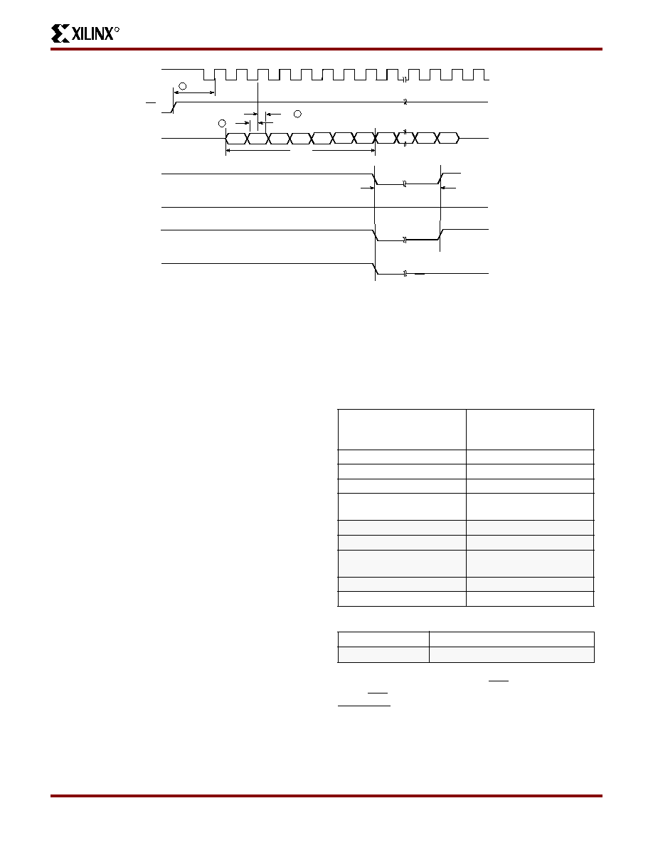
Express Configuration Mode
Express configuration mode is similar to Slave Serial con-
figuration mode, except that data is processed one byte per
CCLK cycle instead of one bit per CCLK cycle. An external
source is used to drive CCLK, while byte-wide data is
loaded directly into the configuration data shift registers
(
Figure 5
). A CCLK frequency of 10 MHz is equivalent to a
80 MHz serial rate, because eight bits of configuration data
are loaded per CCLK cycle. Express mode does not sup-
port CRC error checking, but does support constant-field
error checking. A length count is not used in Express mode.
Express mode must be specified as an option to the BitGen
program, which generates the bitstream. The Express
mode bitstream is not compatible with the other configura-
tion modes. Express mode is selected by a <010> on the
mode pins (M2, M1, M0).
The first byte of parallel configuration data must be avail-
able at the D inputs of the FPGA a short setup time before
the second rising CCLK edge. Subsequent data bytes are
Table 6: I/O Standards supported by XC4000XLA and XV FPGAs
Signaling
Standard
VCC
Clamping
Output Drive
V
IH_MAX
V
IH MIN
V
IL MAX
V
OH MIN
V
OL MAX
TTL
Not allowed
12/24 mA
5.5
2.0
0.8
2.4
0.4
LVTTL
OK
12/24 mA
3.6
2.0
0.8
2.4
0.4
PCI5V
Not allowed
24 mA
5.5
2.0
0.8
2.4
0.4
PCI3V
Required
12 mA
3.6
50% of
VCC/VCCIO
30% of
VCC/VCCIO
90% of
VCC/VCCIO
10% of
VCC/VCCIO
LVCMOS 3V
OK
12/24 mA
3.6
50% of
VCC/VCCIO
30% of
VCC/VCCIO
90% of
VCC/VCCIO
10% of
VCC/VCCIO
V
CC
(5 V)
5.0 V Power
3.3 V Power
2.5 V Power
Ground
TTL
LVTTL
5 Volt Device
V
CCIO
V
CCINT
LVTTL
XC4000XV
V
CC
(3.3 V)
3.3 Volt Device
X7147
Figure 4: The Signalling Environment for XLA/XV FPGAS. For XLA devices the VCCIO and VCCINT supplies are
replaced by a single 3.3 Volt VCC supply, however, all indicated I/O signalling is still supported.

R
XC4000XLA/XV Field Programmable Gate Arrays
6-164
DS015 (v1.3) October 18, 1999 - Product Specification
clocked in on each consecutive rising CCLK edge
(
Figure 6
).
Pseudo Daisy Chain
As illustrated in Figures 5 and 6, multiple devices with dif-
ferent configurations can be configured in a pseudo daisy
chain provided that all of the devices are in Express mode.
A single combined byte-wide data stream is used to config-
ure the chain of Express mode devices. CCLK pins are tied
together and D0-D7 pins are tied together as a data buss
for all devices along the chain. A status signal is passed
from DOUT of each device to the CS1 input of the device
which follows it in the chain. Frame data is accepted only
when CS1 is High and the device's configuration memory is
not already full. The lead device in the chain has its CS1
input tied High (or floating, since there is an internal pullup).
The status pin DOUT is initially High for all devices in the
chain until the data stream header of seven bytes is loaded.
This allows header data to be loaded into all devices in the
chain simultaneously. After the header is loaded in all
devices, their DOUT pins are pulled Low disabling configu-
ration of all devices in the chain except the first device. As
each device in the chain is filled, its DOUT goes High driv-
ing High the CS1 input of the next device, thereby enabling
configuration of the next device in the pseudo daisy chain.
The requirement that all DONE pins in a daisy chain be
wired together applies only to Express mode, and only if all
devices in the chain are to become active simultaneously.
All 4000XLA/XV devices in Express mode are synchro-
nized to the DONE pin. User I/O for each device becomes
active after the DONE pin for that device goes High (The
exact timing is determined by BitGen options.)
Since the DONE pin is open-drain and does not drive a
High value, tying the DONE pins of all devices together pre-
vents all devices in the chain from going High until the last
device in the chain has completed its configuration cycle. If
the DONE pin of a device is left unconnected, the device
becomes active as soon as that device has been config-
ured.
Because only XC4000XLA/XV, SpartanXL, and XC5200
devices support Express mode, only these devices can be
used to form an Express mode pseudo daisy chain.
Table 7: Pin Functions During Configuration
(4000XLA/XV Express mode only)
CONFIGURATION MODE
<M2:M1:M0>
USER
OPERATION
EXPRESS MODE
<0:1:0>
PIN FUNCTION
M2(LOW) (I)
M2
M1(HIGH) (I)
M1
M0(LOW) (I)
M0
HDC (HIGH)
I/O
LDC (LOW)
I/O
INIT
I/O
DONE
DONE
PROGRAM (I)
PROGRAM
CCLK (I)
CCLK (I)
DATA 7 (I)
I/O
DATA 6 (I)
I/O
DATA 5 (I)
I/O
DATA 4 (I)
I/O
DATA 3 (I)
I/O
DATA 2 (I)
I/O
DATA 1 (I)
I/O
DATA 0 (I)
I/O
DOUT
SGCK4-I/O
TDI
TDI-I/O
TCK
TCK-I/O
TMS
TMS-I/O
TDO
TDO-(O)
CS1
I/O
Notes
1. A shaded table cell represents the internal
pull-up used before and during
configuration.
2. (I) represents an input; (O) represents an
output.
3. INIT is an open-drain output during
configuration.
R
DS015 (v1.3) October 18, 1999 - Product Specification
6-165
XC4000XLA/XV Field Programmable Gate Arrays
6
Table 8: Express Mode Programming Switching Characteristic
Description
Symbol
Min
Max
Units
CCLK
INIT (High) setup time
T
IC
5
µ
s
D0 - D7 setup time
T
DC
20
ns
D0 - D7 hold time
T
CD
0
ns
CCLK High time
T
CCH
45
ns
CCLK Low time
T
CCL
45
ns
CCLK Frequency
F
CC
10
MHz
Preliminary
INIT
CCLK
CCLK
4000XLA/XV
M0
M2
CS1
D0-D7
DATA BUS
PROGRAM
INIT
CCLK
PROGRAM
INIT
DOUT
DONE
DONE
DOUT
To Additional
Optional
Daisy-Chained
Devices
To Additional
Optional
Daisy-Chained
Devices
Optional
Daisy-Chained
4000XLA/XV
M0
M2
VCC
VCC
4.7K
CS1
D0-D7
PROGRAM
99010800
8
8
8
M1
M1
Figure 5: Express Mode Circuit Diagram
R
XC4000XLA/XV Field Programmable Gate Arrays
6-166
DS015 (v1.3) October 18, 1999 - Product Specification
Data Stream Format
The data stream ("bitstream") format is identical for all
serial
configuration
modes,
but
different
for
the
4000XLA/XV Express mode. In Express mode, the device
becomes active when DONE goes High, therefore no
length count is required. Additionally, CRC error checking is
not supported in Express mode. The data stream format is
shown in
Table 9
. Express mode data is shown with D0 at
the left and D7 at the right.
The configuration data stream begins with two bytes of
eight ones each, a preamble code of one byte, followed by
three bytes of eight ones each, and finally an end-of-
header field check byte. This header of seven bytes is fol-
lowed by the actual configuration data in frames. The
length and number of frames depends on the device type.
Each frame begins with a start field and ends with an
end-of-frame field check byte. In all cases, additional
start-up bytes of data are required to provide six, or more,
clocks for the start-up sequence at the end of configuration.
Long daisy chains require additional startup bytes to shift
the last data through the chain. All startup bytes are
don't-cares; these bytes are not included in bitstreams cre-
ated by the Xilinx software.
A selection of CRC or non-CRC error checking is allowed
by the bitstream generation software. The 4000XLA
Express mode only supports non-CRC error checking. The
non-CRC
error
checking
tests
for
a
designated
end-of-frame field check byte for each frame. non-CRC
error checking tests for a designated end-of-frame field
check byte for each frame.
LEGEND:
Detection of an error results in the suspension of data load-
ing and the pulling down of the INIT pin. The user must
detect INIT and initialize a new configuration by pulsing the
PROGRAM pin Low or cycling VCC.
Note: CS1
must remain High throughout loading of the configuration data stream. In the pseudo daisy chain of
Figure 5
, the 7 byte
data stream header is loaded into all devices simultaneously. Each device's data frames are then loaded in turn when its
CS1 pin is driven High by the DOUT of the preceding device in the chain.
99012600
BYTE
0
CCLK
1
2
3
INIT
T
DC
T
CD
T
IC
D0-D7
DOUT
CS1
First
FPGA
BYTE
1
BYTE
2
BYTE
3
First FPGA Filled
BYTE
4
BYTE
5
BYTE
6
Header
Header Loaded
CS1
Second
FPGA
CS1 all
downstream
FPGAs
Byte A is first frame byte for first FPGA
Byte B is last frame byte for first FPGA
Byte C is first frame byte for second FPGA
BYTE
A
BYTE
C
BYTE
B
Figure 6: Express Mode Configuration Switching Waveforms
Table 9: 4000XLA/XV Express Mode Data Stream
Format
Data Type
Express Mode
(D0-D7)
(4000XLA only)
Fill Byte
FFFFh
Preamble Code
11110010b
Fill Byte
FFFFFFh
End-of-Header
Field Check Byte
11010010b
Start Field
11111110b
Data Frame
DATA(n-1:0)
End-of-Frame
Field Check Byte
11010010b
Extend Write Cycle
FFD2FFFFFFh
Start-Up Bytes
FFFFFFFFFFFFh
Unshaded
Once per data stream
Light
Once per data frame
R
DS015 (v1.3) October 18, 1999 - Product Specification
6-167
XC4000XLA/XV Field Programmable Gate Arrays
6
Serial PROM Recommendation
Table 10
shows the physical characteristics of each XLA/XV family member and the recommended Xilinx Serial PROM
recommended for use as configuration storage.
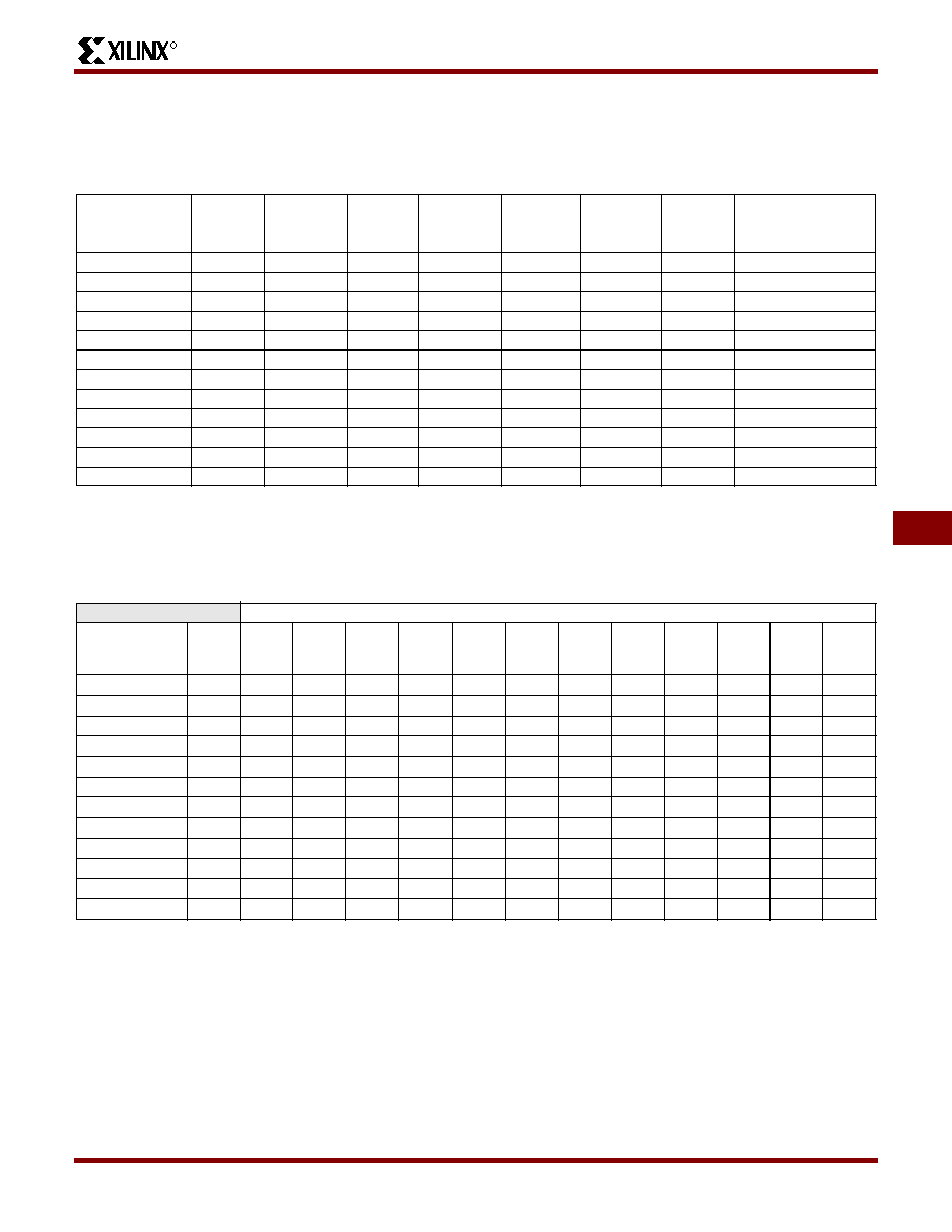
Table 10: Physical Characteristics and Recommended Serial PROM
User I/O Per Package
Table 11
shows the number of user I/Os available in each package for XC4000XLA/XV-Series devices. Call your local sales
office for the latest availability information.
Device
Max.
User I/O
CLB
Matrix
Total
CLBs
Logic
Cells
Number
of
Flip-Flops
Max. RAM
Bits
(No Logic)
Required
Configur-
ation Bits
Serial PROM
XC4013XLA
192
24 x 24
576
1,368
1,536
18,432
393,632
XC17512L
XC4020XLA
224
28 x 28
784
1,862
2,016
25,088
521,880
XC17512L
XC4028XLA
256
32 x 32
1,024
2,432
2,560
32,768
668,184
XC1701L
XC4036XLA
288
36 x 36
1,296
3,078
3,168
41,472
832,528
XC1701L
XC4044XLA
320
40 x 40
1,600
3,800
3,840
51,200
1,014,928
XC1701L
XC4052XLA
352
44 x 44
1,936
4,598
4,576
61,952
1,215,368
XC1702L
XC4062XLA
384
48 x 48
2,304
5,472
5,376
73,728
1,433,864
XC1702L
XC4085XLA
448
56 x 56
3,136
7,448
7,168
100,352
1,924,992
XC1702L
XC40110XV
448
64 x 64
4,096
9,728
9,216
131,072
2,686,136
XC1704L
XC40150XV
448
72 x 72
5,184
12,312
11,520
165,888
3,373,448
XC1704L
XC40200XV
448
84 x 84
7,056
16,758
15,456
225,792
4,551,056
XC1704L+XC17512L
XC40250XV
448
92 x 92
8,464
20,102
18,400
270,848
5,433,888
XC1704L+XC1702L
Table 11: User I/O Pins Available by Device and Package
Maximum I/O Accessible per Package
Device
Max
I/O
HQ160
PQ160
HQ208
PQ208
HQ240
PQ240
BG256
HQ304
BG352
BG432
PG559
BG560
XC4013XLA
192
129
160
192
192
XC4020XLA
224
129
160
193
205
XC4028XLA
256
129
160
193
205
256
XC4036XLA
288
129
160
193
288
288
XC4044XLA
320
129
160
193
256
289
320
XC4052XLA
352
129
160
193
256
289
352
352
XC4062XLA
384
129
160
193
256
289
352
384
XC4085XLA
448
129
160
193
256
289
352
448
XC40110XV
448
178
274
336
432
XC40150XV
448
178
274
336
448
432
XC40200XV
448
336
432
XC40250XV
448
336
448
432

R
XC4000XLA/XV Field Programmable Gate Arrays
6-168
DS015 (v1.3) October 18, 1999 - Product Specification
Product Availability
XLA Family
Table 12 shows the current available package and speed grade combinations for XC4000XLA Series devices. Call your local
sales office for the latest availability information, or see the Xilinx W
EB
LINX at http://www.xilinx.com for the latest revision of
the specifications.
Table 12: Component Availability Chart for XC4000XLA FPGAs
PINS
84
100
100
144
144
160
160
176
176
208
208
240
240
256
299
304
352
411
432
475
559
560
TYPE
Plast.
PLCC
Plast.
PQFP
Plast.
VQFP
Plast.
TQFP
High-Perf.
TQFP
High-Perf.
QFP
Plast.
PQFP
Plast.
TQFP
High-Perf.
TQFP
High-Perf.
QFP
Plast.
PQFP
High-Perf.
QFP
Plast.
PQFP
Plast.
BGA
Ceram.
PGA
High-Perf.
QFP
Plast.
BGA
Ceram.
PGA
Plast.
BGA
Ceram.
PGA
Ceram.
PGA
Plast.
BGA
CODE
PC84
PQ100
VQ100
TQ144
HT144
HQ160
PQ160
TQ176
HT176
HQ208
PQ208
HQ240
PQ240
BG256
PG299
HQ304
BG352
PG411
BG432
PG475
PG559
BG560
XC4013XLA
-09
C I
C I
C I
C I
-08
C I
C I
C I
C I
-07
C
C
C
C
XC4020XLA
-09
C I
C I
C I
C I
-08
C I
C I
C I
C I
-07
C
C
C
C
XC4028XLA
-09
C I
C I
C I
C I
C I
-08
C I
C I
C I
C I
C I
-07
C
C
C
C
C
XC4036XLA
-09
C I
C I
C I
C I
C I
-08
C I
C I
C I
C I
C I
-07
C
C
C
C
C
XC4044XLA
-09
C I
C I
C I
C I
C I
C I
-08
C I
C I
C I
C I
C I
C I
-07
C
C
C
C
C
C
XC4052XLA
-09
C I
C I
C I
C I
C I
C I
C I
-08
C I
C I
C I
C I
C I
C I
C I
-07
C
C
C
C
C
C
C
XC4062XLA
-09
C I
C I
C I
C I
C I
C I
C I
-08
C I
C I
C I
C I
C I
C I
C I
-07
C
C
C
C
C
C
C
XC4085XLA
-09
C I
C I
C I
C I
C I
C I
C I
-08
C I
C I
C I
C I
C I
C I
C I
-07
C
C
C
C
C
C
C
1/25/99
C = Commercial T
J
= 0
∞
to +85
∞
C
I= Industrial T
J
= -40
∞
C to +100
∞
C
R
DS015 (v1.3) October 18, 1999 - Product Specification
6-169
XC4000XLA/XV Field Programmable Gate Arrays
6
XV Family
Table 13 show the current available package and speed grade combinations for the XC4000XV Series devices. Call your
local sales office for the latest availability information, or see the Xilinx W
EB
LINX at http://www.xilinx.com for the latest
revision of the specifications.
Table 13: Component Availability Chart for XC4000XV FPGAs
PINS
84
100
100
144
144
160
160
176
176
208
208
240
240
256
299
304
352
411
432
475
559
560
TYPE
Plast.
PLCC
Plast.
PQFP
Plast.
VQFP
Plast.
TQFP
High-Perf.
TQFP
High-Perf.
QFP
Plast.
PQFP
Plast.
TQFP
High-Perf.
TQFP
High-Perf.
QFP
Plast.
PQFP
High-Perf.
QFP
Plast.
PQFP
Plast.
BGA
Ceram.
PGA
High-Perf.
QFP
Plast.
BGA
Ceram.
PGA
Plast.
BGA
Ceram.
PGA
Ceram.
PGA
Plast.
BGA
CODE
PC84
PQ100
VQ100
TQ144
HT144
HQ160
PQ160
TQ176
HT176
HQ208
PQ208
HQ240
PQ240
BG256
PG299
HQ304
BG352
PG411
BG432
PG475
PG559
BG560
XC40110XV
-09
C I
C I
C I
C I
-08
C I
C I
C I
C I
-07
C
C
C
C
XC40150XV
-09
C I
C I
C I
C I
C I
-08
C I
C I
C I
C I
C I
-07
C
C
C
C
C
XC40200XV
-09
C I
C I
-08
C I
C I
-07
C
C
XC40250XV
-09
C I
C I
C I
-08
C I
C I
C I
-07
C
C
C
11/24/98
C = Commercial T
J
= 0
∞
to +85
∞
C
I= Industrial T
J
= -40
∞
C to +100
∞
C
R
XC4000XLA/XV Field Programmable Gate Arrays
6-170
DS015 (v1.3) October 18, 1999 - Product Specification
XC4000 Series Electrical Characteristics and Device-Specific Pinout Tables
For the latest Electrical Characteristics and pinout information for each XC4000 Family, see the Xilinx web site at
http://www.xilinx.com/partinfo/databook.htm#xc4000
Revision Control
Version
Description
2/1/99 (1.0)
Release included in 1999 data book, section 6
2/19/99 (1.1)
Updated Switching Characteristics Tables
5/14/99 (1.2)
Replaced Electrical Specification pages for XLA and XV families with separate updates and added
URL link on placeholder page for electrical specifications/pinouts for WebLINX users.
10/18/99 (1.3)
Deleted HQ304 package/XC4028XLA and XC4036XLA entries from Table 11, page 6-168. Changed
do DS015.