Document Outline
- Definition of Terms
- XC4000XL D.C. Characteristics
- Absolute Maximum Ratings
- Recommended Operating Conditions
- D.C. Characteristics Over Recommended Operating Conditions
- Power-0n Power Supply Requirements
- XC4000XL A.C. Characteristics
- XC4000XL CLB Characteristics
- XC4000XL Pin-to-Pin Output Parameter Guidelines
- Output Flip-Flop, Clock to Out
- Capacitive Load Factor
- Output Flip-Flop, Clock to Out, BUFGE #s 1, 2, 5, and 6
- Output Flip-Flop, Clock to Out, BUFGE #s 3, 4, 7, and 8
- XC4000XL Pin-to-Pin Input Parameter Guidelines
- XC4000XL IOB Input Switching Characteristic Guidelines
- XC4000XL IOB Output Switching Characteristic Guidelines
- Revision Control
R
DS005 (v. 1.8 October 18, 1999 - Product Specification
6-73
XC4000E and XC4000X Series Field Programmable Gate Arrays
6
XC4000XL Electrical Specifications
Definition of Terms
In the following tables, some specifications may be designated as Advance or Preliminary. These terms are defined as
follows:
Advance:
Initial estimates based on simulation and/or extrapolation from other speed grades, devices, or
devicefamilies. Values are subject to change. Use as estimates, not for production.
Preliminary:
Based on preliminary characterization. Further changes are not expected.
Unmarked:
Specifications not identified as either Advance or Preliminary are to be considered Final.
Except for pin-to-pin input and output parameters, the a.c. parameter delay specifications included in this document are
derived from measuring internal test patterns. All specifications are representative of worst-case supply voltage and junction
temperature conditions.
All specifications subject to change without notice.
XC4000XL D.C. Characteristics
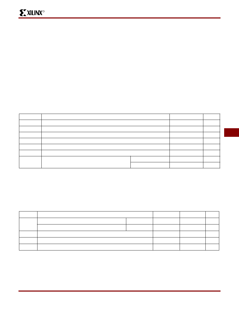
Absolute Maximum Ratings
Recommended Operating Conditions
Description
Units
V
CC
Supply voltage relative to Ground
-0.5 to 4.0
V
V
IN
Input voltage relative to Ground (Note 1)
-0.5 to 5.5
V
V
TS
Voltage applied to 3-state output (Note 1)
-0.5 to 5.5
V
V
CCt
Longest Supply Voltage Rise Time from 1 V to 3V
50
ms
T
STG
Storage temperature (ambient)
-65 to +150
�
C
T
SOL
Maximum soldering temperature (10 s @ 1/16 in. = 1.5 mm)
+260
�
C
T
J
Junction Temperature
Ceramic packages
+150
�
C
Plastic packages
+125
�
C
Note 1: Maximum DC excursion above V
cc
or below Ground must be limited to either 0.5 V or 10 mA, whichever is easier to
achieve. During transitions, the device pins may undershoot to -2.0 V or overshoot toV
CC
+2.0 V, provided this over or
undershoot lasts less than 10 ns and with the forcing current being limited to 200 mA.
Note:
Stresses beyond those listed under Absolute Maximum Ratings may cause permanent damage to the device. These are
stress ratings only, and functional operation of the device at these or any other conditions beyond those listed under
Recommended Operating Conditions is not implied. Exposure to Absolute Maximum Ratings conditions for extended
periods of time may affect device reliability.
Symbol
Description
Min
Max
Units
V
CC
Supply voltage relative to Gnd, T
J
= 0
�
C to +85
�
C
Commercial
3.0
3.6
V
Supply voltage relative to Gnd, T
J
= -40
�
C to +100
�
C
Industrial
3.0
3.6
V
V
IH
High-level input voltage
50% of V
CC
5.5
V
V
IL
Low-level input voltage
0
30% of V
CC
V
T
IN
Input signal transition time
250
ns
Notes:
At junction temperatures above those listed above, all delay parameters increase by 0.35% per
�
C.
Input and output measurement threshold is ~50% of V
CC
.

R
XC4000E and XC4000X Series Field Programmable Gate Arrays
6-74
DS005 (v. 1.8 October 18, 1999 - Product Specification
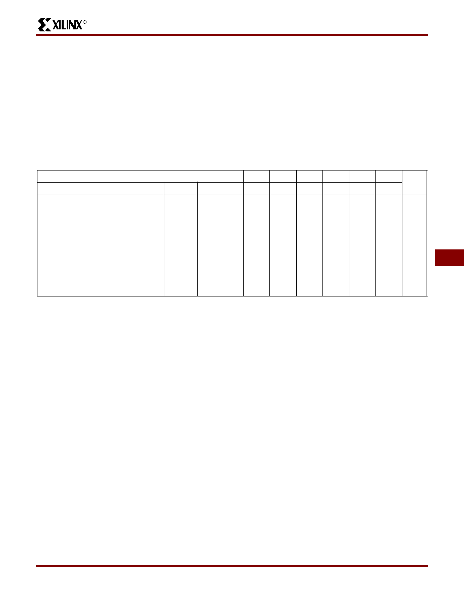
D.C. Characteristics Over Recommended Operating Conditions
Power-0n Power Supply Requirements
Xilinx FPGAs require a minimum rated power supply current capacity to insure proper initialization, and the power supply
ramp-up time does affect the current required. A fast ramp-up time requires more current than a slow ramp-up time. The
slowest ramp-up time is 50 ms. Current capacity is not specified for a ramp-up time faster than 2ms. The current capacity
varies linealy with ramp-up time,
e.g., an XC4036XL with a ramp-up time of 25 ms would require a capacity predicted by the
point on the straight line drawn from 1A at 120
�
s to 500 mA at 50 ms at the 25 ms time mark. This point is approximately
750 mA
.
Symbol
Description
Min
Max
Units
V
OH
High-level output voltage @ I
OH
= -4.0 mA, V
CC
min (LVTTL)
2.4
V
High-level output voltage @ I
OH
= -500
�
A, (LVCMOS)
90% V
CC
V
V
OL
Low-level output voltage @ I
OL
= 12.0 mA, V
CC
min (LVTTL) (Note 1)
0.4
V
Low-level output voltage @ I
OL
= 1500
�
A, (LVCMOS)
10% V
CC
V
V
DR
Data Retention Supply Voltage (below which configuration data may be lost)
2.5
V
I
CCO
Quiescent FPGA supply current (Note 2)
5
mA
I
L
Input or output leakage current
-10
+10
�
A
C
IN
Input capacitance (sample tested)
BGA, SBGA, PQ, HQ, MQ
packages
10
pF
PGA packages
16
pF
I
RPU
Pad pull-up (when selected) @ V
in
= 0 V (sample tested)
0.02
0.25
mA
I
RPD
Pad pull-down (when selected) @ V
in
= 3.6 V (sample tested)
0.02
0.15
mA
I
RLL
Horizontal Longline pull-up (when selected) @ logic Low
0.3
2.0
mA
Note 1:
With up to 64 pins simultaneously sinking 12 mA.
Note 2:
With no output current loads, no active input or Longline pull-up resistors, all I/O pins Tri-stated and floating.
Product
Description
Ramp-up Time
Fast (120
�
s)
Slow (50 ms)
XC4005 - 36XL
Minimum required current supply
1 A
500 mA
XC4044- 62XL
Minimum required current supply
2 A
500 mA
XC4085XL
1
Minimum required current supply
2 A
1
500 mA
Notes:
1.
The XC4085XL fast ramp-up time is 5 ms.
Devices are guaranteed to initialize properly with the minimum current listed above. A larger capacity power supply may
result in a larger initialization current.
This specification applies to Commercial and Industrial grade products only.
Ramp-up Time is measured from 0 V
DC
to 3.6 V
DC
. Peak current required lasts less than 3 ms, and occurs near the
internal power on reset threshold voltage. After initialization and before configuration, I
CC
max is less than 10 mA.
R
DS005 (v. 1.8 October 18, 1999 - Product Specification
6-75
XC4000E and XC4000X Series Field Programmable Gate Arrays
6
XC4000XL A.C. Characteristics
Testing of the switching parameters is modeled after testing methods specified by MIL-M-38510/605. All devices are 100%
functionally tested. Internal timing parameters are derived from measuring internal test patterns. Listed below are
representative values where one global clock input drives one vertical clock line in each accessible column, and where all
accessible IOB and CLB flip-flops are clocked by the global clock net.
When fewer vertical clock lines are connected, the clock distribution is faster; when multiple clock lines per column are driven
from the same global clock, the delay is longer. For more specific, more precise, and worst-case guaranteed data, reflecting
the actual routing structure, use the values provided by the static timing analyzer (TRCE in the Xilinx Development System)
and back-annotated to the simulation netlist. These path delays, provided as a guideline, have been extracted from the static
timing analyzer report. All timing parameters assume worst-case operating conditions (supply voltage and junction
temperature. Values apply to all XC4000XL devices and are expressed in nanoseconds unless otherwise noted.
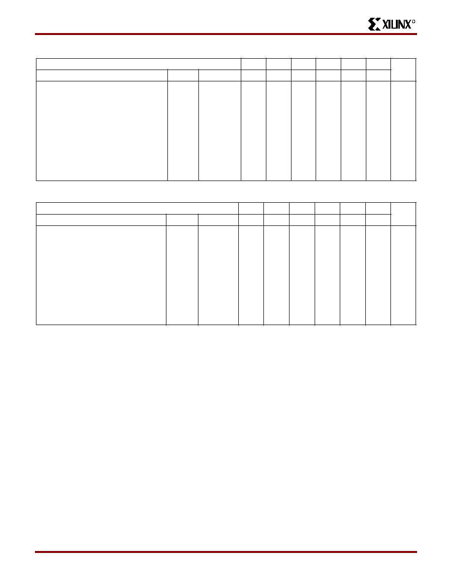
Global Low Skew Buffer to Clock K
Speed Grade
All
-3
-2
-1
-09
-08
Units
Description
Symbol
Device
Min
Max
Max
Max
Max
Max
Delay from pad through GLS buffer to
any clock input, K
T
GLS
XC4002XL
XC4005XL
XC4010XL
XC4013XL
XC4020XL
XC4028XL
XC4036XL
XC4044XL
XC4052XL
XC4062XL
XC4085XL
0.3
0.4
0.5
0.6
0.7
0.9
1.1
1.2
1.3
1.4
1.6
2.1
2.7
3.2
3.6
4.0
4.4
4.8
5.3
5.7
6.3
7.2
1.8
2.3
2.8
3.1
3.5
3.8
4.2
4.6
5.0
5.4
6.2
1.6
2.0
2.4
2.7
3.0
3.3
3.6
4.0
4.5
4.7
5.7
1.5
1.9
2.3
2.6
2.9
3.2
3.5
3.9
4.4
4.6
5.5
2.3
3.1
4.0
ns
ns
ns
ns
ns
ns
ns
ns
ns
ns
ns
R
XC4000E and XC4000X Series Field Programmable Gate Arrays
6-76
DS005 (v. 1.8 October 18, 1999 - Product Specification
Global Early BUFGEs 1, 2, 5, and 6 to IOB Clock
Global Early BUFGEs 3, 4, 7, and 8 to IOB Clock
Speed Grade
All
-3
-2
-1
-09
-08
Units
Description
Symbol
Device
Min
Max
Max
Max
Max
Max
Delay from pad through GE buffer to any
IOB clock input.
T
GE
XC4002XL
XC4005XL
XC4010XL
XC4013XL
XC4020XL
XC4028XL
XC4036XL
XC4044XL
XC4052XL
XC4062XL
XC4085XL
0.1
0.3
0.3
0.4
0.4
0.3
0.3
0.2
0.3
0.3
0.4
1.6
1.9
2.2
2.4
2.6
2.8
3.1
3.5
4.0
4.9
5.8
1.4
1.8
1.9
2.1
2.2
2.4
2.7
3.0
3.5
4.3
5.1
1.3
1.7
1.7
1.8
2.1
2.1
2.3
2.6
3.0
3.7
4.7
1.2
1.6
1.7
1.7
2.0
2.0
2.2
2.4
3.0
3.4
4.3
1.5
1.9
3.0
ns
ns
ns
ns
ns
ns
ns
ns
ns
ns
ns
Speed Grade
All
-3
-2
-1
-09
-08
Units
Description
Symbol
Device
Min
Max
Max
Max
Max
Max
Delay from pad through GE buffer to any
IOB clock input.
T
GE
XC4002XL
XC4005XL
XC4010XL
XC4013XL
XC4020XL
XC4028XL
XC4036XL
XC4044XL
XC4052XL
XC4062XL
XC4085XL
0.5
0.7
0.7
0.7
0.8
0.9
0.9
1.0
1.1
1.2
1.3
2.8
3.1
3.5
3.8
4.1
4.4
4.7
5.1
5.5
5.9
6.8
2.5
2.8
3.1
3.3
3.6
3.9
4.2
4.5
4.8
5.2
6.0
2.1
2.7
2.8
2.9
3.4
3.4
3.7
4.0
4.3
4.8
5.5
1.7
2.5
2.7
2.8
3.2
3.3
3.6
3.7
4.3
4.5
5.2
2.4
3.1
4.0
ns
ns
ns
ns
ns
ns
ns
ns
ns
ns
ns
R
DS005 (v. 1.8 October 18, 1999 - Product Specification
6-77
XC4000E and XC4000X Series Field Programmable Gate Arrays
6
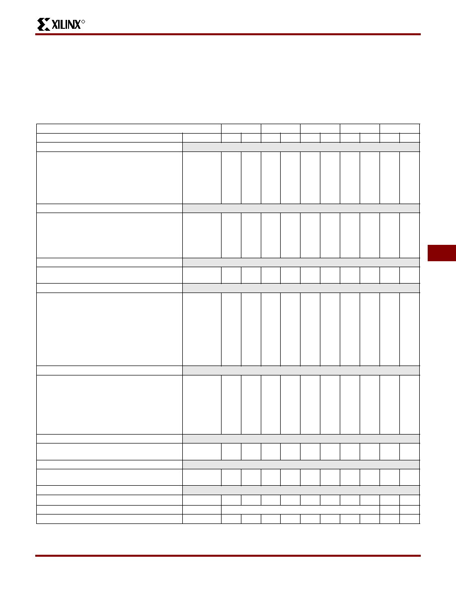
XC4000XL CLB Characteristics
Testing of switching parameters is modeled after testing methods specified by MIL-M-38510/605. All devices are 100%
functionally tested. Internal timing parameters are derived from measuring internal test patterns. Listed below are
representative values. For more specific, more precise, and worst-case guaranteed data, use the values reported by the
static timing analyzer (TRCE in the Xilinx Development System) and back-annotated to the simulation netlist. All timing
parameters assume worst-case operating conditions (supply voltage and junction temperature). Values apply to all
XC4000XL devices and are expressed in nanoseconds unless otherwise noted.
CLB Switching Characteristic Guidelines
Speed Grade
-3
-2
-1
-09
-08
Description
Symbol
Min
Max
Min
Max
Min
Max
Min
Max
Min
Max
Combinatorial Delays
F/G inputs to X/Y outputs
F/G inputs via H' to X/Y outputs
F/G inputs via transparent latch to Q outputs
C inputs via SR/H0 via H to X/Y outputs
C inputs via H1 via H to X/Y outputs
C inputs via DIN/H2 via H to X/Y outputs
C inputs via EC, DIN/H2 to YQ, XQ output (bypass)
T
ILO
T
IHO
T
ITO
T
HH0O
T
HH1O
T
HH2O
T
CBYP
1.6
2.7
2.9
2.5
2.4
2.5
1.5
1.5
2.4
2.6
2.2
2.1
2.2
1.3
1.3
2.2
2.2
2.0
1.9
2.0
1.1
1.2
2.0
2.0
1.8
1.6
1.8
1.0
1.1
1.9
1.8
1.8
1.5
1.8
0.9
CLB Fast Carry Logic
Operand inputs (F1, F2, G1, G4) to C
OUT
Add/Subtract input (F3) to C
OUT
Initialization inputs (F1, F3) to C
OUT
C
IN
through function generators to X/Y outputs
C
IN
to C
OUT
, bypass function generators
Carry Net Delay, C
OUT
to C
IN
T
OPCY
T
ASCY
T
INCY
T
SUM
T
BYP
T
NET
2.7
3.3
2.0
2.8
0.26
0.32
2.3
2.9
1.8
2.6
0.23
0.28
2.0
2.5
1.5
2.4
0.20
0.25
1.6
1.8
1.0
1.7
0.14
0.24
1.6
1.8
0.9
1.5
0.14
0.24
Sequential Delays
Clock K to Flip-Flop outputs Q
Clock K to Latch outputs Q
T
CKO
T
CKLO
2.1
2.1
1.9
1.9
1.6
1.6
1.5
1.5
1.4
1.4
Setup Time before Clock K
F/G inputs
F/G inputs via H
C inputs via H0 through H
C inputs via H1 through H
C inputs via H2 through H
C inputs via DIN
C inputs via EC
C inputs via S/R, going Low (inactive)
CIN input via F/G
CIN input via F/G and H
T
ICK
T
IHCK
T
HH0CK
T
HH1CK
T
HH2CK
T
DICK
T
ECCK
T
RCK
T
CCK
T
CHCK
1.1
2.2
2.0
1.9
2.0
0.9
1.0
0.6
2.3
3.4
1.0
1.9
1.7
1.6
1.7
0.8
0.9
0.5
2.1
3.0
0.9
1.7
1.6
1.4
1.6
0.7
0.8
0.5
1.9
2.7
0.8
1.6
1.4
1.2
1.4
0.6
0.7
0.4
1.3
2.1
0.8
1.5
1.4
1.1
1.4
0.6
0.7
0.4
1.2
2.0
Hold Time after Clock K
F/G inputs
F/G inputs via H
C inputs via SR/H0 through H
C inputs via H1 through H
C inputs via DIN/H2 through H
C inputs via DIN/H2
C inputs via EC
C inputs via SR, going Low (inactive)
T
CKI
T
CKIH
T
CKHH0
T
CKHH1
T
CKHH2
T
CKDI
T
CKEC
T
CKR
0
0
0
0
0
0
0
0
0
0
0
0
0
0
0
0
0
0
0
0
0
0
0
0
0
0
0
0
0
0
0
0
0
0
0
0
0
0
0
0
Clock
Clock High time
Clock Low time
T
CH
T
CL
3.0
3.0
2.8
2.8
2.5
2.5
2.3
2.3
2.1
2.1
Set/Reset Direct
Width (High)
Delay from C inputs via S/R, going High to Q
T
RPW
T
RIO
3.0
3.7
2.8
3.2
2.5
2.8
2.3
2.7
2.3
2.6
Global Set/Reset
Minimum GSR Pulse Width
T
MRW
19.8
17.3
15.0
14.0
14.0
Delay from GSR input to any Q
T
MRQ
See
Table on page 85
for T
RRI
values per device.
Toggle Frequency (MHz) (for export control)
F
TOG
(MHz)
166
179
200
217
238