November 5, 1998 (Version 5.2)
7-83
7
Features
∑ Low-cost, register/latch rich, SRAM based
reprogrammable architecture
-
0.5
µ
m three-layer metal CMOS process technology
-
256 to 1936 logic cells (3,000 to 23,000 "gates")
-
Price competitive with Gate Arrays
∑
System Level Features
-
System performance beyond 50 MHz
-
6 levels of interconnect hierarchy
-
VersaRing
TM
I/O Interface for pin-locking
-
Dedicated carry logic for high-speed arithmetic
functions
-
Cascade chain for wide input functions
-
Built-in IEEE 1149.1 JTAG boundary scan test
circuitry on all I/O pins
-
Internal 3-state bussing capability
-
Four dedicated low-skew clock or signal distribution
nets
∑
Versatile I/O and Packaging
-
Innovative VersaRing
TM
I/O interface provides a high
logic cell to I/O ratio, with up to 244 I/O signals
-
Programmable output slew-rate control maximizes
performance and reduces noise
-
Zero Flip-Flop hold time for input registers simplifies
system timing
-
Independent Output Enables for external bussing
-
Footprint compatibility in common packages within
the XC5200 Series and with the XC4000 Series
-
Over 150 device/package combinations, including
advanced BGA, TQ, and VQ packaging available
∑
Fully Supported by Xilinx Development System
-
Automatic place and route software
-
Wide selection of PC and Workstation platforms
-
Over 100 3rd-party Alliance interfaces
-
Supported by shrink-wrap Foundation software
Description
The XC5200 Field-Programmable Gate Array Family is
engineered to deliver low cost. Building on experiences
gained with three previous successful SRAM FPGA fami-
lies, the XC5200 family brings a robust feature set to pro-
grammable logic design. The VersaBlock
TM
logic module,
the VersaRing I/O interface, and a rich hierarchy of inter-
connect resources combine to enhance design flexibility
and reduce time-to-market. Complete support for the
XC5200 family is delivered through the familiar Xilinx soft-
ware environment. The XC5200 family is fully supported on
popular workstation and PC platforms. Popular design
entry methods are fully supported, including ABEL, sche-
matic capture, VHDL, and Verilog HDL synthesis. Design-
ers utilizing logic synthesis can use their existing tools to
design with the XC5200 devices.
.
0
XC5200 Series
Field Programmable Gate Arrays
November 5, 1998 (Version 5.2)
0
7*
Product Specification
R
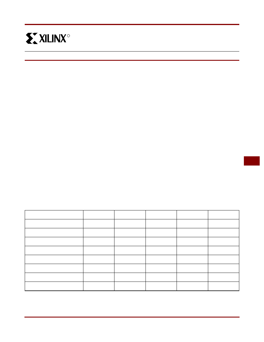
Table 1: XC5200 Field-Programmable Gate Array Family Members
Device
XC5202
XC5204
XC5206
XC5210
XC5215
Logic Cells
256
480
784
1,296
1,936
Max Logic Gates
3,000
6,000
10,000
16,000
23,000
Typical Gate Range
2,000 - 3,000
4,000 - 6,000
6,000 - 10,000
10,000 - 16,000 15,000 - 23,000
VersaBlock Array
8 x 8
10 x 12
14 x 14
18 x 18
22 x 22
CLBs
64
120
196
324
484
Flip-Flops
256
480
784
1,296
1,936
I/Os
84
124
148
196
244
TBUFs per Longline
10
14
16
20
24
R
XC5200 Series Field Programmable Gate Arrays
7-84
November 5, 1998 (Version 5.2)
XC5200 Family Compared to
XC4000/SpartanTM and XC3000
Series
For readers already familiar with the XC4000/Spartan and
XC3000 FPGA Families, this section describes significant
differences between them and the XC5200 family. Unless
otherwise indicated, comparisons refer to both
XC4000/Spartan and XC3000 devices.
Configurable Logic Block (CLB) Resources
Each XC5200 CLB contains four independent 4-input func-
tion generators and four registers, which are configured as
four independent Logic CellsTM (LCs). The registers in each
XC5200 LC are optionally configurable as edge-triggered
D-type flip-flops or as transparent level-sensitive latches.
The XC5200 CLB includes dedicated carry logic that pro-
vides fast arithmetic carry capability. The dedicated carry
logic may also be used to cascade function generators for
implementing wide arithmetic functions.
XC4000 family:
XC5200 devices have no wide edge
decoders. Wide decoders are implemented using cascade
logic. Although sacrificing speed for some designs, lack of
wide edge decoders reduces the die area and hence cost
of the XC5200.
XC4000/Spartan family:
XC5200 dedicated carry logic
differs from that of the XC4000/Spartan family in that the
sum is generated in an additional function generator in the
adjacent column. This design reduces XC5200 die size and
hence cost for many applications. Note, however, that a
loadable up/down counter requires the same number of
function generators in both families. XC3000 has no dedi-
cated carry.
XC4000/Spartan family: XC5200 lookup tables are opti-
mized for cost and hence cannot implement RAM.
Input/Output Block (IOB) Resources
The XC5200 family maintains footprint compatibility with
the XC4000 family, but not with the XC3000 family.
To minimize cost and maximize the number of I/O per Logic
Cell, the XC5200 I/O does not include flip-flops or latches.
For high performance paths, the XC5200 family provides
direct connections from each IOB to the registers in the
adjacent CLB in order to emulate IOB registers.
Each XC5200 I/O Pin provides a programmable delay ele-
ment to control input set-up time. This element can be used
to avoid potential hold-time problems. Each XC5200 I/O
Pin is capable of 8-mA source and sink currents.
IEEE 1149.1-type boundary scan is supported in each
XC5200 I/O.
Routing Resources
The XC5200 family provides a flexible coupling of logic and
local routing resources called the VersaBlock. The XC5200
VersaBlock element includes the CLB, a Local Interconnect
Matrix (LIM), and direct connects to neighboring Versa-
Blocks.
The XC5200 provides four global buffers for clocking or
high-fanout control signals. Each buffer may be sourced by
means of its dedicated pad or from any internal source.
Each XC5200 TBUF can drive up to two horizontal and two
vertical Longlines. There are no internal pull-ups for
XC5200 Longlines.
Configuration and Readback
The XC5200 supports a new configuration mode called
Express mode.
XC4000/Spartan family:
The XC5200 family provides a
global reset but not a global set.
XC5200 devices use a different configuration process than
that of the XC3000 family, but use the same process as the
XC4000 and Spartan families.
XC3000 family: Although their configuration processes dif-
fer, XC5200 devices may be used in daisy chains with
XC3000 devices.
XC3000 family: The XC5200 PROGRAM pin is a sin-
gle-function input pin that overrides all other inputs. The
PROGRAM pin does not exist in XC3000.
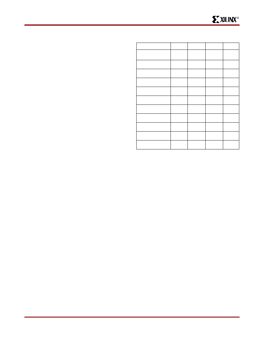
Table 2: Xilinx Field-Programmable Gate Array
Families
Parameter
XC5200 Spartan XC4000 XC3000
CLB function
generators
4
3
3
2
CLB inputs
20
9
9
5
CLB outputs
12
4
4
2
Global buffers
4
8
8
2
User RAM
no
yes
yes
no
Edge decoders
no
no
yes
no
Cascade chain
yes
no
no
no
Fast carry logic
yes
yes
yes
no
Internal 3-state
yes
yes
yes
yes
Boundary scan
yes
yes
yes
no
Slew-rate control
yes
yes
yes
yes
R
November 5, 1998 (Version 5.2)
7-85
XC5200 Series Field Programmable Gate Arrays
7
XC3000 family: XC5200 devices support an additional pro-
gramming mode: Peripheral Synchronous.
XC3000 family: The XC5200 family does not support
Power-down, but offers a Global 3-state input that does not
reset any flip-flops.
XC3000 family: The XC5200 family does not provide an
on-chip crystal oscillator amplifier, but it does provide an
internal oscillator from which a variety of frequencies up to
12 MHz are available.
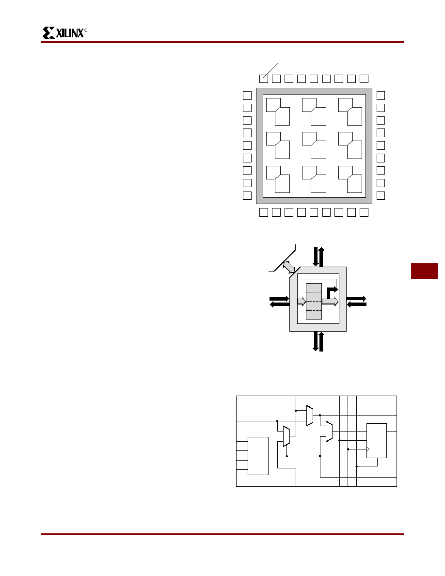
Architectural Overview
Figure 1
presents a simplified, conceptual overview of the
XC5200 architecture. Similar to conventional FPGAs, the
XC5200 family consists of programmable IOBs, program-
mable logic blocks, and programmable interconnect. Unlike
other FPGAs, however, the logic and local routing
resources of the XC5200 family are combined in flexible
VersaBlocks (
Figure 2
). General-purpose routing connects
to the VersaBlock through the General Routing Matrix
(GRM).
VersaBlock: Abundant Local Routing Plus
Versatile Logic
The basic logic element in each VersaBlock structure is the
Logic Cell, shown in
Figure 3
. Each LC contains a 4-input
function generator (F), a storage device (FD), and control
logic. There are five independent inputs and three outputs
to each LC. The independence of the inputs and outputs
allows the software to maximize the resource utilization
within each LC. Each Logic Cell also contains a direct
feedthrough path that does not sacrifice the use of either
the function generator or the register; this feature is a first
for FPGAs. The storage device is configurable as either a D
flip-flop or a latch. The control logic consists of carry logic
for fast implementation of arithmetic functions, which can
also be configured as a cascade chain allowing decode of
very wide input functions.
Figure 1: XC5200 Architectural Overview
Figure 2: VersaBlock
Figure 3: XC5200 Logic Cell (Four LCs per CLB)
X4955
GRM
Input/Output Blocks (IOBs)
Versa-
Block
GRM
Versa-
Block
VersaRing
VersaRing
GRM
Versa-
Block
GRM
Versa-
Block
GRM
Versa-
Block
GRM
Versa-
Block
GRM
Versa-
Block
GRM
Versa-
Block
GRM
Versa-
Block
VersaRing
VersaRing
X5707
CLB
Direct Connects
TS
GRM
LIM
4
4
4
4
4
LC3
LC2
LC1
LC0
4
4
4
4
24
24
X4956
F4
F3
F
FD
F2
F1
D
Q
X
DO
DI
CO
CI
CE CK
CLR
R
XC5200 Series Field Programmable Gate Arrays
7-86
November 5, 1998 (Version 5.2)
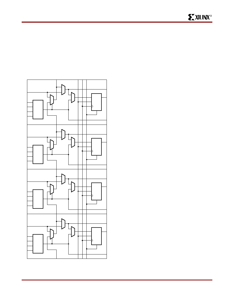
The XC5200 CLB consists of four LCs, as shown in
Figure 4
. Each CLB has 20 independent inputs and 12
independent outputs. The top and bottom pairs of LCs can
be configured to implement 5-input functions. The chal-
lenge of FPGA implementation software has always been
to maximize the usage of logic resources. The XC5200
family addresses this issue by surrounding each CLB with
two types of local interconnect -- the Local Interconnect
Matrix (LIM) and direct connects. These two interconnect
resources, combined with the CLB, form the VersaBlock,
represented in
Figure 2
.
The LIM provides 100% connectivity of the inputs and out-
puts of each LC in a given CLB. The benefit of the LIM is
that no general routing resources are required to connect
feedback paths within a CLB. The LIM connects to the
GRM via 24 bidirectional nodes.
The direct connects allow immediate connections to neigh-
boring CLBs, once again without using any of the general
interconnect. These two layers of local routing resource
improve the granularity of the architecture, effectively mak-
ing the XC5200 family a "sea of logic cells." Each
Versa-Block has four 3-state buffers that share a common
enable line and directly drive horizontal and vertical Lon-
glines, creating robust on-chip bussing capability. The
VersaBlock allows fast, local implementation of logic func-
tions, effectively implementing user designs in a hierarchi-
cal fashion. These resources also minimize local routing
congestion and improve the efficiency of the general inter-
connect, which is used for connecting larger groups of
logic. It is this combination of both fine-grain and
coarse-grain architecture attributes that maximize logic uti-
lization in the XC5200 family. This symmetrical structure
takes full advantage of the third metal layer, freeing the
placement software to pack user logic optimally with mini-
mal routing restrictions.
VersaRing I/O Interface
The interface between the IOBs and core logic has been
redesigned in the XC5200 family. The IOBs are completely
decoupled from the core logic. The XC5200 IOBs contain
dedicated boundary-scan logic for added board-level test-
ability, but do not include input or output registers. This
approach allows a maximum number of IOBs to be placed
around the device, improving the I/O-to-gate ratio and
decreasing the cost per I/O. A "freeway" of interconnect
cells surrounding the device forms the VersaRing, which
provides connections from the IOBs to the internal logic.
These incremental routing resources provide abundant
connections from each IOB to the nearest VersaBlock, in
addition to Longline connections surrounding the device.
The VersaRing eliminates the historic trade-off between
high logic utilization and pin placement flexibility. These
incremental edge resources give users increased flexibility
in preassigning (i.e., locking) I/O pins before completing
their logic designs. This ability accelerates time-to-market,
since PCBs and other system components can be manu-
factured concurrent with the logic design.
General Routing Matrix
The GRM is functionally similar to the switch matrices
found in other architectures, but it is novel in its tight cou-
pling to the logic resources contained in the VersaBlocks.
Advanced simulation tools were used during the develop-
ment of the XC5200 architecture to determine the optimal
level of routing resources required. The XC5200 family
contains six levels of interconnect hierarchy -- a series of
Figure 4: Configurable Logic Block
X4957
F4
F3
F
FD
LC3
LC2
LC1
LC0
F2
F1
D
Q
X
DO
DI
CO
F4
F3
F
FD
F2
F1
D
Q
X
DO
DI
F4
F3
F
FD
F2
F1
D
Q
X
DO
DI
F4
F3
F
FD
F2
F1
D
Q
X
DO
DI
CI
CE CK
CLR
LC0
R
November 5, 1998 (Version 5.2)
7-87
XC5200 Series Field Programmable Gate Arrays
7
single-length lines, double-length lines, and Longlines all
routed through the GRM. The direct connects, LIM, and
logic-cell feedthrough are contained within each
Versa-Block. Throughout the XC5200 interconnect, an effi-
cient multiplexing scheme, in combination with three layer
metal (TLM), was used to improve the overall efficiency of
silicon usage.
Performance Overview
The XC5200 family has been benchmarked with many
designs running synchronous clock rates beyond 66 MHz.
The performance of any design depends on the circuit to be
implemented, and the delay through the combinatorial and
sequential logic elements, plus the delay in the intercon-
nect routing. A rough estimate of timing can be made by
assuming 3-6 ns per logic level, which includes direct-con-
nect routing delays, depending on speed grade. More
accurate estimations can be made using the information in
the Switching Characteristic Guideline section.
Taking Advantage of Reconfiguration
FPGA devices can be reconfigured to change logic function
while resident in the system. This capability gives the sys-
tem designer a new degree of freedom not available with
any other type of logic.
Hardware can be changed as easily as software. Design
updates or modifications are easy, and can be made to
products already in the field. An FPGA can even be recon-
figured dynamically to perform different functions at differ-
ent times.
Reconfigurable logic can be used to implement system
self-diagnostics, create systems capable of being reconfig-
ured for different environments or operations, or implement
multi-purpose hardware for a given application. As an
added benefit, using reconfigurable FPGA devices simpli-
fies hardware design and debugging and shortens product
time-to-market.
Detailed Functional Description
Configurable Logic Blocks (CLBs)
Figure 4
shows the logic in the XC5200 CLB, which con-
sists of four Logic Cells (LC[3:0]). Each Logic Cell consists
of an independent 4-input Lookup Table (LUT), and a
D-Type flip-flop or latch with common clock, clock enable,
and clear, but individually selectable clock polarity. Addi-
tional logic features provided in the CLB are:
∑ An independent 5-input LUT by combining two 4-input
LUTs.
∑ High-speed carry propagate logic.
∑ High-speed pattern decoding.
∑ High-speed direct connection to flip-flop D-inputs.
∑
Individual selection of either a transparent,
level-sensitive latch or a D flip-flop.
∑
Four 3-state buffers with a shared Output Enable.
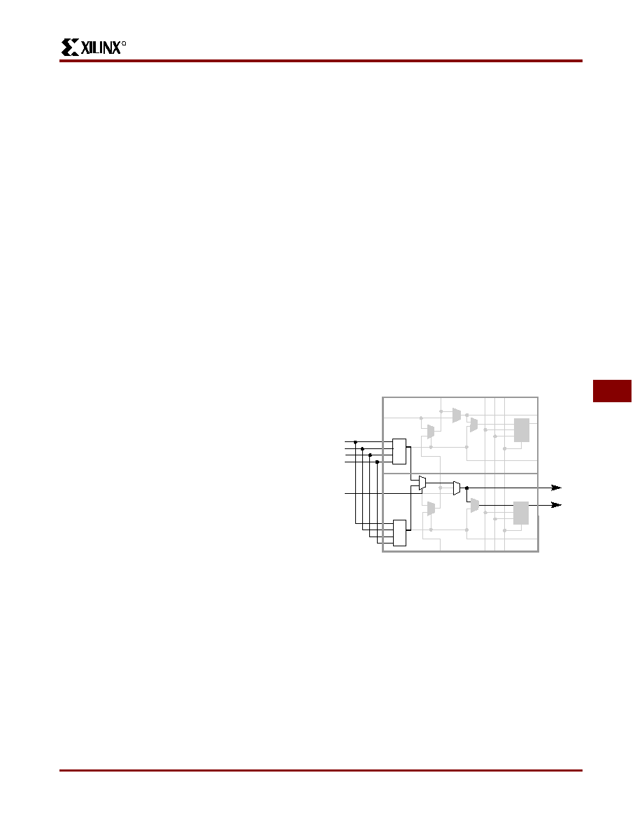
5-Input Functions
Figure 5
illustrates how the outputs from the LUTs from
LC0 and LC1 can be combined with a 2:1 multiplexer
(F5_MUX) to provide a 5-input function. The outputs from
the LUTs of LC2 and LC3 can be similarly combined.
Figure 5: Two LUTs in Parallel Combined to Create a
5-input Function
out
Q
Qout
DO
Q
D
FD
X
FD
CO
DI
X
CLR
LC0
CK
CE
5-Input Function
D
DO
F5_MUX
DI
F
F4
F3
F2
F1
F4
F3
F2
F1
I1
I2
I3
I4
I5
CI
F
LC1
X5710