 | –≠–ª–µ–∫—Ç—Ä–æ–Ω–Ω—ã–π –∫–æ–º–ø–æ–Ω–µ–Ω—Ç: XC9500XL | –°–∫–∞—á–∞—Ç—å:  PDF PDF  ZIP ZIP |
DS054 (v1.6) January 24, 2002
www.xilinx.com
1
Preliminary Product Specification
1-800-255-7778
© 2002 Xilinx, Inc. All rights reserved. All Xilinx trademarks, registered trademarks, patents, and disclaimers are as listed at
http://www.xilinx.com/legal.htm
.
All other trademarks and registered trademarks are the property of their respective owners. All specifications are subject to change without notice.
k
Features
∑
Optimized for high-performance 3.3V systems
-
5 ns pin-to-pin logic delays, with internal system
frequency up to 208 MHz
-
Small footprint packages including VQFPs, TQFPs
and CSPs (Chip Scale Package)
-
Lower power operation
-
5V tolerant I/O pins accept 5V, 3.3V, and 2.5V
signals
-
3.3V or 2.5V output capability
-
Advanced 0.35 micron feature size CMOS
FastFLASH technology
∑
Advanced system features
-
In-system programmable
-
Superior pin-locking and routability with
FastCONNECT IITM switch matrix
-
Extra wide 54-input Function Blocks
-
Up to 90 product-terms per macrocell with
individual product-term allocation
-
Local clock inversion with three global and one
product-term clocks
-
Individual output enable per output pin with local
inversion
-
Input hysteresis on all user and boundary-scan pin
inputs
-
Bus-hold circuitry on all user pin inputs
-
Supports hot-plugging capability
-
Full IEEE Standard 1149.1 boundary-scan (JTAG)
support on all devices
∑
Four pin-compatible device densities
-
36 to 288 macrocells, with 800 to 6400 usable
gates
∑
Fast concurrent programming
∑
Slew rate control on individual outputs
∑
Enhanced data security features
∑
Excellent quality and reliability
-
10,000 program/erase cycles endurance rating
-
20 year data retention
∑
Pin-compatible with 5V core XC9500 family in common
package footprints
0
XC9500XL High-Performance CPLD
Family
DS054 (v1.6) January 24, 2002
0
0
Preliminary Product Specification
R
Table 1: XC9500XL Device Family
XC9536XL
XC9572XL
XC95144XL
XC95288XL
Macrocells
36
72
144
288
Usable Gates
800
1,600
3,200
6,400
Registers
36
72
144
288
T
PD
(ns)
5
5
5
6
T
SU
(ns)
3.7
3.7
3.7
4.0
T
CO
(ns)
3.5
3.5
3.5
3.8
f
SYSTEM
(MHz)
178
178
178
208

XC9500XL High-Performance CPLD Family
2
www.xilinx.com
DS054 (v1.6) January 24, 2002
1-800-255-7778
Preliminary Product Specification
R
Table 2: XC9500XL Packages and User I/O Pins (not including 4 dedicated JTAG pins)
XC9536XL
XC9572XL
XC95144XL
XC95288XL
44-pin PLCC
34
34
-
-
44-pin VQFP
34
34
-
-
48-pin 0.8 mm CSP
36
38
-
-
64-pin VQFP
36
52
-
-
100-pin TQFP
-
72
81
-
144-pin 0.8 mm CSP
-
-
117
-
144-pin TQFP
-
-
117
117
208-pin PQFP
-
-
-
168
256-pin BGA
-
-
-
192
256-pin FBGA
-
-
-
192
280-pin 0.8 mm CSP
-
-
-
192
Figure 1: XC9500XL Architecture
Note: Function block outputs (indicated by the bold lines) drive the I/O blocks directly.
In-System Programming Controller
JTAG
Controller
I/O
Blocks
Function
Block 1
Macrocells
1 to 18
Macrocells
1 to 18
Macrocells
1 to 18
Macrocells
1 to 18
JTAG Port
3
54
I/O/GTS
I/O/GSR
I/O/GCK
I/O
I/O
I/O
I/O
2 or 4
1
I/O
I/O
I/O
I/O
3
DS054_01_042001
Function
Block 2
54
Function
Block 3
54
18
18
18
18
Function
Block N
54
FastCONNECT II Switch Matrix
XC9500XL High-Performance CPLD Family
DS054 (v1.6) January 24, 2002
www.xilinx.com
3
Preliminary Product Specification
1-800-255-7778
R
Family Overview
The FastFLASH XC9500XL family is a 3.3V CPLD family
targeted for high-performance, low-voltage applications in
leading-edge communications and computing systems,
where high device reliability and low power dissipation is
important. Each XC9500XL device supports in-system pro-
gramming (ISP) and the full IEEE 1149.1 (JTAG) bound-
ary-scan, allowing superior debug and design iteration
capability for small form-factor packages. The XC9500XL
family is designed to work closely with the Xilinx Virtex,
Spartan-XL and XC4000XL FPGA families, allowing system
designers to partition logic optimally between fast interface
circuitry and high-density general purpose logic. As shown
in
Table 1
, logic density of the XC9500XL devices ranges
from 800 to 6400 usable gates with 36 to 288 registers,
respectively. Multiple package options and associated I/O
capacity are shown in
Table 2
. The XC9500XL family mem-
bers are fully pin-compatible, allowing easy design migra-
tion across multiple density options in a given package
footprint.
The XC9500XL architectural features address the require-
ments of in-system programmability. Enhanced pin-locking
capability avoids costly board rework. In-system program-
ming throughout the full commercial operating range and a
high programming endurance rating provide worry-free
reconfigurations of system field upgrades. Extended data
retention supports longer and more reliable system operat-
ing life.
Advanced system features include output slew rate control
and user-programmable ground pins to help reduce system
noise. Each user pin is compatible with 5V, 3.3V, and 2.5V
inputs, and the outputs may be configured for 3.3V or 2.5V
operation. The XC9500XL device exhibits symmetric full
3.3V output voltage swing to allow balanced rise and fall
times.
Architecture Description
Each XC9500XL device is a subsystem consisting of multi-
ple Function Blocks (FBs) and I/O Blocks (IOBs) fully inter-
connected by the FastCONNECT II switch matrix. The IOB
provides buffering for device inputs and outputs. Each FB
provides programmable logic capability with extra wide
54inputs and 18 outputs. The FastCONNECT II switch
matrix connects all FB outputs and input signals to the FB
inputs. For each FB, up to 18 outputs (depending on pack-
age pin-count) and associated output enable signals drive
directly to the IOBs. See
Figure 1
Function Block
Each Function Block, as shown in
Figure 2
is comprised of
18 independent macrocells, each capable of implementing
a combinatorial or registered function. The FB also receives
global clock, output enable, and set/reset signals. The FB
generates 18 outputs that drive the FastCONNECT switch
matrix. These 18 outputs and their corresponding output
enable signals also drive the IOB.
Logic within the FB is implemented using a sum-of-products
representation. Fifty-four inputs provide 108 true and com-
plement signals into the programmable AND-array to form
90 product terms. Any number of these product terms, up to

XC9500XL High-Performance CPLD Family
4
www.xilinx.com
DS054 (v1.6) January 24, 2002
1-800-255-7778
Preliminary Product Specification
R
the 90 available, can be allocated to each macrocell by the
product term allocator.
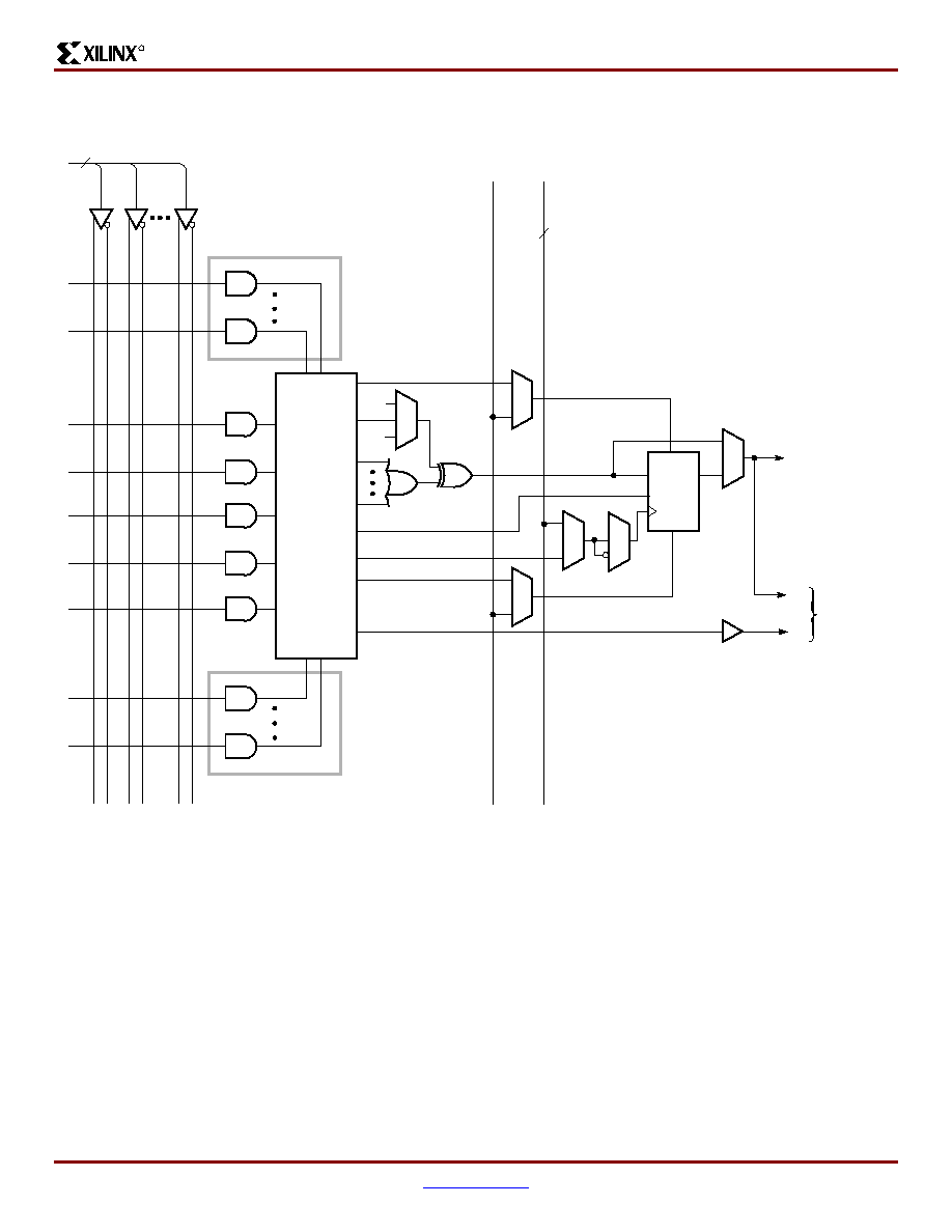
Macrocell
Each XC9500XL macrocell may be individually configured
for a combinatorial or registered function. The macrocell
and associated FB logic is shown in
Figure 3
.
Five direct product terms from the AND-array are available
for use as primary data inputs (to the OR and XOR gates) to
implement combinatorial functions, or as control inputs
including clock, clock enable, set/reset, and output enable.
The product term allocator associated with each macrocell
selects how the five direct terms are used.
The macrocell register can be configured as a D-type or
T-type flip-flop, or it may be bypassed for combinatorial
operation. Each register supports both asynchronous set
and reset operations. During power-up, all user registers
Figure 2: XC9500XL Function Block
Macrocell 18
Macrocell 1
Programmable
AND-Array
Product
Term
Allocators
From
FastCONNECT II
Switch Matrix
DS054_02_042101
54
1
To FastCONNECT II
Switch Matrix
To I/O Blocks
OUT
Global
Set/Reset
3
18
PTOE
18
18
Global
Clocks
XC9500XL High-Performance CPLD Family
DS054 (v1.6) January 24, 2002
www.xilinx.com
5
Preliminary Product Specification
1-800-255-7778
R
are initialized to the user-defined preload state (default to 0
if unspecified).
All global control signals are available to each individual
macrocell, including clock, set/reset, and output enable sig-
nals. As shown in
Figure 4
, the macrocell register clock
originates from either of three global clocks or a product
term clock. Both true and complement polarities of the
selected clock source can be used within each macrocell. A
GSR input is also provided to allow user registers to be set
to a user-defined state.
Figure 3: XC9500XL Macrocell Within Function Block
DS054_03_042101
To
FastCONNECTII
Switch Matrix
Additional
Product
Terms
(from other
macrocells)
Global
Set/Reset
Global
Clocks
Additional
Product
Terms
(from other
macrocells)
To
I/O Blocks
OUT
1
0
54
3
PTOE
D/T Q
S
R
Product
Term
Allocator
Product Term Set
Product Term Clock
Product Term Reset
Product Term OE
Product Term Clock Enable
CE