September 15, 1999 (Version 4.0)
1
Features
∑
10 ns pin-to-pin logic delays on all pins
∑
f
CNT
to 95 MHz
∑
288 macrocells with 6,400 usable gates
∑
Up to 192 user I/O pins
∑
5 V in-system programmable
-
Endurance of 10,000 program/erase cycles
-
Program/erase over full commercial voltage and
temperature range
∑
Enhanced pin-locking architecture
∑
Flexible 36V18 Function Block
-
90 product terms drive any or all of 18 macrocells
within Function Block
-
Global and product term clocks, output enables, set
and reset signals
∑
Extensive IEEE Std 1149.1 boundary-scan (JTAG)
support
∑
Programmable power reduction mode in each
macrocell
∑
Slew rate control on individual outputs
∑
User programmable ground pin capability
∑
Extended pattern security features for design protection
∑
High-drive 24 mA outputs
∑
3.3 V or 5 V I/O capability
∑
Advanced CMOS 5V FastFLASH technology
∑
Supports parallel programming of more than one
XC9500 concurrently
∑
Available in 352-pin BGA and 208-pin HQFP packages
Description
The XC95288 is a high-performance CPLD providing
advanced in-system programming and test capabilities for
general purpose logic integration. It is comprised of sixteen
36V18 Function Blocks, providing 6,400 usable gates with
propagation delays of 10 ns. See
Figure 2
for the architec-
ture overview.
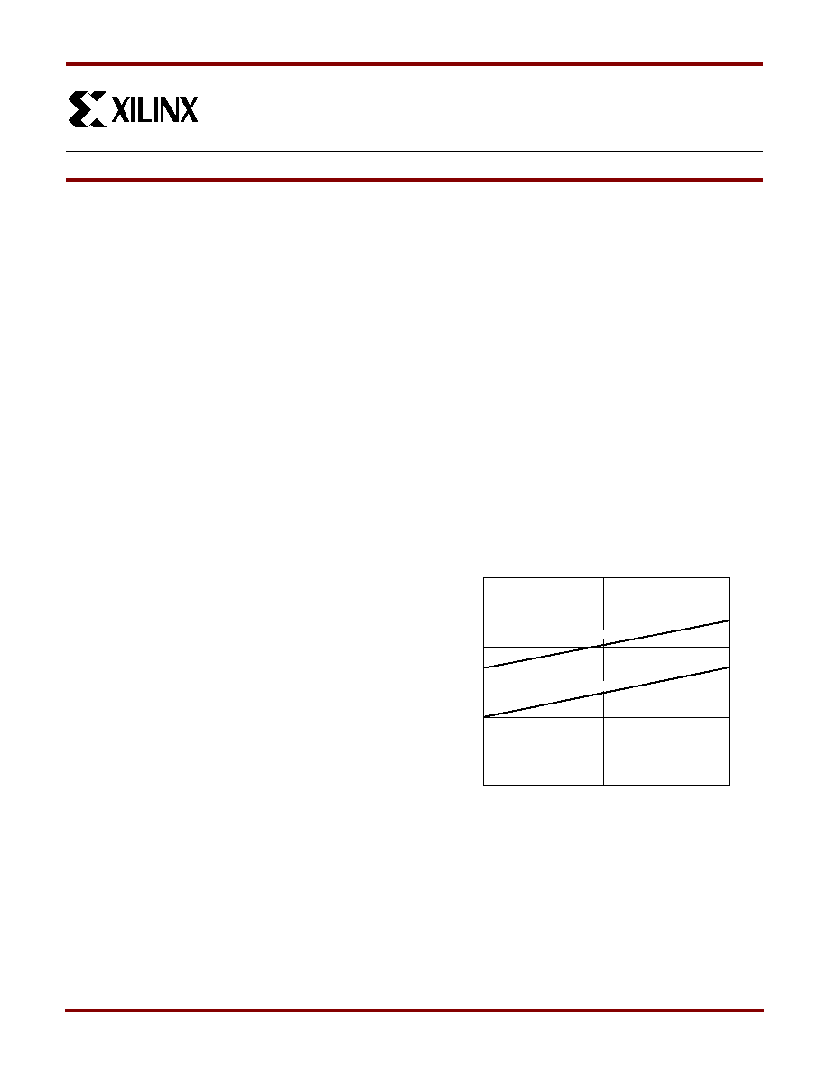
Power Management
Power dissipation can be reduced in the XC95288 by con-
figuring macrocells to standard or low-power modes of
operation. Unused macrocells are turned off to minimize
power dissipation.
Operating current for each design can be approximated for
specific operating conditions using the following equation:
I
CC
(mA) =
MC
HP
(1.7) + MC
LP
(0.9) + MC (0.006 mA/MHz) f
Where:
MC
HP
= Macrocells in high-performance mode
MC
LP
= Macrocells in low-power mode
MC = Total number of macrocells used
f = Clock frequency (MHz)
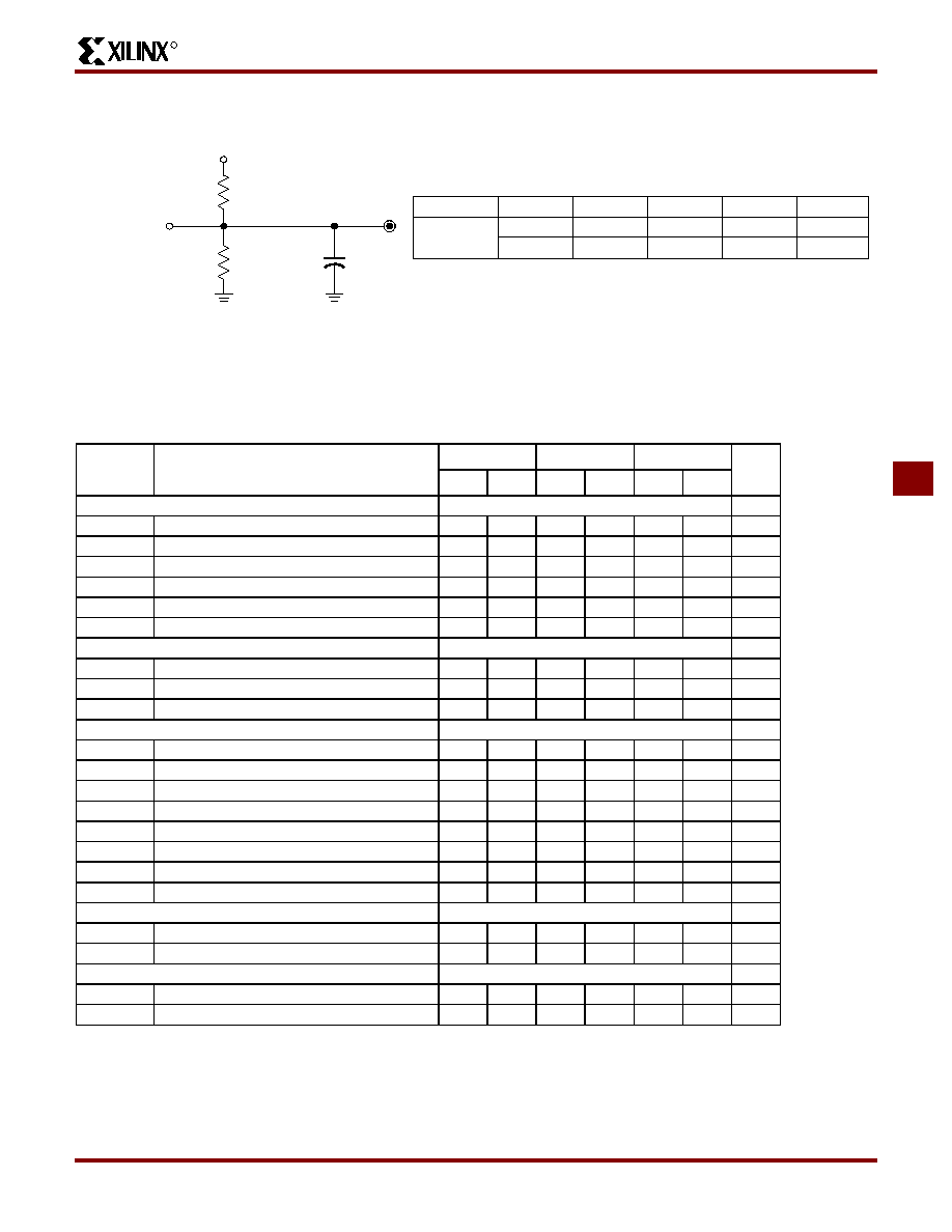
Figure 1
shows a typical calculation for the XC95288
device.
0
XC95288 In-System Programmable
CPLD
September 15, 1999 (Version 4.0)
0
5*
Product Specification
Æ
Clock Frequency (MHz)
Typical I
CC
(mA)
0
50
300
(500)
(700)
(500)
600
900
100
High Performance
Low Power
X7131
Figure 1: Typical I
CC
vs. Frequency For XC95288
R
XC95288 In-System Programmable CPLD
2
September 15, 1999 (Version 4.0)
In-System Programming Controller
JTAG
Controller
I/O
Blocks
Function
Block 1
Macrocells
1 to 18
Macrocells
1 to 18
Macrocells
1 to 18
Macrocells
1 to 18
JTAG Port
3
36
I/O/GTS
I/O/GSR
I/O/GCK
I/O
I/O
I/O
I/O
2
1
I/O
I/O
I/O
I/O
3
X5924
1
Function
Block 2
36
Function
Block 3
36
Function
Block 4
36
Macrocells
1 to 18
Function
Block 16
36
18
18
18
18
18
FastCONNECT Switch Matrix
Figure 2: XC95288 Architecture
Note: Function Block outputs (indicated by the bold line) drive the I/O Blocks directly
R
September 15, 1999 (Version 4.0)
3
XC95288 In-System Programmable CPLD
5
Absolute Maximum Ratings
Warning:
Stresses beyond those listed under Absolute Maximum Ratings may cause permanent damage to the device. These are
stress ratings only, and functional operation of the device at these or any other conditions beyond those listed under
Recommended Operating Conditions is not implied. Exposure to Absolute Maximum Rating conditions for extended periods
of time may affect device reliability.
Recommended Operation Conditions
1
Note:
1. Numbers in parenthesis are for industrial-temperature range versions.
Endurance Characteristics
Symbol
Parameter
Value
Units
V
CC
Supply voltage relative to GND
-0.5 to 7.0
V
V
IN
DC input voltage relative to GND
-0.5 to V
CC
+ 0.5
V
V
TS
Voltage applied to 3-state output with respect to GND
-0.5 to V
CC
+ 0.5
V
T
STG
Storage temperature
-65 to +150
∞
C
T
SOL
Max soldering temperature (10 s @ 1/16 in = 1.5 mm)
+260
∞
C
Symbol
Parameter
Min
Max
Units
V
CCINT
Supply voltage for internal logic and input buffer
4.75
(4.5)
5.25
(5.5)
V
V
CCIO
Supply voltage for output drivers for 5 V operation
4.75 (4.5)
5.25 (5.5)
V
Supply voltage for output drivers for 3.3 V operation
3.0
3.6
V
V
IL
Low-level input voltage
0
0.80
V
V
IH
High-level input voltage
2.0
V
CCINT
+0.5
V
V
O
Output voltage
0
V
CCIO
V
Symbol
Parameter
Min
Max
Units
t
DR
Data Retention
20
-
Years
N
PE
Program/Erase Cycles
10,000
-
Cycles
R
XC95288 In-System Programmable CPLD
4
September 15, 1999 (Version 4.0)
DC Characteristics Over Recommended Operating Conditions
AC Characteristics
Note:
1.
f
CNT
is the fastest 16-bit counter frequency available, using the local feedback when applicable.
f
CNT
is also the Export Control Maximum flip-flop toggle rate, f
TOG
.
2. fSYSTEM is the internal operating frequency for general purpose system designs spanning multiple FBs.
Symbol
Parameter
Test Conditions
Min
Max
Units
V
OH
Output high voltage for 5 V operation
I
OH
= -4.0 mA
V
CC
= Min
2.4
V
Output high voltage for 3.3 V operation
I
OH
= -3.2 mA
V
CC
= Min
2.4
V
V
OL
Output low voltage for 5 V operation
I
OL
= 24 mA
V
CC
= Min
0.5
V
Output low voltage for 3.3 V operation
I
OL
= 10 mA
V
CC
= Min
0.4
V
I
IL
Input leakage current
V
CC
= Max
V
IN
= GND or V
CC
±
10.0
µ
A
I
IH
I/O high-Z leakage current
V
CC
= Max
V
IN
= GND or V
CC
±
10.0
µ
A
C
IN
I/O capacitance
V
IN
= GND
f = 1.0 MHz
±
10.0
pF
I
CC
Operating Supply Current
(low power mode, active)
V
I
= GND, No load
f = 1.0 MHz
300 (Typ)
ma
Symbol
Parameter
XC95288-10
XC95288-15
XC95288-20
Units
Min
Max
Min
Max
Min
Max
t
PD
I/O to output valid
10.0
15.0
20.0
ns
t
SU
I/O setup time before GCK
6.0
8.0
10.0
ns
t
H
I/O hold time after GCK
0.0
0.0
0.0
ns
t
CO
GCK to output valid
6.0
8.0
10.0
ns
f
CNT
1
16-bit counter frequency
111.1
95.2
83.3
MHz
f
SYSTEM
2
Multiple FB internal operating frequency
66.7
55.6
50.0
MHz
t
PSU
I/O setup time before p-term clock input
2.0
4.0
4.0
ns
t
PH
I/O hold time after p-term clock input
4.0
4.0
6.0
ns
t
PCO
P-term clock to output valid
10.0
12.0
16.0
ns
t
OE
GTS to output valid
6.0
11.0
16.0
ns
t
OD
GTS to output disable
6.0
11.0
16.0
ns
t
POE
Product term OE to output enabled
10.0
14.0
18.0
ns
t
POD
Product term OE to output disabled
10.0
14.0
18.0
ns
t
WLH
GCK pulse width (High or Low)
4.5
5.5
5.5
ns
R
September 15, 1999 (Version 4.0)
5
XC95288 In-System Programmable CPLD
5
Internal Timing Parameters
Note:
3.
t
PTA
is multiplied by the span of the function as defined in the family data sheet.
Symbol
Parameter
XC95288-10
XC95288-15
XC95288-20
Units
Min
Max
Min
Max
Min
Max
Buffer Delays
t
IN
Input buffer delay
3.5
4.5
6.5
ns
t
GCK
GCK buffer delay
2.5
3.0
3.0
ns
t
GSR
GSR buffer delay
6.0
7.5
9.5
ns
t
GTS
GTS buffer delay
6.0
11.0
16.0
ns
t
OUT
Output buffer delay
3.0
4.5
6.5
ns
t
EN
Output buffer enable/disable delay
0.0
0.0
0.0
ns
Product Term Control Delays
t
PTCK
Product term clock delay
3.0
2.5
2.5
ns
t
PTSR
Product term set/reset delay
2.5
3.0
3.0
ns
t
PTTS
Product term 3-state delay
3.5
5.0
5.0
ns
Internal Register and Combinatorial delays
t
PDI
Combinatorial logic propagation delay
1.0
3.0
4.0
ns
t
SUI
Register setup time
2.5
3.5
3.5
ns
t
HI
Register hold time
3.5
4.5
6.5
ns
t
COI
Register clock to output valid time
0.5
0.5
0.5
ns
t
AOI
Register async. S/R to output delay
7.0
8.0
8.0
ns
t
RAI
Register async. S/R recovery before clock
10.0
10.0
10.0
ns
t
LOGI
Internal logic delay
2.5
3.0
3.0
ns
t
LOGILP
Internal low power logic delay
11.0
11.5
11.5
ns
Feedback Delays
t
F
FastCONNECT matrix feedback delay
9.5
11.0
13.0
ns
t
LF
Function Block local feeback delay
3.5
3.5
5.0
ns
Time Adders
t
PTA
3
Incremental Product Term Allocator delay
1.0
1.0
1.5
ns
t
SLEW
Slew-rate limited delay
4.5
5.0
5.5
ns
R
1
V
TEST
C
L
R
2
Device Output
Output Type
V
TEST
5.0 V
3.3 V
R
1
160
260
R
2
120
360
C
L
35 pF
35 pF
X5906
V
CCIO
5.0 V
3.3 V
Figure 3: AC Load Circuit
R
XC95288 In-System Programmable CPLD
6
September 15, 1999 (Version 4.0)
XC95288 I/O Pins
Notes:
[1] Global control pin
Macrocell outputs to package pins subject to change, contact factory for latest information. Power, GND, JTAG and Global
Signals are fixed.
Function
Block
Macrocell
HQ208 BG352
BScan
Order
Notes
Function
Block
Macrocell
HQ208 BG352
BScan
Order
Notes
1
1
≠
≠
861
3
1
≠
≠
753
1
2
28
N26
858
3
2
38
U24
750
1
3
29
P25
855
3
3
39
U23
747
1
4
≠
≠
852
3
4
≠
≠
744
1
5
30
P23
849
3
5
40
Y26
741
1
6
31
P24
846
3
6
41
W25
738
1
7
≠
≠
843
3
7
≠
≠
735
1
8
32
R26
840
3
8
43
AA26
732
1
9
≠
R25
837
3
9
≠
Y25
729
1
10
33
R24
834
3
10
44
Y24
726
[1]
1
11
≠
R23
831
3
11
≠
AA25
723
1
12
34
T26
828
3
12
45
AB25
720
1
13
≠
≠
825
3
13
≠
≠
717
1
14
35
T25
822
3
14
46
AA24
714
[1]
1
15
36
T23
819
3
15
47
Y23
711
1
16
≠
≠
816
3
16
≠
≠
708
1
17
37
V26
813
3
17
48
AC26
705
1
18
≠
≠
810
3
18
≠
≠
702
2
1
≠
≠
807
4
1
≠
≠
699
2
2
15
K23
804
4
2
3
E23
696
[1]
2
3
16
K24
801
4
3
4
C26
693
2
4
≠
≠
798
4
4
≠
≠
690
2
5
17
J25
795
4
5
5
E24
687
[1]
2
6
18
L24
792
4
6
6
F24
684
2
7
≠
≠
789
4
7
≠
≠
681
2
8
19
K25
786
4
8
7
E25
678
[1]
2
9
≠
L25
783
4
9
≠
D26
675
2
10
20
L26
780
4
10
8
G24
672
2
11
≠
M23
777
4
11
≠
F25
669
2
12
21
M24
774
4
12
9
F26
666
[1]
2
13
≠
≠
771
4
13
≠
≠
663
2
14
22
M25
768
4
14
10
H23
660
2
15
23
M26
765
4
15
12
G26
657
2
16
≠
≠
762
4
16
≠
≠
654
2
17
25
N25
759
4
17
14
H25
651
2
18
≠
≠
756
4
18
≠
≠
648

R
September 15, 1999 (Version 4.0)
7
XC95288 In-System Programmable CPLD
5
XC95288 I/O Pins (continued)
Note:
[1] Global control pin
Function
Block
Macrocell
HQ208 BG352
BScan
Order
Notes
Function
Block
Macrocell
HQ208 BG352
BScan
Order
Notes
5
1
≠
≠
645
7
1
≠
≠
537
5
2
49
AA23
642
7
2
62
AC19
534
5
3
50
AB24
639
7
3
63
AD19
531
5
4
≠
≠
636
7
4
≠
≠
528
5
5
51
AD25
633
7
5
64
AE20
525
5
6
54
AE24
630
7
6
66
AC18
522
5
7
≠
≠
627
7
7
≠
≠
519
5
8
55
AD23
624
[1]
7
8
67
AD18
516
5
9
≠
AC22
621
7
9
≠
AE19
513
5
10
56
AF24
618
7
10
69
AD17
510
5
11
≠
AD22
615
7
11
≠
AE18
507
5
12
57
AE23
612
7
12
70
AF18
504
5
13
≠
≠
609
7
13
≠
≠
501
5
14
58
AE22
606
7
14
71
AE17
498
5
15
60
AE21
603
7
15
72
AE16
495
5
16
≠
≠
600
7
16
≠
≠
492
5
17
61
AF21
597
7
17
73
AF16
489
5
18
≠
≠
594
7
18
≠
≠
486
6
1
≠
≠
591
8
1
≠
≠
483
6
2
197
C19
588
8
2
186
A15
480
6
3
198
D18
585
8
3
187
B15
477
6
4
≠
≠
582
8
4
≠
≠
474
6
5
199
A21
579
8
5
188
C15
471
6
6
200
B20
576
8
6
189
D15
468
6
7
≠
≠
573
8
7
≠
≠
465
6
8
201
C20
570
8
8
191
A16
462
6
9
≠
B21
567
8
9
≠
B16
459
6
10
202
B22
564
8
10
192
C16
456
6
11
≠
C21
561
8
11
≠
B17
453
6
12
203
D20
558
8
12
193
C17
450
6
13
≠
≠
555
8
13
≠
≠
447
6
14
205
B24
552
8
14
194
B18
444
6
15
206
C23
549
[1]
8
15
195
A20
441
6
16
≠
≠
546
8
16
≠
≠
438
6
17
208
D22
543
8
17
196
B19
435
6
18
≠
≠
540
8
18
≠
≠
432

R
XC95288 In-System Programmable CPLD
8
September 15, 1999 (Version 4.0)
XC95288 I/O Pins (continued)
Function
Block
Macrocell
HQ208 BG352
BScan
Order
Notes
Function
Block
Macrocell
HQ208 BG352
BScan
Order
Notes
9
1
≠
≠
429
11
1
≠
≠
321
9
2
74
AE14
426
11
2
87
AD9
318
9
3
75
AF14
423
11
3
88
AC10
315
9
4
≠
≠
420
11
4
≠
≠
312
9
5
76
AE13
417
11
5
89
AF7
309
9
6
77
AC13
414
11
6
90
AE8
306
9
7
≠
≠
411
11
7
≠
≠
303
9
8
78
AD13
408
11
8
91
AD8
300
9
9
≠
AF12
405
11
9
≠
AE7
297
9
10
80
AE12
402
11
10
95
AD7
294
9
11
82
AD12
399
11
11
97
AE5
291
9
12
83
AC12
396
11
12
99
AC7
288
9
13
≠
≠
393
11
13
≠
≠
285
9
14
84
AF11
390
11
14
100
AE3
282
9
15
85
AE11
387
11
15
101
AD4
279
9
16
≠
≠
384
11
16
≠
≠
276
9
17
86
AE9
381
11
17
102
AC5
273
9
18
≠
≠
378
11
18
≠
≠
270
10
1
≠
≠
375
12
1
≠
≠
267
10
2
170
C10
372
12
2
158
B3
264
10
3
171
B9
369
12
3
159
A3
261
10
4
≠
≠
366
12
4
≠
≠
258
10
5
173
A9
363
12
5
160
D6
255
10
6
174
D11
360
12
6
161
C6
252
10
7
≠
≠
357
12
7
≠
≠
249
10
8
175
B11
354
12
8
162
B5
246
10
9
≠
A11
351
12
9
≠
A4
243
10
10
178
C12
348
12
10
164
B6
240
10
11
179
B12
345
12
11
165
A6
237
10
12
180
A12
342
12
12
166
D8
234
10
13
≠
≠
339
12
13
≠
≠
231
10
14
182
A13
336
12
14
167
B7
228
10
15
183
B14
333
12
15
168
A7
225
10
16
≠
≠
330
12
16
≠
≠
222
10
17
185
C14
327
12
17
169
D9
219
10
18
≠
≠
324
12
18
≠
≠
216
R
September 15, 1999 (Version 4.0)
9
XC95288 In-System Programmable CPLD
5
XC95288 I/O Pins (continued)
Function
Block
Macrocell
HQ208 BG352
BScan
Order
Notes
Function
Block
Macrocell
HQ208 BG352
BScan
Order
Notes
13
1
≠
≠
213
15
1
≠
≠
105
13
2
103
AD3
210
15
2
117
V3
102
13
3
106
AD2
207
15
3
118
W2
99
13
4
≠
≠
204
15
4
≠
≠
96
13
5
107
AC3
201
15
5
119
U4
93
13
6
109
AD1
198
15
6
120
U3
90
13
7
≠
≠
195
15
7
≠
≠
87
13
8
110
AA4
192
15
8
121
V2
84
13
9
≠
AA3
189
15
9
≠
V1
81
13
10
111
AB2
186
15
10
122
U2
78
13
11
112
AC1
183
15
11
123
T2
75
13
12
113
AA2
180
15
12
125
R4
72
13
13
≠
≠
177
15
13
≠
≠
69
13
14
114
AA1
174
15
14
126
R3
66
13
15
115
Y1
171
15
15
127
R2
63
13
16
≠
≠
168
15
16
≠
≠
60
13
17
116
V4
165
15
17
128
R1
57
13
18
≠
≠
162
15
18
≠
≠
54
14
1
≠
≠
159
16
1
≠
≠
51
14
2
144
K3
156
16
2
131
P1
48
14
3
145
G1
153
16
3
133
N2
45
14
4
≠
≠
150
16
4
≠
≠
42
14
5
146
H2
147
16
5
134
N4
39
14
6
147
H3
144
16
6
135
N3
36
14
7
≠
≠
141
16
7
≠
≠
33
14
8
148
J4
138
16
8
136
M1
30
14
9
≠
F1
135
16
9
≠
M2
27
14
10
149
G2
132
16
10
137
M3
24
14
11
150
G3
129
16
11
138
M4
21
14
12
151
F2
126
16
12
139
L1
18
14
13
≠
≠
123
16
13
≠
≠
15
14
14
152
E2
120
16
14
140
L2
12
14
15
154
D2
117
16
15
142
L3
9
14
16
≠
≠
114
16
16
≠
≠
6
14
17
155
F4
111
16
17
143
J1
3
14
18
≠
≠
108
16
18
≠
≠
0
R
XC95288 In-System Programmable CPLD
10
September 15, 1999 (Version 4.0)
XC95288 Global, JTAG and Power Pins
Pin Type
HQ208
BG352
I/O/GCK1
44
Y24
I/O/GCK2
46
AA24
I/O/GCK3
55
AD23
I/O/GTS1
7
E25
I/O/GTS2
9
F26
I/O/GTS3
3
E23
I/O/GTS4
5
E24
I/O/GSR
206
C23
TCK
98
AD6
TDI
94
AF6
TDO
176
D12
TMS
96
AE6
V
CCINT
5 V
11, 59, 124, 153, 204
J23, V24, AF23, AC15, AF15,
AD11, AD5, Y3, T1, J3, G4, D5,
D10, B13, D17, C22, H24
V
CCIO
3.3 V/5 V
1, 26, 53, 65, 79, 92, 105, 132,
157, 172, 181, 184
A10, A17, B2, B25, D7, D13,
D19, G23, H4, K1, K26, N23, P4,
U1, U26, W23, Y4, AC8, AC14,
AC20, AE25, AF10, AF17
GND
2, 13, 24, 27, 42, 52, 68, 81, 93,
104,1 08, 129, 130, 141, 156,
163, 177, 190, 207
A1, A2, A5, A8, A14, A19, A22,
A25, A26, B1, B26, C7, C9, C13,
C18, D24, E1, E26, H1, H26, K4,
N1, N24, P3, P26, V23, W1, W4,
W26, AB1, AB4, AB26, AC9,
AD10, AD14, AD15, AD20, AE1,
AE26, AF1, AF2, AF5, AF8,
AF13, AF19, AF22, AF25, AF26
No Connects
A18, A23, A24, B4, B8, B10, B23,
C1, C2, C3, C4, C5, C8, C11,
C24, C25, D1, D3, D4, D14, D16,
D21, D23, D25, E3, E4, F3, F23,
G25, J2, J24, J26, K2, L4, L23,
P2, T3, T4, T24, U25, V25, W3,
W24, Y2, AB3, AB23, AC2, AC4,
AC6, AC11, AC16, AC17, AC21,
AC23, AC24, AC25, AD16,
AD21, AD24, AD26, AE2, AE4,
AE10, AE15, AF3, AF4, AF9,
AF20
R
September 15, 1999 (Version 4.0)
11
XC95288 In-System Programmable CPLD
5
Ordering Information
Component Availability
C = Commercial = 0
∞
to +70
∞
C I = Industrial = ≠40
∞
to +85
∞
C
Revision Control
Speed Options
- 20 20 ns pin-to-pin delay
-15 15 ns pin-to-pin delay
-10 10 ns pin-to-pin delay
Packaging Options
HQ208 208-Pin Heat Sink Quad Flat Pack (HQFP)
BG352 352-Pin Plastic Ball Grid Array (BGA)
Temperature Options
C
Commercial 0
∞
C to +70
∞
C
I
Industrial
≠40
∞
C to +85
∞
C
XC95288 -10 HQ 208 C
Device Type
Speed
Package Type
Number of Pins
Temperature Range
Pins
208
352
Type
Plastic
HQFP
Plastic
BGA
Code
HQ
BG
XC95288
≠20
C(I)
C(I)
≠15
C(I)
C(I)
≠10
C
C
Version
Date
Revision
3.0
12/4/98
Update AC Characteristics and Internal Parameters
4.0
9/15/99
Add -10 speed grade