DS055 (v1.5) June 20, 2002
www.xilinx.com
1
Product Specification
1-800-255-7778
© 2002 Xilinx, Inc. All rights reserved. All Xilinx trademarks, registered trademarks, patents, and disclaimers are as listed at
http://www.xilinx.com/legal.htm
.
All other trademarks and registered trademarks are the property of their respective owners. All specifications are subject to change without notice.
Features
∑
6 ns pin-to-pin logic delays
∑
System frequency up to 208 MHz
∑
288 macrocells with 6,400 usable gates
∑
Available in small footprint packages
-
144-pin TQFP (117 user I/O pins)
-
208-pin PQFP (168 user I/O pins)
-
256-pin BGA (192 user I/O pins)
-
256-pin FBGA (192 user I/O pins)
-
280-pin CSP (192 user I/O pins)
∑
Optimized for high-performance 3.3V systems
-
Low power operation
-
5V tolerant I/O pins accept 5V, 3.3V, and 2.5V
signals
-
3.3V or 2.5V output capability
-
Advanced 0.35 micron feature size CMOS
Fast FLASHTM technology
∑
Advanced system features
-
In-system programmable
-
Superior pin-locking and routability with
Fast CONNECTTM II switch matrix
-
Extra wide 54-input Function Blocks
-
Up to 90 product-terms per macrocell with
individual product-term allocation
-
Local clock inversion with three global and one
product-term clocks
-
Individual output enable per output pin with local
inversion
-
Input hysteresis on all user and boundary-scan pin
inputs
-
Bus-hold circuitry on all user pin inputs
-
Full IEEE Standard 1149.1 boundary-scan (JTAG)
∑
Fast concurrent programming
∑
Slew rate control on individual outputs
∑
Enhanced data security features
∑
Excellent quality and reliability
-
Endurance exceeding 10,000 program/erase
cycles
-
20 year data retention
-
ESD protection exceeding 2,000V
∑
Pin-compatible with 5V-core XC95288 device in the
208-pin HQFP package
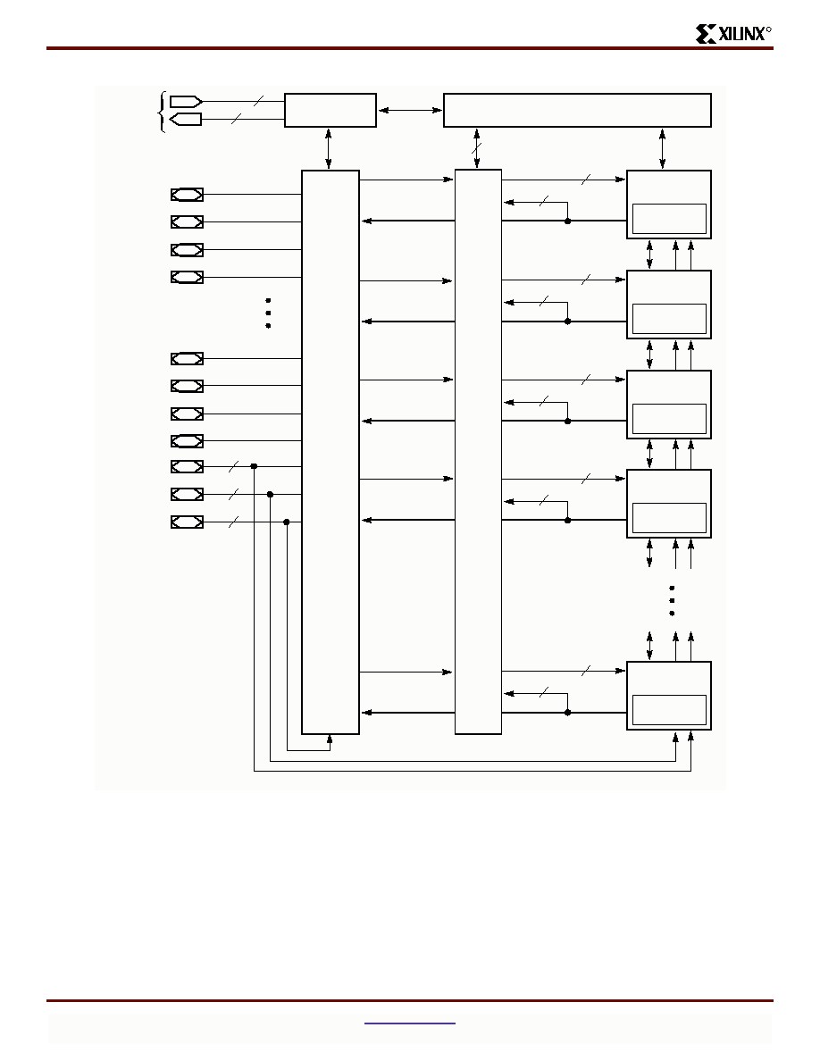
Description
The XC95288XL is a 3.3V CPLD targeted for high-perfor-
mance, low-voltage applications in leading-edge communi-
cations and computing systems. It is comprised of 16
54V18 Function Blocks, providing 6,400 usable gates with
propagation delays of 6 ns. See
Figure 2
for architecture
overview.
Power Estimation
Power dissipation in CPLDs can vary substantially depend-
ing on the system frequency, design application and output
loading. To help reduce power dissipation, each macrocell
in a XC9500XL device may be configured for low-power
mode (from the default high-performance mode). In addi-
tion, unused product-terms and macrocells are automati-
cally deactivated by the software to further conserve power.
For a general estimate of I
CC
, the following equation may be
used:
I
CC
(mA) = MC
HS
(0.175*PT
HS
+ 0.345) + MC
LP
(0.052*PT
LP
+ 0.272) + 0.04 * MC
TOG
(MC
HS
+MC
LP
)* f
where:
MC
HS
= # macrocells in high-speed configuration
PT
HS
= average number of high-speed product terms
per macrocell
MC
LP
= # macrocells in low power configuration
PT
LP
= average number of low power product terms per
macrocell
f = maximum clock frequency
MCTOG = average % of flip-flops toggling per clock
(~12%)
This calculation was derived from laboratory measurements
of an XC9500XL part filled with 16-bit counters and allowing
a single output (the LSB) to be enabled. The actual I
CC
value varies with the design application and should be veri-
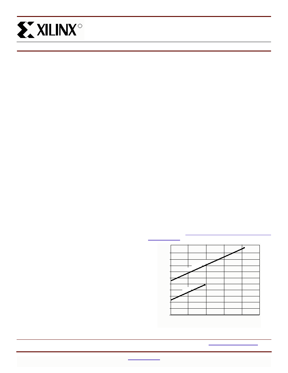
fied during normal system operation.
Figure 1
shows the
above estimation in a graphical form. For a more detailed
discussion of power consumption in this device, see Xilinx
application note
XAPP114, "Understanding XC9500XL
CPLD Power."
0
XC95288XL High Performance
CPLD
DS055 (v1.5) June 20, 2002
0
5
Product Specification
R
Figure 1: Typical I
CC
vs. Frequency for XC95288XL
Clock Frequency (MHz)
Typical I
CC
(mA)
100
200
250
DS055_01_121501
200
250
300
350
400
450
500
550
50
50
150
150
100
0
94 MHz
Hig
h P
erfo
rmanc
e
208 MHz
Lo
w P
ower
XC95288XL High Performance CPLD
2
www.xilinx.com
DS055 (v1.5) June 20, 2002
1-800-255-7778
Product Specification
R
Figure 2: XC95288XL Architecture
Function Block outputs (indicated by the bold line) drive the I/O Blocks directly.
In-System Programming Controller
JTAG
Controller
I/O
Blocks
Function
Block 1
Macrocells
1 to 18
Macrocells
1 to 18
JTAG Port
3
54
I/O/GTS
I/O/GSR
I/O/GCK
I/O
I/O
I/O
I/O
4
1
I/O
I/O
I/O
I/O
3
DS055_02_101300
1
Function
Block 2
54
18
18
Function
Block 3
Macrocells
1 to 18
Macrocells
1 to 18
54
Function
Block 16
54
18
18
Function
Block 4
Macrocells
1 to 18
54
18
Fast CONNECT II Switch Matrix
XC95288XL High Performance CPLD
DS055 (v1.5) June 20, 2002
www.xilinx.com
3
Product Specification
1-800-255-7778
R
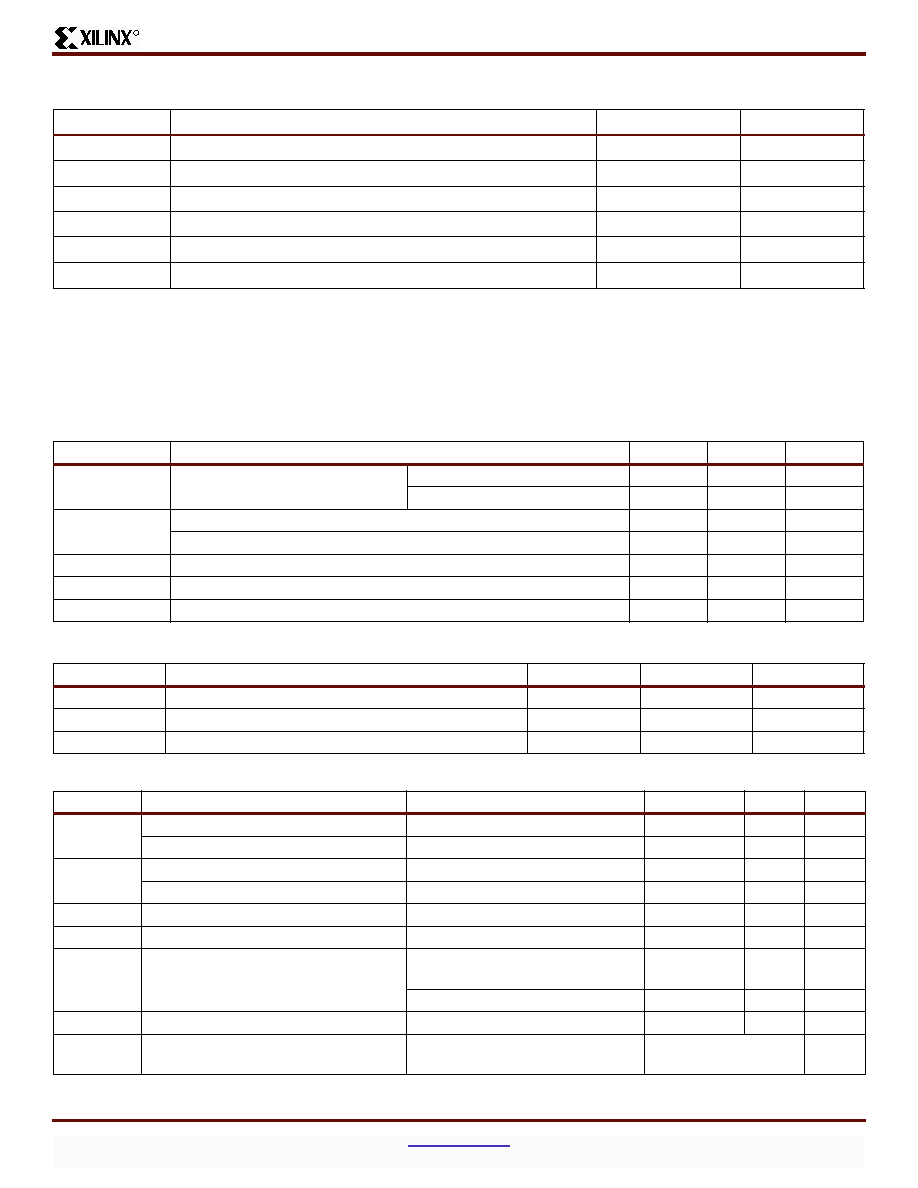
Absolute Maximum Ratings
Recommended Operation Conditions
Quality and Reliability Characteristics
DC Characteristic Over Recommended Operating Conditions
Symbol
Description
Value
Units
V
CC
Supply voltage relative to GND
≠0.5 to 4.0
V
V
IN
Input voltage relative to GND
(1)
≠0.5 to 5.5
V
V
TS
Voltage applied to 3-state output
(1)
≠0.5 to 5.5
V
T
STG
Storage temperature (ambient)
≠65 to +150
o
C
T
SOL
Maximum soldering temperature (10s @ 1/16 in. = 1.5 mm)
+260
o
C
T
J
Junction temperature
+150
o
C
Notes:
1.
Maximum DC undershoot below GND must be limited to either 0.5V or 10 mA, whichever is easier to achieve. During transitions, the
device pins may undershoot to ≠2.0 V or overshoot to +7.0V, provided this over- or undershoot lasts less than 10 ns and with the
forcing current being limited to 200 mA.
2.
Stresses beyond those listed under Absolute Maximum Ratings may cause permanent damage to the device. These are stress
ratings only, and functional operation of the device at these or any other conditions beyond those listed under Operating Conditions
is not implied. Exposure to Absolute Maximum Ratings conditions for extended periods of time may affect device reliability.
Symbol
Parameter
Min
Max
Units
V
CCINT
Supply voltage for internal logic
and input buffers
Commercial T
A
= 0
o
C to 70
o
C
3.0
3.6
V
Industrial T
A
= ≠40
o
C to +85
o
C
3.0
3.6
V
V
CCIO
Supply voltage for output drivers for 3.3V operation
3.0
3.6
V
Supply voltage for output drivers for 2.5V operation
2.3
2.7
V
V
IL
Low-level input voltage
0
0.80
V
V
IH
High-level input voltage
2.0
5.5
V
V
O
Output voltage
0
V
CCIO
V
Symbol
Parameter
Min
Max
Units
T
DR
Data Retention
20
-
Years
N
PE
Program/Erase Cycles (Endurance)
10,000
-
Cycles
V
ESD
Electrostatic Discharge (ESD)
2,000
-
Volts
Symbol
Parameter
Test Conditions
Min
Max
Units
V
OH
Output high voltage for 3.3V outputs
I
OH
= ≠4.0 mA
2.4
-
V
Output high voltage for 2.5V outputs
I
OH
= ≠500
µ
A
90% V
CCIO
-
V
V
OL
Output low voltage for 3.3V outputs
I
OL
= 8.0 mA
-
0.4
V
Output low voltage for 2.5V outputs
I
OL
= 500
µ
A
-
0.4
V
I
IL
Input leakage current
V
CC
= Max; V
IN
= GND or V
CC
-
±10
µ
A
I
IH
I/O high-Z leakage current
V
CC
= Max; V
IN
= GND or V
CC
-
±10
µ
A
I
IH
I/O high-Z leakage current
V
CC
= Max; V
CCIO
= Max;
V
IN
= GND or 3.6V
-
±10
µ
A
V
CC
Min < V
IN
< 5.5V
-
±50
µ
A
C
IN
I/O capacitance
V
IN
= GND; f = 1.0 MHz
-
10
pF
I
CC
Operating supply current
(low power mode, active)
V
IN
= GND, No load; f = 1.0 MHz
85 (Typical)
mA
XC95288XL High Performance CPLD
4
www.xilinx.com
DS055 (v1.5) June 20, 2002
1-800-255-7778
Product Specification
R
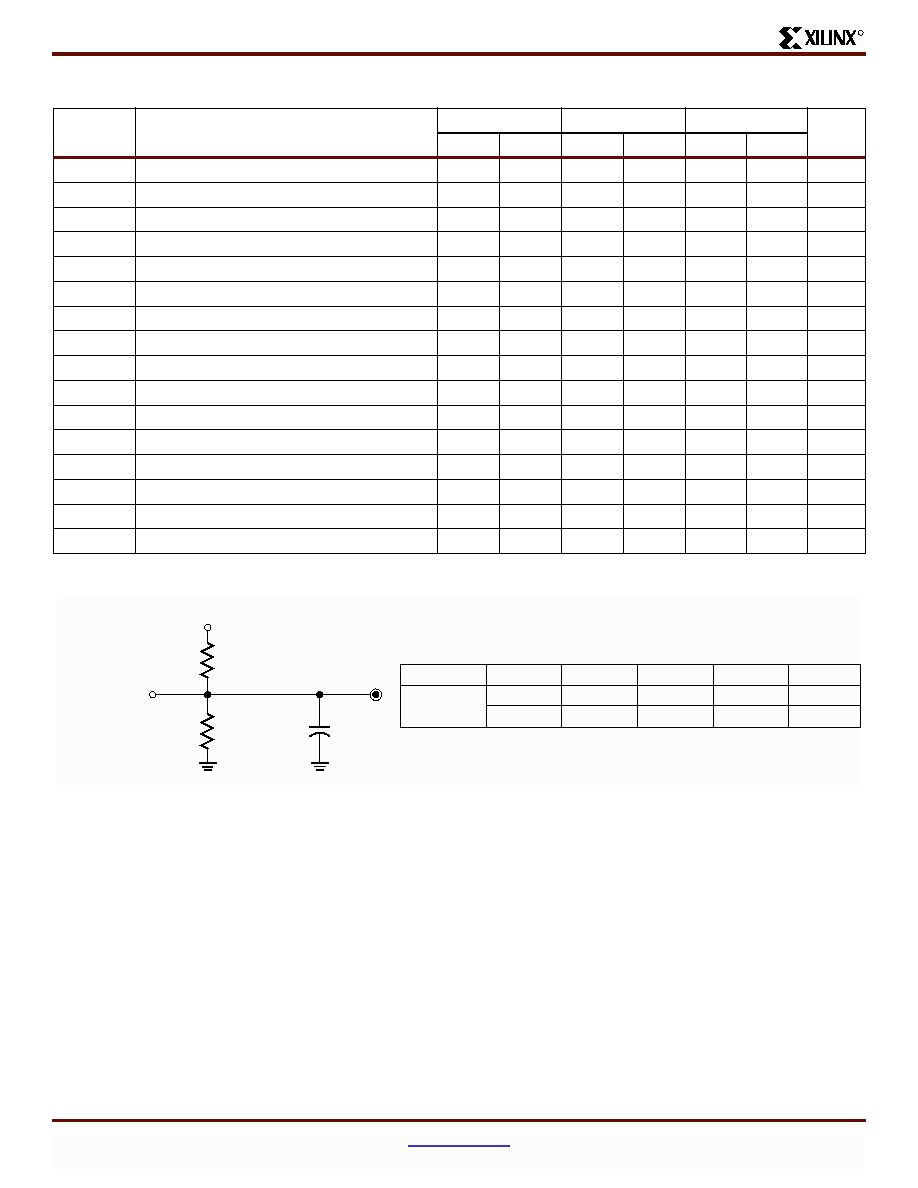
AC Characteristics
Symbol
Parameter
XC95288XL-6
XC95288XL-7
XC95288XL-10
Units
Min
Max
Min
Max
Min
Max
T
PD
I/O to output valid
-
6.0
-
7.5
-
10.0
ns
T
SU
I/O setup time before GCK
4.0
-
4.8
-
6.5
-
ns
T
H
I/O hold time after GCK
0
-
0
-
0
-
ns
T
CO
GCK to output valid
-
3.8
-
4.5
-
5.8
ns
f
SYSTEM
Multiple FB internal operating frequency
-
208.3
-
125.0
-
100.0
MHz
T
PSU
I/O setup time before p-term clock input
1.0
-
1.6
-
2.1
-
ns
T
PH
I/O hold time after p-term clock input
2.6
-
3.2
-
4.4
-
ns
T
PCO
P-term clock output valid
-
6.8
-
7.7
-
10.2
ns
T
OE
GTS to output valid
-
4.5
-
5.0
-
7.0
ns
T
OD
GTS to output disable
-
4.5
-
5.0
-
7.0
ns
T
POE
Product term OE to output enabled
-
8.4
-
9.5
-
11.0
ns
T
POD
Product term OE to output disabled
-
8.4
-
9.5
-
11.0
ns
T
AO
GSR to output valid
-
10.8
-
12.0
-
14.5
ns
T
PAO
P-term S/R to output valid
-
11.8
-
12.6
-
15.3
ns
T
WLH
GCK pulse width (High or Low)
2.4
-
4.0
-
4.5
-
ns
T
PLH
P-term clock pulse width (High or Low)
6.0
-
6.5
-
7.0
-
ns
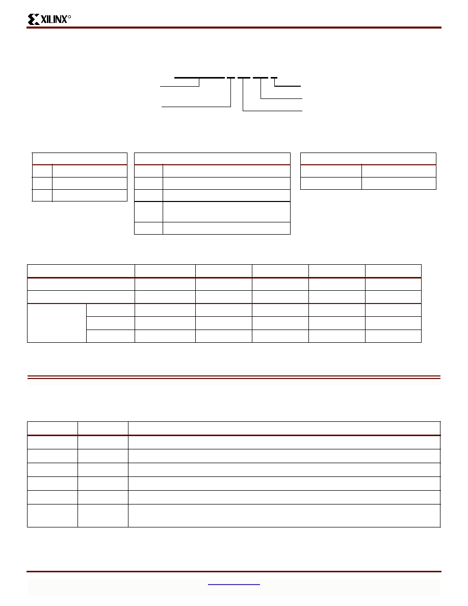
Figure 3: AC Load Circuit
Device Output
Output Type
V
TEST
3.3V
2.5V
V
TEST
R
1
320
250
R
1
R
2
C
L
R
2
360
660
C
L
35 pF
35 pF
DS058_03_081500
V
CCIO
3.3V
2.5V
XC95288XL High Performance CPLD
DS055 (v1.5) June 20, 2002
www.xilinx.com
5
Product Specification
1-800-255-7778
R
Internal Timing Parameters
Symbol
Parameter
XC95288XL-6
XC95288XL-7
XC95288XL-10
Units
Min
Max
Min
Max
Min
Max
Buffer Delays
T
IN
Input buffer delay
-
2.2
-
2.3
-
3.5
ns
T
GCK
GCK buffer delay
-
1.2
-
1.5
-
1.8
ns
T
GSR
GSR buffer delay
-
2.2
-
3.1
-
4.5
ns
T
GTS
GTS buffer delay
-
4.5
-
5.0
-
7.0
ns
T
OUT
Output buffer delay
-
2.4
-
2.5
-
3.0
ns
T
EN
Output buffer enable/disable
delay
-
0
-
0
-
0
ns
Product Term Control Delays
T
PTCK
Product term clock delay
-
2.0
-
2.4
-
2.7
ns
T
PTSR
Product term set/reset delay
-
1.0
-
1.4
-
1.8
ns
T
PTTS
Product term 3-state delay
-
6.2
-
7.2
-
7.5
ns
Internal Register and Combinatorial Delays
T
PDI
Combinatorial logic propagation delay
-
0.4
-
1.3
-
1.7
ns
T
SUI
Register setup time
2.0
-
2.6
-
3.0
-
ns
T
HI
Register hold time
1.6
-
2.2
-
3.5
-
ns
T
ECSU
Register clock enable setup time
2.0
-
2.6
-
3.0
-
ns
T
ECHO
Register clock enable hold time
1.6
-
2.2
-
3.5
-
ns
T
COI
Register clock to output valid time
-
0.2
-
0.5
-
1.0
ns
T
AOI
Register async. S/R to output delay
-
6.2
-
6.4
-
7.0
ns
T
RAI
Register async. S/R recover before clock
6.0
7.5
10.0
ns
T
LOGI
Internal logic delay
-
1.0
-
1.4
-
1.8
ns
T
LOGILP
Internal low power logic delay
-
5.5
-
6.4
-
7.3
ns
Feedback Delays
T
F
Fast CONNECT II feedback delay
-
1.6
-
3.5
-
4.2
ns
Time Adders
T
PTA
Incremental product term allocator delay
(first incremental delay)
-
0.8
-
0.8
-
1.0
ns
T
PTA2
Incremental product term allocator delay
(subsequent incremental delay)
-
0.3
-
0.3
-
0.4
ns
T
SLEW
Slew-rate limited delay
-
3.5
-
4.0
-
4.5
ns
XC95288XL High Performance CPLD
6
www.xilinx.com
DS055 (v1.5) June 20, 2002
1-800-255-7778
Product Specification
R
XC95288XL I/O Pins
Func-
tion
Block
Macro-
cell
TQ144 PQ208 BG256 FG256
CS280
BScan
Order
Func-
tion
Block
Macro-
cell
TQ144 PQ208 BG256 FG256 CS280
BScan
Order
1
1
≠
≠
≠
≠
≠
861
3
1
≠
≠
≠
≠
≠
753
1
2
≠
28
L1
H1
K2
858
3
2
28
38
P1
L2
N2
750
1
3
≠
29
L2
H5
K3
855
3
3
≠
39
R1
L5
P1
747
1
4
≠
≠
≠
≠
≠
852
3
4
≠
≠
≠
≠
≠
744
1
5
20
30
L3
J1
K4
849
3
5
≠
40
P3
M1
P2
741
1
6
21
31
L4
J5
L1
846
3
6
≠
41
R2
L4
P3
738
1
7
≠
≠
≠
≠
≠
843
3
7
≠
≠
≠
≠
≠
735
1
8
22
32
M1
J2
L2
840
3
8
≠
43
P4
N1
P4
732
1
9
≠
≠
M2
J3
L3
837
3
9
≠
≠
R3
L3
R1
729
1
10
23
33
M3
K1
L4
834
3
10
30
(1)
44
(1)
T2
(1)
M2
(1)
R3
(1)
726
1
11
≠
≠
M4
J4
M1
831
3
11
≠
≠
U1
M4
R2
723
1
12
24
34
N1
K2
M2
828
3
12
31
45
T3
P1
R4
720
1
13
≠
≠
≠
≠
≠
825
3
13
≠
≠
≠
≠
≠
717
1
14
25
35
N2
K5
M3
822
3
14
32
(1)
46
(1)
U2
(1)
M3
(1)
T1
(1)
714
1
15
26
36
N3
L1
M4
819
3
15
33
47
V1
N2
T2
711
1
16
≠
≠
≠
≠
≠
816
3
16
≠
≠
≠
≠
≠
708
1
17
27
37
N4
K3
N1
813
3
17
≠
48
T4
N4
T3
705
1
18
≠
≠
≠
≠
≠
810
3
18
≠
≠
≠
≠
≠
702
2
1
≠
≠
≠
≠
≠
807
4
1
≠
≠
≠
≠
≠
699
2
2
9
15
G2
D1
G3
804
4
2
2
(1)
3
(1)
C2
(1)
D3
(1)
C2
(1)
696
2
3
10
16
G1
G4
G2
801
4
3
≠
4
D2
D2
B1
693
2
4
≠
≠
≠
≠
≠
798
4
4
≠
≠
≠
≠
≠
690
2
5
11
17
H4
E1
G1
795
4
5
3
(1)
5
(1)
D3
(1)
E3
(1)
C1
(1)
687
2
6
12
18
H3
G3
G4
792
4
6
4
6
E4
C2
D4
684
2
7
≠
≠
≠
≠
≠
789
4
7
≠
≠
≠
≠
≠
681
2
8
13
19
H2
G2
H1
786
4
8
5
(1)
7
(1)
C1
(1)
D4
(1)
D3
(1)
678
2
9
≠
≠
H1
F5
H3
783
4
9
≠
≠
D1
B1
D2
675
2
10
14
20
J4
F1
H2
780
4
10
≠
8
E3
E4
D1
672
2
11
≠
≠
J3
G5
H4
777
4
11
≠
≠
E2
C1
E3
669
2
12
15
21
J2
H2
J1
774
4
12
6
(1)
9
(1)
E1
(1)
E5
(1)
E2
(1)
666
2
13
≠
≠
≠
≠
≠
771
4
13
≠
≠
≠
≠
≠
663
2
14
16
22
J1
H4
J2
768
4
14
7
10
F3
E2
E4
660
2
15
17
23
K2
G1
J3
765
4
15
≠
12
F2
F2
F3
657
2
16
≠
≠
≠
≠
≠
762
4
16
≠
≠
≠
≠
≠
654
2
17
19
25
K1
H3
J4
759
4
17
≠
14
G3
E6
F4
651
2
18
≠
≠
≠
≠
≠
756
4
18
≠
≠
≠
≠
≠
648
Notes:
1.
Global control pin.
XC95288XL High Performance CPLD
DS055 (v1.5) June 20, 2002
www.xilinx.com
7
Product Specification
1-800-255-7778
R
5
1
≠
≠
≠
≠
≠
645
7
1
≠
≠
≠
≠
≠
537
5
2
34
49
U3
R1
U1
642
7
2
≠
62
W6
R3
W5
534
5
3
≠
50
V2
N3
V1
639
7
3
45
63
Y6
M6
U6
531
5
4
≠
≠
≠
≠
≠
636
7
4
≠
≠
≠
≠
≠
528
5
5
35
51
V3
P2
U2
633
7
5
46
64
V7
T3
V6
525
5
6
≠
54
Y2
P4
V3
630
7
6
≠
66
U8
T4
W6
522
5
7
≠
≠
≠
≠
≠
627
7
7
≠
≠
≠
≠
≠
519
5
8
38
(1)
55
(1)
W4
(1)
P5
(1)
W2
(1)
624
7
8
≠
67
W7
P7
U7
516
5
9
≠
≠
V4
T2
W3
621
7
9
≠
≠
Y7
T5
V7
513
5
10
39
56
U5
N5
T4
618
7
10
≠
69
V8
N7
W7
510
5
11
≠
≠
Y3
R4
U4
615
7
11
≠
≠
W8
R7
T7
507
5
12
40
57
Y4
M5
V4
612
7
12
48
70
Y8
M7
W8
504
5
13
≠
≠
≠
≠
≠
609
7
13
≠
≠
≠
≠
≠
501
5
14
41
58
V5
R5
W4
606
7
14
≠
71
U9
T6
U8
498
5
15
43
60
V6
R6
V5
603
7
15
49
72
V9
N8
V8
495
5
16
≠
≠
≠
≠
≠
600
7
16
≠
≠
≠
≠
≠
492
5
17
44
61
U7
N6
T5
597
7
17
≠
73
W9
T7
T8
489
5
18
≠
≠
≠
≠
≠
594
7
18
≠
≠
≠
≠
≠
486
6
1
≠
≠
≠
≠
≠
591
8
1
-
≠
≠
≠
≠
483
6
2
135
197
D7
A5
D7
588
8
2
130
186
A9
E11
B10
480
6
3
136
198
C6
D6
A6
585
8
3
131
187
B9
A8
C10
477
6
4
≠
≠
≠
≠
≠
582
8
4
≠
≠
≠
≠
≠
474
6
5
137
199
B5
B5
B6
579
8
5
132
188
C9
C8
D10
471
6
6
138
200
A4
C6
C6
576
8
6
≠
189
D9
B8
A9
468
6
7
≠
≠
≠
≠
≠
573
8
7
≠
≠
≠
≠
≠
465
6
8
139
201
C5
A4
D6
570
8
8
133
191
A8
D8
B9
462
6
9
≠
≠
B4
E7
A5
567
8
9
≠
≠
B8
A7
C9
459
6
10
140
202
A3
A3
C5
564
8
10
134
192
C8
E9
D9
456
6
11
≠
≠
D5
C5
B5
561
8
11
≠
≠
D8
B7
A8
453
6
12
≠
203
C4
A2
D5
558
8
12
≠
193
A7
D7
B8
450
6
13
≠
≠
≠
≠
≠
555
8
13
≠
≠
≠
≠
≠
447
6
14
142
205
B2
B4
B4
552
8
14
≠
194
B7
A6
C8
444
6
15
143
(1)
206
(1)
A2
(1)
C4
(1)
C4
(1)
549
8
15
≠
195
B6
B6
B7
441
6
16
≠
≠
≠
≠
≠
546
8
16
≠
≠
≠
≠
≠
438
6
17
≠
208
C3
B3
A3
543
8
17
≠
196
A5
E8
C7
435
6
18
≠
≠
≠
≠
≠
540
8
18
≠
≠
≠
≠
≠
432
Notes:
1.
Global control pin.
XC95288XL I/O Pins (Continued)
Func-
tion
Block
Macro-
cell
TQ144 PQ208 BG256 FG256
CS280
BScan
Order
Func-
tion
Block
Macro-
cell
TQ144 PQ208 BG256 FG256 CS280
BScan
Order
XC95288XL High Performance CPLD
8
www.xilinx.com
DS055 (v1.5) June 20, 2002
1-800-255-7778
Product Specification
R
9
1
≠
≠
≠
≠
≠
429
11
1
≠
≠
≠
≠
≠
321
9
2
50
74
Y11
R8
U9
426
11
2
≠
87
Y15
P10
W13
318
9
3
51
75
W11
P8
T9
423
11
3
60
88
V14
T12
V13
315
9
4
≠
≠
≠
≠
≠
420
11
4
≠
≠
≠
≠
≠
312
9
5
52
76
V11
T8
W10
417
11
5
61
89
W15
N10
U13
309
9
6
53
77
U11
M8
V10
414
11
6
≠
90
Y16
T13
T13
306
9
7
≠
≠
≠
≠
≠
411
11
7
≠
≠
≠
≠
≠
303
9
8
54
78
Y12
T9
U10
408
11
8
≠
91
U14
M11
W14
300
9
9
≠
≠
W12
P9
W11
405
11
9
≠
≠
Y17
N11
T14
297
9
10
≠
80
V12
R9
V11
402
11
10
64
95
V16
T14
W15
294
9
11
56
82
U12
M9
U11
399
11
11
66
97
Y18
R12
V15
291
9
12
57
83
Y13
T10
T11
396
11
12
68
99
V17
T15
W16
288
9
13
≠
≠
≠
≠
≠
393
11
13
≠
≠
≠
≠
≠
285
9
14
58
84
W13
M10
W12
390
11
14
69
100
Y19
R14
U16
282
9
15
≠
85
V13
R10
V12
387
11
15
≠
101
V18
N13
W17
279
9
16
≠
≠
≠
≠
≠
384
11
16
≠
≠
≠
≠
≠
276
9
17
59
86
W14
T11
T12
381
11
17
70
102
W19
R13
W18
273
9
18
≠
≠
≠
≠
≠
378
11
18
≠
≠
≠
≠
≠
270
10
1
≠
≠
≠
≠
≠
375
12
1
≠
≠
≠
≠
≠
267
10
2
117
170
A14
B11
C14
372
12
2
110
158
B18
B13
B19
264
10
3
118
171
C13
D11
B14
369
12
3
111
159
C17
B14
B18
261
10
4
≠
≠
≠
≠
≠
366
12
4
≠
≠
≠
≠
≠
258
10
5
119
173
B13
A11
A14
363
12
5
112
160
D16
C13
B17
255
10
6
120
174
A13
D10
C13
360
12
6
≠
161
A18
A15
A18
252
10
7
≠
≠
≠
≠
≠
357
12
7
≠
≠
≠
≠
≠
249
10
8
121
175
D12
B10
B13
354
12
8
113
162
A17
C12
A17
246
10
9
≠
≠
C12
E12
A13
351
12
9
≠
≠
C16
B12
D16
243
10
10
124
178
A12
F12
A12
348
12
10
115
164
A16
D13
C16
240
10
11
125
179
B11
B9
C12
345
12
11
≠
165
C15
A14
B16
237
10
12
126
180
C11
C9
B12
342
12
12
116
166
D14
E13
A16
234
10
13
≠
≠
≠
≠
≠
339
12
13
≠
≠
≠
≠
≠
231
10
14
128
182
B10
A9
B11
336
12
14
≠
167
B15
A13
C15
228
10
15
≠
183
C10
D9
C11
333
12
15
≠
168
A15
C11
B15
225
10
16
≠
≠
≠
≠
≠
330
12
16
≠
≠
≠
≠
≠
222
10
17
129
185
D10
E10
A10
327
12
17
≠
169
C14
A12
D15
219
10
18
≠
≠
≠
≠
≠
324
12
18
≠
≠
≠
≠
≠
216
XC95288XL I/O Pins (Continued)
Func-
tion
Block
Macro-
cell
TQ144 PQ208 BG256 FG256
CS280
BScan
Order
Func-
tion
Block
Macro-
cell
TQ144 PQ208 BG256 FG256 CS280
BScan
Order

XC95288XL High Performance CPLD
DS055 (v1.5) June 20, 2002
www.xilinx.com
9
Product Specification
1-800-255-7778
R
13
1
≠
≠
≠
≠
≠
213
15
1
≠
≠
≠
≠
≠
105
13
2
71
103
Y20
P13
V17
210
15
2
79
117
P19
M12
P16
102
13
3
≠
106
V19
P15
U18
207
15
3
80
118
P20
M16
P19
99
13
4
≠
≠
≠
≠
≠
204
15
4
≠
≠
≠
≠
≠
96
13
5
≠
107
U19
N14
V19
201
15
5
≠
119
N17
K14
N17
93
13
6
≠
109
T17
R16
U19
198
15
6
≠
120
N18
L16
N18
90
13
7
≠
≠
≠
≠
≠
195
15
7
≠
≠
≠
≠
≠
87
13
8
74
110
V20
N15
T16
192
15
8
81
121
N19
K13
N19
84
13
9
≠
≠
U20
M15
T17
189
15
9
≠
≠
N20
K15
N16
81
13
10
≠
111
T18
M13
T18
186
15
10
82
122
M17
L12
M19
78
13
11
75
112
T19
P16
T19
183
15
11
83
123
M18
K16
M17
75
13
12
≠
113
R18
N16
R18
180
15
12
85
125
M20
J14
M16
72
13
13
≠
≠
≠
≠
≠
177
15
13
≠
≠
≠
≠
≠
69
13
14
76
114
P17
M14
R16
174
15
14
86
126
L19
J15
L19
66
13
15
77
115
R20
L15
R19
171
15
15
87
127
L18
J13
L18
63
13
16
≠
≠
≠
≠
≠
168
15
16
≠
≠
≠
≠
≠
60
13
17
78
116
P18
L13
P17
165
15
17
88
128
L20
J16
L17
57
13
18
≠
≠
≠
≠
≠
162
15
18
≠
≠
≠
≠
≠
54
14
1
≠
≠
≠
≠
≠
159
16
1
≠
≠
≠
≠
≠
51
14
2
≠
144
G19
F15
G19
156
16
2
91
131
K19
K12
L16
48
14
3
100
145
F19
E15
G16
153
16
3
92
133
K18
J12
K18
45
14
4
≠
≠
≠
≠
≠
150
16
4
≠
≠
≠
≠
≠
42
14
5
101
146
E20
F13
F19
147
16
5
93
134
K17
H15
K17
39
14
6
102
147
G17
D16
F18
144
16
6
94
135
J20
H14
K16
36
14
7
≠
≠
≠
≠
≠
141
16
7
≠
≠
≠
≠
≠
33
14
8
103
148
F18
F14
F17
138
16
8
95
136
J19
G16
J19
30
14
9
≠
≠
E19
C16
F16
135
16
9
≠
≠
J18
H13
J18
27
14
10
104
149
D20
E14
E19
132
16
10
96
137
J17
G15
J17
24
14
11
105
150
E18
D15
E17
129
16
11
97
138
H20
H16
J16
21
14
12
≠
151
D19
G12
E18
126
16
12
98
139
H19
F16
H19
18
14
13
≠
≠
≠
≠
≠
123
16
13
≠
≠
≠
≠
≠
15
14
14
106
152
C20
C15
E16
120
16
14
≠
140
H18
H12
H18
12
14
15
107
154
D18
D14
D18
117
16
15
≠
142
H17
E16
H17
9
14
16
≠
≠
≠
≠
≠
114
16
16
≠
≠
≠
≠
≠
6
14
17
≠
155
C18
B16
D17
111
16
17
≠
143
G20
G14
H16
3
14
18
≠
≠
≠
≠
≠
108
16
18
≠
≠
≠
≠
≠
0
XC95288XL I/O Pins (Continued)
Func-
tion
Block
Macro-
cell
TQ144 PQ208 BG256 FG256
CS280
BScan
Order
Func-
tion
Block
Macro-
cell
TQ144 PQ208 BG256 FG256 CS280
BScan
Order
XC95288XL High Performance CPLD
10
www.xilinx.com
DS055 (v1.5) June 20, 2002
1-800-255-7778
Product Specification
R
XC95288XL Global, JTAG and Power Pins
Pin Type
TQ144
PQ208
BG256
FG256
CS280
I/O/GCK1
30
44
T2
M2
R3
I/O/GCK2
32
46
U2
M3
T1
I/O/GCK3
38
55
W4
P5
W2
I/O/GTS1
5
7
C1
D4
D3
I/O/GTS2
6
9
E1
E5
E2
I/O/GTS3
2
3
C2
D3
C2
I/O/GTS4
3
5
D3
E3
C1
I/O/GSR
143
206
A2
C4
C4
TCK
67
98
U16
P12
T15
TDI
63
94
W16
R11
U14
TDO
122
176
B12
A10
D13
TMS
65
96
W17
N12
U15
V
CCINT
3.3V
8, 42, 84, 141
11, 59, 124, 153,
204
F1, P2, W5, Y9,
V10, U13, W18,
T20, M19, F20, E17,
B17, B14, A10, C7,
B3, G4
F4, F7, G6, H6, J6,
K6, L7, F8, L8, F9,
L9, F10, L10, G11,
H11, J11, K11
E1, F2, N3, U5, W9,
V9, U12, V16, R17,
M18, G18, D19,
C18, A15, A11, D8,
A4
V
CCIO
2.5V/3.3 V 1, 37, 55, 73, 109,
127
1, 26, 53, 65, 79,
92, 105, 132, 157,
172, 181, 184
D4, D6, D11, D15,
D17, F4, F17, K4,
L17, R4, R17, U4,
U6, U10, U15, U17
F3, K4, D5, F6, L6,
P6, C7, N9, C10,
F11, L11, P11, D12,
G13, L14
C3, F1, K1, N4, V2
T6, T10, V14, V18,
P18, K19, G17,
C19, D14, D12, D11,
A7
GND
18, 29, 36, 47, 62,
72, 89, 90, 99,
108, 114, 123,
144
2, 13, 24, 27, 42,
52, 68, 81, 93,
104,1 08, 129,
130, 141, 156,
163, 177, 190,
207
B1, K3, T1, Y5,
W10, Y10, Y14,
V15, U18, R19, K20,
G18, B16, D13, A11,
A6, J9, J10, J11,
J12, K9, K10, K11,
K12, L9, L10, L11,
L12, M9, M10, M11,
M12
A1, A16, C14, T1,
B2, B15, R2, C3,
P3, G7, H7, J7, K7,
G8, H8, J8, K8, G9,
H9, J9, K9, G10,
H10, J10, K10, P14,
R15, T16
E5, F5, G5, H5, J5,
K5, L5, M5, N5, R5,
R6, R7, R8, R9 R10,
R11, R12, R13, R14,
R15, P15, N15,
M15, L15, K15, J15,
H15, G15, F15, E15,
E14, E13, E12, E11,
E10, E9, E8, E7, E6,
P5
No Connects
≠
≠
A1, A19, A20, B19,
B20, C19, W1, W2,
W3, W20, Y1
-
A1, B2, W1, U3,
W19, U17, A19,
C17, A2, B3
XC95288XL High Performance CPLD
DS055 (v1.5) June 20, 2002
www.xilinx.com
11
Product Specification
1-800-255-7778
R
Ordering Information
Component Availability
Revision History
The following table shows the revision history for this document.
XC95288XL -6 TQ 144 C
Example:
Temperature Range
Number of Pins
Package Type
Device Type
Speed Grade
Device Ordering Options
Speed
Package
Temperature
-10
10 ns pin-to-pin delay
TQ144
144-pin Thin Quad Flat Pack (TQFP)
C = Commercial
T
A
= 0∞C to +70∞C
-7
7.5 ns pin-to-pin delay
PQ208
208-pin Plastic Quad Flat Pack (PQFP)
I = Industrial
T
A
= ≠40∞C to +85∞C
-6
6 ns pin-to-pin delay
BG256
256-pin Plastic Ball Grid Array (BGA)
FG256
256-pin Plastic Fine-Pitch Ball Grid
Array (FBGA)
CS280
280-pin Chip Scale Package (CSP)
Pins
144
208
256
256
280
Type
Plastic TQFP
Plastic PQFP
Plastic BGA
Plastic FBGA
Plastic CSP
Code
TQ44
PQ208
BG256
FG256
CS280
XC95288XL
-10
C, I
C, I
C, I
C, I
C, I
-7
C, I
C, I
C, I
C, I
C, I
-6
C
C
C
C
C
Notes:
1.
C = Commercial (T
A
= 0
o
C to +70
o
C); I = Industrial (T
A
= ≠40
o
C to +85
o
C).
Date
Version
Revision
09/28/98
1.0
Initial Xilinx release.
02/05/99
1.1
Updateed pinouts to reflect BG256 (replaces BG352).
06/07/99
1.2
Added -7 speed and CS280 package.
02/08/01
1.3
Updated -6 AC and timing parameters, added FG256 package.
03/19/01
1.4
Pinout corrections.
06/20/02
1.5
Updated I
CC
equation, page 1. Updated Component Availability Chart: added -7 Industrial.
Added additional I
IH
test conditions and measurements to DC Characteristics table.