December 4, 1998 (Version 5.0) 1
9
Features
∑ 5 ns pin-to-pin logic delays on all pins
∑
f
CNT
to 100 MHz
∑ 36 macrocells with 800 usable gates
∑ Up to 34 user I/O pins
∑ 5 V in-system programmable (ISP)
- Endurance of 10,000 program/erase cycles
- Program/erase over full commercial voltage and
temperature range
∑ Enhanced pin-locking architecture
∑ Flexible 36V18 Function Block
- 90 product terms drive any or all of 18 macrocells
within Function Block
- Global and product term clocks, output enables, set
and reset signals
∑ Extensive IEEE Std 1149.1 boundary-scan (JTAG)
support
∑ Programmable power reduction mode in each
macrocell
∑ Slew rate control on individual outputs
∑ User programmable ground pin capability
∑ Extended pattern security features for design protection
∑ High-drive 24 mA outputs
∑ 3.3 V or 5 V I/O capability
∑ Advanced CMOS 5V FastFLASH technology
∑ Supports parallel programming of more than one
XC9500 concurrently
∑ Available in 44-pin PLCC, 44-pin VQFP, and 48-pin
CSP packages
Description
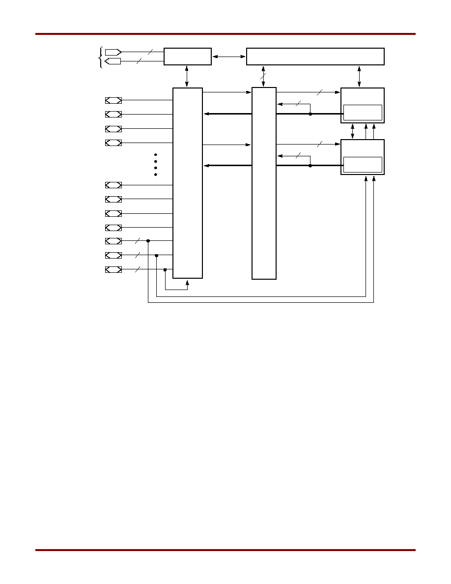
The XC9536 is a high-performance CPLD providing
advanced in-system programming and test capabilities for
general purpose logic integration. It is comprised of two
36V18 Function Blocks, providing 800 usable gates with
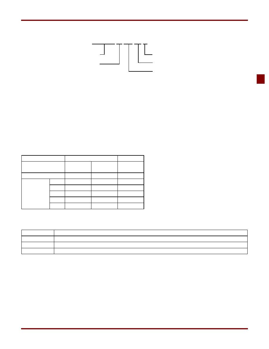
propagation delays of 5 ns. See
Figure 2
for the architec-
ture overview.
Power Management
Power dissipation can be reduced in the XC9536 by config-
uring macrocells to standard or low-power modes of opera-
tion. Unused macrocells are turned off to minimize power
dissipation.
Operating current for each design can be approximated for
specific operating conditions using the following equation:
I
CC
(mA) =
MC
HP
(1.7) + MC
LP
(0.9) + MC (0.006 mA/MHz) f
Where:
MC
HP
= Macrocells in high-performance mode
MC
LP
= Macrocells in low-power mode
MC = Total number of macrocells used
f = Clock frequency (MHz)
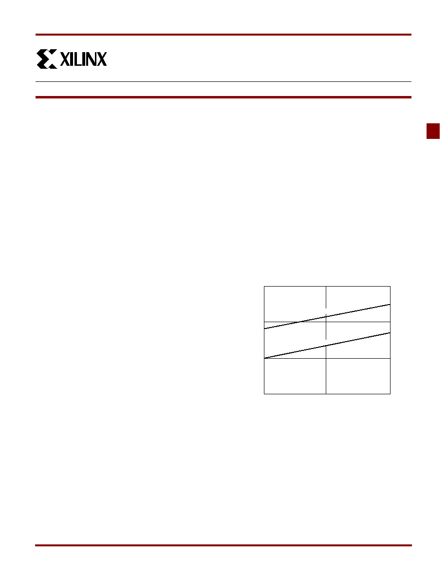
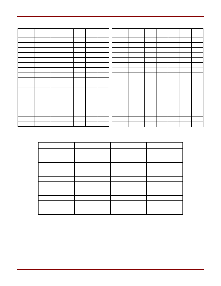
Figure 1
shows a typical calculation for the XC9536 device.
1
XC9536 In-System Programmable
CPLD
December 4, 1998 (Version 5.0)
1
1*
Product Specification
Æ
Clock Frequency (MHz)
Typical I
CC
(mA)
0
50
(50)
(30)
(83)
(50)
100
High Performance
Low Power
X5920
Figure 1: Typical I
CC
vs. Frequency For XC9536
XC9536 In-System Programmable CPLD
2 December 4, 1998 (Version 5.0)
In-System Programming Controller
JTAG
Controller
I/O
Blocks
Function
Block 1
Macrocells
1 to 18
Macrocells
1 to 18
JTAG Port
3
36
I/O/GTS
I/O/GSR
I/O/GCK
I/O
I/O
I/O
I/O
2
1
I/O
I/O
I/O
I/O
3
X5919
1
Function
Block 2
36
18
18
FastCONNECT Switch Matrix
Figure 2: XC9536 Architecture
Note:
Function Block outputs (indicated by the bold line) drive the I/O Blocks directly

December 4, 1998 (Version 5.0) 3
XC9536 In-System Programmable CPLD
Absolute Maximum Ratings
Warning: Stresses beyond those listed under Absolute Maximum Ratings may cause permanent damage to the device. These are
stress ratings only, and functional operation of the device at these or any other conditions beyond those listed under
Recommended Operating Conditions is not implied. Exposure to Absolute Maximum Rating conditions for extended periods
of time may affect device reliability.
Recommended Operating Conditions
1
Note 1. Numbers in parenthesis are for industrial-temperature range versions.
Endurance Characteristics
Symbol Parameter Value Units
V
CC
Supply voltage relative to GND -0.5 to 7.0 V
V
IN
DC input voltage relative to GND -0.5 to V
CC
+ 0.5 V
V
TS
Voltage applied to 3-state output with respect to GND -0.5 to V
CC
+ 0.5 V
T
STG
Storage temperature -65 to +150
∞
C
T
SOL
Max soldering temperature (10 s @ 1/16 in = 1.5 mm) +260
∞
C
Symbol Parameter Min Max Units
V
CCINT
Supply voltage for internal logic and input buffer 4.75
(4.5)
5.25
(5.5)
V
V
CCIO
Supply voltage for output drivers for 5 V operation 4.75 (4.5) 5.25 (5.5) V
Supply voltage for output drivers for 3.3 V operation 3.0 3.6 V
V
IL
Low-level input voltage 0 0.80 V
V
IH
High-level input voltage 2.0 V
CCINT
+0.5 V
V
O
Output voltage 0 V
CCIO
V
Symbol Parameter Min Max Units
t
DR
Data Retention 20 - Years
N
PE
Program/Erase Cycles 10,000 - Cycles
XC9536 In-System Programmable CPLD
4 December 4, 1998 (Version 5.0)
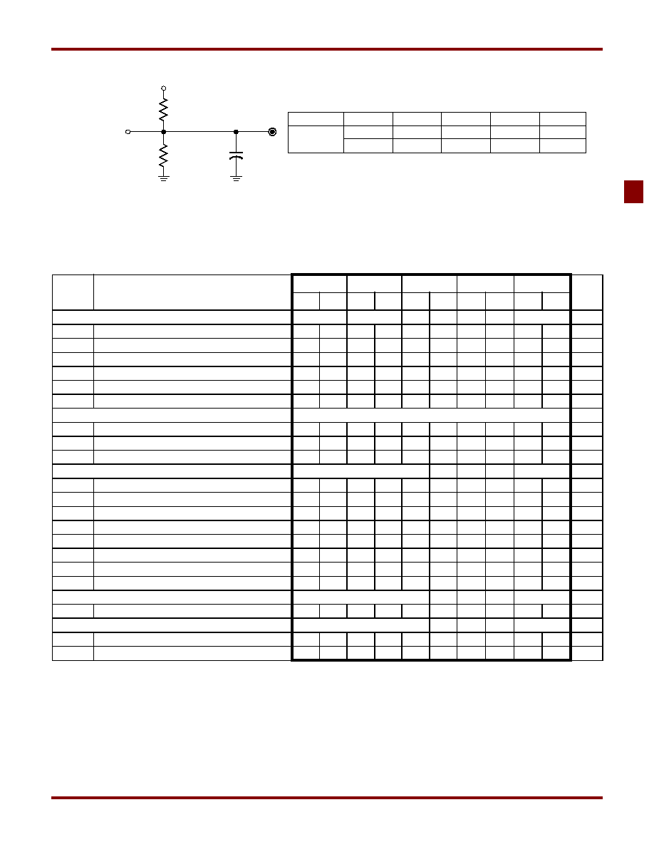
DC Characteristics Over Recommended Operating Conditions
AC Characteristics
Note:
1. f
CNT
is the fastest 16-bit counter frequency available.
f
CNT
is also the Export Control Maximum flip-flop toggle rate, f
TOG
.
2. f
SYSTEM
is the internal operating frequency for general purpose system designs spanning multiple FBs.
Symbol Parameter Test Conditions Min Max Units
V
OH
Output high voltage for 5 V operation I
OH
= -4.0 mA
V
CC
= Min
2.4 V
Output high voltage for 3.3 V operation I
OH
= -3.2 mA
V
CC
= Min
2.4 V
V
OL
Output low voltage for 5 V operation I
OL
= 24 mA
V
CC
= Min
0.5 V
Output low voltage for 3.3 V operation I
OL
= 10 mA
V
CC
= Min
0.4 V
I
IL
Input leakage current V
CC
= Max
V
IN
= GND or V
CC
±
10.0
µ
A
I
IH
I/O high-Z leakage current V
CC
= Max
V
IN
= GND or V
CC
±
10.0
µ
A
C
IN
I/O capacitance
V
IN
= GND
f = 1.0 MHz
10.0 pF
I
CC
Operating Supply Current
(low power mode, active)
V
I
= GND, No load
f = 1.0 MHz
30 (Typ)
mA
Symbol Parameter
XC9536-5 XC9536-6 XC9536-7 XC9536-10 XC9536-15
Units
Min
Max
Min
Max Min Max Min
Max
Min
Max
t
PD
I/O to output valid 5.0 6.0 7.5 10.0 15.0 ns
t
SU
I/O setup time before GCK 3.5 3.5 4.5 6.0 8.0 ns
t
H
I/O hold time after GCK 0.0 0.0 0.0 0.0 0.0 ns
t
CO
GCK to output valid 4.0 4.0 4.5 6.0 8.0 ns
f
CNT
1
16-bit counter frequency 100.0 100.0 83.3 66.7 55.6 MHz
f
SYSTEM
2
Multiple FB internal operating frequency 100.0 100.0 83.3 66.7 55.6 MHz
t
PSU
I/O setup time before p-term clock input 0.5 0.5 0.5 2.0 4.0 ns
t
PH
I/O hold time after p-term clock input 3.0 3.0 4.0 4.0 4.0 ns
t
PCO
P-term clock to output valid 7.0 7.0 8.5 10.0 12.0 ns
t
OE
GTS to output valid 5.0 5.0 5.5 6.0 11.0 ns
t
OD
GTS to output disable 5.0 5.0 5.5 6.0 11.0 ns
t
POE
Product term OE to output enabled 9.0 9.0 9.5 10.0 14.0 ns
t
POD
Product term OE to output disabled 9.0 9.0 9.5 10.0 14.0 ns
t
WLH
GCK pulse width (High or Low) 4.0 4.0 4.0 4.5 5.5 ns
December 4, 1998 (Version 5.0) 5
XC9536 In-System Programmable CPLD
Internal Timing Parameters
Note:
3. t
PTA
is multiplied by the span of the function as defined in the family data sheet.
Symbol Parameter
XC9536-5 XC9536-6 XC9536-7 XC9536-10 XC9536-15
Units
Min Max Min Max Min Max Min
Max
Min
Max
Buffer Delays
t
IN
Input buffer delay 1.5 1.5 2.5 3.5 4.5 ns
t
GCK
GCK buffer delay 1.5 1.5 1.5 2.5 3.0 ns
t
GSR
GSR buffer delay 4.0 4.0 4.5 6.0 7.5 ns
t
GTS
GTS buffer delay 5.0 5.0 5.5 6.0 11.0 ns
t
OUT
Output buffer delay 2.0 2.0 2.5 3.0 4.5 ns
t
EN
Output buffer enable/disable delay 0.0 0.0 0.0 0.0 0.0 ns
Product Term Control Delays
t
PTCK
Product term clock delay 3.0 3.0 3.0 3.0 2.5 ns
t
PTSR
Product term set/reset delay 1.0 1.0 2.0 2.5 3.0 ns
t
PTTS
Product term 3-state delay 5.5 5.5 4.5 3.5 5.0 ns
Internal Register and Combinatorial delays
t
PDI
Combinatorial logic propagation delay 0.5 1.5 0.5 1.0 3.0 ns
t
SUI
Register setup time 2.5 2.5 1.5 2.5 3.5 ns
t
HI
Register hold time 1.0 1.0 3.0 3.5 4.5 ns
t
COI
Register clock to output valid time 0.5 0.5 0.5 0.5 0.5 ns
t
AOI
Register async. S/R to output delay 6.0 6.0 6.5 7.0 8.0 ns
t
RAI
Register async. S/R recovery before clock 5.0 5.0 7.5 10.0 10.0 ns
t
LOGI
Internal logic delay 1.0 1.0 2.0 2.5 3.0 ns
t
LOGILP
Internal low power logic delay 9.0 9.0 10.0 11.0 11.5 ns
Feedback Delays
t
F
FastCONNECT matrix feeback delay 6.0 6.0 8.0 9.5 11.0 ns
Time Adders
t
PTA
3
Incremental Product Term Allocator delay 0.8 0.8 1.0 1.0 1.0 ns
t
SLEW
Slew-rate limited delay 3.5 3.5 4.0 4.5 5.0 ns
R
1
V
TEST
C
L
R
2
Device Output
Output Type V
TEST
5.0 V
3.3 V
R
1
160
260
R
2
120
360
C
L
35 pF
35 pF
X5906
V
CCIO
5.0 V
3.3 V
Figure 3: AC Load Circuit
XC9536 In-System Programmable CPLD
6 December 4, 1998 (Version 5.0)
XC9536 I/O Pins
XC9536 Global, JTAG and Power Pins
Function
Block
Macrocell
PC44
VQ44 CS48
BScan
Order
Notes
Function
Block
Macrocell
PC44
VQ44 CS48
BScan
Order
Notes
1
1
2
40
D6
105
2
1
1
39
D7
51
1
2
3
41 C7 102 2 2 44 38 E5 48
1
3
5
43
B7
99
[1]
2
3
42
36
E6
45
[1]
1
4
4
42 C6 96 2 4 43 37 E7 42
1
5
6
44
B6
93
[1]
2
5
40
34
F6
39
[1]
1
6
8
2
A6
90
2
6
39
33
G7
36
[1]
1
7
7
1 A7 87 [1] 2 7 38 32 G6 33
1
8
9
3
C5
84
2
8
37
31
F5
30
1
9
11
5
B5
81
2
9
36
30
G5
27
1
10
12
6 A4 78 2 10 35 29 F4 24
1
11
13
7 B4 75 2 11 34 28 G4 21
1
12
14
8 A3 72 2 12 33 27 E3 18
1
13
18
12 B2 69 2 13 29 23 F2 15
1
14
19
13 B1 66 2 14 28 22 G1 12
1
15
20
14 C2 63 2 15 27 21 F1 9
1
16
22
16 C3 60 2 16 26 20 E2 6
1
17
24
18 D2 57 2 17 25 19 E1 3
1
18
≠
≠
-
54
2
18
-
-
-
0
Note: [1] Global control pin Note: [1] Global control pin
Pin Type PC44 VQ44 CS48
I/O/GCK1 5 43 B7
I/O/GCK2 6 44 B6
I/O/GCK3 7 1 A7
I/O/GTS1 42 36 E6
I/O/GTS2 40 34 F6
I/O/GSR 39 33 G7
TCK 17 11 A1
TDI 15 9 B3
TDO 30 24 G2
TMS 16 10 A2
V
CCINT
5 V 21,41 15,35 C1,F7
V
CCIO
3.3 V/5 V 32 26 G3
GND 23,10,31 17,4,25 A5, D1, F3
No Connects -- -- C4, D3, D4, E4
December 4, 1998 (Version 5.0) 7
XC9536 In-System Programmable CPLD
Ordering Information
Component Availability
C = Commercial (0
∞
C to +70
∞
C), I = Industrial (≠40
∞
C to +85
∞
C)
Revision Control
Speed Options
-15 15 ns pin-to-pin delay
-10 10 ns pin-to-pin delay
-7 7.5 ns pin-to-pin delay
-6 6 ns pin-to-pin delay
-5 5 ns pin-to-pin delay
Packaging Options
PC44 44-Pin Plastic Leaded Chip Carrier (PLCC)
VQ44 44-Pin Thin Quad Pack (VQFP)
CS48 48-Pin Chip Scale Package (CSP)
Temperature Options
C = Commercial (0
∞
C to +70
∞
C)
I = Industrial (≠40
∞
C to +85
∞
C)
XC9536 -5 PC 44 C
Device Type
Speed
Package Type
Number of Pins
Temperature Range
Pins 44 48
Type
Plastic
PLCC
Plastic
VQFP
Plastic
CSP
Code PC44 VQ44 CS48
XC9536
≠15 C,I C,I -
≠10 C,I C,I C
≠7 C,I C,I C
≠6 C C -
≠5
C
C
C
Date Reason
6/3/98 Revise datasheet to reflect new CSP package pinouts & ordering code.
11/2/98 Revise datasheet to reflect new AC characteristics and Internal Timing Parameters.
12/04/98 Revise datasheet to remove PCI compliancy statement and remove t
LF
.