
R
XC9536XL High Performance
CPLD
DS058 (v1.2) June 25, 2001
Preliminary Product Specification
Features
∑
5 ns pin-to-pin logic delays
∑
System frequency up to 178 MHz
∑
36 macrocells with 800 usable gates
∑
Available in small footprint packages
-
44-pin PLCC (34 user I/O pins)
-
44-pin VQFP (34 user I/O pins)
-
48-pin CSP (36 user I/O pins)
-
64-pin VQFP (36 user I/O pins)
∑
Optimized for high-performance 3.3V systems
-
Low power operation
-
5V tolerant I/O pins accept 5 V, 3.3V, and 2.5V
signals
-
3.3V or 2.5V output capability
-
Advanced 0.35 micron feature size CMOS
FastFLASHTM technology
∑
Advanced system features
-
In-system programmable
-
Superior pin-locking and routability with
FastCONNECT IITM switch matrix
-
Extra wide 54-input Function Blocks
-
Up to 90 product-terms per macrocell with
individual product-term allocation
-
Local clock inversion with three global and one
product-term clocks
-
Individual output enable per output pin
-
Input hysteresis on all user and boundary-scan pin
inputs
-
Bus-hold circuitry on all user pin inputs
-
Full IEEE Standard 1149.1 boundary-scan (JTAG)
∑
Fast concurrent programming
∑
Slew rate control on individual outputs
∑
Enhanced data security features
∑
Excellent quality and reliability
-
Endurance exceeding 10,000 program/erase
cycles
-
20 year data retention
-
ESD protection exceeding 2,000V
∑
Pin-compatible with 5V-core XC9536 device in the
44-pin PLCC package and the 48-pin CSP package
Description
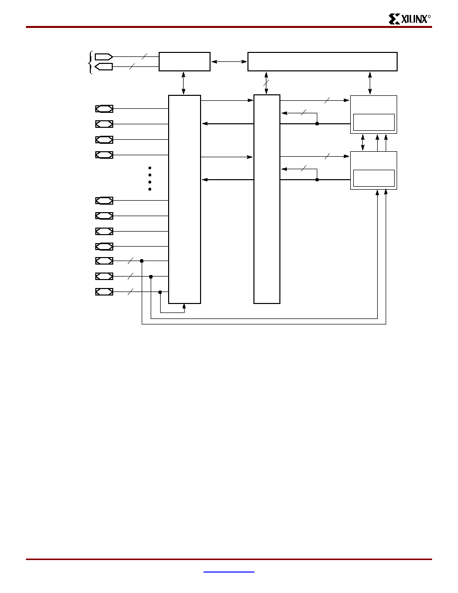
The XC9536XL is a 3.3V CPLD targeted for high-perfor
mance, low-voltage applications in leading-edge communi
cations and computing systems. It is comprised of two
54V18 Function Blocks, providing 800 usable gates with
propagation delays of 5 ns. See
Figure 2
for architecture
overview.
Power Estimation
Power dissipation in CPLDs can vary substantially depend
ing on the system frequency, design application and output
loading. To help reduce power dissipation, each macrocell
in a XC9500XL device may be configured for low-power
mode (from the default high-performance mode). In addi
tion, unused product-terms and macrocells are automati
cally deactivated by the software to further conserve power.
For a general estimate of I
CC
, the following equation may be
used:
I
CC
(mA) = MC
HP
(0.5) + MC
LP
(0.3) + MC(0.0045 mA/MHz) f
Where:
MC
HP
= Macrocells in high-performance (default) mode
MC
LP
= Macrocells in low-power mode
MC = Total number of macrocells used
f = Clock frequency (MHz)
This calculation is based on typical operating conditions
using a pattern of 16-bit up/down counters in each Function
Block with no output loading. The actual I
CC
value varies
with the design application and should be verified during
normal system operation.
Figure 1
shows the above estimation in a graphical form.
60
50
40
30
20
10
178 MHz
125 MHz
High
Perfo
rm
anc
e
Low
Po
we
r
0
50
100
150
200
250
Clock Frequency (MHz)
DS058_01_061101
Figure 1: Typical I
CC
vs. Frequency for XC9536XL
Typical I
CC
(mA)
© 2000 Xilinx, Inc. All rights reserved. All Xilinx trademarks, registered trademarks, patents, and disclaimers are as listed at
http://www.xilinx.com/legal.htm
.
All other trademarks and registered trademarks are the property of their respective owners. All specifications are subject to change without notice.
DS058 (v1.2) June 25, 2001
www.xilinx.com
1
Preliminary Product Specification
1-800-255-7778
XC9536XL High Performance CPLD
R
JTAG Port
In-System Programming Controller
JTAG
Controller
3
1
I/O
I/O
I/O
I/O
I/O
I/O
I/O
I/O
I/O/GCK
I/O/GSR
I/O/GTS
I/O
Blocks
Function
Block 1
Macrocells
1 to 18
Macrocells
1 to 18
54
2
1
3
Function
Block 2
54
18
18
FastCONNECT II Switch Matrix
DS058_02_081500
Figure 2: XC9536XL Architecture
Function Block outputs (indicated by the bold line) drive the I/O Blocks directly.
2
www.xilinx.com
DS058 (v1.2) June 25, 2001
1-800-255-7778
Preliminary Product Specification
R
XC9536XL High Performance CPLD
Absolute Maximum Ratings
Symbol
Description
Value
Units
V
CC
Supply voltage relative to GND
≠0.5 to 4.0
V
V
IN
Input voltage relative to GND
(1)
≠0.5 to 5.5
V
V
TS
Voltage applied to 3-state output
(1)
≠0.5 to 5.5
V
T
STG
Storage temperature (ambient)
≠65 to +150
o
C
T
SOL
Maximum soldering temperature (10s @ 1/16 in. = 1.5 mm)
+260
o
C
T
J
Junction temperature
+150
o
C
Notes:
1. Maximum DC undershoot below GND must be limited to either 0.5V or 10 mA, whichever is easier to achieve. During transitions, the
device pins may undershoot to ≠2.0 V or overshoot to +7.0V, provided this over- or undershoot lasts less than 10 ns and with the
forcing current being limited to 200 mA.
2. Stresses beyond those listed under Absolute Maximum Ratings may cause permanent damage to the device. These are stress
ratings only, and functional operation of the device at these or any other conditions beyond those listed under Operating Conditions
is not implied. Exposure to Absolute Maximum Ratings conditions for extended periods of time may affect device reliability.
Recommended Operation Conditions
Symbol
Parameter
Min
Max
Units
V
CCINT
Supply voltage for internal logic
and input buffers
Commercial T
A
= 0
o
C to 70
o
C
3.0
3.6
V
Industrial T
A
= ≠40
o
C to +85
o
C
3.0
3.6
V
V
CCIO
Supply voltage for output drivers for 3.3V operation
3.0
3.6
V
Supply voltage for output drivers for 2.5V operation
2.3
2.7
V
V
IL
Low-level input voltage
0
0.80
V
V
IH
High-level input voltage
2.0
5.5
V
V
O
Output voltage
0
V
CCIO
V
Quality and Reliability Characteristics
Symbol
Parameter
Min
Max
Units
T
DR
Data Retention
20
-
Years
N
PE
Program/Erase Cycles (Endurance)
10,000
-
Cycles
V
ESD
Electrostatic Discharge (ESD)
2,000
-
Volts
DC Characteristic Over Recommended Operating Conditions
Symbol
Parameter
Test Conditions
Min
Max
Units
V
OH
Output high voltage for 3.3V outputs
I
OH
= ≠4.0 mA
2.4
V
Output high voltage for 2.5V outputs
I
OH
= ≠500
µ
A
90%
V
CCIO
V
V
OL
Output low voltage for 3.3V outputs
I
OL
= 8.0 mA
-
0.4
V
Output low voltage for 2.5V outputs
I
OL
= 500
µ
A
-
0.4
V
I
IL
Input leakage current
V
CC
= Max
V
IN
= GND or V
CC
-
±10
µ
A
I
IH
I/O high-Z leakage current
V
CC
= Max
V
IN
= GND or V
CC
-
±10
µ
A
C
IN
I/O capacitance
V
IN
= GND
f = 1.0 MHz
-
10
pF
I
CC
Operating supply current
(low power mode, active)
V
I
= GND, No load
f = 1.0 MHz
10 (Typical)
mA
DS058 (v1.2) June 25, 2001
www.xilinx.com
3
Preliminary Product Specification
1-800-255-7778

R
XC9536XL High Performance CPLD
AC Characteristics
Symbol
Parameter
XC9536XL-5
XC9536XL-7
XC9536XL-10
Units
Min
Max
Min
Max
Min
Max
T
PD
I/O to output valid
-
5.0
-
7.5
-
10.0
ns
T
SU
I/O setup time before GCK
3.7
-
4.8
-
6.5
-
ns
T
H
I/O hold time after GCK
0
-
0
-
0
-
ns
T
CO
GCK to output valid
-
3.5
-
4.5
-
5.8
ns
f
SYSTEM
Multiple FB internal operating frequency
-
178.6
-
125
-
100
MHz
T
PSU
I/O setup time before p-term clock input
1.7
-
1.6
-
2.1
-
ns
T
PH
I/O hold time after p-term clock input
2.0
-
3.2
-
4.4
-
ns
T
PCO
P-term clock output valid
-
5.5
-
7.7
-
10.2
ns
T
OE
GTS to output valid
-
4.0
-
5.0
-
7.0
ns
T
OD
GTS to output disable
-
4.0
-
5.0
-
7.0
ns
T
POE
Product term OE to output enabled
-
7.0
-
9.5
-
11.0
ns
T
POD
Product term OE to output disabled
-
7.0
-
9.5
-
11.0
ns
T
AO
GSR to output valid
-
10.0
-
12.0
-
14.5
ns
T
PAO
P-term S/R to output valid
-
10.5
-
12.6
-
15.3
ns
T
WLH
GCK pulse width (High or Low)
2.8
-
4.0
-
4.5
-
ns
T
PLH
P-term clock pulse width (High or Low)
5.0
-
6.5
-
7.0
-
ns
V
TEST
R
1
Output Type
V
CCIO
V
TEST
R
1
R
2
C
L
Device Output
3.3V
3.3V
320
360
35 pF
2.5V
2.5V
250
660
35 pF
R
2
C
L
DS058_03_081500
Figure 3: AC Load Circuit
4
www.xilinx.com
DS058 (v1.2) June 25, 2001
1-800-255-7778
Preliminary Product Specification

R
XC9536XL High Performance CPLD
Internal Timing Parameters
Symbol
Parameter
XC9536XL-5
XC9536XL-7
XC9536XL-10
Units
Min
Max
Min
Max
Min
Max
Buffer Delays
T
IN
Input buffer delay
-
1.5
-
2.3
-
3.5
ns
T
GCK
GCK buffer delay
-
1.1
-
1.5
-
1.8
ns
T
GSR
GSR buffer delay
-
2.0
-
3.1
-
4.5
ns
T
GTS
GTS buffer delay
-
4.0
-
5.0
-
7.0
ns
T
OUT
Output buffer delay
-
2.0
-
2.5
-
3.0
ns
T
EN
Output buffer enable/disable delay
-
0
-
0
-
0
ns
Product Term Control Delays
T
PTCK
Product term clock delay
-
1.6
-
2.4
-
2.7
ns
T
PTSR
Product term set/reset delay
-
1.0
-
1.4
-
1.8
ns
T
PTTS
Product term 3-state delay
-
5.5
-
7.2
-
7.5
ns
Internal Register and Combinatorial Delays
T
PDI
Combinatorial logic propagation delay
-
0.5
-
1.3
-
1.7
ns
T
SUI
Register setup time
2.3
-
2.6
-
3.0
-
ns
T
HI
Register hold time
1.4
-
2.2
-
3.5
-
ns
T
ECSU
Register clock enable setup time
2.3
-
2.6
-
3.0
-
ns
T
ECHO
Register clock enable hold time
1.4
-
2.2
-
3.5
-
ns
T
COI
Register clock to output valid time
-
0.4
-
0.5
-
1.0
ns
T
AOI
Register async. S/R to output delay
-
6.0
-
6.4
-
7.0
ns
T
RAI
Register async. S/R recover before clock
5.0
7.5
10.0
ns
T
LOGI
Internal logic delay
-
1.0
-
1.4
-
1.8
ns
T
LOGILP
Internal low power logic delay
-
5.0
-
6.4
-
7.3
ns
Feedback Delays
T
F
FastCONNECT II feedback delay
-
1.9
-
3.5
-
4.2
ns
Time Adders
T
PTA
Incremental product term allocator delay
-
0.7
-
0.8
-
1.0
ns
T
SLEW
Slew-rate limited delay
-
3.0
-
4.0
-
4.5
ns
DS058 (v1.2) June 25, 2001
www.xilinx.com
5
Preliminary Product Specification
1-800-255-7778