DS053 (v2.6) April 15, 2005
www.xilinx.com
1
Product Specification
© 2005 Xilinx, Inc. All rights reserved. All Xilinx trademarks, registered trademarks, patents, and disclaimers are as listed at
http://www.xilinx.com/legal.htm
.
All other trademarks and registered trademarks are the property of their respective owners. All specifications are subject to change without notice.
Features
∑
36 macrocells with 800 usable gates
∑
Available in small footprint packages
-
44-pin PLCC (34 user I/O pins)
-
44-pin VQFP (34 user I/O pins)
-
48-pin CSP (36 user I/O pins)
∑
Optimized for high-performance 2.5V systems
-
Low power operation
-
Multi-voltage operation
∑
Advanced system features
-
In-system programmable
-
Superior pin-locking and routability with
Fast CONNECTTM II switch matrix
-
Extra wide 54-input Function Blocks
-
Up to 90 product-terms per macrocell with
individual product-term allocation
-
Local clock inversion with three global and one
product-term clocks
-
Individual output enable per output pin
-
Input hysteresis on all user and boundary-scan pin
inputs
-
Bus-hold circuitry on all user pin inputs
-
Full IEEE Standard 1149.1 boundary-scan (JTAG)
∑
Fast concurrent programming
∑
Slew rate control on individual outputs
∑
Enhanced data security features
∑
Excellent quality and reliability
-
20 year data retention
-
ESD protection exceeding 2,000V
∑
Pin-compatible with 3.3V-core XC9536XL device in the
44-pin PLCC, 44-pin VQFP, and 48-pin CSP packages
Description
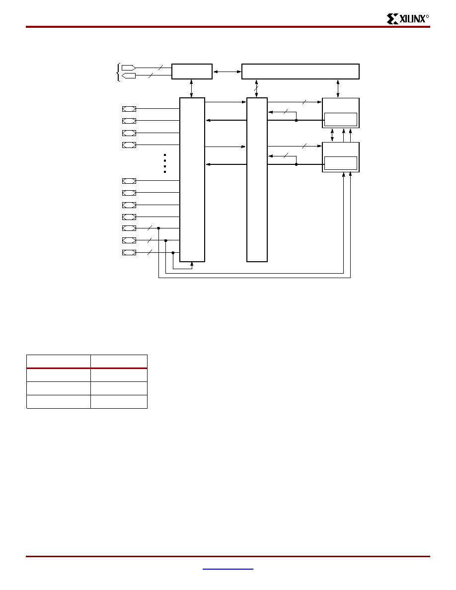
The XC9536XV is a 2.5V CPLD targeted for high-perfor-
mance, low-voltage applications in leading-edge communi-
cations and computing systems. It is comprised of two
54V18 Function Blocks, providing 800 usable gates with
propagation delays of 5 ns. See
Figure 2
for architecture
overview.
Power Estimation
Power dissipation in CPLDs can vary substantially depend-
ing on the system frequency, design application and output
loading. To help reduce power dissipation, each macrocell
in a XC9500XV device may be configured for low-power
mode (from the default high-performance mode). In addi-
tion, unused product-terms and macrocells are automati-
cally deactivated by the software to further conserve power.
For a general estimate of I
CC
, the following equation may be
used:
P
TOTAL
= P
INT
+ P
IO
= I
CCINT
x V
CCINT
+ P
IO
Separating internal and I/O power here is convenient
because XC9500XV CPLDs also separate the correspond-
ing power pins. P
IO
is a strong function of the load capaci-
tance driven, so it is handled by I = CVf. I
CCINT
is another
situation that reflects the actual design considered and the
internal switching speeds. An estimation expression for
I
CCINT
(taken from simulation) is:
I
CCINT
(mA) = MC
HS
(0.122 X PT
HS
+ 0.238) + MC
LP
(0.042 x
PT
LP
+ 0.171) + 0.04(MC
HS
+ MC
LP
) x f
MAX
x MC
TOG
where:
MC
HS
= # macrocells used in high speed mode
MC
LP
= #macrocells used in low power mode
PT
HS
= average p-terms used per high speed macrocell
PT
LP
= average p-terms used over low power macrocell
f
MAX
= max clocking frequency in the device
MC
TOG
= % macrocells toggling on each clock (12% is
frequently a good estimate
This calculation was derived from laboratory measurements
of an XC9500XV part filled with 16-bit counters and allowing
a single output (the LSB) to be enabled. The actual I
CC
value varies with the design application and should be veri-
fied during normal system operation.
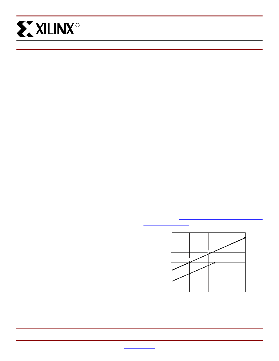
Figure 1
shows the
above estimation in a graphical form. For a more detailed
discussion of power consumption in this device, see Xilinx
application note
XAPP361, "Planning for High Speed
XC9500XV Designs."
0
XC9536XV High-performance
CPLD
DS053 (v2.6) April 15, 2005
0
1
Product Specification
R
Figure 1: Typical I
CC
vs. Frequency for XC9536XV
Clock Frequency (MHz)
Typical I
CC
(mA)
0
100
200
DS053_01_121501
60
20
120 MHz
200 MHz
30
Low
Power
150
50
10
40
50
Hig
h P
erf
orm
anc
e
XC9536XV High-performance CPLD
2
www.xilinx.com
DS053 (v2.6) April 15, 2005
Product Specification
R
Supported I/O Standards
The XC9536XV CPLD features both LVCMOS and LVTTL
I/O implementations. See
Table 1
for I/O standard voltages.
The LVTTL I/O standard is a general purpose EIA/JEDEC
standard for 3.3V applications that use an LVTTL input
buffer and Push-Pull output buffer. The LVCMOS2 standard
is used in 2.5V applications.
XC9500XV CPLDs are also 1.8V I/O compatible. The
X25TO18 setting is provided for generating 1.8V compatible
outputs from a CPLD normally operating in a 2.5V environ-
ment. The default I/O Standard for pads without IOSTAN-
DARD attributes is LVTTL for XC9500XV devices.
Figure 2: XC9536XV Architecture
Function block outputs (indicated by the bold line) drive the I/O Blocks directly.
In-System Programming Controller
JTAG
Controller
I/O
Blocks
Function
Block 1
Macrocells
1 to 18
Macrocells
1 to 18
JTAG Port
3
54
I/O/GTS
I/O/GSR
I/O/GCK
I/O
I/O
I/O
I/O
2
1
I/O
I/O
I/O
I/O
3
DS053_02_041200
1
Function
Block 2
54
18
18
Fast CONNECT II Switch Matrix
Table 1: IOSTANDARD Options
IOSTANDARD
V
CCIO
LVTTL
3.3V
LVCMOS2
2.5V
X25TO18
1.8V
XC9536XV High-performance CPLD
DS053 (v2.6) April 15, 2005
www.xilinx.com
3
Product Specification
R
Absolute Maximum Ratings
Recommended Operation Conditions
Quality and Reliability Characteristics
Symbol
Description
Value
Units
V
CC
Supply voltage relative to GND
≠0.5 to 2.7
V
V
CCIO
Supply voltage for output drivers
≠0.5 to 3.6
V
V
IN
Input voltage relative to GND
(1)
≠0.5 to 3.6
V
V
TS
Voltage applied to 3-state output
(1)
≠0.5 to 3.6
V
T
STG
Storage temperature (ambient)
≠65 to +150
o
C
T
J
Junction temperature
+150
o
C
Notes:
1.
Maximum DC undershoot below GND must be limited to either 0.5V or 10 mA, whichever is easier to achieve. During transitions, the
device pins may undershoot to ≠2.0V or overshoot to +3.6V, provided this over- or undershoot lasts less than 10 ns and with the
forcing current being limited to 200 mA.
2.
Stresses beyond those listed under Absolute Maximum Ratings may cause permanent damage to the device. These are stress
ratings only, and functional operation of the device at these or any other conditions beyond those listed under Operating Conditions
is not implied. Exposure to Absolute Maximum Ratings conditions for extended periods of time may affect device reliability.
3.
For solder specifications, see
Xilinx Packaging
.
Symbol
Parameter
Min
Max
Units
V
CCINT
Supply voltage for internal logic
and input buffers
Commercial T
A
= 0
o
C to +70
o
C
2.37
2.62
V
Industrial T
A
= ≠40
o
C to +85
o
C
2.37
2.62
V
CCIO
Supply voltage for output drivers for 3.3V operation
3.0
3.6
V
Supply voltage for output drivers for 2.5V operation
2.37
2.62
V
Supply voltage for output drivers for 1.8V operation
1.71
1.89
V
V
IL
Low-level input voltage
0
0.8
V
V
IH
High-level input voltage
1.7
3.6
V
V
O
Output voltage
0
V
CCIO
V
Symbol
Parameter
Min
Max
Units
T
DR
Data Retention
20
-
Years
N
PE
Program/Erase Cycles (Endurance)
1,000
-
Cycles
V
ESD
Electrostatic Discharge (ESD)
2,000
-
Volts

XC9536XV High-performance CPLD
4
www.xilinx.com
DS053 (v2.6) April 15, 2005
Product Specification
R
DC Characteristics
(Over Recommended Operating Conditions)
AC Characteristics
Symbol
Parameter
Test Conditions
Min
Max
Units
V
OH
Output high voltage for 3.3V outputs
I
OH
= ≠4.0 mA
2.4
-
V
Output high voltage for 2.5V outputs
I
OH
= ≠1.0 mA
2.0
-
V
Output high voltage for 1.8V outputs
I
OH
= ≠100
µ
A
90% V
CCIO
-
V
V
OL
Output low voltage for 3.3V outputs
I
OL
= 8.0 mA
-
0.4
V
Output low voltage for 2.5V outputs
I
OL
= 1.0 mA
-
0.4
V
Output low voltage for 1.8V outputs
I
OL
= 100
µ
A
-
0.4
V
I
IL
Input leakage current
V
CC
= 2.62V
V
CCIO
= 3.6V
V
IN
= GND or 3.6V
-
±10
µ
A
I
IH
Input high-Z leakage current
V
CC
= 2.62V
V
CCIO
= 3.6V
V
IN
= GND or 3.6V
-
±10
µ
A
V
CC
min < V
IN
< 3.6V
-
±150
µ
A
C
IN
I/O capacitance
V
IN
= GND
f = 1.0 MHz
-
10
pF
I
CC
Operating Supply Current
(low power mode, active)
V
I
= GND, No load
f = 1.0 MHz
7
mA
Symbol
Parameter
XC9536XV-5
XC9536XV-7
Units
Min
Max
Min
Max
T
PD
I/O to output valid
-
5.0
-
7.5
ns
T
SU
I/O setup time before GCK
3.5
-
4.8
-
ns
T
H
I/O hold time after GCK
0
-
0
-
ns
T
CO
GCK to output valid
-
3.5
-
4.5
ns
f
SYSTEM
Multiple FB internal operating frequency
-
222.2
-
125.0
MHz
T
PSU
I/O setup time before p-term clock input
1.0
-
1.6
-
ns
T
PH
I/O hold time after p-term clock input
2.5
-
3.2
-
ns
T
PCO
P-term clock output valid
-
6.0
-
7.7
ns
T
OE
GTS to output valid
-
4.0
-
5.0
ns
T
OD
GTS to output disable
-
4.0
-
5.0
ns
T
POE
Product term OE to output enabled
-
7.0
-
9.5
ns
T
POD
Product term OE to output disabled
-
7.0
-
9.5
ns
T
AO
GSR to output valid
-
10.0
-
12.0
ns
T
PAO
P-term S/R to output valid
-
10.7
-
12.6
ns
T
WLH
GCK pulse width (High or Low)
2.2
-
4.0
-
ns
T
PLH
P-term clock pulse width (High or Low)
5.0
-
6.5
-
ns
T
APRPW
Asynchronous preset/reset pulse width (High or Low)
5.0
-
6.5
-
ns
XC9536XV High-performance CPLD
DS053 (v2.6) April 15, 2005
www.xilinx.com
5
Product Specification
R
Internal Timing Parameters
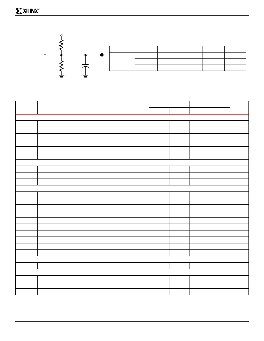
Figure 3: AC Load Circuit
Symbol
Parameter
XC9536XV-5
XC9536XV-7
Units
Min
Max
Min
Max
Buffer Delays
T
IN
Input buffer delay
-
2.0
-
2.3
ns
T
GCK
GCK buffer delay
-
1.2
-
1.5
ns
T
GSR
GSR buffer delay
-
2.0
-
3.1
ns
T
GTS
GTS buffer delay
-
4.0
-
5.0
ns
T
OUT
Output buffer delay
-
2.1
-
2.5
ns
T
EN
Output buffer enable/disable delay
-
0
-
0
ns
Product Term Control Delays
T
PTCK
Product term clock delay
-
1.7
-
2.4
ns
T
PTSR
Product term set/reset delay
-
0.7
-
1.4
ns
T
PTTS
Product term 3-state delay
-
5.0
-
7.2
ns
Internal Register and Combinatorial Delays
T
PDI
Combinatorial logic propagation delay
-
0.2
-
1.3
ns
T
SUI
Register setup time
2.0
-
2.6
-
ns
T
HI
Register hold time
1.5
-
2.2
-
ns
T
ECSU
Register clock enable setup time
2.0
-
2.6
-
ns
T
ECHO
Register clock enable hold time
1.5
-
2.2
-
ns
T
COI
Register clock to output valid time
-
0.2
-
0.5
ns
T
AOI
Register async. S/R to output delay
-
5.9
-
6.4
ns
T
RAI
Register async. S/R recover before clock
5.0
7.5
ns
T
LOGI
Internal logic delay
-
0.7
-
1.4
ns
T
LOGILP
Internal low power logic delay
-
5.7
-
6.4
ns
Feedback Delays
T
F
Fast CONNECT II feedback delay
-
1.6
-
3.5
ns
Time Adders
T
PTA
Incremental product term allocator delay
-
0.7
-
0.8
ns
T
PTA2
Adjacent macrocell p-term allocator delay
-
0.3
-
0.3
ns
T
SLEW
Slew-rate limited delay
-
3.0
-
4.0
ns
R
1
V
TEST
C
L
R
2
Device Output
Output Type
V
TEST
3.3V
2.5V
1.8V
R
1
320
250
10K
R
2
360
660
14K
C
L
35 pF
35 pF
35 pF
DS051_03_0601000
V
CCIO
3.3V
2.5V
1.8V