DS123 (v2.6) March 14, 2005
www.xilinx.com
1
Preliminary Product Specification
� 2005 Xilinx, Inc. All rights reserved. All Xilinx trademarks, registered trademarks, patents, and disclaimers are as listed at
http://www.xilinx.com/legal.htm
.
All other trademarks and registered trademarks are the property of their respective owners. All specifications are subject to change without notice.
Features
�
In-System Programmable PROMs for Configuration of
Xilinx FPGAs
�
Low-Power Advanced CMOS NOR FLASH Process
�
Endurance of 20,000 Program/Erase Cycles
�
Operation over Full Industrial Temperature Range
(�40�C to +85�C)
�
IEEE Standard 1149.1/1532 Boundary-Scan (JTAG)
Support for Programming, Prototyping, and Testing
�
JTAG Command Initiation of Standard FPGA
Configuration
�
Cascadable for Storing Longer or Multiple Bitstreams
�
Dedicated Boundary-Scan (JTAG) I/O Power Supply
(V
CCJ
)
�
I/O Pins Compatible with Voltage Levels Ranging From
1.5V to 3.3V
�
Design Support Using the Xilinx Alliance ISE and
Foundation ISE Series Software Packages
�
XCF01S/XCF02S/XCF04S
-
3.3V supply voltage
-
Serial FPGA configuration interface (up to 33 MHz)
-
Available in small-footprint VO20 and VOG20
packages.
�
XCF08P/XCF16P/XCF32P
-
1.8V supply voltage
-
Serial or parallel FPGA configuration interface
(up to 33 MHz)
-
Available in small-footprint VO48, VOG48, FS48,
and FSG48 packages
-
Design revision technology enables storing and
accessing multiple design revisions for
configuration
-
Built-in data decompressor compatible with Xilinx
advanced compression technology
Description
Xilinx introduces the Platform Flash series of in-system pro-
grammable configuration PROMs. Available in 1 to 32
Megabit (Mbit) densities, these PROMs provide an
easy-to-use, cost-effective, and reprogrammable method
for storing large Xilinx FPGA configuration bitstreams. The
Platform Flash PROM series includes both the 3.3V
XCFxxS PROM and the 1.8V XCFxxP PROM. The XCFxxS
version includes 4-Mbit, 2-Mbit, and 1-Mbit PROMs that
support Master Serial and Slave Serial FPGA configuration
modes (
Figure 1
). The XCFxxP version includes 32-Mbit,
16-Mbit, and 8-Mbit PROMs that support Master Serial,
Slave Serial, Master SelectMAP, and Slave SelectMAP
FPGA configuration modes (
Figure 2
). A summary of the
Platform Flash PROM family members and supported fea-
tures is shown in
Table 1
.
4
2
Platform Flash In-System Programmable
Configuration PROMS
DS123 (v2.6) March 14, 2005
0
Preliminary Product Specification
R
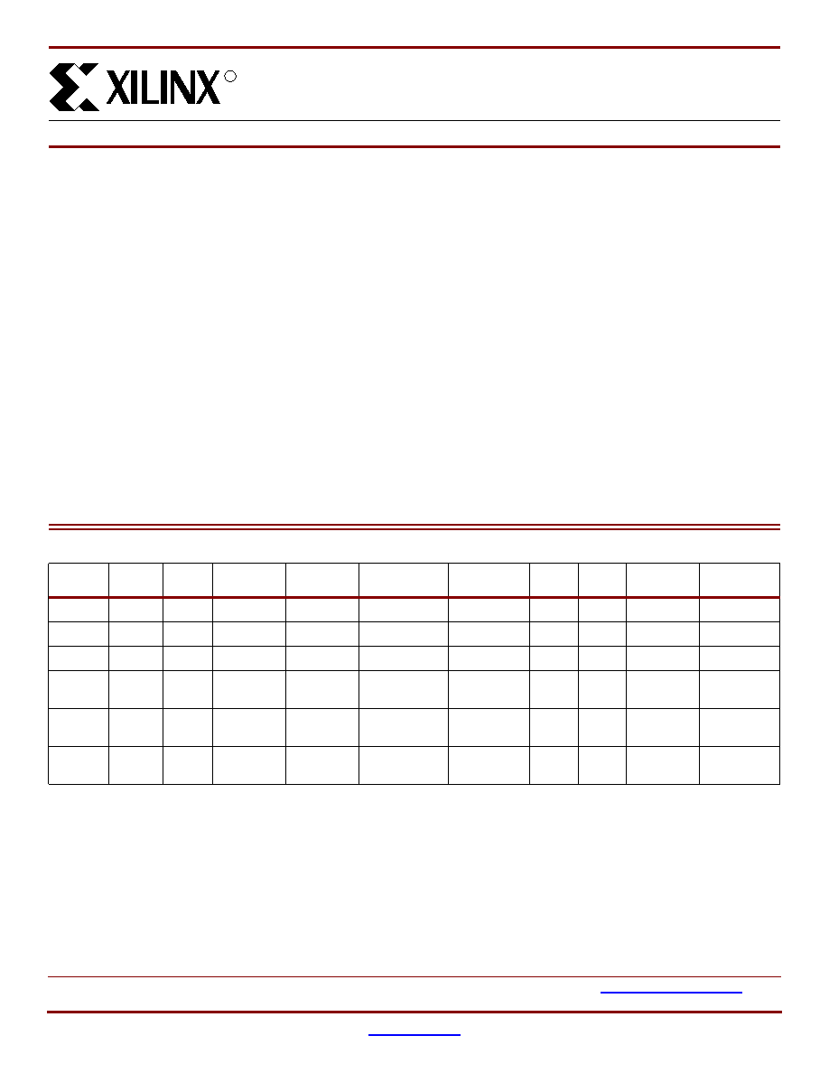
Table 1: Platform Flash PROM Features
Density
V
CCINT
V
CCO
Range V
CCJ
Range
Packages
JTAG ISP
Programming
Serial
Config.
Parallel
Config.
Design
Revisioning
Compression
XCF01S
1 Mbit
3.3V
1.8V - 3.3V
2.5V - 3.3V
VO20/VOG20
XCF02S
2 Mbit
3.3V
1.8V
- 3.3V
2.5V - 3.3V
VO20/VOG20
XCF04S
4 Mbit
3.3V
1.8V
- 3.3V
2.5V - 3.3V
VO20/VOG20
XCF08P
8 Mbit
1.8V
1.5V
- 3.3V
2.5V - 3.3V
VO48/VOG48
FS48/FSG48
XCF16P
16 Mbit
1.8V
1.5V - 3.3V
2.5V - 3.3V
VO48/VOG48
FS48/FSG48
XCF32P
32 Mbit
1.8V
1.5V - 3.3V
2.5V - 3.3V
VO48/VOG48
FS48/FSG48

Platform Flash In-System Programmable Configuration PROMS
DS123 (v2.6) March 14, 2005
www.xilinx.com
2
Preliminary Product Specification
R
When the FPGA is in Master Serial mode, it generates a
configuration clock that drives the PROM. With CF High, a
short access time after CE and OE are enabled, data is
available on the PROM DATA (D0) pin that is connected to
the FPGA DIN pin. New data is available a short access
time after each rising clock edge. The FPGA generates the
appropriate number of clock pulses to complete the config-
uration.
When the FPGA is in Slave Serial mode, the PROM and the
FPGA are both clocked by an external clock source, or
optionally, for the XCFxxP PROM only, the PROM can be
used to drive the FPGA's configuration clock.
The XCFxxP version of the Platform Flash PROM also sup-
ports Master SelectMAP and Slave SelectMAP (or Slave
Parallel) FPGA configuration modes. When the FPGA is in
Master SelectMAP mode, the FPGA generates a configura-
tion clock that drives the PROM. When the FPGA is in Slave
SelectMAP Mode, either an external oscillator generates
the configuration clock that drives the PROM and the
FPGA, or optionally, the XCFxxP PROM can be used to
drive the FPGA's configuration clock. With BUSY Low and
CF High, after CE and OE are enabled, data is available on
the PROMs DATA (D0-D7) pins. New data is available a
short access time after each rising clock edge. The data is
clocked into the FPGA on the following rising edge of the
CCLK. A free-running oscillator can be used in the Slave
Parallel /Slave SelecMAP mode.
The XCFxxP version of the Platform Flash PROM provides
additional advanced features. A built-in data decompressor
supports utilizing compressed PROM files, and design revi-
sioning allows multiple design revisions to be stored on a
single PROM or stored across several PROMs. For design
revisioning, external pins or internal control bits are used to
select the active design revision.
Multiple Platform Flash PROM devices can be cascaded to
support the larger configuration files required when target-
ing larger FPGA devices or targeting multiple FPGAs daisy
chained together. When utilizing the advanced features for
the XCFxxP Platform Flash PROM, such as design revi-
sioning, programming files which span cascaded PROM
devices can only be created for cascaded chains containing
only XCFxxP PROMs. If the advanced XCFxxP features are
Figure 1: XCFxxS Platform Flash PROM Block Diagram
Control
and
JTAG
Interface
Memory
Serial
Interface
DATA (D0)
Serial Mode
Data
Address
CLK
CE
TCK
TMS
TDI
TDO
OE/RESET
CEO
Data
ds123_01_30603
CF
FI
Figure 2: XCFxxP Platform Flash PROM Block Diagram
CLKOUT
CEO
DATA (D0)
(Serial/Parallel Mode)
D[1:7]
(Parallel Mode)
TCK
TMS
TDI
TDO
CLK
CE
EN_EXT_SEL
OE/RESET
BUSY
Data
Data
Address
REV_SEL [1:0]
CF
Control
and
JTAG
Interface
Memory
OSC
Serial
or
Parallel
Interface
Decompressor
ds123_19_050604

Platform Flash In-System Programmable Configuration PROMS
DS123 (v2.6) March 14, 2005
www.xilinx.com
3
Preliminary Product Specification
R
not enabled, then the cascaded chain can include both
XCFxxP and XCFxxS PROMs.
The Platform Flash PROMs are compatible with all of the
existing FPGA device families. A reference list of Xilinx
FPGAs and the respective compatible Platform Flash
PROMs is given in
Table 2
. A list of Platform Flash PROMs
and their capacities is given in
Table 3
.
Table 2: Xilinx FPGAs and Compatible Platform Flash
PROMs
FPGA
Configuration
Bitstream
Platform Flash
PROM
(1)
Virtex-4 LX
XC4VLX15
4,765,185
XCF08P
XC4VLX25
7,819,520
XCF08P
XC4VLX40
12,259,328
XCF16P
XC4VLX60
17,717,248
XCF32P
XC4VLX80
23,290,624
XCF32P
XC4VLX100
30,711,296
XCF32P
XC4VLX160
40,346,624
XCF32P+XCF08P
XC4VLX200
48,722,432
XCF32P+XCF16P
Virtex-4 FX
XC4VFX12
4,765,184
XCF08P
XC4VFX20
7,242,240
XCF08P
XC4VFX40
13,550,336
XCF16P
XC4VFX60
21,002,496
XCF32P
XC4VFX100
33,065,024
XCF32P
XC4VFX140
47,856,512
XCF32P+XCF16P
Virtex-4 SX
XC4VSX25
9,147,264
XCF16P
XC4VSX35
13,669,904
XCF16P
XC4VSX55
22,744,832
XCF32P
Virtex-II Pro X
XC2VPX20
8,214,560
XCF08P
XC2VPX70
26,098,976
XCF32P
Virtex-II Pro
XC2VP2
1,305,376
XCF02S
XC2VP4
3,006,496
XCF04S
XC2VP7
4,485,408
XCF08P
XC2VP20
8,214,560
XCF08P
XC2VP30
11,589,920
XCF16P
XC2VP40
15,868,192
XCF16P
XC2VP50
19,021,344
XCF32P
XC2VP70
26,098,976
XCF32P
XC2VP100
34,292,768
XCF32P
(2)
Virtex-II
(3)
XC2V40
360,096
XCF01S
XC2V80
635,296
XCF01S
XC2V250
1,697,184
XCF02S
XC2V500
2,761,888
XCF04S
XC2V1000
4,082,592
XCF04S
XC2V1500
5,659,296
XCF08P
XC2V2000
7,492,000
XCF08P
XC2V3000
10,494,368
XCF16P
XC2V4000
15,659,936
XCF16P
XC2V6000
21,849,504
XCF32P
XC2V8000
29,063,072
XCF32P
Virtex-E
XCV50E
630,048
XCF01S
XCV100E
863,840
XCF01S
XCV200E
1,442,016
XCF02S
XCV300E
1,875,648
XCF02S
XCV400E
2,693,440
XCF04S
XCV405E
3,430,400
XCF04S
XCV600E
3,961,632
XCF04S
XCV812E
6,519,648
XCF08P
XCV1000E
6,587,520
XCF08P
XCV1600E
8,308,992
XCF08P
XCV2000E
10,159,648
XCF16P
XCV2600E
12,922,336
XCF16P
XCV3200E
16,283,712
XCF16P
Virtex
XCV50
559,200
XCF01S
XCV100
781,216
XCF01S
XCV150
1,040,096
XCF01S
XCV200
1,335,840
XCF02S
XCV300
1,751,808
XCF02S
XCV400
2,546,048
XCF04S
XCV600
3,607,968
XCF04S
XCV800
4,715,616
XCF08P
XCV1000
6,127,744
XCF08P
Spartan-3E
XC3S100E
581,344
XCF01S
XC3S250E
1,352,192
XCF02S
XC3S500E
2,267,136
XCF04S
XC3S1200E
3,832,320
XCF04S
XC3S1600E
5,957,760
XCF08P
Spartan-3L
XC3S1000L
3,223,488
XCF04S
XC3S1500L
5,214,784
XCF08P
XC3S5000L
13,271,936
XCF16P
Table 2: Xilinx FPGAs and Compatible Platform Flash
PROMs (Continued)
FPGA
Configuration
Bitstream
Platform Flash
PROM
(1)

Platform Flash In-System Programmable Configuration PROMS
DS123 (v2.6) March 14, 2005
www.xilinx.com
4
Preliminary Product Specification
R
Programming
In-System Programming
In-System Programmable PROMs can be programmed
individually, or two or more can be daisy-chained together
and programmed in-system via the standard 4-pin JTAG
protocol as shown in
Figure 3
. In-system programming
offers quick and efficient design iterations and eliminates
unnecessary package handling or socketing of devices. The
programming data sequence is delivered to the device
using either Xilinx iMPACT software and a Xilinx download
cable, a third-party JTAG development system, a
JTAG-compatible board tester, or a simple microprocessor
interface that emulates the JTAG instruction sequence. The
iMPACT software also outputs serial vector format (SVF)
files for use with any tools that accept SVF format, including
automatic test equipment. During in-system programming,
the CEO output is driven High. All other outputs are held in
a high-impedance state or held at clamp levels during
in-system programming. In-system programming is fully
supported across the recommended operating voltage and
temperature ranges.
OE/RESET
The 1/2/4 Mbit XCFxxS Platform Flash PROMs in-system
programming algorithm results in issuance of an internal
device reset that causes OE/RESET to pulse Low.
External Programming
Xilinx reprogrammable PROMs can also be programmed by
the Xilinx MultiPRO Desktop Tool or a third-party device
programmer. This provides the added flexibility of using
pre-programmed devices with an in-system programmable
option for future enhancements and design changes.
Reliability and Endurance
Xilinx in-system programmable products provide a guaran-
teed endurance level of 20,000 in-system program/erase
cycles and a minimum data retention of 20 years. Each
device meets all functional, performance, and data retention
specifications within this endurance limit.
Design Security
The Xilinx in-system programmable Platform Flash PROM
devices incorporate advanced data security features to fully
protect the FPGA programming data against unauthorized
reading via JTAG. The XCFxxP PROMs can also be pro-
Spartan-3
XC3S50
439,264
XCF01S
XC3S200
1,047,616
XCF01S
XC3S400
1,699,136
XCF02S
XC3S1000
3,223,488
XCF04S
XC3S1500
5,214,784
XCF08P
XC3S2000
7,673,024
XCF08P
XC3S4000
11,316,864
XCF16P
XC3S5000
13,271,936
XCF16P
Spartan-IIE
XC2S50E
630,048
XCF01S
XC2S100E
863,840
XCF01S
XC2S150E
1,134,496
XCF02S
XC2S200E
1,442,016
XCF02S
XC2S300E
1,875,648
XCF02S
XC2S400E
2,693,440
XCF04S
XC2S600E
3,961,632
XCF04S
Spartan-II
XC2S15
197,696
XCF01S
XC2S30
336,768
XCF01S
XC2S50
559,200
XCF01S
XC2S100
781,216
XCF01S
XC2S150
1,040,096
XCF01S
XC2S200
1,335,840
XCF02S
Notes:
1.
If design revisioning or other advanced feature support is required,
the XCFxxP can be used as an alternative to the XCF01S, XCF02S,
or XCF04S.
2.
Assumes compression used.
3.
The largest possible Virtex-II bitstream sizes are specified. Refer to
the Virtex-II User Guide for information on bitgen options which
affect bitstream size.
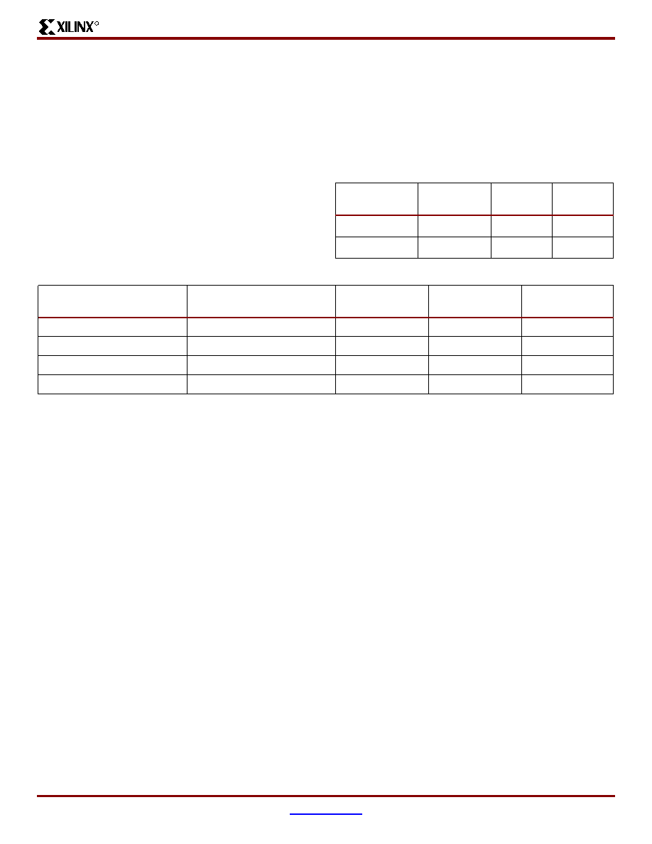
Table 3: Platform Flash PROM Capacity
Platform
Flash PROM
Configuration
Bits
Platform Flash
PROM
Configuration
Bits
XCF01S
1,048,576 XCF08P
8,388,608
XCF02S
2,097,152 XCF16P
16,777,216
XCF04S
4,194,304 XCF32P
33,554,432
Table 2: Xilinx FPGAs and Compatible Platform Flash
PROMs (Continued)
FPGA
Configuration
Bitstream
Platform Flash
PROM
(1)
Figure 3: JTAG In-System Programming Operation
(a) Solder Device to PCB
(b) Program Using Download Cable
DS026_02_082703
GND
V
CC
(a)
(b)
Platform Flash In-System Programmable Configuration PROMS
DS123 (v2.6) March 14, 2005
www.xilinx.com
5
Preliminary Product Specification
R
grammed to prevent inadvertent writing via JTAG.
Table 4
and
Table 5
show the security settings available for the
XCFxxS PROM and XCFxxP PROM, respectively.
Read Protection
The read protect security bit can be set by the user to pre-
vent the internal programming pattern from being read or
copied via JTAG. Read protection does not prevent write
operations. For the XCFxxS PROM, the read protect secu-
rity bit is set for the entire device, and resetting the read pro-
tect security bit requires erasing the entire device. For the
XCFxxP PROM the read protect security bit can be set for
individual design revisions, and resetting the read protect
bit requires erasing the particular design revision.
Write Protection
The XCFxxP PROM device also allows the user to write
protect (or lock) a particular design revision to prevent inad-
vertent erase or program operations. Once set, the write
protect security bit for an individual design revision must be
reset (using the UNLOCK command followed by
ISC_ERASE command) before an erase or program opera-
tion can be performed.
IEEE 1149.1 Boundary-Scan (JTAG)
The Platform Flash PROM family is IEEE Standard 1532
in-system programming compatible, and is fully compliant
with the IEEE Std. 1149.1 Boundary-Scan, also known as
JTAG, which is a subset of IEEE Std. 1532 Boundary-Scan.
A Test Access Port (TAP) and registers are provided to sup-
port all required boundary scan instructions, as well as
many of the optional instructions specified by IEEE Std.
1149.1. In addition, the JTAG interface is used to implement
in-system programming (ISP) to facilitate configuration, era-
sure, and verification operations on the Platform Flash
PROM device.
Table 6
lists the required and optional
boundary-scan instructions supported in the Platform Flash
PROMs. Refer to the IEEE Std. 1149.1 specification for a
complete description of boundary-scan architecture and the
required and optional instructions.
Instruction Register
The Instruction Register (IR) for the Platform Flash PROM
is connected between TDI and TDO during an instruction
scan sequence. In preparation for an instruction scan
sequence, the instruction register is parallel loaded with a
fixed instruction capture pattern. This pattern is shifted out
onto TDO (LSB first), while an instruction is shifted into the
instruction register from TDI.
XCFxxS Instruction Register (8 bits wide)
The Instruction Register (IR) for the XCFxxS PROM is eight
bits wide and is connected between TDI and TDO during an
instruction scan sequence. The detailed composition of the
instruction capture pattern is illustrated in
Figure 4
. The
instruction capture pattern shifted out of the XCFxxS device
includes IR[7:0]. IR[7:5] are reserved bits and are set to a
logic "0". The ISC Status field, IR[4], contains logic "1" if the
device is currently in In-System Configuration (ISC) mode;
otherwise, it contains logic "0". The Security field, IR[3],
contains logic "1" if the device has been programmed with
the security option turned on; otherwise, it contains logic
"0". IR[2] is unused, and is set to '0'. The remaining bits
IR[1:0] are set to '01' as defined by IEEE Std. 1149.1.
XCFxxP Instruction Register (16 bits wide)
The Instruction Register (IR) for the XCFxxP PROM is six-
teen bits wide and is connected between TDI and TDO dur-
ing an instruction scan sequence. The detailed composition
of the instruction capture pattern is illustrated in
Figure 5
.
The instruction capture pattern shifted out of the XCFxxP
device includes IR[15:0]. IR[15:9] are reserved bits and are
set to a logic "0". The ISC Error field, IR[8:7], contains a "10"
when an ISC operation is a success; otherwise a "01" when
an In-System Configuration (ISC) operation fails. The
Erase/Program (ER/PROG) Error field, IR[6:5], contains a
"10" when an erase or program operation is a success; oth-
Table 4: XCFxxS Device Data Security Options
Read Protect
Read/Verify
Inhibited
Program
Inhibited
Erase
Inhibited
Reset (default)
Set
Table 5: XCFxxP Design Revision Data Security Options
Read Protect
Write Protect
Read/Verify
Inhibited
Program
Inhibited
Erase Inhibited
Reset (default)
Reset (default)
Reset (default)
Set
Set
Reset (default)
Set
Set