Äîêóìåíòàöèÿ è îïèñàíèÿ www.docs.chipfind.ru

DS047 (v1.1) February 10, 2000
www.xilinx.com
1
1-800-255-7778
Features
·
Industry's first TotalCMOSTM SPLD - both CMOS
design and process technologies
·
Fast Zero Power (FZPTM) design technique provides
ultra-low power and high speed
-
Static current of less than 45
µ
A
-
Dynamic current substantially below that of
competing devices
-
Pin-to-pin delay of only 10 ns
·
True Zero Power device with no turbo bits or power
down schemes
·
Function/JEDEC map compatible with Bipolar,
UVCMOS, EECMOS 22V10s
·
Multiple packaging options featuring PCB-friendly
flow-through pinouts (SOL and TSSOP)
-
24-pin TSOICuses 93% less in-system space than
a 28-pin PLCC
-
24-pin SOIC
-
28-pin PLCC with standard JEDEC pinout
·
Available in commercial and industrial operating ranges
·
Supports mixed voltage systems--5V tolerant I/Os
·
Advanced 0.5
µ
E
2
CMOS process
·
1000 erase/program cycles guaranteed
·
20 years data retention guaranteed
·
Varied product term distribution with up to 16 product
terms per output for complex functions
·
Programmable output polarity
·
Synchronous preset/asynchronous reset capability
·
Security bit prevents unauthorized access
·
Electronic signature for identification
·
Design entry and verification using industry standard
CAE tools
·
Reprogrammable using industry standard device
programmers
Description
The XCR22LV10 is the first SPLD to combine high perfor-
mance with low power, without the need for "turbo bits" or
other power down schemes. To achieve this, Xilinx has
used their FZP design technique, which replaces conven-
tional sense amplifier methods for implementing product
terms (a technique that has been used in PLDs since the
bipolar era) with a cascaded chain of pure CMOS gates.
This results in the combination of low power and high
speed that has previously been unattainable in the PLD
arena. For 5V operation, Xilinx offers the XCR22V10 that
offers high speed and low power in a 5V implementation.
The XCR22LV10 uses the familiar AND/OR logic array
structure, which allows direct implementation of
sum-of-products equations. This device has a programma-
ble AND array which drives a fixed OR array. The OR sum
of products feeds an "Output Macro Cell" (OMC), which can
be individually configured as a dedicated input, a combina-
torial output, or a registered output with internal feedback.
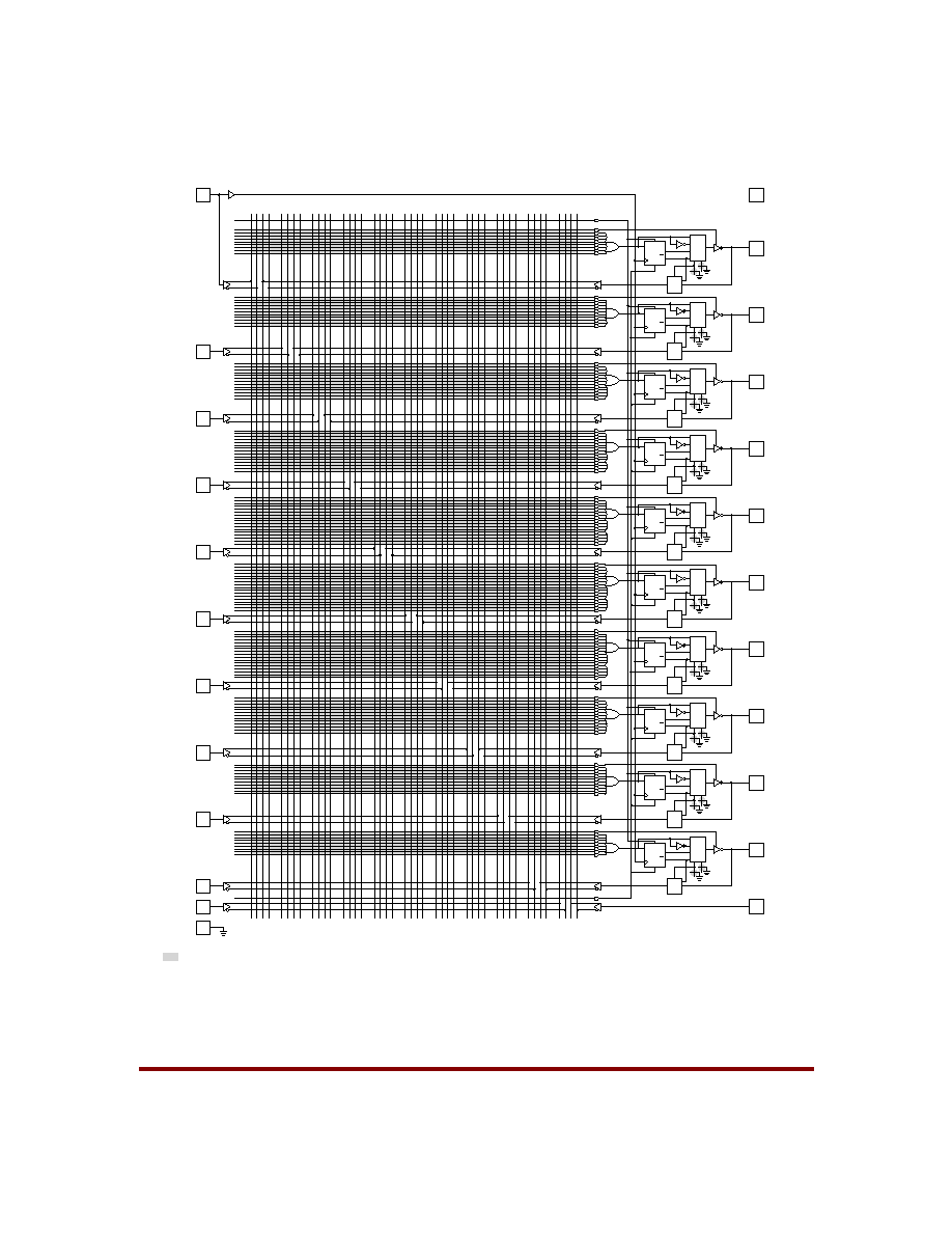
Functional Description
The XCR22LV10 implements logic functions as
sum-of-products expressions in a programmable-
AND/fixed-OR logic array. User-defined functions are cre-
ated by programming the connections of input signals into
the array. User-configurable output structures in the form of
I/O macrocells further increase logic flexibility (
Figure 1
).
0
XCR22LV10: 3V Zero Power,
TotalCMOS, Universal PLD Device
DS047 (v1.1) February 10, 2000
0
0*
Product Specification
R
DS047 (v1.1) February 10, 2000
www.xilinx.com
2
1-800-255-7778
.
Figure 1: XCR22LV10 Logic Diagram
NOTE:
Programmable connection.
1
1
0
0
0
1
0
1
DAR
Q
Q
SP
0
1
Q
1
1
0
0
0
1
0
1
DAR
Q
SP
0
1
Q
1
1
0
0
0
1
0
1
DAR
Q
SP
0
1
Q
1
1
0
0
0
1
0
1
DAR
Q
SP
0
1
Q
1
1
0
0
0
1
0
1
DAR
Q
SP
0
1
Q
1
1
0
0
0
1
0
1
DAR
Q
SP
0
1
Q
1
1
0
0
0
1
0
1
DAR
Q
SP
0
1
Q
1
1
0
0
0
1
0
1
DAR
Q
SP
0
1
Q
1
1
0
0
0
1
0
1
DAR
Q
SP
0
1
Q
1
1
0
0
0
1
0
1
DAR
Q
SP
0
1
AR
SP
0
3
4
7
8
11 12
15 16
19 20
23 24
27 28
31 32
35 36
39 40
43
0
3
4
7
8
11 12
15 16
19 20
23 24
27 28
31 32
35 36
39 40
43
1
2
3
4
5
6
7
8
9
10
11
12
24
23
22
21
20
19
18
17
16
15
14
13
CLK/I0
I1
I2
I3
I4
I5
I6
I7
I10
I8
I9
GND
I11
F0
F1
F2
F3
F4
F5
F6
F7
F8
F9
VCC
0
1
9
10
20
21
33
34
48
49
65
66
82
83
97
98
110
111
121
122
130
131
SP00059
R
XCR22LV10: 3V Zero Power, TotalCMOS, Universal PLD
3
www.xilinx.com
DS047 (v1.1) February 10, 2000
1-800-255-7778
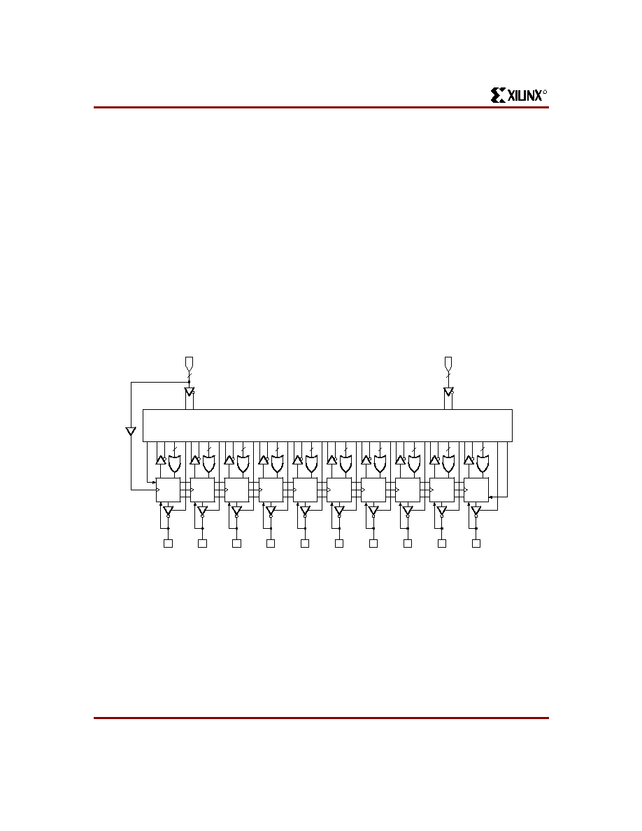
Architecture Overview
The XCR22LV10 architecture is illustrated in Figure. Twelve
dedicated inputs and ten I/Os provide up to 22 inputs and
ten outputs for creation of logic functions. At the core of the
device is a programmable electrically-erasable AND array
which drives a fixed-OR array. With this structure, the
XCR22LV10 can implement up to ten sum-of-products logic
expressions.
Associated with each of the ten OR functions is an I/O mac-
rocell which can be independently programmed to one of
four different configurations. The programmable macrocells
allow each I/O to create sequential or combinatorial logic
functions with either active High or active Low polarity.
AND/OR Logic Array
The programmable AND array of the XCR22LV10 (shown
in the Logic Diagram,
Figure 1
) is formed by input lines
intersecting product terms. The input lines and product
terms are used as follows:
44 input lines:
·
24 input lines carry the True and Complement of the
signals applied to the 12 input pins
·
20 additional lines carry the True and Complement
values of feedback or input signals from the ten I/Os
·
132 product terms:
·
120 product terms (arranged in two groups of 8, 10, 12,
14, and 16) used to form logical sums
·
Ten output enable terms (one for each I/O)
·
One global synchronous preset product term
·
One global asynchronous clear product term
At each input-line/product-term intersection there is an
EEPROM memory cell which determines whether or not
there is a logical connection at that intersection. Each prod-
uct term is essentially a 44-input AND gate. A product term
which is connected to both the True and Complement of an
input signal will always be FALSE, and thus will not affect
the OR function that it drives. When all the connections on
a product term are opened, a Don't Care state exists and
that term will always be TRUE.
Variable Product Term Distribution
The XCR22LV10 provides 120 product terms to drive the
ten OR functions. These product terms are distributed
among the outputs in groups of 8, 10, 12, 14, and 16 to
form logical sums (see Logic Diagram). This distribution
allows optimum use of device resources.
Programmable I/O Macrocell
The output macrocell provides complete control over the
architecture of each output. the ability to configure each
output independently permits users to tailor the configura-
tion of the XCR22LV10 to the precise requirements of their
designs.
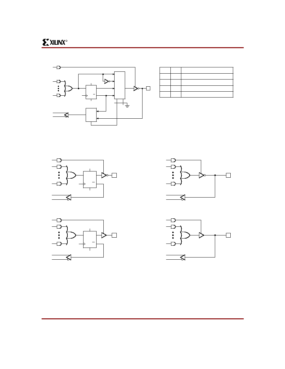
Macrocell Architecture
Each I/O macrocell, as shown in
Figure 3
consists of a
D-type flip-flop and two signal-select multiplexers. The con-
figuration of each macrocell of the XCR22LV10 is deter-
mined by the two EEPROM bits controlling these
multiplexers. These bits determine output polarity, and out-
put type (registered or non-registered). Equivalent circuits
for the macrocell configurations are illustrated in
Figure 4
.
Figure 2: Functional Diagram
OUTPUT
MACRO
CELL
CLK/I0
I1 I11
F0
F1
F2
F3
F4
F5
F6
F7
F8
F9
PROGRAMMABLE AND ARRAY
(44
×
132)
1
11
8
10
12
14
16
16
14
12
10
8
SP00060A
OUTPUT
MACRO
CELL
OUTPUT
MACRO
CELL
OUTPUT
MACRO
CELL
OUTPUT
MACRO
CELL
OUTPUT
MACRO
CELL
OUTPUT
MACRO
CELL
OUTPUT
MACRO
CELL
OUTPUT
MACRO
CELL
OUTPUT
MACRO
CELL
RESET
PRESET
R
XCR22LV10: 3V Zero Power, TotalCMOS, Universal PLD
DS047 (v1.1) February 10, 2000
www.xilinx.com
4
1-800-255-7778
.
Figure 3: Output Macrocell Logic Diagram
F
0
1
1
0
0
1
0
0
1
CLK
1
AR
SP
S1
S0
S
1
S
0
OUTPUT CONFIGURATION
0 = Unprogrammed fuse
1 = Programmed fuse
D
Q
Q
0
0
1
1
0
1
0
1
Registered/Active-LOW/Macrocell feedback
Registered/Active-HIGH/Macrocell feedback
Combinatorial/Active-LOW/Pin feedback
Combinatorial/Active-HIGH/Pin feedback
SP00484
Figure 4: Output Macrocell Configurations
F
CLK
AR
SP
S0 = 0
S1 = 0
D
Q
Q
a. Registered/Active-LOW
F
CLK
AR
SP
S0 = 1
S1 = 0
D
Q
Q
b. Registered/Active-HIGH
F
S0 = 0
S1 = 1
c. Combinatorial/Active-LOW
d. Combinatorial/Active-HIGH
F
S0 = 1
S1
SP00376
R
XCR22LV10: 3V Zero Power, TotalCMOS, Universal PLD
5
www.xilinx.com
DS047 (v1.1) February 10, 2000
1-800-255-7778
Output Type
The signal from the OR array can be fed directly to the out-
put pin (combinatorial function) or latched in the D-type
flip-flop (registered function). The D-type flip-flop latches
data on the rising edge of the clock and is controlled by the
global preset and clear terms. When the synchronous pre-
set term is satisfied, the Q output of the register will be set
High at the next rising edge of the clock input. Satisfying the
asynchronous clear term will set Q LOW, regardless of the
clock state. If both terms are satisfied simultaneously, the
clear will override the preset.
Program/Erase Cycles
The XCR22LV10 is 100% testable, erases/programs in
seconds, and guarantees 1000 program/erase erase
cycles.
Output Polarity
Each macrocell can be configured to implement active High
or active Low logic. Programmable polarity eliminates the
need for external inverters.
Output Enable
The output of each I/O macrocell can be enabled or dis-
abled under the control of its associated programmable
output enable product term. When the logical conditions
programmed on the output enable term are satisfied, the
output signal is propagated to the I/O pin. Otherwise, the
output buffer is driven into the high-impedance state.
Under the control of the output enable term, the I/O pin can
function as a dedicated input, a dedicated output, or a bidi-
rectional I/O. Opening every connection on the output
enable term will permanently enable the output buffer and
yield a dedicated output. Conversely, if every connection is
intact, the enable term will always be logically FALSE and
the I/O will function as a dedicated input.
Register Feedback Select
When the I/O macrocell is configured to implement a regis-
tered function (S1=0) (
Figure 4
a or
Figure 4
b), the feed-
back signal to the AND array is taken from the Q output.
Bi-directional I/O Select
When configuring an I/O macrocell to implement a combi-
natorial function (S1=1) (
Figure 4
c or
Figure 4
d), the feed-
back signal is taken from the I/O pin. In this case, the pin
can be used as a dedicated input, a dedicated output, or a
bi-directional I/O.
Power-On Reset
To ease system initialization, all flip-flops will power-up to a
reset condition and the Q output will be low. The actual out-
put of the XCR22LV10 will depend on the programmed out-
put polarity. The V
CC
rise must be monotonic.
Design Security
The XCR22LV10 provides a special EEPROM security bit
that prevents unauthorized reading or copying of designs
programmed into the device. The security bit is set by the
PLD programmer, either at the conclusion of the program-
ming cycle or as a separate step, after the device has been
programmed. Once the security bit is set, it is impossible to
verify (read) or program the XCR22LV10 until the entire
device has first been erased with the bulk-erase function.
TotalCMOS Design Technique for Fast Zero
Power
Xilinx is the first to offer a TotalCMOS SPLD, both in pro-
cess technology and design technique. Xilinx employs a
cascade of CMOS gates to implement its Sum of Products
instead of the traditional sense amp approach. This CMOS
gate implementation allows Xilinx to offer SPLDs which are
both high performance and low power, breaking the para-
digm that to have low power, you must accept low perfor-
mance. Refer to
Figure 5
and
Table 1
showing the I
CC
vs.
Frequency of our XCR22LV10 TotalCMOS SPLD.
Table 1: Typical I
CC
vs. Frequency @ V
CC
= 3.3V, 25
°
C
Frequency (MHz)
Tupical I
CC
(mA)
1
0.2
10
1.5
20
3.0
30
4.5
40
6.0
50
7.4
60
8.9
70
10.4
80
11.8
90
13.2
100
14.5
110
15.8
120
17.0
130
18.2
Document Outline