DS016 (v1.8) January 8, 2002
www.xilinx.com
1
Preliminary Product Specification
1-800-255-7778
© 2002 Xilinx, Inc. All rights reserved. All Xilinx trademarks, registered trademarks, patents, and disclaimers are as listed at
http://www.xilinx.com/legal.htm
.
All other trademarks and registered trademarks are the property of their respective owners. All specifications are subject to change without notice.
Features
∑
Lowest power 128 macrocell CPLD
∑
6.0 ns pin-to-pin logic delays
∑
System frequencies up to 145 MHz
∑
128 macrocells with 3,000 usable gates
∑
Available in small footprint packages
-
144-pin TQFP (108 user I/O pins)
-
144-ball CS BGA (108 user I/O)
-
100-pin VQFP (84 user I/O)
∑
Optimized for 3.3V systems
-
Ultra low power operation
-
5V tolerant I/O pins with 3.3V core supply
-
Advanced 0.35 micron five layer metal EEPROM
process
-
Fast Zero PowerTM (FZP) CMOS design
technology
∑
Advanced system features
-
In-system programming
-
Input registers
-
Predictable timing model
-
Up to 23 available clocks per function block
-
Excellent pin retention during design changes
-
Full IEEE Standard 1149.1 boundary-scan (JTAG)
-
Four global clocks
-
Eight product term control terms per function block
∑
Fast ISP programming times
∑
Port Enable pin for additional I/O
∑
2.7V to 3.6V supply voltage at industrial temperature
range
∑
Programmable slew rate control per output
∑
Security bit prevents unauthorized access
∑
Refer to XPLA3 family data sheet (
DS012
) for
architecture description
Description
The XCR3128XL is a 3.3V 128 macrocell CPLD targeted at
power sensitive designs that require leading edge program-
mable logic solutions. A total of eight function blocks provide
3,000 usable gates. Pin-to-pin propagation delays are
6.0 ns with a maximum system frequency of 145 MHz.
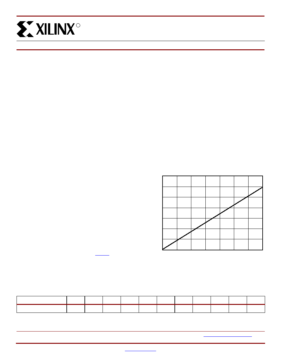
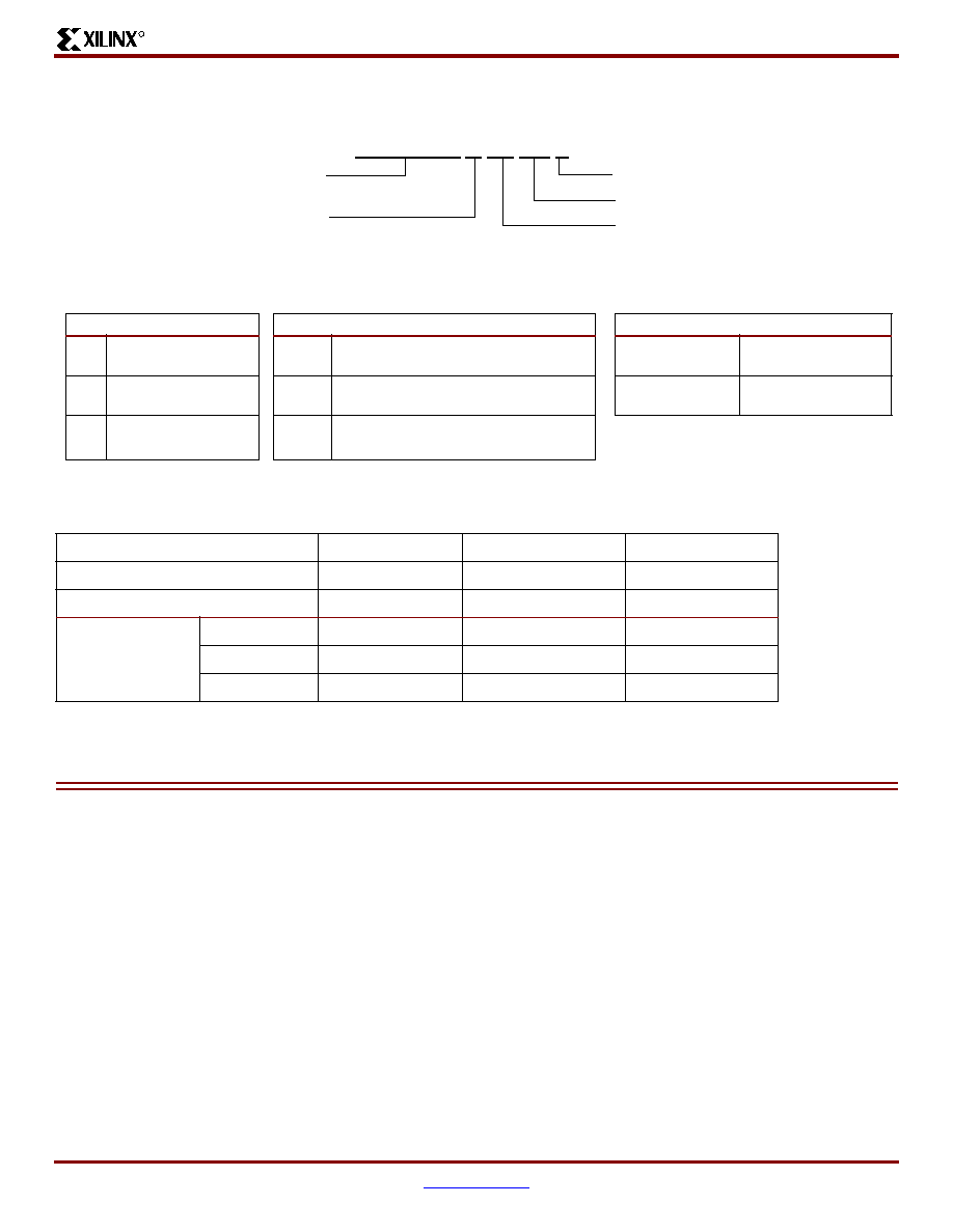
TotalCMOS Design Technique for Fast
Zero Power
Xilinx offers a TotalCMOS CPLD, both in process technol-
ogy and design technique. Xilinx employs a cascade of
CMOS gates to implement its sum of products instead of
the traditional sense amp approach. This CMOS gate imple-
mentation allows Xilinx to offer CPLDs that are both high
performance and low power, breaking the paradigm that to
have low power, you must have low performance. Refer to
Figure 1
and
Table 1
showing the I
CC
vs. Frequency of our
XCR3128XL TotalCMOS CPLD (data taken with eight
resetable up/down, 16-bit counters at 3.3V, 25
∞
C).
0
XCR3128XL 128 Macrocell CPLD
DS016 (v1.8) January 8, 2002
0
14
Preliminary Product Specification
R
Figure 1: Typical I
CC
vs. Frequency at V
CC
= 3.3V, 25
∞
C
Frequency (MHz)
DS016_01_112100
Typical I
CC
(mA)
0
0
10
20
30
50
70
40
60
120
140
100
80
60
40
20
Table 1: Typical I
CC
vs. Frequency at V
CC
= 3.3V, 25
∞
C
Frequency (MHz)
0
1
5
10
20
40
60
80
100
120
140
Typical I
CC
(mA)
0
0.5
2.2
4.4
8.7
17.1
25.3
33.6
41.6
49.7
57.7
XCR3128XL 128 Macrocell CPLD
2
www.xilinx.com
DS016 (v1.8) January 8, 2002
1-800-255-7778
Preliminary Product Specification
R
DC Electrical Characteristics Over Recommended Operating Conditions
(1)
Symbol
Parameter
Test Conditions
Min.
Max.
Unit
V
OH
(
2
)
Output High voltage
I
OH
= ≠8 mA
2.4
-
V
V
OL
Output Low voltage for 3.3V outputs
I
OL
= 8 mA
-
0.4
V
I
IL
Input leakage current
V
IN
= GND or V
CC
≠10
10
µ
A
I
IH
I/O High-Z leakage current
V
IN
= GND or V
CC
≠10
10
µ
A
I
CCSB
Standby current
V
CC
= 3.6V
-
100
µ
A
I
CC
Dynamic current
(
3
,
4
)
f = 1 MHz
-
1
mA
f = 50 MHz
-
30
mA
C
IN
Input pin capacitance
(
5
)
f = 1 MHz
-
8
pF
C
CLK
Clock input capacitance
(
5
)
f = 1 MHz
-
12
pF
C
I/O
I/O pin capacitance
(
5
)
f = 1 MHz
-
10
pF
Notes:
1.
See XPLA3 family data sheet (
DS012
) for recommended operating conditions.
2.
See
Figure 2
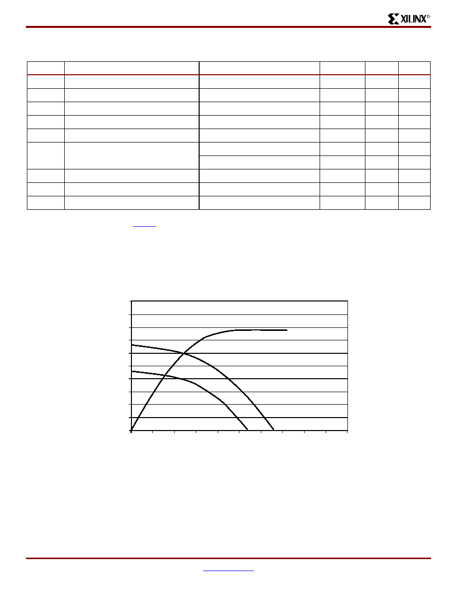
for output drive characteristics of the XPLA3 family.
3.
See
Table 1
, Figure1 for typical values.
4.
This parameter measured with a 16-bit, resetable up/down counter loaded into every function block, with all outputs disabled and
unloaded. Inputs are tied to V
CC
or ground. This parameter guaranteed by design and characterization, not testing.
5.
Typical values, not tested.
Figure 2: Typical I/V Curve for the XPLA3 Family
0
0
10
20
30
40
50
60
70
80
90
100
0.5
1
1.5
2
2.5
3
3.5
4
4.5
5
Volts
I
OL
(3.3V)
I
OH
(3.3V)
I
OH
(2.7V)
mA
DS012_10_041901
XCR3128XL 128 Macrocell CPLD
DS016 (v1.8) January 8, 2002
www.xilinx.com
3
Preliminary Product Specification
1-800-255-7778
R
AC Electrical Characteristics Over Recommended Operating Conditions
(1,2)
Symbol
Parameter
-6
-7
-10
Unit
Min.
Max.
Min.
Max.
Min.
Max.
T
PD1
Propagation delay time (single p-term)
-
5.5
-
7.0
-
9.1
ns
T
PD2
Propagation delay time (OR array)
(3)
-
6.0
-
7.5
-
10.0
ns
T
CO
Clock to output (global synchronous pin clock)
-
4.0
5.0
-
6.5
ns
T
SUF
Setup time (fast input register)
2.5
-
3.0
-
3.0
-
ns
T
SU1
(4)
Setup time (single p-term)
3.5
-
4.3
-
5.4
-
ns
T
SU2
Setup time (OR array)
4.0
-
4.8
-
6.3
-
ns
T
H
(4)
Hold time
0
-
0
-
0
-
ns
T
WLH
(4)
Global Clock pulse width (High or Low)
2.5
-
3.0
-
4.0
-
ns
Tt
PLH
(4)
P-term clock pulse width
4.0
-
5.0
-
6.0
-
ns
T
R
(4)
Input rise time
-
20
-
20
-
20
ns
T
L
(4)
Input fall time
-
20
-
20
-
20
ns
f
SYSTEM
(4)
Maximum system frequency
-
145
-
119
-
95
MHz
T
CONFIG
(4)
Configuration time
(5)
-
60
-
60
-
60
µ
s
T
INIT
(4)
ISP initialization time
-
60
-
60
-
60
µ
s
T
POE
(4)
P-term OE to output enabled
-
7.5
-
9.3
-
11.2
ns
T
POD
(4)
P-term OE to output disabled
(6)
-
7.5
-
9.3
-
11.2
ns
T
PCO
(4)
P-term clock to output
-
6.5
-
8.3
-
10.7
ns
T
PAO
(4)
P-term set/reset to output valid
-
8.0
-
9.3
-
11.2
ns
Advance
Preliminary
Notes:
1.
Specifications measured with one output switching.
2.
See XPLA3 family data sheet (
DS012
) for recommended operating conditions.
3.
See
Figure 4
for derating.
4.
These parameters guaranteed by design and/or characterization, not testing.
5.
Typical current draw during configuration is 9 mA at 3.6V.
6.
Output C
L
= 5 pF.
XCR3128XL 128 Macrocell CPLD
4
www.xilinx.com
DS016 (v1.8) January 8, 2002
1-800-255-7778
Preliminary Product Specification
R
Internal Timing Parameters
(1,2)
Symbol
Parameter
-6
-7
-10
Unit
Min.
(3)
Max.
(3)
Min.
Max.
Min.
Max.
Buffer Delays
T
IN
Input buffer delay
-
1.3
-
1.6
-
2.2
ns
T
FIN
Fast Input buffer delay
-
2.3
-
3.0
-
3.1
ns
T
GCK
Global Clock buffer delay
-
0.8
-
1.0
-
1.3
ns
T
OUT
Output buffer delay
-
2.2
-
2.7
-
3.6
ns
T
EN
Output buffer enable/disable delay
-
4.2
-
5.0
-
5.7
ns
Internal Register and Combinatorial Delays
T
LDI
Latch transparent delay
-
1.3
-
1.6
-
2.0
ns
T
SUI
Register setup time
1.0
-
1.0
-
1.2
-
ns
T
HI
Register hold time
0.3
-
0.5
-
0.7
-
ns
T
ECSU
Register clock enable setup time
2.0
-
2.5
-
3.0
-
ns
T
ECHO
Register clock enable hold time
3.0
-
4.5
-
5.5
-
ns
T
COI
Register clock to putput delay
-
1.0
-
1.3
-
1.6
ns
T
AOI
Register async. S/R to output delay
-
2.5
-
2.3
-
2.1
ns
T
RAI
Register async. recovery
-
4.0
-
5.0
-
6.0
ns
T
LOGI1
Internal logic delay (single p-term)
-
2.0
-
2.7
-
3.3
ns
T
LOGI2
Internal logic delay (PLA OR term)
-
2.5
-
3.2
-
4.2
ns
Feedback Delays
T
F
ZIA delay
-
1.7
-
2.1
-
3.0
ns
Time Adders
T
LOGI3
Fold-back NAND delay
-
6.0
-
7.5
-
9.5
ns
T
UDA
Universal delay
-
1.7
-
2.2
-
2.7
ns
T
SLEW
Slew rate limited delay
-
4.0
-
5.0
-
6.0
ns
Advance
Preliminary
Notes:
1.
These parameters guaranteed by design and/or characterization, not testing.
2.
See XPLA family data sheet (
DS012
) for timing model.
3.
Contact Xilinx for update on advance specification.
XCR3128XL 128 Macrocell CPLD
DS016 (v1.8) January 8, 2002
www.xilinx.com
5
Preliminary Product Specification
1-800-255-7778
R
Switching Characteristics
Figure 3: AC Load Circuit
DS016_03_102401
Component
Values
R1
390
R2
390
C1
35 pF
Measurement
S1
S2
T
POE (High)
T
POE (Low)
T
P
Open
Closed
Closed
Open
Closed
Closed
VCC
V
OUT
V
IN
C1
R1
R2
S1
S2
Note: For T
POD
, C1 = 5 pF. Delay measured at
output level of V
OL
+ 300 mV, V
OH
≠ 300 mV.
Figure 4: Derating Curve for T
PD2
5.6
5.8
6.0
6.2
6.4
6.6
6.8
7.2
7.0
7.4
1
2
4
8
DS016_04_042800
16
Number of Adjacent Outputs Switching
ns
Figure 5: Voltage Waveform
90%
10%
1.5 ns
1.5 ns
DS016_05_042800
+3.0V
0V
Measurements:
All circuit delays are measured at the +1.5V level of
inputs and outputs, unless otherwise specified.
T
R
T
L
XCR3128XL 128 Macrocell CPLD
6
www.xilinx.com
DS016 (v1.8) January 8, 2002
1-800-255-7778
Preliminary Product Specification
R
Pin Descriptions
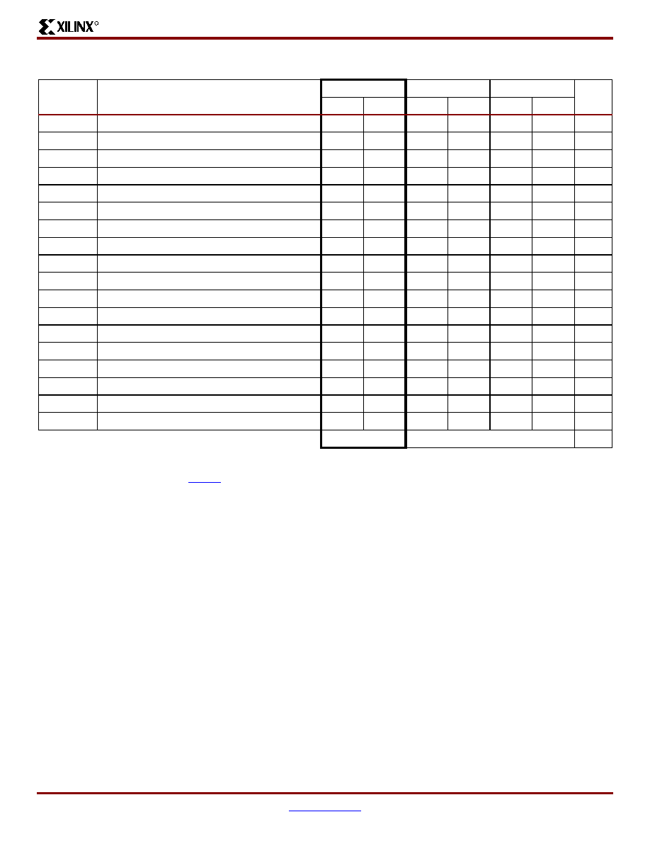
Table 2: XCR3128XL User I/O Pins
VQ100
CS144
TQ144
Total User I/O Pins
84
108
108
Table 3: XCR3128XL I/O Pins
Function
Block
Macrocell
VQ100
CS144
TQ144
1
1
-
B12
106
1
2
73
(1)
D11
(1)
104
(1)
1
3
72
D12
102
1
4
71
D13
101
1
5
70
E10
100
1
6
69
E11
99
1
7
68
E12
98
1
8
-
-
-
1
9
-
-
-
1
10
-
-
-
1
11
67
E13
97
1
12
-
F10
96
1
13
65
F12
94
1
14
64
F13
93
1
15
63
G10
92
1
16
-
G11
91
2
1
75
A13
107
2
2
76
A12
109
2
3
77
B11
110
2
4
78
A11
111
2
5
79
D10
112
2
6
80
C10
113
2
7
81
B10
114
2
8
-
-
-
2
9
-
-
-
2
10
-
-
-
2
11
83
D9
116
2
12
84
C9
117
2
13
85
B9
118
2
14
-
A9
119
2
15
-
D8
120
2
16
-
C8
121
3
1
-
G13
90
3
2
62
(1)
G12
(1)
89
(1)
3
3
61
H13
88
3
4
60
H12
87
3
5
-
H11
86
3
6
58
J13
84
3
7
57
J12
83
3
8
-
-
-
3
9
-
-
-
3
10
-
-
-
3
11
56
J11
82
3
12
55
J10
81
3
13
54
K13
80
3
14
53
K12
79
3
15
52
K11
78
3
16
-
K10
77
4
1
-
M8
60
4
2
40
L8
61
4
3
41
K8
62
4
4
42
N9
63
4
5
44
L9
65
4
6
45
K9
66
4
7
46
N10
67
4
8
-
-
-
4
9
-
-
-
4
10
-
-
-
4
11
47
M10
68
4
12
48
L10
69
4
13
49
N11
70
4
14
50
M11
71
4
15
-
L11
72
4
16
-
M12
74
5
1
2
A1
1
5
2
1
A2
143
5
3
100
C3
142
5
4
99
B3
141
5
5
98
A3
140
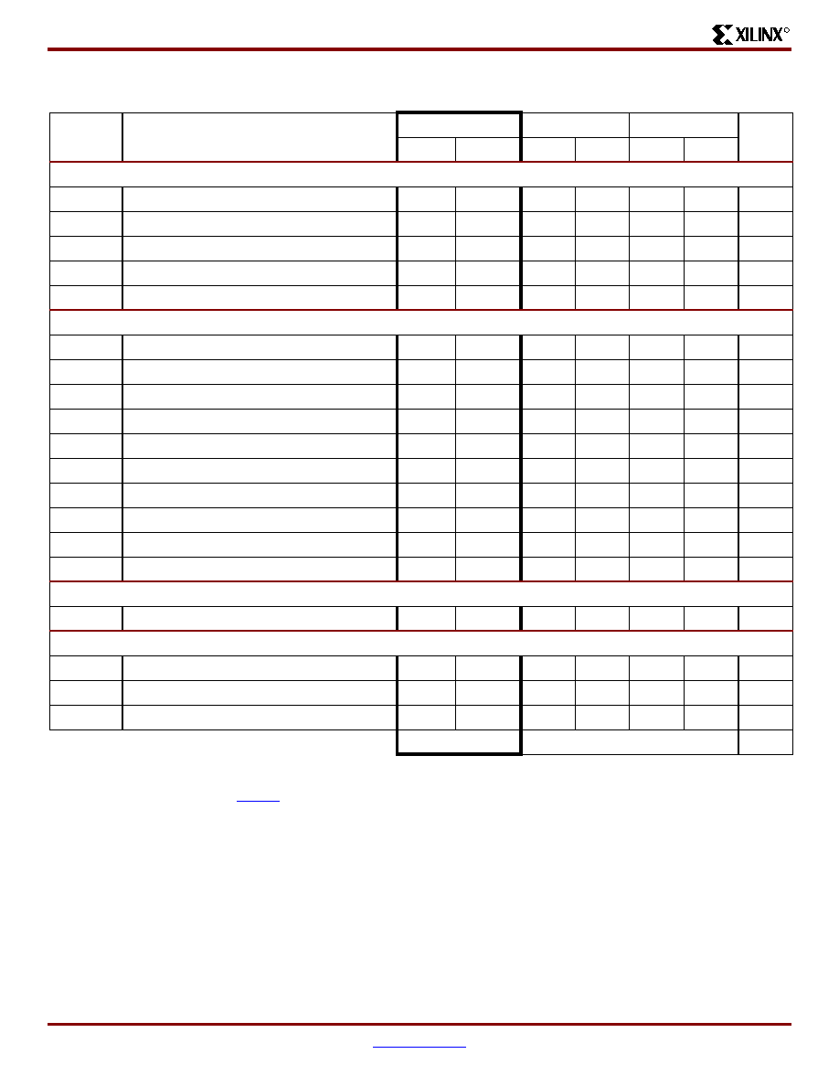
Table 3: XCR3128XL I/O Pins (Continued)
Function
Block
Macrocell
VQ100
CS144
TQ144
XCR3128XL 128 Macrocell CPLD
DS016 (v1.8) January 8, 2002
www.xilinx.com
7
Preliminary Product Specification
1-800-255-7778
R
5
6
97
C4
139
5
7
96
B4
138
5
8
-
-
-
5
9
-
-
-
5
10
-
-
-
5
11
-
A4
137
5
12
-
D5
136
5
13
94
B5
134
5
14
93
A5
133
5
15
92
D6
132
5
16
-
C6
131
6
1
-
B1
2
6
2
4
(1)
D2
(1)
4
(1)
6
3
5
D1
5
6
4
6
E4
6
6
5
7
E3
7
6
6
8
E2
8
6
7
9
E1
9
6
8
-
-
-
6
9
-
-
-
6
10
-
-
-
6
11
10
F4
10
6
12
-
F3
11
6
13
-
F2
12
6
14
12
G2
14
6
15
13
G1
15
6
16
14
G3
16
7
1
-
N7
56
7
2
37
M7
55
7
3
36
N6
54
7
4
35
M6
53
7
5
33
M5
46
7
6
32
L5
45
7
7
31
K5
44
7
8
-
-
-
7
9
-
-
-
7
10
-
-
-
Table 3: XCR3128XL I/O Pins (Continued)
Function
Block
Macrocell
VQ100
CS144
TQ144
7
11
30
N4
42
7
12
29
M4
41
7
13
28
L4
40
7
14
27
K4
39
7
15
-
N3
38
7
16
-
M3
37
8
1
-
H1
18
8
2
15
(1)
H2
(1)
20
(1)
8
3
16
H3
21
8
4
17
H4
22
8
5
-
J1
23
8
6
19
J3
25
8
7
20
J4
26
8
8
-
-
-
8
9
-
-
-
8
10
-
-
-
8
11
21
K1
27
8
12
22
K2
28
8
13
23
K3
29
8
14
24
L1
30
8
15
25
M2
31
8
16
-
N1
32
Notes:
1.
JTAG pins
Table 3: XCR3128XL I/O Pins (Continued)
Function
Block
Macrocell
VQ100
CS144
TQ144
XCR3128XL 128 Macrocell CPLD
8
www.xilinx.com
DS016 (v1.8) January 8, 2002
1-800-255-7778
Preliminary Product Specification
R
Table 4: XCR3128XL Global, JTAG, Port Enable, Power,
and No Connect Pins
Pin Type
VQ100
CS144
TQ144
IN0 / CLK0
90
D7
128
IN1 / CLK1
89
C7
127
IN2 / CLK2
88
A7
126
IN3 / CLK3
87
B7
125
TCK
62
G12
89
TDI
4
D2
4
TDO
73
D11
104
TMS
15
H2
20
PORT_EN
11
(1)
F1
(1)
13
(1)
Vcc
3, 18, 34,
39, 51, 66,
82, 91
A10, B2, B6,
B8, D4, F11,
J2, K6, K7,
L13, N5,
N12
24, 50, 51,
58, 73, 76,
95, 115,
123, 130,
144
GND
26, 38, 43,
59, 74, 86,
95
A6, A8, C5,
C13, D3,
G4, H10,
L6, L7, M9,
N2, N8
3, 17, 33,
52, 57, 59,
64, 85, 105,
124, 129,
135
No Connects
-
B13, C1,
C2, C11,
C12, L2, L3,
L12, M1,
M13, N13
19, 34, 35,
36, 43, 47,
48, 49, 75,
103, 108,
122
Notes:
1.
Port Enable is brought High to enable JTAG pins when JTAG
pins are used as I/O. See family data sheet (
DS012
) for full
explanation.
Table 4: XCR3128XL Global, JTAG, Port Enable, Power,
and No Connect Pins
Pin Type
VQ100
CS144
TQ144
XCR3128XL 128 Macrocell CPLD
DS016 (v1.8) January 8, 2002
www.xilinx.com
9
Preliminary Product Specification
1-800-255-7778
R
Ordering Information
Component Availability
XCR3128XL -7 VQ 100 C
Example:
Temperature Range
Number of Pins
Package Type
Device Type
Speed Grade
Device Ordering Options
Speed Package
Temperature
-10
10 ns pin-to-pin delay
VQ100
100-pin Very Thin Quad Flat Package
C = Commercial
T
A
= 0∞C to +70∞C
V
CC
= 3.0V to 3.6V
-7
7.5 ns pin-to-pin delay
CS144
144-ball Chip Scale Package
I = Industrial
T
A
= ≠40∞C to +85∞C
V
CC
= 2.7V to 3.6V
-6
6 ns pin-to-pin delay
TQ144
144-pin Thin Quad Flat Pack
Pins
100
144
144
Type
Plastic VQFP
Plastic TQFP
Plastic BGA
Code
VQ100
TQ144
CS144
XCR3128XL
-6
(C)
(C)
(C)
-7
C, (I)
C, (I)
C, (I)
-10
C,I
C,I
C,I
Notes:
1.
Parenthesis indicate future planned products. Please contact Xilinx for up-to-date information.
XCR3128XL 128 Macrocell CPLD
10
www.xilinx.com
DS016 (v1.8) January 8, 2002
1-800-255-7778
Preliminary Product Specification
R
Revision History
The following table shows the revision history for this document.
Date
Version
Revision
04/07/00
1.0
Initial Xilinx release.
05/03/00
1.1
Minor updates and added Boundary Scan to pinout table.
11/20/00
1.2
Updated pinout tables; corrected note in
Table 4
to read: "port enable pin is brought High".
12/08/00
1.3
Updated pinout tables.
01/17/01
1.4
Removed Timing Model.
04/11/01
1.5
Added Typical I/V curve,
Figure 2
; added
Table 2
: Total User I/O; changed V
OH
spec.
04/19/01
1.6
Updated Typical I/V curve,
Figure 2
: added voltage levels.
08/10/01
1.7
Moved
Figure 1
and
Table 1
to first page. Changed VQ144 to VQ100 in
Table 2
.
01/08/02
1.8
Updated T
SUF
and T
FIN
spec to match software timing. Added single p-term setup time
(T
SU1
) to AC Table, renamed T
SU
to T
SU2
for setup time through the OR array. Added T
INIT
spec. Updated T
CONFIG
spec. Updated T
HI
spec to correct a typo. Updated AC Load Circuit
diagram to more closely resemble true test conditions, added note for T
POD
delay
measurement.