DS013 (v1.2) May 3, 2000
www.xilinx.com
1
Preliminary Product Specification
1-800-255-7778
© 2000 Xilinx, Inc. All rights reserved. All Xilinx trademarks, registered trademarks, patents, and disclaimers are as listed at
http://www.xilinx.com/legal.htm
. All other trademarks and registered trademarks are the property of their respective owners.
All specifications are subject to change without notice.
Features
∑
7.5 ns pin-to-pin logic delays
∑
System frequencies up to 140 MHz
∑
256 macrocells with 6,000 usable gates
∑
Available in small footprint packages
-
144-pin TQFP (116 user I/O pins)
-
208-pin PQFP (160 user I/O)
-
280-ball CS BGA (160 user I/O)
∑
Optimized for 3.3V systems
-
Ultra low power operation
-
5V tolerant I/O pins with 3.3V core supply
-
Advanced 0.35 micron five metal layer re-
programmable process
-
FZPTM CMOS design technology
∑
Advanced system features
-
In-system programming
-
Input registers
-
Predictable timing model
-
Up to 23 clocks available per logic block
-
Excellent pin retention during design changes
-
Full IEEE Standard 1149.1 boundary-scan (JTAG)
-
Four global clocks
-
Eight product term control terms per logic block
∑
Fast ISP programming times
∑
Port Enable pin for additional I/O
∑
2.7V to 3.6V industrial grade voltage range
∑
Programmable slew rate control per output
∑
Security bit prevents unauthorized access
∑
Refer to XPLA3 family data sheet (DS012) for
architecture description
Description
The XCR3256XL is a 3.3V, 256 macrocell CPLD targeted at
power sensitive designs that require leading edge program-
mable logic solutions. A total of 16 logic blocks provide
6,000 usable gates. Pin-to-pin propagation delays are
7.5 ns with a maximum system frequency of 140 MHz.
TotalCMOSTM Design Technique for
Fast Zero Power
Xilinx offers a TotalCMOS CPLD, both in process technol-
ogy and design technique. Xilinx employs a cascade of
CMOS gates to implement its sum of products instead of
the traditional sense amp approach. This CMOS gate
implementation allows Xilinx to offer CPLDs that are both
high performance and low power, breaking the paradigm
that to have low power, you must have low performance.
Refer to
Figure 1
and
Table 1
showing the I
CC
vs. Fre-
quency of our XCR3256XL TotalCMOS CPLD (data taken
with 16 up/down, loadable 16-bit counters at 3.3V, 25
∞
C).
0
XCR3256XL 256 Macrocell CPLD
DS013 (v1.2) May 3, 2000
0
14
Preliminary Product Specification
R

XCR3256XL 256 Macrocell CPLD
2
www.xilinx.com
DS013 (v1.2) May 3, 2000
1-800-255-7778
Preliminary Product Specification
R
DC Electrical Characteristics Over Recommended Operating Conditions
(1)
Figure 1: XCR3256XL Typical I
CC
vs. Frequency at V
CC
= 3.3V, 25
∞
C
Table 1: Typical I
CC
vs. Frequency at V
CC
= 3.3V, 25
∞
C
Frequency (MHz)
0
1
10
20
40
60
80
100
120
140
Typical I
CC
(mA)
0.02
0.91
8.87
17.7
34.8
51.5
68
84.2
100.1
116.6
Symbol
Parameter
Test Conditions
Min.
Max.
Unit
V
OH
Output High voltage for 3.3V outputs
I
OH
= ≠8 mA
2.4
-
V
V
OL
Output Low voltage for 3.3V outputs
I
OL
= 8 mA
-
0.4
V
I
IL
Input leakage current
V
IN
= GND or V
CC
≠10
10
m
A
I
IH
I/O High-Z leakage current
V
IN
= GND or V
CC
≠10
10
m
A
I
CCSB
Standby current
V
CC
= 3.6V
-
100
m
A
I
CC
Dynamic current
(2,3)
f = 1 MHz
-
2
mA
f = 50 MHz
-
60
mA
C
IN
Input pin capacitance
(4)
f = 1 MHz
-
8
pF
C
CLK
Clock input capacitance
(4)
f = 1 MHz
5
12
pF
C
I/O
I/O pin capacitance
(4)
f = 1 MHz
-
10
pF
Notes:
1.
See XPLA3 family data sheet (DS012) for recommended operating conditions.
2.
See
Table 1
, Figure1 for typical values.
3.
This parameter measured with a 16-bit, loadable up/down counter loaded into every logic block, with all outputs disabled and
unloaded. Inputs are tied to V
CC
or ground. This parameter guaranteed by design and characterization, not testing.
4.
Typical values not tested.
0
20
40
60
80
100
120
140
0
20
40
60
80
100
120
140
160
Frequency (MHz)
Typical ICC (mA)

XCR3256XL 256 Macrocell CPLD
DS013 (v1.2) May 3, 2000
www.xilinx.com
3
Preliminary Product Specification
1-800-255-7778
R
AC Electrical Characteristics Over Recommended Operating Conditions
(1,2)
Symbol
Parameter
-7
-10
-12
Unit
Min.
Max.
Min.
Max.
Min.
Max.
T
PD1
Propagation delay time (single p-term)
-
7.0
-
9.0
-
10.8
ns
T
PD2
Propagation delay time (OR array)
(3)
-
7.5
-
10.0
-
12.0
ns
T
CO
Clock to output (global synchronous pin clock)
-
4.5
-
5.8
-
6.9
ns
T
SUF
Setup time fast
2.0
-
2.5
-
3.0
-
ns
T
SU
Setup time
4.8
-
6.5
-
7.9
-
ns
T
H
Hold time
0
-
0
-
0
-
ns
T
WLH
Global clock pulse width (High or Low)
3.0
-
4.0
-
5.0
-
ns
T
PLH
P-term clock pulse width (High or Low)
4.5
-
6.0
-
7.5
-
ns
T
R
Input rise time
-
20
-
20
-
20
ns
T
L
Input fall time
-
20
-
20
-
20
ns
f
SYSTEM
Maximum system frequency
-
140
-
105
-
88
MHz
T
CONFIG
Configuration time
(4)
-
40
-
40
-
40
m
s
T
POE
P-term OE to output enabled
-
9.0
-
11.0
-
13.0
ns
T
POD
P-term OE to output disabled
(5)
-
9.0
-
11.0
-
13.0
ns
T
PCO
P-term clock to output
-
8.0
-
10.3
-
12.4
ns
T
PAO
P-term set/reset to output valid
-
9.0
-
11.0
-
13.0
ns
Notes:
1.
Specifications measured with one output switching.
2.
See XPLA3 Family Data Sheet (DS012) for recommended operating conditions.
3.
See
Figure 4
for derating.
4.
Typical current draw during configuration is 10 mA at 3.6V.
5.
Output C
L
= 5 pF.
XCR3256XL 256 Macrocell CPLD
4
www.xilinx.com
DS013 (v1.2) May 3, 2000
1-800-255-7778
Preliminary Product Specification
R
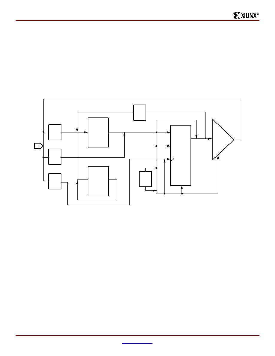
Timing Model
The XPLA3 architecture follows a simple timing model that
allows deterministic timing in design and redesign. The
basic timing model is shown in
Figure 2
. One key feature of
the XPLA3 CPLD is the ability to have up to 48 product term
inputs into a single macrocell and maintain consistent tim-
ing. This is achieved through the use of a fully populated
PLA (Programmable AND Programmable OR Array) which
also has the ability to share product terms and only use the
required amount of product terms per macrocell. There is a
fast path (T
LOGI1
) into the macrocell which is used if there is
a single product term. The T
LOGI2
path is used for multiple
product term timing. For optimization of logic, the XPLA3
CPLD architecture includes a Fold-back NAND path
(T
LOGI3
). There is a fast input path to each macrocell if used
as an Input Register (T
FIN
). XPLA3 also includes universal
control terms (T
UDA
) that can be used for synchronization of
the macrocell registers in different logic blocks. There is
also slew rate control and output enable control on a per
macrocell basis.
Figure 2: XPLA3 Timing Model
T
IN
T
F
T
OUT
T
EN
T
SLEW
T
LOGI1,2
DLT
Q
CE
S/R
T
LOGI3
T
FIN
T
GCK
T
UDA
DS017_02_042800
XCR3256XL 256 Macrocell CPLD
DS013 (v1.2) May 3, 2000
www.xilinx.com
5
Preliminary Product Specification
1-800-255-7778
R
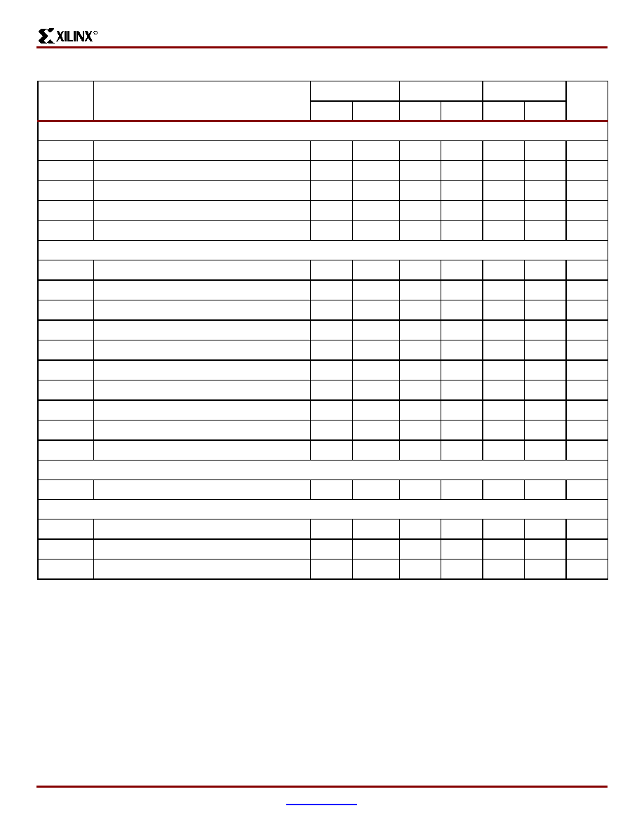
Internal Timing Parameters
Symbol
Parameter
-7
-10
-12
Unit
Min.
Max.
Min.
Max.
Min.
Max.
Buffer Delays
T
IN
Input buffer delay
-
2.5
-
3.3
-
4.0
ns
T
FIN
Fast input buffer delay
-
2.2
-
2.8
-
3.3
ns
T
GCK
Global clock buffer delay
-
1.0
-
1.3
-
1.5
ns
T
OUT
Output buffer delay
-
2.5
-
2.8
-
3.3
ns
T
EN
Output buffer enable/disable delay
-
4.5
-
5.2
-
6.0
ns
Internal Register and Combinatorial Delays
T
LDI
Latch transparent delay
-
1.3
-
1.6
-
2.0
ns
T
SUI
Register setup time
0.8
-
1.0
-
1.2
-
ns
T
HI
Register hold time
4.0
-
5.5
-
6.7
-
ns
T
ECSU
Register clock enable setup time
2.0
-
2.5
-
3.0
-
ns
T
ECHO
Register clock enable hold time
3.0
-
4.5
-
5.5
-
ns
T
COI
Register clock to output delay
-
1.0
-
1.3
-
1.6
ns
T
AOI
Register async. S/R to output delay
-
2.0
-
2.0
-
2.2
ns
T
RAI
Register async. recovery
-
5.0
-
7.0
-
8.0
ns
T
LOGI1
Internal logic delay (single p-term)
-
2.0
-
2.5
-
3.0
ns
T
LOGI2
Internal logic delay (PLA OR term)
-
2.5
-
3.5
-
4.2
ns
Feedback Delays
T
F
ZIA delay
-
2.8
-
3.7
-
4.4
ns
Time Adders
T
LOGI3
Fold-back NAND delay
-
6.0
-
8.0
-
9.5
ns
T
UDA
Universal delay
-
2.0
-
2.5
-
3.0
ns
T
SLEW
Slew rate limited delay
-
4.0
-
5.0
-
6.0
ns