© 2001 Xilinx, Inc. All rights reserved. All Xilinx trademarks, registered trademarks, patents, and disclaimers are as listed at
http://www.xilinx.com/legal.htm
.
All other trademarks and registered trademarks are the property of their respective owners. All specifications are subject to change without notice.
DS003-1 (v2.5 ) April 2, 2001
www.xilinx.com
Module 1 of 4
Product Specification
1-800-255-7778
1
Features
∑
Fast, high-density Field-Programmable Gate Arrays
-
Densities from 50k to 1M system gates
-
System performance up to 200 MHz
-
66-MHz PCI Compliant
-
Hot-swappable for Compact PCI
∑
Multi-standard SelectIOTM interfaces
-
16 high-performance interface standards
-
Connects directly to ZBTRAM devices
∑
Built-in clock-management circuitry
-
Four dedicated delay-locked loops (DLLs) for
advanced clock control
-
Four primary low-skew global clock distribution
nets, plus 24 secondary local clock nets
∑
Hierarchical memory system
-
LUTs configurable as 16-bit RAM, 32-bit RAM,
16-bit dual-ported RAM, or 16-bit Shift Register
-
Configurable synchronous dual-ported 4k-bit
RAMs
-
Fast interfaces to external high-performance RAMs
∑
Flexible architecture that balances speed and density
-
Dedicated carry logic for high-speed arithmetic
-
Dedicated multiplier support
-
Cascade chain for wide-input functions
-
Abundant registers/latches with clock enable, and
dual synchronous/asynchronous set and reset
-
Internal 3-state bussing
-
IEEE 1149.1 boundary-scan logic
-
Die-temperature sensor diode
∑
Supported by FPGA FoundationTM and Alliance
Development Systems
-
Complete support for Unified Libraries, Relationally
Placed Macros, and Design Manager
-
Wide selection of PC and workstation platforms
∑
SRAM-based in-system configuration
-
Unlimited re-programmability
-
Four programming modes
∑
0.22
m
m 5-layer metal process
∑
100% factory tested
Description
The Virtex FPGA family delivers high-performance,
high-capacity programmable logic solutions. Dramatic
increases in silicon efficiency result from optimizing the new
architecture for place-and-route efficiency and exploiting an
aggressive 5-layer-metal 0.22
m
m CMOS process. These
advances make Virtex FPGAs powerful and flexible alterna-
tives to mask-programmed gate arrays. The Virtex family
comprises the nine members shown in
Table 1
.
Building on experience gained from previous generations of
FPGAs, the Virtex family represents a revolutionary step
forward in programmable logic design. Combining a wide
variety of programmable system features, a rich hierarchy of
fast, flexible interconnect resources, and advanced process
technology, the Virtex family delivers a high-speed and
high-capacity programmable logic solution that enhances
design flexibility while reducing time-to-market.
0
VirtexTM 2.5 V
Field Programmable Gate Arrays
DS003-1 (v2.5 ) April 2, 2001
0
3
Product Specification
R
Table 1: Virtex Field-Programmable Gate Array Family Members
Device
System Gates
CLB Array
Logic Cells
Maximum
Available I/O
Block RAM
Bits
Maximum
SelectRAM+TM Bits
XCV50
57,906
16x24
1,728
180
32,768
24,576
XCV100
108,904
20x30
2,700
180
40,960
38,400
XCV150
164,674
24x36
3,888
260
49,152
55,296
XCV200
236,666
28x42
5,292
284
57,344
75,264
XCV300
322,970
32x48
6,912
316
65,536
98,304
XCV400
468,252
40x60
10,800
404
81,920
153,600
XCV600
661,111
48x72
15,552
512
98,304
221,184
XCV800
888,439
56x84
21,168
512
114,688
301,056
XCV1000
1,124,022
64x96
27,648
512
131,072
393,216
VirtexTM 2.5 V Field Programmable Gate Arrays
R
Module 1 of 4
www.xilinx.com
DS003-1 (v2.5 ) April 2, 2001
2
1-800-255-7778
Product Specification
Virtex Architecture
Virtex devices feature a flexible, regular architecture that
comprises an array of configurable logic blocks (CLBs) sur-
rounded by programmable input/output blocks (IOBs), all
interconnected by a rich hierarchy of fast, versatile routing
resources. The abundance of routing resources permits the
Virtex family to accommodate even the largest and most
complex designs.
Virtex FPGAs are SRAM-based, and are customized by
loading configuration data into internal memory cells. In
some modes, the FPGA reads its own configuration data
from an external PROM (master serial mode). Otherwise,
the configuration data is written into the FPGA (Select-
MAPTM, slave serial, and JTAG modes).
The standard Xilinx FoundationTM and Alliance SeriesTM
Development systems deliver complete design support for
Virtex, covering every aspect from behavioral and sche-
matic entry, through simulation, automatic design transla-
tion and implementation, to the creation, downloading, and
readback of a configuration bit stream.
Higher Performance
Virtex devices provide better performance than previous
generations of FPGA. Designs can achieve synchronous
system clock rates up to 200 MHz including I/O. Virtex
inputs and outputs comply fully with PCI specifications, and
interfaces can be implemented that operate at 33 MHz or 66
MHz. Additionally, Virtex supports the hot-swapping
requirements of Compact PCI.
Xilinx thoroughly benchmarked the Virtex family. While per-
formance is design-dependent, many designs operated
internally at speeds in excess of 100 MHz and can achieve
200 MHz.
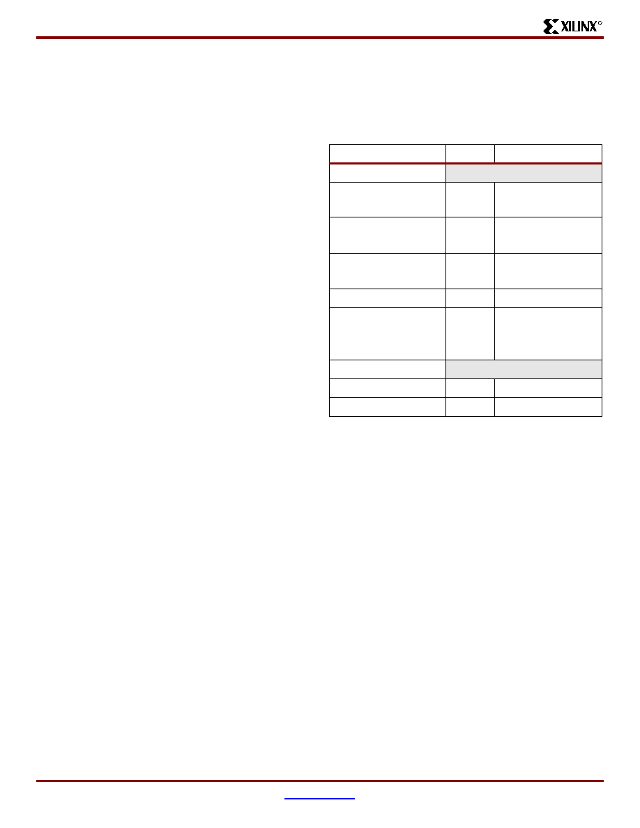
Table 2
shows performance data for representa-
tive circuits, using worst-case timing parameters.
Table 2: Performance for Common Circuit Functions
Function
Bits
Virtex -6
Register-to-Register
Adder
16
64
5.0 ns
7.2 ns
Pipelined Multiplier
8 x 8
16 x 16
5.1 ns
6.0 ns
Address Decoder
16
64
4.4 ns
6.4 ns
16:1 Multiplexer
5.4 ns
Parity Tree
9
18
36
4.1 ns
5.0 ns
6.9 ns
Chip-to-Chip
HSTL Class IV
200 MHz
LVTTL,16mA, fast slew
180 MHz
VirtexTM 2.5 V Field Programmable Gate Arrays
R
DS003-1 (v2.5 ) April 2, 2001
www.xilinx.com
Module 1 of 4
Product Specification
1-800-255-7778
3
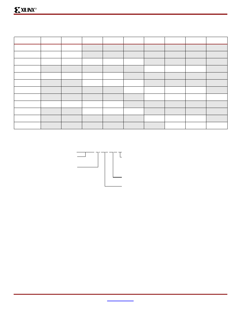
Virtex Device/Package Combinations and Maximum I/O
Virtex Ordering Information
Table 3: Virtex Family Maximum User I/O by Device/Package (Excluding Dedicated Clock Pins)
Package
XCV50
XCV100
XCV150
XCV200
XCV300
XCV400
XCV600
XCV800
XCV1000
CS144
94
94
TQ144
98
98
PQ240
166
166
166
166
166
HQ240
166
166
166
BG256
180
180
180
180
BG352
260
260
260
BG432
316
316
316
316
BG560
404
404
404
404
FG256
176
176
176
176
FG456
260
284
312
FG676
404
444
444
FG680
512
512
512
Figure 1: Virtex Ordering Information
XCV300 -6 PQ 240 C
Example:
Temperature Range
C = Commercial (T
J
= 0
∞
C to +85
∞
C)
I = Industrial (T
J
= ≠40
∞
C to +100
∞
C)
Number of Pins
Device Type
Speed Grade
-4
-5
-6
Package Type
BG = Ball Grid Array
FG = Fine-pitch Ball Grid Array
PQ = Plastic Quad Flat Pack
HQ = High Heat Dissipation QFP
TQ = Thin Quad Flat Pack
CS = Chip-scale Package
VirtexTM 2.5 V Field Programmable Gate Arrays
R
Module 1 of 4
www.xilinx.com
DS003-1 (v2.5 ) April 2, 2001
4
1-800-255-7778
Product Specification
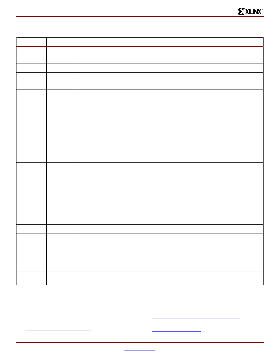
Revision History
Virtex Data Sheet
The Virtex Data Sheet contains the following modules:
∑
DS003-1, Virtex 2.5V FPGAs:
Introduction and Ordering Information (Module 1)
∑
DS003-2, Virtex 2.5V FPGAs:
Functional Description (Module 2)
∑
DS003-3, Virtex 2.5V FPGAs:
DC and Switching Characteristics (Module 3)
∑
DS003-4, Virtex 2.5V FPGAs:
Pinout Tables (Module 4)
Date
Version
Revision
11/98
1.0
Initial Xilinx release.
01/99
1.2
Updated package drawings and specs.
02/99
1.3
Update of package drawings, updated specifications.
05/99
1.4
Addition of package drawings and specifications.
05/99
1.5
Replaced FG 676 & FG680 package drawings.
07/99
1.6
Changed Boundary Scan Information and changed Figure 11, Boundary Scan Bit
Sequence. Updated IOB Input & Output delays. Added Capacitance info for different I/O
Standards. Added 5 V tolerant information. Added DLL Parameters and waveforms and
new Pin-to-pin Input and Output Parameter tables for Global Clock Input to Output and
Setup and Hold. Changed Configuration Information including Figures 12, 14, 17 & 19.
Added device-dependent listings for quiescent currents ICCINTQ and ICCOQ. Updated
IOB Input and Output Delays based on default standard of LVTTL, 12 mA, Fast Slew Rate.
Added IOB Input Switching Characteristics Standard Adjustments.
09/99
1.7
Speed grade update to preliminary status, Power-on specification and Clock-to-Out
Minimums additions, "0" hold time listing explanation, quiescent current listing update, and
Figure 6 ADDRA input label correction. Added T
IJITCC
parameter, changed T
OJIT
to
T
OPHASE
.
01/00
1.8
Update to speed.txt file 1.96. Corrections for CRs 111036,111137, 112697, 115479,
117153, 117154, and 117612. Modified notes for Recommended Operating Conditions
(voltage and temperature). Changed Bank information for V
CCO
in CS144 package on p.43.
01/00
1.9
Updated DLL Jitter Parameter table and waveforms, added Delay Measurement
Methodology table for different I/O standards, changed buffered Hex line info and
Input/Output Timing measurement notes.
03/00
2.0
New TBCKO values; corrected FG680 package connection drawing; new note about status
of CCLK pin after configuration.
05/00
2.1
Modified "Pins not listed ..." statement. Speed grade update to Final status.
05/00
2.2
Modified Table 18.
09/00
2.3
∑
Added XCV400 values to table under Minimum Clock-to-Out for Virtex Devices.
∑
Corrected Units column in table under IOB Input Switching Characteristics.
∑
Added values to table under CLB SelectRAM Switching Characteristics.
10/00
2.4
∑
Corrected Pinout information for devices in the BG256, BG432, and BG560 packages in
Table 18.
∑
Corrected BG256 Pin Function Diagram.
04/01
2.5
∑
Revised minimums for Global Clock Set-Up and Hold for LVTTL Standard, with DLL.
∑
Converted file to modularized format. See
Virtex Data Sheet
section.