
© 2000-2002 Xilinx, Inc. All rights reserved. All Xilinx trademarks, registered trademarks, patents, and disclaimers are as listed at
http://www.xilinx.com/legal.htm
.
All other trademarks and registered trademarks are the property of their respective owners. All specifications are subject to change without notice.
DS022-1 (v2.3) July 17, 2002
www.xilinx.com
Module 1 of 4
Production Product Specification
1-800-255-7778
1
Features
∑
Fast, High-Density 1.8 V FPGA Family
-
Densities from 58 k to 4 M system gates
-
130 MHz internal performance (four LUT levels)
-
Designed for low-power operation
-
PCI compliant 3.3 V, 32/64-bit, 33/ 66-MHz
∑
Highly Flexible SelectI/O+TM Technology
-
Supports 20 high-performance interface standards
-
Up to 804 singled-ended I/Os or 344 differential I/O
pairs for an aggregate bandwidth of > 100 Gb/s
∑
Differential Signalling Support
-
LVDS (622 Mb/s), BLVDS (Bus LVDS), LVPECL
-
Differential I/O signals can be input, output, or I/O
-
Compatible with standard differential devices
-
LVPECL and LVDS clock inputs for 300+ MHz
clocks
∑
Proprietary High-Performance SelectLinkTM
Technology
-
Double Data Rate (DDR) to Virtex-E link
-
Web-based HDL generation methodology
∑
Sophisticated SelectRAM+TM Memory Hierarchy
-
1 Mb of internal configurable distributed RAM
-
Up to 832 Kb of synchronous internal block RAM
-
True Dual-Port BlockRAM capability
-
Memory bandwidth up to 1.66 Tb/s (equivalent
bandwidth of over 100 RAMBUS channels)
-
Designed for high-performance Interfaces to
External Memories
-
200 MHz ZBT* SRAMs
-
200 Mb/s DDR SDRAMs
-
Supported by free Synthesizable reference design
∑
High-Performance Built-In Clock Management Circuitry
-
Eight fully digital Delay-Locked Loops (DLLs)
-
Digitally-Synthesized 50% duty cycle for Double
Data Rate (DDR) Applications
-
Clock Multiply and Divide
-
Zero-delay conversion of high-speed LVPECL/LVDS
clocks to any I/O standard
∑
Flexible Architecture Balances Speed and Density
-
Dedicated carry logic for high-speed arithmetic
-
Dedicated multiplier support
-
Cascade chain for wide-input function
-
Abundant registers/latches with clock enable, and
dual synchronous/asynchronous set and reset
-
Internal 3-state bussing
-
IEEE 1149.1 boundary-scan logic
-
Die-temperature sensor diode
∑
Supported by Xilinx FoundationTM and Alliance SeriesTM
Development Systems
-
Further compile time reduction of 50%
-
Internet Team Design (ITD) tool ideal for
million-plus gate density designs
-
Wide selection of PC and workstation platforms
∑
SRAM-Based In-System Configuration
-
Unlimited re-programmability
∑
Advanced Packaging Options
-
0.8 mm Chip-scale
-
1.0 mm BGA
-
1.27 mm BGA
-
HQ/PQ
∑
0.18
µm 6-Layer Metal Process
∑
100% Factory Tested
* ZBT is a trademark of Integrated Device Technology, Inc.
0
VirtexTM-E 1.8 V
Field Programmable Gate Arrays
DS022-1 (v2.3) July 17, 2002
0
0
Production Product Specification
R
VirtexTM-E 1.8 V Field Programmable Gate Arrays
R
Module 1 of 4
www.xilinx.com
DS022-1 (v2.3) July 17, 2002
2
1-800-255-7778
Production Product Specification
Virtex-E Compared to Virtex Devices
The Virtex-E family offers up to 43,200 logic cells in devices
up to 30% faster than the Virtex family.
I/O performance is increased to 622 Mb/s using Source
Synchronous data transmission architectures and synchro-
nous system performance up to 240 MHz using sin-
gled-ended SelectI/O technology. Additional I/O standards
are supported, notably LVPECL, LVDS, and BLVDS, which
use two pins per signal. Almost all signal pins can be used
for these new standards.
Virtex-E devices have up to 640 Kb of faster (250 MHz)
block SelectRAM, but the individual RAMs are the same
size and structure as in the Virtex family. They also have
eight DLLs instead of the four in Virtex devices. Each indi-
vidual DLL is slightly improved with easier clock mirroring
and 4x frequency multiplication.
V
CCINT
, the supply voltage for the internal logic and mem-
ory, is 1.8 V, instead of 2.5 V for Virtex devices. Advanced
processing and 0.18
µm design rules have resulted in
smaller dice, faster speed, and lower power consumption.
I/O pins are 3 V tolerant, and can be 5 V tolerant with an
external 100
resistor. PCI 5 V is not supported. With the
addition of appropriate external resistors, any pin can toler-
ate any voltage desired.
Banking rules are different. With Virtex devices, all input
buffers are powered by V
CCINT
. With Virtex-E devices, the
LVTTL, LVCMOS2, and PCI input buffers are powered by
the I/O supply voltage V
CCO
.
The Virtex-E family is not bitstream-compatible with the Vir-
tex family, but Virtex designs can be compiled into equiva-
lent Virtex-E devices.
The same device in the same package for the Virtex-E and
Virtex families are pin-compatible with some minor excep-
tions. See the data sheet pinout section for details.
General Description
The Virtex-E FPGA family delivers high-performance,
high-capacity programmable logic solutions. Dramatic
increases in silicon efficiency result from optimizing the new
architecture for place-and-route efficiency and exploiting an
aggressive 6-layer metal 0.18
µm CMOS process. These
advances make Virtex-E FPGAs powerful and flexible alter-
natives to mask-programmed gate arrays. The Virtex-E fam-
ily includes the nine members in
Table 1
.
Building on experience gained from Virtex FPGAs, the
Virtex-E family is an evolutionary step forward in program-
mable logic design. Combining a wide variety of program-
mable system features, a rich hierarchy of fast, flexible
interconnect resources, and advanced process technology,
the Virtex-E family delivers a high-speed and high-capacity
programmable logic solution that enhances design flexibility
while reducing time-to-market.
Virtex-E Architecture
Virtex-E devices feature a flexible, regular architecture that
comprises an array of configurable logic blocks (CLBs) sur-
rounded by programmable input/output blocks (IOBs), all
interconnected by a rich hierarchy of fast, versatile routing
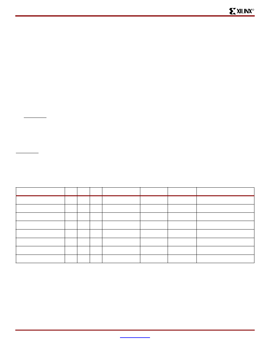
Table 1: Virtex-E Field-Programmable Gate Array Family Members
Device
System
Gates
Logic
Gates
CLB
Array
Logic
Cells
Differential
I/O Pairs
User
I/O
BlockRAM
Bits
Distributed
RAM Bits
XCV50E
71,693
20,736
16 x 24
1,728
83
176
65,536
24,576
XCV100E
128,236
32,400
20 x 30
2,700
83
196
81,920
38,400
XCV200E
306,393
63,504
28 x 42
5,292
119
284
114,688
75,264
XCV300E
411,955
82,944
32 x 48
6,912
137
316
131,072
98,304
XCV400E
569,952
129,600
40 x 60
10,800
183
404
163,840
153,600
XCV600E
985,882
186,624
48 x 72
15,552
247
512
294,912
221,184
XCV1000E
1,569,178
331,776
64 x 96
27,648
281
660
393,216
393,216
XCV1600E
2,188,742
419,904
72 x 108
34,992
344
724
589,824
497,664
XCV2000E
2,541,952
518,400
80 x 120
43,200
344
804
655,360
614,400
XCV2600E
3,263,755
685,584
92 x 138
57,132
344
804
753,664
812,544
XCV3200E
4,074,387
876,096
104 x 156
73,008
344
804
851,968
1,038,336

VirtexTM-E 1.8 V Field Programmable Gate Arrays
R
DS022-1 (v2.3) July 17, 2002
www.xilinx.com
Module 1 of 4
Production Product Specification
1-800-255-7778
3
resources. The abundance of routing resources permits the
Virtex-E family to accommodate even the largest and most
complex designs.
Virtex-E FPGAs are SRAM-based, and are customized by
loading configuration data into internal memory cells. Con-
figuration data can be read from an external SPROM (mas-
ter serial mode), or can be written into the FPGA
(SelectMAPTM, slave serial, and JTAG modes).
The standard Xilinx Foundation SeriesTM and Alliance
SeriesTM Development systems deliver complete design
support for Virtex-E, covering every aspect from behavioral
and schematic entry, through simulation, automatic design
translation and implementation, to the creation and down-
loading of a configuration bit stream.
Higher Performance
Virtex-E devices provide better performance than previous
generations of FPGAs. Designs can achieve synchronous
system clock rates up to 240 MHz including I/O or 622 Mb/s
using Source Synchronous data transmission architech-
tures. Virtex-E I/Os comply fully with 3.3 V PCI specifica-
tions, and interfaces can be implemented that operate at
33 MHz or 66 MHz.
While performance is design-dependent, many designs
operate internally at speeds in excess of 133 MHz and can
achieve over 311 MHz.
Table 2
shows performance data for
representative circuits, using worst-case timing parameters.
Virtex-E Device/Package Combinations and Maximum I/O
Table 2: Performance for Common Circuit Functions
Function
Bits
Virtex-E (-7)
Register-to-Register
Adder
16
64
4.3 ns
6.3 ns
Pipelined Multiplier
8 x 8
16 x 16
4.4 ns
5.1 ns
Address Decoder
16
64
3.8 ns
5.5 ns
16:1 Multiplexer
4.6 ns
Parity Tree
9
18
36
3.5 ns
4.3 ns
5.9 ns
Chip-to-Chip
HSTL Class IV
LVTTL,16mA, fast slew
LVDS
LVPECL
Table 3: Virtex-E Family Maximum User I/O by Device/Package (Excluding Dedicated Clock Pins)
XCV
50E
XCV
100E
XCV
200E
XCV
300E
XCV
400E
XCV
600E
XCV
1000E
XCV
1600E
XCV
2000E
XCV
2600E
XCV
3200E
CS144
94
94
94
PQ240
158
158
158
158
158
HQ240
158
158
BG352
196
260
260
BG432
316
316
316
BG560
404
404
404
404
404
FG256
176
176
176
176
FG456
284
312
FG676
404
444
FG680
512
512
512
512
FG860
660
660
660
FG900
512
660
700
FG1156
660
724
804
804
804
VirtexTM-E 1.8 V Field Programmable Gate Arrays
R
Module 1 of 4
www.xilinx.com
DS022-1 (v2.3) July 17, 2002
4
1-800-255-7778
Production Product Specification
Virtex-E Ordering Information
Revision History
The following table shows the revision history for this document.
Figure 1: Ordering Information
Date
Version
Revision
12/7/99
1.0
Initial Xilinx release.
1/10/00
1.1
Re-released with spd.txt v. 1.18, FG860/900/1156 package information, and additional DLL,
Select RAM and SelectI/O information.
1/28/00
1.2
Added Delay Measurement Methodology table, updated SelectI/O section, Figures 30, 54,
& 55, text explaining Table 5, T
BYP
values, buffered Hex Line info, p. 8, I/O Timing
Measurement notes, notes for Tables 15, 16, and corrected F1156 pinout table footnote
references.
2/29/00
1.3
Updated pinout tables, V
CC
page 20, and corrected Figure 20.
5/23/00
1.4
Correction to table on p. 22.
7/10/00
1.5
∑
Numerous minor edits.
∑
Data sheet upgraded to Preliminary.
∑
Preview -8 numbers added to Virtex-E Electrical Characteristics tables.
8/1/00
1.6
∑
Reformatted entire document to follow new style guidelines.
∑
Changed speed grade values in tables on pages 35-37.
9/20/00
1.7
∑
Min values added to Virtex-E Electrical Characteristics tables.
∑
XCV2600E and XCV3200E numbers added to Virtex-E Electrical Characteristics
tables (Module 3).
∑
Corrected user I/O count for XCV100E device in Table 1 (Module 1).
∑
Changed several pins to "No Connect in the XCV100E" and removed duplicate V
CCINT
pins in Table ~ (Module 4).
∑
Changed pin J10 to "No connect in XCV600E" in Table 74 (Module 4).
∑
Changed pin J30 to "VREF option only in the XCV600E" in Table 74 (Module 4).
∑
Corrected pair 18 in Table 75 (Module 4) to be "AO in the XCV1000E, XCV1600E".
Example: XCV300E-6PQ240C
Device Type
Temperature Range
C = Commercial (Tj = 0 C to +85 C)
I = Industrial (Tj = -40 C to +100 C)
Number of Pins
Package Type
BG = Ball Grid Array
FG = Fine Pitch Ball Grid Array
HQ = High Heat Dissipation
Speed Grade
(-6, -7, -8)
DS022_043_072000
VirtexTM-E 1.8 V Field Programmable Gate Arrays
R
DS022-1 (v2.3) July 17, 2002
www.xilinx.com
Module 1 of 4
Production Product Specification
1-800-255-7778
5
Virtex-E Data Sheet
The Virtex-E Data Sheet contains the following modules:
∑
DS022-1, Virtex-E 1.8V FPGAs:
Introduction and Ordering Information (Module 1)
∑
DS022-2, Virtex-E 1.8V FPGAs:
Functional Description (Module 2)
∑
DS022-3, Virtex-E 1.8V FPGAs:
DC and Switching Characteristics (Module 3)
∑
DS022-4, Virtex-E 1.8V FPGAs:
Pinout Tables (Module 4)
11/20/00
1.8
∑
Upgraded speed grade -8 numbers in Virtex-E Electrical Characteristics tables to
Preliminary.
∑
Updated minimums in Table 13 and added notes to Table 14.
∑
Added to note 2 to Absolute Maximum Ratings.
∑
Changed speed grade -8 numbers for T
SHCKO32
, T
REG
, T
BCCS
, and T
ICKOF
.
∑
Changed all minimum hold times to ≠0.4 under Global Clock Setup and Hold for
LVTTL Standard, with DLL.
∑
Revised maximum T
DLLPW
in -6 speed grade for DLL Timing Parameters.
∑
Changed GCLK0 to BA22 for FG860 package in Table 46.
2/12/01
1.9
∑
Revised footnote for Table 14.
∑
Added numbers to Virtex-E Electrical Characteristics tables for XCV1000E and
XCV2000E devices.
∑
Updated Table 27 and Table 78 to include values for XCV400E and XCV600E devices.
∑
Revised Table 62 to include pinout information for the XCV400E and XCV600E devices
in the BG560 package.
∑
Updated footnotes 1 and 2 for Table 76 to include XCV2600E and XCV3200E devices.
4/2/01
2.0
∑
Updated numerous values in
Virtex-E Switching Characteristics
tables.
∑
Converted data sheet to modularized format. See the
Virtex-E Data Sheet
section.
10/25/01
2.1
∑
Updated the
Virtex-E Device/Package Combinations and Maximum I/O
table to
show XCV3200E in the FG1156 package.
11/09/01
2.2
∑
Minor edits.
07/17/02
2.3
∑
Data sheet designation upgraded from Preliminary to Production.
Date
Version
Revision

VirtexTM-E 1.8 V Field Programmable Gate Arrays
R
Module 1 of 4
www.xilinx.com
DS022-1 (v2.3) July 17, 2002
6
1-800-255-7778
Production Product Specification

© 2000-2002 Xilinx, Inc. All rights reserved. All Xilinx trademarks, registered trademarks, patents, and disclaimers are as listed at
http://www.xilinx.com/legal.htm
.
All other trademarks and registered trademarks are the property of their respective owners. All specifications are subject to change without notice.
DS022-2 (v2.6) November 19, 2002
www.xilinx.com
Module 2 of 4
Production Product Specification
1-800-255-7778
1
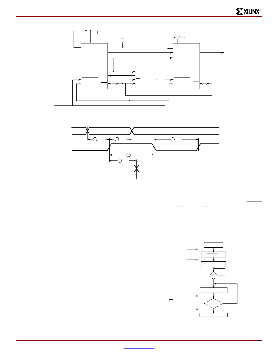
Architectural Description
Virtex-E Array
The Virtex-E user-programmable gate array, shown in
Figure 1
, comprises two major configurable elements: con-
figurable logic blocks (CLBs) and input/output blocks (IOBs).
∑
CLBs provide the functional elements for constructing
logic
∑
IOBs provide the interface between the package pins
and the CLBs
CLBs interconnect through a general routing matrix (GRM).
The GRM comprises an array of routing switches located at
the intersections of horizontal and vertical routing channels.
Each CLB nests into a VersaBlockTM that also provides local
routing resources to connect the CLB to the GRM.
The VersaRingTM I/O interface provides additional routing
resources around the periphery of the device. This routing
improves I/O routability and facilitates pin locking.
The Virtex-E architecture also includes the following circuits
that connect to the GRM.
∑
Dedicated block memories of 4096 bits each
∑
Clock DLLs for clock-distribution delay compensation
and clock domain control
∑
3-State buffers (BUFTs) associated with each CLB that
drive dedicated segmentable horizontal routing
resources
Values stored in static memory cells control the configurable
logic elements and interconnect resources. These values
load into the memory cells on power-up, and can reload if
necessary to change the function of the device.
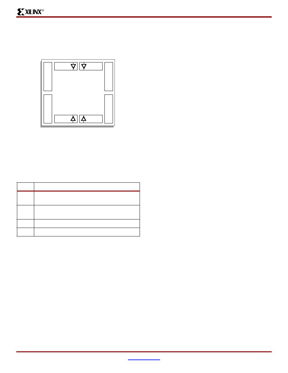
Input/Output Block
The Virtex-E IOB,
Figure 2
, features SelectI/O+ inputs and
outputs that support a wide variety of I/O signalling stan-
dards, see
Table 1
.
The three IOB storage elements function either as
edge-triggered D-type flip-flops or as level-sensitive latches.
Each IOB has a clock signal (CLK) shared by the three
flip-flops and independent clock enable signals for each
flip-flop.
0
VirtexTM-E 1.8 V
Field Programmable Gate Arrays
DS022-2 (v2.6) November 19, 2002
0
0
Production Product Specification
R
Figure 1: Virtex-E Architecture Overview
DLLDLL
IOBs
IOBs
VersaRing
VersaRing
ds022_01_121099
CLBs
BRAMs
BRAMs
BRAMs
CLBs
CLBs
BRAMs
CLBs
DLLDLL
DLLDLL
DLLDLL
Figure 2: Virtex-E Input/Output Block (IOB)
OBUFT
IBUF
Vref
ds022_02_091300
SR
CLK
ICE
OCE
O
I
IQ
T
TCE
D
CE
Q
SR
D
CE
Q
SR
D
CE
Q
SR
PAD
Programmable
Delay
Weak
Keeper
VirtexTM-E 1.8 V Field Programmable Gate Arrays
R
Module 2 of 4
www.xilinx.com
DS022-2 (v2.6) November 19, 2002
2
1-800-255-7778
Production Product Specification
In addition to the CLK and CE control signals, the three
flip-flops share a Set/Reset (SR). For each flip-flop, this sig-
nal can be independently configured as a synchronous Set,
a synchronous Reset, an asynchronous Preset, or an asyn-
chronous Clear.
The output buffer and all of the IOB control signals have
independent polarity controls.
All pads are protected against damage from electrostatic
discharge (ESD) and from over-voltage transients. After
configuration, clamping diodes are connected to V
CCO
with
the exception of LVCMOS18, LVCMOS25, GTL, GTL+,
LVDS, and LVPECL.
Optional pull-up, pull-down and weak-keeper circuits are
attached to each pad. Prior to configuration all outputs not
involved in configuration are forced into their high-imped-
ance state. The pull-down resistors and the weak-keeper
circuits are inactive, but I/Os can optionally be pulled up.
The activation of pull-up resistors prior to configuration is
controlled on a global basis by the configuration mode pins.
If the pull-up resistors are not activated, all the pins are in a
high-impedance state. Consequently, external pull-up or
pull-down resistors must be provided on pins required to be
at a well-defined logic level prior to configuration.
All Virtex-E IOBs support IEEE 1149.1-compatible bound-
ary scan testing.
Input Path
The Virtex-E IOB input path routes the input signal directly
to internal logic and/ or through an optional input flip-flop.
An optional delay element at the D-input of this flip-flop elim-
inates pad-to-pad hold time. The delay is matched to the
internal clock-distribution delay of the FPGA, and when
used, assures that the pad-to-pad hold time is zero.
Each input buffer can be configured to conform to any of the
low-voltage signalling standards supported. In some of
these standards the input buffer utilizes a user-supplied
threshold voltage, V
REF
. The need to supply V
REF
imposes
constraints on which standards can be used in close prox-
imity to each other. See
I/O Banking
.
There are optional pull-up and pull-down resistors at each
user I/O input for use after configuration. Their value is in
the range 50 ≠ 100 k
.
Output Path
The output path includes a 3-state output buffer that drives
the output signal onto the pad. The output signal can be
routed to the buffer directly from the internal logic or through
an optional IOB output flip-flop.
The 3-state control of the output can also be routed directly
from the internal logic or through a flip-flip that provides syn-
chronous enable and disable.
Each output driver can be individually programmed for a
wide range of low-voltage signalling standards. Each output
buffer can source up to 24 mA and sink up to 48 mA. Drive
strength and slew rate controls minimize bus transients.
In most signalling standards, the output High voltage
depends on an externally supplied V
CCO
voltage. The need
to supply V
CCO
imposes constraints on which standards
can be used in close proximity to each other. See
I/O Bank-
ing
.
An optional weak-keeper circuit is connected to each out-
put. When selected, the circuit monitors the voltage on the
pad and weakly drives the pin High or Low to match the
input signal. If the pin is connected to a multiple-source sig-
nal, the weak keeper holds the signal in its last state if all
drivers are disabled. Maintaining a valid logic level in this
way eliminates bus chatter.
Since the weak-keeper circuit uses the IOB input buffer to
monitor the input level, an appropriate V
REF
voltage must be
provided if the signalling standard requires one. The provi-
sion of this voltage must comply with the I/O banking rules.
I/O Banking
Some of the I/O standards described above require V
CCO
and/or V
REF
voltages. These voltages are externally sup-
plied and connected to device pins that serve groups of
IOBs, called banks. Consequently, restrictions exist about
which I/O standards can be combined within a given bank.
Table 1: Supported I/O Standards
I/O
Standard
Output
V
CCO
Input
V
CCO
Input
V
REF
Board
Termination
Voltage (V
TT
)
LVTTL
3.3
3.3
N/A
N/A
LVCMOS2
2.5
2.5
N/A
N/A
LVCMOS18
1.8
1.8
N/A
N/A
SSTL3 I & II
3.3
N/A
1.50
1.50
SSTL2 I & II
2.5
N/A
1.25
1.25
GTL
N/A
N/A
0.80
1.20
GTL+
N/A
N/A
1.0
1.50
HSTL I
1.5
N/A
0.75
0.75
HSTL III & IV
1.5
N/A
0.90
1.50
CTT
3.3
N/A
1.50
1.50
AGP-2X
3.3
N/A
1.32
N/A
PCI33_3 3.3
3.3
N/A
N/A
PCI66_3 3.3
3.3
N/A
N/A
BLVDS & LVDS
2.5
N/A
N/A
N/A
LVPECL
3.3
N/A
N/A
N/A
VirtexTM-E 1.8 V Field Programmable Gate Arrays
R
DS022-2 (v2.6) November 19, 2002
www.xilinx.com
Module 2 of 4
Production Product Specification
1-800-255-7778
3
Eight I/O banks result from separating each edge of the
FPGA into two banks, as shown in
Figure 3
. Each bank has
multiple V
CCO
pins, all of which must be connected to the
same voltage. This voltage is determined by the output
standards in use.
Within a bank, output standards can be mixed only if they
use the same V
CCO
. Compatible standards are shown in
Table 2
. GTL and GTL+ appear under all voltages because
their open-drain outputs do not depend on V
CCO
.
Some input standards require a user-supplied threshold
voltage, V
REF
. In this case, certain user-I/O pins are auto-
matically configured as inputs for the V
REF
voltage. Approx-
imately one in six of the I/O pins in the bank assume this
role.
The V
REF
pins within a bank are interconnected internally
and consequently only one V
REF
voltage can be used within
each bank. All V
REF
pins in the bank, however, must be con-
nected to the external voltage source for correct operation.
Within a bank, inputs that require V
REF
can be mixed with
those that do not. However, only one V
REF
voltage can be
used within a bank.
In Virtex-E, input buffers with LVTTL, LVCMOS2,
LVCMOS18, PCI33_3, PCI66_3 standards are supplied by
V
CCO
rather than V
CCINT
. For these standards, only input
and output buffers that have the same V
CCO
can be mixed
together.
The V
CCO
and V
REF
pins for each bank appear in the device
pin-out tables and diagrams. The diagrams also show the
bank affiliation of each I/O.
Within a given package, the number of V
REF
and V
CCO
pins
can vary depending on the size of device. In larger devices,
more I/O pins convert to V
REF
pins. Since these are always
a super set of the V
REF
pins used for smaller devices, it is
possible to design a PCB that permits migration to a larger
device if necessary. All the V
REF
pins for the largest device
anticipated must be connected to the V
REF
voltage, and not
used for I/O.
In smaller devices, some V
CCO
pins used in larger devices
do not connect within the package. These unconnected pins
can be left unconnected externally, or can be connected to
the V
CCO
voltage to permit migration to a larger device if
necessary.
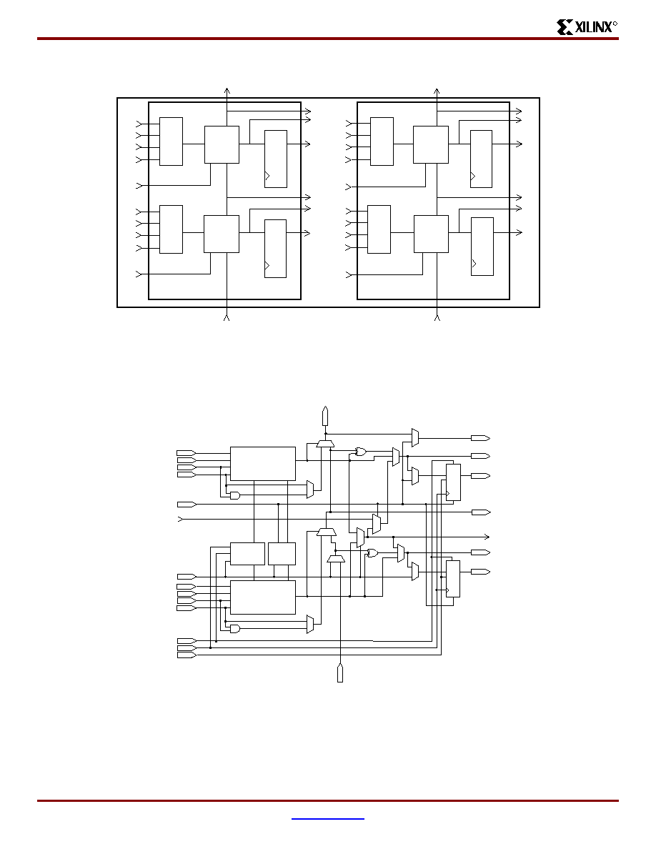
Configurable Logic Blocks
The basic building block of the Virtex-E CLB is the logic cell
(LC). An LC includes a 4-input function generator, carry
logic, and a storage element. The output from the function
generator in each LC drives both the CLB output and the D
input of the flip-flop. Each Virtex-E CLB contains four LCs,
organized in two similar slices, as shown in
Figure 4
.
Figure 5
shows a more detailed view of a single slice.
In addition to the four basic LCs, the Virtex-E CLB contains
logic that combines function generators to provide functions
of five or six inputs. Consequently, when estimating the
number of system gates provided by a given device, each
CLB counts as 4.5 LCs.
Look-Up Tables
Virtex-E function generators are implemented as 4-input
look-up tables (LUTs). In addition to operating as a function
generator, each LUT can provide a 16 x 1-bit synchronous
RAM. Furthermore, the two LUTs within a slice can be com-
bined to create a 16 x 2-bit or 32 x 1-bit synchronous RAM,
or a 16 x 1-bit dual-port synchronous RAM.
The Virtex-E LUT can also provide a 16-bit shift register that
is ideal for capturing high-speed or burst-mode data. This
mode can also be used to store data in applications such as
Digital Signal Processing.
Figure 3: Virtex-E I/O Banks
Table 2: Compatible Output Standards
V
CCO
Compatible Standards
3.3 V
PCI, LVTTL, SSTL3 I, SSTL3 II, CTT, AGP, GTL,
GTL+, LVPECL
2.5 V
SSTL2 I, SSTL2 II, LVCMOS2, GTL, GTL+,
BLVDS, LVDS
1.8 V
LVCMOS18, GTL, GTL+
1.5 V
HSTL I, HSTL III, HSTL IV, GTL, GTL+
ds022_03_121799
Bank 0
GCLK3 GCLK2
GCLK1 GCLK0
Bank 1
Bank 5
Bank 4
VirtexE
Device
Bank 7
Bank 6
Bank 2
Bank 3
VirtexTM-E 1.8 V Field Programmable Gate Arrays
R
Module 2 of 4
www.xilinx.com
DS022-2 (v2.6) November 19, 2002
4
1-800-255-7778
Production Product Specification
Storage Elements
The storage elements in the Virtex-E slice can be config-
ured either as edge-triggered D-type flip-flops or as
level-sensitive latches. The D inputs can be driven either by
the function generators within the slice or directly from slice
inputs, bypassing the function generators.
In addition to Clock and Clock Enable signals, each Slice
has synchronous set and reset signals (SR and BY). SR
Figure 4: 2-Slice Virtex-E CLB
F1
F2
F3
F4
G1
G2
G3
G4
Carry &
Control
Carry &
Control
Carry &
Control
Carry &
Control
LUT
CIN
CIN
COUT
COUT
YQ
XQ
XQ
YQ
X
XB
Y
YB
YB
Y
BX
BY
BX
BY
G1
G2
G3
G4
F1
F2
F3
F4
Slice 1
Slice 0
XB
X
LUT
LUT
LUT
D
CE
Q
RC
SP
D
CE
Q
RC
SP
D
CE
Q
RC
SP
D
CE
Q
RC
SP
ds022_04_121799
Figure 5: Detailed View of Virtex-E Slice
BY
F5IN
SR
CLK
CE
BX
YB
Y
YQ
XB
X
XQ
G4
G3
G2
G1
F4
F3
F2
F1
CIN
0
1
1
0
F5
F5
ds022_05_092000
COUT
CY
D
CE
Q
D
CE
Q
F6
CK
WSO
WSH
WE
A4
BY DG
BX
DI
DI
O
WE
I3
I2
I1
I0
LUT
CY
I3
I2
I1
I0
O
DI
WE
LUT
INIT
INIT
REV
REV

VirtexTM-E 1.8 V Field Programmable Gate Arrays
R
DS022-2 (v2.6) November 19, 2002
www.xilinx.com
Module 2 of 4
Production Product Specification
1-800-255-7778
5
forces a storage element into the initialization state speci-
fied for it in the configuration. BY forces it into the opposite
state. Alternatively, these signals can be configured to oper-
ate asynchronously. All of the control signals are indepen-
dently invertible, and are shared by the two flip-flops within
the slice.
Additional Logic
The F5 multiplexer in each slice combines the function gen-
erator outputs. This combination provides either a function
generator that can implement any 5-input function, a 4:1
multiplexer, or selected functions of up to nine inputs.
Similarly, the F6 multiplexer combines the outputs of all four
function generators in the CLB by selecting one of the
F5-multiplexer outputs. This permits the implementation of
any 6-input function, an 8:1 multiplexer, or selected func-
tions of up to 19 inputs.
Each CLB has four direct feedthrough paths, two per slice.
These paths provide extra data input lines or additional local
routing that does not consume logic resources.
Arithmetic Logic
Dedicated carry logic provides fast arithmetic carry capabil-
ity for high-speed arithmetic functions. The Virtex-E CLB
supports two separate carry chains, one per Slice. The
height of the carry chains is two bits per CLB.
The arithmetic logic includes an XOR gate that allows a
2-bit full adder to be implemented within a slice. In addition,
a dedicated AND gate improves the efficiency of multiplier
implementation. The dedicated carry path can also be used
to cascade function generators for implementing wide logic
functions.
BUFTs
Each Virtex-E CLB contains two 3-state drivers (BUFTs)
that can drive on-chip busses. See
Dedicated Routing
.
Each Virtex-E BUFT has an independent 3-state control pin
and an independent input pin.
Block SelectRAM
Virtex-E FPGAs incorporate large block SelectRAM memo-
ries. These complement the Distributed SelectRAM memo-
ries that provide shallow RAM structures implemented in
CLBs.
Block SelectRAM memory blocks are organized in columns,
starting at the left (column 0) and right outside edges and
inserted every 12 CLB columns (see notes for smaller
devices). Each memory block is four CLBs high, and each
memory column extends the full height of the chip, immedi-
ately adjacent (to the right, except for column 0) of the CLB
column locations indicated in
Table 3
.
Table 4
shows the amount of block SelectRAM memory that
is available in each Virtex-E device.
As illustrated in
Figure 6
, each block SelectRAM cell is a
fully synchronous dual-ported (True Dual Port) 4096-bit
RAM with independent control signals for each port. The
data widths of the two ports can be configured indepen-
dently, providing built-in bus-width conversion.
Table 3: CLB/Block RAM Column Locations
XCV
Device
/Col.
0 12 24
36 48
60
72
84
96
108
120
138
156
50E
Columns 0, 6, 18, & 24
100E
Columns 0, 12, 18, & 30
200E
Columns 0, 12, 30, & 42
300E
400E
600E
1000E
1600E
2000E
2600E
3200E
Table 4: Virtex-E Block SelectRAM Amounts
Virtex-E Device
# of Blocks
Block SelectRAM Bits
XCV50E
16
65,536
XCV100E
20
81,920
XCV200E
28
114,688
XCV300E
32
131,072
XCV400E
40
163,840
XCV600E
72
294,912
XCV1000E
96
393,216
XCV1600E
144
589,824
XCV2000E
160
655,360
XCV2600E
184
753,664
XCV3200E
208
851,968

VirtexTM-E 1.8 V Field Programmable Gate Arrays
R
Module 2 of 4
www.xilinx.com
DS022-2 (v2.6) November 19, 2002
6
1-800-255-7778
Production Product Specification
Table 5
shows the depth and width aspect ratios for the
block SelectRAM. The Virtex-E block SelectRAM also
includes dedicated routing to provide an efficient interface
with both CLBs and other block SelectRAMs. Refer to
XAPP130 for block SelectRAM timing waveforms.
Programmable Routing Matrix
It is the longest delay path that limits the speed of any
worst-case design. Consequently, the Virtex-E routing
architecture and its place-and-route software were defined
in a joint optimization process. This joint optimization mini-
mizes long-path delays, and consequently, yields the best
system performance.
The joint optimization also reduces design compilation
times because the architecture is software-friendly. Design
cycles are correspondingly reduced due to shorter design
iteration times.
Local Routing
The VersaBlock provides local routing resources (see
Figure 7
), providing three types of connections:
∑
Interconnections among the LUTs, flip-flops, and GRM
∑
Internal CLB feedback paths that provide high-speed
connections to LUTs within the same CLB, chaining
them together with minimal routing delay
∑
Direct paths that provide high-speed connections
between horizontally adjacent CLBs, eliminating the
delay of the GRM.
General Purpose Routing
Most Virtex-E signals are routed on the general purpose
routing, and consequently, the majority of interconnect
resources are associated with this level of the routing hier-
archy. General-purpose routing resources are located in
horizontal and vertical routing channels associated with the
CLB rows and columns and are as follows:
∑
Adjacent to each CLB is a General Routing Matrix
(GRM). The GRM is the switch matrix through which
horizontal and vertical routing resources connect, and
is also the means by which the CLB gains access to
the general purpose routing.
∑
24 single-length lines route GRM signals to adjacent
GRMs in each of the four directions.
∑
72 buffered Hex lines route GRM signals to another
GRMs six-blocks away in each one of the four
directions. Organized in a staggered pattern, Hex lines
are driven only at their endpoints. Hex-line signals can
be accessed either at the endpoints or at the midpoint
(three blocks from the source). One third of the Hex
lines are bidirectional, while the remaining ones are
uni-directional.
∑
12 Longlines are buffered, bidirectional wires that
distribute signals across the device quickly and
efficiently. Vertical Longlines span the full height of the
device, and horizontal ones span the full width of the
device.
I/O Routing
Virtex-E devices have additional routing resources around
their periphery that form an interface between the CLB array
and the IOBs. This additional routing, called the
VersaRing, facilitates pin-swapping and pin-locking, such
that logic redesigns can adapt to existing PCB layouts.
Time-to-market is reduced, since PCBs and other system
components can be manufactured while the logic design is
still in progress.
Figure 6: Dual-Port Block SelectRAM
Table 5: Block SelectRAM Port Aspect Ratios
Width
Depth
ADDR Bus
Data Bus
1
4096
ADDR<11:0>
DATA<0>
2
2048
ADDR<10:0>
DATA<1:0>
4
1024
ADDR<9:0>
DATA<3:0>
8
512
ADDR<8:0>
DATA<7:0>
16
256
ADDR<7:0>
DATA<15:0>
WEB
ENB
RSTB
CLKB
ADDRB[#:0]
DIB[#:0]
WEA
ENA
RSTA
CLKA
ADDRA[#:0]
DIA[#:0]
DOA[#:0]
DOB[#:0]
RAMB4_S#_S#
ds022_06_121699
Figure 7: Virtex-E Local Routing
XCVE_ds_007
CLB
GRM
To
Adjacent
GRM
To Adjacent
GRM
Direct
Connection
To Adjacent
CLB
To Adjacent
GRM
To Adjacent
GRM
Direct Connection
To Adjacent
CLB

VirtexTM-E 1.8 V Field Programmable Gate Arrays
R
DS022-2 (v2.6) November 19, 2002
www.xilinx.com
Module 2 of 4
Production Product Specification
1-800-255-7778
7
Dedicated Routing
Some classes of signal require dedicated routing resources to
maximize performance. In the Virtex-E architecture, dedi-
cated routing resources are provided for two classes of signal.
∑
Horizontal routing resources are provided for on-chip
3-state busses. Four partitionable bus lines are
provided per CLB row, permitting multiple busses
within a row, as shown in
Figure 8
.
∑
Two dedicated nets per CLB propagate carry signals
vertically to the adjacent CLB.Global Clock Distribution
Network
∑
DLL Location
Clock Routing
Clock Routing resources distribute clocks and other signals
with very high fanout throughout the device. Virtex-E
devices include two tiers of clock routing resources referred
to as global and local clock routing resources.
∑
The global routing resources are four dedicated global
nets with dedicated input pins that are designed to
distribute high-fanout clock signals with minimal skew.
Each global clock net can drive all CLB, IOB, and block
RAM clock pins. The global nets can be driven only by
global buffers. There are four global buffers, one for
each global net.
∑
The local clock routing resources consist of 24
backbone lines, 12 across the top of the chip and 12
across bottom. From these lines, up to 12 unique
signals per column can be distributed via the 12
longlines in the column. These local resources are
more flexible than the global resources since they are
not restricted to routing only to clock pins.
Global Clock Distribution
Virtex-E provides high-speed, low-skew clock distribution
through the global routing resources described above. A
typical clock distribution net is shown in
Figure 9
.
Four global buffers are provided, two at the top center of the
device and two at the bottom center. These drive the four
global nets that in turn drive any clock pin.
Four dedicated clock pads are provided, one adjacent to
each of the global buffers. The input to the global buffer is
selected either from these pads or from signals in the gen-
eral purpose routing.
Digital Delay-Locked Loops
There are eight DLLs (Delay-Locked Loops) per device,
with four located at the top and four at the bottom,
Figure 10
. The DLLs can be used to eliminate skew
between the clock input pad and the internal clock input pins
throughout the device. Each DLL can drive two global clock
networks.The DLL monitors the input clock and the distrib-
uted clock, and automatically adjusts a clock delay element.
Additional delay is introduced such that clock edges arrive
at internal flip-flops synchronized with clock edges arriving
at the input.
In addition to eliminating clock-distribution delay, the DLL
provides advanced control of multiple clock domains. The
DLL provides four quadrature phases of the source clock,
and can double the clock or divide the clock by 1.5, 2, 2.5, 3,
4, 5, 8, or 16.
Figure 8: BUFT Connections to Dedicated Horizontal Bus LInes
CLB
CLB
CLB
CLB
buft_c.eps
Tri-State
Lines
Figure 9: Global Clock Distribution Network
Gl
ob
al
Clo
c
k Sp
in
e
Global Clock Column
GCLKPAD2
GCLKBUF2
GCLKPAD3
GCLKBUF3
GCLKBUF1
GCLKPAD1
GCLKBUF0
GCLKPAD0
Global Clock Rows
XCVE_009
VirtexTM-E 1.8 V Field Programmable Gate Arrays
R
Module 2 of 4
www.xilinx.com
DS022-2 (v2.6) November 19, 2002
8
1-800-255-7778
Production Product Specification
The DLL also operates as a clock mirror. By driving the out-
put from a DLL off-chip and then back on again, the DLL can
be used to de-skew a board level clock among multiple
devices.
To guarantee that the system clock is operating correctly
prior to the FPGA starting up after configuration, the DLL
can delay the completion of the configuration process until
after it has achieved lock. For more information about DLL
functionality, see the Design Consideration section of the
data sheet.
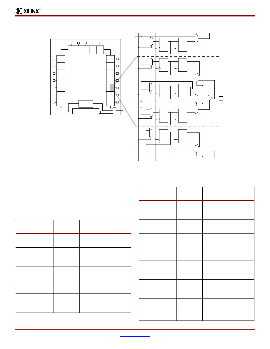
Boundary Scan
Virtex-E devices support all the mandatory boundary-scan
instructions specified in the IEEE standard 1149.1. A Test
Access Port (TAP) and registers are provided that imple-
ment the EXTEST, INTEST, SAMPLE/PRELOAD, BYPASS,
IDCODE, USERCODE, and HIGHZ instructions. The TAP
also supports two internal scan chains and configura-
tion/readback of the device.
The JTAG input pins (TDI, TMS, TCK) do not have a V
CCO
requirement and operate with either 2.5 V or 3.3 V input sig-
nalling levels. The output pin (TDO) is sourced from the
V
CCO
in bank 2, and for proper operation of LVTTL 3.3 V lev-
els, the bank should be supplied with 3.3 V.
Boundary-scan operation is independent of individual IOB
configurations, and unaffected by package type. All IOBs,
including un-bonded ones, are treated as independent
3-state bidirectional pins in a single scan chain. Retention of
the bidirectional test capability after configuration facilitates
the testing of external interconnections, provided the user
design or application is turned off.
Table 6
lists the boundary-scan instructions supported in
Virtex-E FPGAs. Internal signals can be captured during
EXTEST by connecting them to un-bonded or unused IOBs.
They can also be connected to the unused outputs of IOBs
defined as unidirectional input pins.
Before the device is configured, all instructions except
USER1 and USER2 are available. After configuration, all
instructions are available. During configuration, it is recom-
mended that those operations using the boundary-scan
register (SAMPLE/PRELOAD, INTEST, EXTEST) not be
performed.
In addition to the test instructions outlined above, the
boundary-scan circuitry can be used to configure the
FPGA, and also to read back the configuration data.
Figure 11
is a diagram of the Virtex-E Series boundary scan
logic. It includes three bits of Data Register per IOB, the
IEEE 1149.1 Test Access Port controller, and the Instruction
Register with decodes.
Figure 10: DLL Locations
XCVE_0010
DLLDLL
Primary DLLs
Secondar
y DLLs
Secondar
y DLLs
DLLDLL
DLLDLL
DLLDLL
VirtexTM-E 1.8 V Field Programmable Gate Arrays
R
DS022-2 (v2.6) November 19, 2002
www.xilinx.com
Module 2 of 4
Production Product Specification
1-800-255-7778
9
Instruction Set
The Virtex-E series boundary-scan instruction set also
includes instructions to configure the device and read back
configuration data (CFG_IN, CFG_OUT, and JSTART). The
complete instruction set is coded as shown in
Table 6
..
Figure 11: Virtex-E Family Boundary Scan Logic
D
Q
D
Q
IOB
IOB
IOB
IOB
IOB
IOB
IOB
IOB
IOB
IOB
IOB
IOB
IOB
M
U
X
BYPASS
REGISTER
IOB
IOB
TDO
TDI
IOB
IOB
IOB
1
0
1
0
1
0
1
0
1
0
sd
LE
D
Q
D
Q
D
Q
1
0
1
0
1
0
1
0
D
Q
LE
sd
sd
LE
D
Q
sd
LE
D
Q
IOB
D
Q
1
0
D
Q
LE
sd
IOB.T
DATA IN
IOB.I
IOB.Q
IOB.T
IOB.I
SHIFT/
CAPTURE
CLOCK DATA
REGISTER
DATAOUT
UPDATE
EXTEST
X9016
INSTRUCTION REGISTER
Table 6: Boundary Scan Instructions
Boundary-Scan
Command
Binary
Code(4:0)
Description
EXTEST
00000
Enables boundary-scan
EXTEST operation
SAMPLE/
PRELOAD
00001
Enables boundary-scan
SAMPLE/PRELOAD
operation
USER1
00010
Access user-defined
register 1
USER2
00011
Access user-defined
register 2
CFG_OUT
00100
Access the
configuration bus for
read operations.
CFG_IN
00101
Access the
configuration bus for
write operations.
INTEST
00111
Enables boundary-scan
INTEST operation
USERCODE
01000
Enables shifting out
USER code
IDCODE
01001
Enables shifting out of
ID Code
HIGHZ
01010
3-states output pins
while enabling the
Bypass Register
JSTART
01100
Clock the start-up
sequence when
StartupClk is TCK
BYPASS
11111
Enables BYPASS
RESERVED
All other
codes
Xilinx reserved
instructions
Table 6: Boundary Scan Instructions (Continued)
Boundary-Scan
Command
Binary
Code(4:0)
Description

VirtexTM-E 1.8 V Field Programmable Gate Arrays
R
Module 2 of 4
www.xilinx.com
DS022-2 (v2.6) November 19, 2002
10
1-800-255-7778
Production Product Specification
Data Registers
The primary data register is the boundary scan register. For
each IOB pin in the FPGA, bonded or not, it includes three
bits for In, Out, and 3-State Control. Non-IOB pins have
appropriate partial bit population if input-only or output-only.
Each EXTEST CAPTURED-OR state captures all In, Out,
and 3-state pins.
The other standard data register is the single flip-flop
BYPASS register. It synchronizes data being passed
through the FPGA to the next downstream boundary scan
device.
The FPGA supports up to two additional internal scan
chains that can be specified using the BSCAN macro. The
macro provides two user pins (SEL1 and SEL2) which are
decodes of the USER1 and USER2 instructions respec-
tively. For these instructions, two corresponding pins (T
DO1 and TDO2) allow user scan data to be shifted out of
TDO.
Likewise, there are individual clock pins (DRCK1 and
DRCK2) for each user register. There is a common input pin
(TDI) and shared output pins that represent the state of the
TAP controller (RESET, SHIFT, and UPDATE).
Bit Sequence
The order within each IOB is: In, Out, 3-State. The
input-only pins contribute only the In bit to the boundary
scan I/O data register, while the output-only pins contributes
all three bits.
From a cavity-up view of the chip (as shown in EPIC), start-
ing in the upper right chip corner, the boundary scan
data-register bits are ordered as shown in
Figure 12
.
BSDL (Boundary Scan Description Language) files for Vir-
tex-E Series devices are available on the Xilinx web site in
the File Download area.
Identification Registers
The IDCODE register is supported. By using the IDCODE,
the device connected to the JTAG port can be determined.
The IDCODE register has the following binary format:
vvvv:ffff:fffa:aaaa:aaaa:cccc:cccc:ccc1
where
v = the die version number
f = the family code (05 for Virtex-E family)
a = the number of CLB rows (ranges from 16 for
XCV50E to 104 for XCV3200E)
c = the company code (49h for Xilinx)
The USERCODE register is supported. By using the USER-
CODE, a user-programmable identification code can be
loaded and shifted out for examination. The identification
code (see
Table 7
) is embedded in the bitstream during bit-
stream generation and is valid only after configuration.
Note:
Attempting to load an incorrect bitstream causes
configuration to fail and can damage the device.
Including Boundary Scan in a Design
Since the boundary scan pins are dedicated, no special ele-
ment needs to be added to the design unless an internal
data register (USER1 or USER2) is desired.
If an internal data register is used, insert the boundary scan
symbol and connect the necessary pins as appropriate.
Figure 12: Boundary Scan Bit Sequence
Bit 0 ( TDO end)
Bit 1
Bit 2
Right half of top-edge IOBs (Right to Left)
GCLK2
GCLK3
Left half of top-edge IOBs (Right to Left)
Left-edge IOBs (Top to Bottom)
M1
M0
M2
Left half of bottom-edge IOBs (Left to Right)
GCLK1
GCLK0
Right half of bottom-edge IOBs (Left to Right)
DONE
PROG
Right-edge IOBs (Bottom to Top)
CCLK
(TDI end)
990602001
Table 7: IDCODEs Assigned to Virtex-E FPGAs
FPGA
IDCODE
XCV50E
v0A10093h
XCV100E
v0A14093h
XCV200E
v0A1C093h
XCV300E
v0A20093h
XCV400E
v0A28093h
XCV600E
v0A30093h
XCV1000E
v0A40093h
XCV1600E
v0A48093h
XCV2000E
v0A50093h
XCV2600E
v0A5C093h
XCV3200E
v0A68093h

VirtexTM-E 1.8 V Field Programmable Gate Arrays
R
DS022-2 (v2.6) November 19, 2002
www.xilinx.com
Module 2 of 4
Production Product Specification
1-800-255-7778
11
Development System
Virtex-E FPGAs are supported by the Xilinx Foundation and
Alliance Series CAE tools. The basic methodology for
Virtex-E design consists of three interrelated steps: design
entry, implementation, and verification. Industry-standard
tools are used for design entry and simulation (for example,
Synopsys FPGA Express), while Xilinx provides proprietary
architecture-specific tools for implementation.
The Xilinx development system is integrated under the
Xilinx Design Manager (XDMTM) software, providing design-
ers with a common user interface regardless of their choice
of entry and verification tools. The XDM software simplifies
the selection of implementation options with pull-down
menus and on-line help.
Application programs ranging from schematic capture to
Placement and Routing (PAR) can be accessed through the
XDM software. The program command sequence is gener-
ated prior to execution, and stored for documentation.
Several advanced software features facilitate Virtex-E design.
RPMs, for example, are schematic-based macros with relative
location constraints to guide their placement. They help
ensure optimal implementation of common functions.
For HDL design entry, the Xilinx FPGA Foundation develop-
ment system provides interfaces to the following synthesis
design environments.
∑
Synopsys (FPGA Compiler, FPGA Express)
∑
Exemplar (Spectrum)
∑
Synplicity (Synplify)
For schematic design entry, the Xilinx FPGA Foundation
and Alliance development system provides interfaces to the
following schematic-capture design environments.
∑
Mentor Graphics V8 (Design Architect, QuickSim II)
∑
Viewlogic Systems (Viewdraw)
Third-party vendors support many other environments.
A standard interface-file specification, Electronic Design
Interchange Format (EDIF), simplifies file transfers into and
out of the development system.
Virtex-E FPGAs are supported by a unified library of stan-
dard functions. This library contains over 400 primitives and
macros, ranging from 2-input AND gates to 16-bit accumu-
lators, and includes arithmetic functions, comparators,
counters, data registers, decoders, encoders, I/O functions,
latches, Boolean functions, multiplexers, shift registers, and
barrel shifters.
The "soft macro" portion of the library contains detailed
descriptions of common logic functions, but does not con-
tain any partitioning or placement information. The perfor-
mance of these macros depends, therefore, on the
partitioning and placement obtained during implementation.
RPMs, on the other hand, do contain predetermined parti-
tioning and placement information that permits optimal
implementation of these functions. Users can create their
own library of soft macros or RPMs based on the macros
and primitives in the standard library.
The design environment supports hierarchical design entry,
with high-level schematics that comprise major functional
blocks, while lower-level schematics define the logic in
these blocks. These hierarchical design elements are auto-
matically combined by the implementation tools. Different
design entry tools can be combined within a hierarchical
design, thus allowing the most convenient entry method to
be used for each portion of the design.
Design Implementation
The place-and-route tools (PAR) automatically provide the
implementation flow described in this section. The parti-
tioner takes the EDIF net list for the design and maps the
logic into the architectural resources of the FPGA (CLBs
and IOBs, for example). The placer then determines the
best locations for these blocks based on their interconnec-
tions and the desired performance. Finally, the router inter-
connects the blocks.
The PAR algorithms support fully automatic implementation
of most designs. For demanding applications, however, the
user can exercise various degrees of control over the pro-
cess. User partitioning, placement, and routing information
is optionally specified during the design-entry process. The
implementation of highly structured designs can benefit
greatly from basic floor planning.
The implementation software incorporates Timing Wizard
Æ
timing-driven placement and routing. Designers specify tim-
ing requirements along entire paths during design entry.
The timing path analysis routines in PAR then recognize
these user-specified requirements and accommodate them.
Timing requirements are entered on a schematic in a form
directly relating to the system requirements, such as the tar-
geted clock frequency, or the maximum allowable delay
between two registers. In this way, the overall performance
of the system along entire signal paths is automatically tai-
lored to user-generated specifications. Specific timing infor-
mation for individual nets is unnecessary.
Design Verification
In addition to conventional software simulation, FPGA users
can use in-circuit debugging techniques. Because Xilinx
devices are infinitely reprogrammable, designs can be veri-
fied in real time without the need for extensive sets of soft-
ware simulation vectors.
The development system supports both software simulation
and in-circuit debugging techniques. For simulation, the
system extracts the post-layout timing information from the
design database, and back-annotates this information into
the net list for use by the simulator. Alternatively, the user
can verify timing-critical portions of the design using the
TRCE
Æ
static timing analyzer.
VirtexTM-E 1.8 V Field Programmable Gate Arrays
R
Module 2 of 4
www.xilinx.com
DS022-2 (v2.6) November 19, 2002
12
1-800-255-7778
Production Product Specification
For in-circuit debugging, an optional download and read-
back cable is available. This cable connects the FPGA in the
target system to a PC or workstation. After downloading the
design into the FPGA, the designer can single-step the
logic, readback the contents of the flip-flops, and so observe
the internal logic state. Simple modifications can be down-
loaded into the system in a matter of minutes.
Configuration
Virtex-E devices are configured by loading configuration
data into the internal configuration memory. Note that
attempting to load an incorrect bitstream causes configura-
tion to fail and can damage the device.
Some of the pins used for configuration are dedicated pins,
while others can be re-used as general purpose inputs and
outputs once configuration is complete.
The following are dedicated pins:
∑
Mode pins (M2, M1, M0)
∑
Configuration clock pin (CCLK)
∑
PROGRAM pin
∑
DONE pin
∑
Boundary-scan pins (TDI, TDO, TMS, TCK)
Depending on the configuration mode chosen, CCLK can
be an output generated by the FPGA, or can be generated
externally and provided to the FPGA as an input. The
PROGRAM pin must be pulled High prior to reconfiguration.
Note that some configuration pins can act as outputs. For
correct operation, these pins require a V
CCO
of 3.3 V or
2.5 V. At 3.3 V the pins operate as LVTTL, and at 2.5 V they
operate as LVCMOS. All affected pins fall in banks 2 or 3.
The configuration pins needed for SelectMap (CS, Write)
are located in bank 1.
Configuration Modes
Virtex-E supports the following four configuration modes.
∑
Slave-serial mode
∑
Master-serial mode
∑
SelectMAP mode
∑
Boundary-scan mode (JTAG)
The Configuration mode pins (M2, M1, M0) select among
these configuration modes with the option in each case of
having the IOB pins either pulled up or left floating prior to
configuration. The selection codes are listed in
Table 8
.
Configuration through the boundary-scan port is always
available, independent of the mode selection. Selecting the
boundary-scan mode simply turns off the other modes. The
three mode pins have internal pull-up resistors, and default
to a logic High if left unconnected. However, it is recom-
mended to drive the configuration mode pins externally.
Table 8: Configuration Codes
Configuration Mode
M2
M1
M0
CCLK Direction
Data Width
Serial D
out
Configuration Pull-ups
Master-serial mode
0
0
0
Out
1
Yes
No
Boundary-scan mode
1
0
1
N/A
1
No
No
SelectMAP mode
1
1
0
In
8
No
No
Slave-serial mode
1
1
1
In
1
Yes
No
Master-serial mode
1
0
0
Out
1
Yes
Yes
Boundary-scan mode
0
0
1
N/A
1
No
Yes
SelectMAP mode
0
1
0
In
8
No
Yes
Slave-serial mode
0
1
1
In
1
Yes
Yes

VirtexTM-E 1.8 V Field Programmable Gate Arrays
R
DS022-2 (v2.6) November 19, 2002
www.xilinx.com
Module 2 of 4
Production Product Specification
1-800-255-7778
13
Table 9
lists the total number of bits required to configure
each device.
Slave-Serial Mode
In slave-serial mode, the FPGA receives configuration data
in bit-serial form from a serial PROM or other source of
serial configuration data. The serial bitstream must be set
up at the DIN input pin a short time before each rising edge
of an externally generated CCLK.
For more detailed information on serial PROMs, see the
PROM data sheet at
http://www.xilinx.com/bvdocs/publi-
cations/ds026.pdf
.
Multiple FPGAs can be daisy-chained for configuration from a
single source. After a particular FPGA has been configured,
the data for the next device is routed to the DOUT pin. The
data on the DOUT pin changes on the rising edge of CCLK.
The change of DOUT on the rising edge of CCLK differs
from previous families, but does not cause a problem for
mixed configuration chains. This change was made to
improve serial configuration rates for Virtex and Virtex-E
only chains.
Figure 13
shows a full master/slave system. A Virtex-E
device in slave-serial mode should be connected as shown
in the right-most device.
Slave-serial mode is selected by applying <111> or <011> to
the mode pins (M2, M1, M0). A weak pull-up on the mode pins
makes slave serial the default mode if the pins are left uncon-
nected. However, it is recommended to drive the configura-
tion mode pins externally.
Figure 14
shows slave-serial
mode programming switching characteristics.
Table 10
provides more detail about the characteristics
shown in
Figure 14
. Configuration must be delayed until the
INIT pins of all daisy-chained FPGAs are High.
Table 9: Virtex-E Bitstream Lengths
Device
# of Configuration Bits
XCV50E
630,048
XCV100E
863,840
XCV200E
1,442,016
XCV300E
1, 875,648
XCV400E
2,693,440
XCV600E
3,961,632
XCV1000E
6,587,520
XCV1600E
8,308,992
XCV2000E
10,159,648
XCV2600E
12,922,336
XCV3200E
16,283,712
Table 10: Master/Slave Serial Mode Programming Switching
Description
Figure
References
Symbol
Values
Units
CCLK
DIN setup/hold, slave mode
1/2
T
DCC
/T
CCD
5.0 / 0.0
ns, min
DIN setup/hold, master mode
1/2
T
DSCK
/T
CKDS
5.0 / 0.0
ns, min
DOUT
3
T
CCO
12.0
ns, max
High time
4
T
CCH
5.0
ns, min
Low time
5
T
CCL
5.0
ns, min
Maximum Frequency
F
CC
66
MHz, max
Frequency Tolerance, master mode with respect to nominal
+45% ≠30%
VirtexTM-E 1.8 V Field Programmable Gate Arrays
R
Module 2 of 4
www.xilinx.com
DS022-2 (v2.6) November 19, 2002
14
1-800-255-7778
Production Product Specification
.
Master-Serial Mode
In master-serial mode, the CCLK output of the FPGA drives
a Xilinx Serial PROM that feeds bit-serial data to the DIN
input. The FPGA accepts this data on each rising CCLK
edge. After the FPGA has been loaded, the data for the next
device in a daisy-chain is presented on the DOUT pin after
the rising CCLK edge.
The interface is identical to slave-serial except that an inter-
nal oscillator is used to generate the configuration clock
(CCLK). A wide range of frequencies can be selected for
CCLK, which always starts at a slow default frequency. Con-
figuration bits then switch CCLK to a higher frequency for
the remainder of the configuration. Switching to a lower fre-
quency is prohibited.
The CCLK frequency is set using the ConfigRate option in
the bitstream generation software. The maximum CCLK fre-
quency that can be selected is 60 MHz. When selecting a
CCLK frequency, ensure that the serial PROM and any
daisy-chained FPGAs are fast enough to support the clock
rate.
On power-up, the CCLK frequency is approximately
2.5 MHz. This frequency is used until the ConfigRate bits
have been loaded when the frequency changes to the
selected ConfigRate. Unless a different frequency is speci-
fied in the design, the default ConfigRate is 4 MHz.
In a full master/slave system (
Figure 13
), the left-most
device operates in master-serial mode. The remaining
devices operate in slave-serial mode. The SPROM RESET
pin is driven by INIT, and the CE input is driven by DONE.
There is the potential for contention on the DONE pin,
depending on the start-up sequence options chosen.
The sequence of operations necessary to configure a
Virtex-E FPGA serially appears in
Figure 15
.
Figure 13: Master/Slave Serial Mode Circuit Diagram
VIRTEX-E
MASTER
SERIAL
VIRTEX-E,
XC4000XL,
SLAVE
XC1701L
PROGRAM
M2
M0 M1
DOUT
CCLK
CLK
3.3V
DATA
CE
CEO
RESET/OE
DONE
DIN
INIT
INIT
DONE
PROGRAM
PROGRAM
CCLK
DIN
DOUT
M2
M0 M1
(Low Reset Option Used)
4.7 K
XCVE_ds_013
N/C
N/C
Figure 14: Slave-Serial Mode Programming Switching Characteristics
4 T
CCH
3 T
CCO
5 T
CCL
2 T
CCD
1 T
DCC
DIN
CCLK
DOUT
(Output)
X5379_a
Figure 15: Serial Configuration Flowchart
Apply Power
Set PROGRAM = High
Release INIT
If used to delay
configuration
Load a Configuration Bit
High
Low
FPGA makes a final
clearing pass and releases
INIT when finished.
FPGA starts to clear
configuration memory.
ds009_15_111799
Configuration Completed
End of
Bitstream?
Yes
No
Once per bitstream,
FPGA checks data using CRC
and pulls INIT Low on error.
If no CRC errors found,
FPGA enters start-up phase
causing DONE to go High.
INIT?

VirtexTM-E 1.8 V Field Programmable Gate Arrays
R
DS022-2 (v2.6) November 19, 2002
www.xilinx.com
Module 2 of 4
Production Product Specification
1-800-255-7778
15
Figure 16
shows the timing of master-serial configuration.
Master-serial mode is selected by a <000> or <100> on the
mode pins (M2, M1, M0).
Table 10
shows the timing infor-
mation for
Figure 16
.
At power-up, V
CC
must rise from 1.0 V to V
CC
Min in less
than 50 ms, otherwise delay configuration by pulling
PROGRAM Low until V
CC
is valid.
SelectMAP Mode
The SelectMAP mode is the fastest configuration option.
Byte-wide data is written into the FPGA with a BUSY flag
controlling the flow of data.
An external data source provides a byte stream, CCLK, a
Chip Select (CS) signal and a Write signal (WRITE). If
BUSY is asserted (High) by the FPGA, the data must be
held until BUSY goes Low.
Data can also be read using the SelectMAP mode. If
WRITE is not asserted, configuration data is read out of the
FPGA as part of a readback operation.
After configuration, the pins of the SelectMAP port can be
used as additional user I/O. Alternatively, the port can be
retained to permit high-speed 8-bit readback.
Retention of the SelectMAP port is selectable on a
design-by-design basis when the bitstream is generated. If
retention is selected, PROHIBIT constraints are required to
prevent the SelectMAP-port pins from being used as user
I/O.
Multiple Virtex-E FPGAs can be configured using the
SelectMAP mode, and be made to start-up simultaneously.
To configure multiple devices in this way, wire the individual
CCLK, Data, WRITE, and BUSY pins of all the devices in
parallel. The individual devices are loaded separately by
asserting the CS pin of each device in turn and writing the
appropriate data. See
Table 11
for SelectMAP Write Timing
Characteristics.
Write
Write operations send packets of configuration data into the
FPGA. The sequence of operations for a multi-cycle write
operation is shown below. Note that a configuration packet
can be split into many such sequences. The packet does
not have to complete within one assertion of CS, illustrated
in
Figure 17
.
1.
Assert WRITE and CS Low. Note that when CS is
asserted on successive CCLKs, WRITE must remain
either asserted or de-asserted. Otherwise, an abort is
initiated, as described below.
2.
Drive data onto D[7:0]. Note that to avoid contention,
the data source should not be enabled while CS is Low
and WRITE is High. Similarly, while WRITE is High, no
more that one CS should be asserted.
3.
At the rising edge of CCLK: If BUSY is Low, the data is
accepted on this clock. If BUSY is High (from a previous
write), the data is not accepted. Acceptance instead
occurs on the first clock after BUSY goes Low, and the
data must be held until this has happened.
4.
Repeat steps 2 and 3 until all the data has been sent.
5.
De-assert CS and WRITE.
Figure 16: Master-Serial Mode Programming Switching Characteristics
Serial Data In
CCLK
(Output)
Serial DOUT
(Output)
1 TDSCK
2
TCKDS
DS022_44_071201

VirtexTM-E 1.8 V Field Programmable Gate Arrays
R
Module 2 of 4
www.xilinx.com
DS022-2 (v2.6) November 19, 2002
16
1-800-255-7778
Production Product Specification
A flowchart for the write operation is shown in
Figure 18
.
Note that if CCLK is slower than f
CCNH
, the FPGA never
asserts BUSY, In this case, the above handshake is unnec-
essary, and data can simply be entered into the FPGA every
CCLK cycle.
Abort
During a given assertion of CS, the user cannot switch from
a write to a read, or vice-versa. This action causes the cur-
rent packet command to be aborted. The device remains
BUSY until the aborted operation has completed. Following
an abort, data is assumed to be unaligned to word bound-
aries, and the FPGA requires a new synchronization word
prior to accepting any new packets.
To initiate an abort during a write operation, de-assert
WRITE. At the rising edge of CCLK, an abort is initiated, as
shown in
Figure 19
.
Table 11: SelectMAP Write Timing Characteristics
Description
Symbol
Units
CCLK
D
0-7
Setup/Hold 1/2
T
SMDCC
/T
SMCCD
5.0 / 1.7
ns, min
CS Setup/Hold
3/4
T
SMCSCC
/T
SMCCCS
7.0 / 1.7
ns, min
WRITE Setup/Hold
5/6
T
SMCCW
/T
SMWCC
7.0 / 1.7
ns, min
BUSY Propagation Delay
7
T
SMCKBY
12.0
ns, max
Maximum Frequency
F
CC
66
MHz, max
Maximum Frequency with no handshake
F
CCNH
50
MHz, max
Figure 17: Write Operations
DS022_45_071702
CCLK
No Write
Write
No Write
Write
DATA[0:7]
CS
WRITE
3
5
BUSY
4
6
7
1
2

VirtexTM-E 1.8 V Field Programmable Gate Arrays
R
DS022-2 (v2.6) November 19, 2002
www.xilinx.com
Module 2 of 4
Production Product Specification
1-800-255-7778
17
Boundary-Scan Mode
In the boundary-scan mode, configuration is done through
the IEEE 1149.1 Test Access Port. Note that the
PROGRAM pin must be pulled High prior to reconfiguration.
A Low on the PROGRAM pin resets the TAP controller and
no JTAG operations can be performed.
Figure 18: SelectMAP Flowchart for Write Operations
Apply Power
Release INIT
If used to delay
configuration
On first FPGA
PROGRAM
from Low
to High
Set WRITE = Low
Enter Data Source
Set CS = Low
On first FPGA
Set CS = High
Apply Configuration Byte
INIT?
High
Low
Yes
No
Busy?
Low
High
Disable Data Source
Set WRITE = High
When all DONE pins
are released, DONE goes High
and start-up sequences complete.
If no errors,
later FPGAs enter start-up phase
releasing DONE.
If no errors,
first FPGAs enter start-up phase
releasing DONE.
Once per bitstream,
FPGA checks data using CRC
and pulls INIT Low on error.
FPGA makes a final
clearing pass and releases
INIT when finished.
FPGA starts to clear
configuration memory.
For any other FPGAs
ds003_17_090602
Repeat Sequence A
Configuration Completed
Sequence A
End of Data?
Yes
No
Figure 19: SelectMAP Write Abort Waveforms
CCLK
CS
WRITE
Abort
DATA[0:7]
BUSY
DS022_46_071702

VirtexTM-E 1.8 V Field Programmable Gate Arrays
R
Module 2 of 4
www.xilinx.com
DS022-2 (v2.6) November 19, 2002
18
1-800-255-7778
Production Product Specification
Configuration through the TAP uses the CFG_IN instruc-
tion. This instruction allows data input on TDI to be con-
verted into data packets for the internal configuration bus.
The following steps are required to configure the FPGA
through the boundary-scan port (when using TCK as a
start-up clock).
1.
Load the CFG_IN instruction into the boundary-scan
instruction register (IR).
2.
Enter the Shift-DR (SDR) state.
3.
Shift a configuration bitstream into TDI.
4.
Return to Run-Test-Idle (RTI).
5.
Load the JSTART instruction into IR.
6.
Enter the SDR state.
7.
Clock TCK through the startup sequence.
8.
Return to RTI.
Configuration and readback via the TAP is always available.
The boundary-scan mode is selected by a <101> or <001>
on the mode pins (M2, M1, M0). For details on TAP charac-
teristics, refer to XAPP139.
Configuration Sequence
The configuration of Virtex-E devices is a three-phase pro-
cess. First, the configuration memory is cleared. Next, con-
figuration data is loaded into the memory, and finally, the
logic is activated by a start-up process.
Configuration is automatically initiated on power-up unless
it is delayed by the user, as described below. The configura-
tion process can also be initiated by asserting PROGRAM.
The end of the memory-clearing phase is signalled by INIT
going High, and the completion of the entire process is sig-
nalled by DONE going High.
The power-up timing of configuration signals is shown in
Figure 20
.
The corresponding timing characteristics are listed in
Table 12
.
Delaying Configuration
INIT can be held Low using an open-drain driver. An
open-drain is required since INIT is a bidirectional
open-drain pin that is held Low by the FPGA while the con-
figuration memory is being cleared. Extending the time that
the pin is Low causes the configuration sequencer to wait.
Thus, configuration is delayed by preventing entry into the
phase where data is loaded.
Start-Up Sequence
The default Start-up sequence is that one CCLK cycle after
DONE goes High, the global 3-state signal (GTS) is
released. This permits device outputs to turn on as neces-
sary.
One CCLK cycle later, the Global Set/Reset (GSR) and Glo-
bal Write Enable (GWE) signals are released. This permits
Figure 20: Power-Up Timing Configuration Signals
VALI
PROGRAM
Vcc
CCLK OUTPUT or INPUT
M0, M1, M2
(Required)
TPL
TICCK
ds022_020_071201
TPOR
INIT
Table 12: Power-up Timing Characteristics
Description
Symbol
Value
Units
Power-on Reset
1
T
POR
2.0
ms, max
Program Latency
T
PL
100.0
µ
s, max
CCLK (output) Delay
T
ICCK
0.5
µ
s, min
4.0
µ
s, max
Program Pulse Width
T
PROGRAM
300
ns, min
Notes:
1.
T
POR
delay is the initialization time required after V
CCINT
and
V
CCO
in Bank 2 reach the recommended operating voltage.

VirtexTM-E 1.8 V Field Programmable Gate Arrays
R
DS022-2 (v2.6) November 19, 2002
www.xilinx.com
Module 2 of 4
Production Product Specification
1-800-255-7778
19
the internal storage elements to begin changing state in
response to the logic and the user clock.
The relative timing of these events can be changed. In addi-
tion, the GTS, GSR, and GWE events can be made depen-
dent on the DONE pins of multiple devices all going High,
forcing the devices to start synchronously. The sequence
can also be paused at any stage until lock has been
achieved on any or all DLLs.
Readback
The configuration data stored in the Virtex-E configuration
memory can be readback for verification. Along with the
configuration data it is possible to readback the contents all
flip-flops/latches, LUT RAMs, and block RAMs. This capa-
bility is used for real-time debugging. For more detailed
information, see application note XAPP138 "Virtex FPGA
Series Configuration and Readback".
Design Considerations
This section contains more detailed design information on
the following features.
∑
Delay-Locked Loop . . . see
page 19
∑
BlockRAM . . . see
page 24
∑
SelectI/O . . . see
page 31
Using DLLs
The Virtex-E FPGA series provides up to eight fully digital
dedicated on-chip Delay-Locked Loop (DLL) circuits which
provide zero propagation delay, low clock skew between
output clock signals distributed throughout the device, and
advanced clock domain control. These dedicated DLLs can
be used to implement several circuits which improve and
simplify system level design.
Introduction
As FPGAs grow in size, quality on-chip clock distribution
becomes increasingly important. Clock skew and clock
delay impact device performance and the task of managing
clock skew and clock delay with conventional clock trees
becomes more difficult in large devices. The Virtex-E series
of devices resolve this potential problem by providing up to
eight fully digital dedicated on-chip DLL circuits, which pro-
vide zero propagation delay and low clock skew between
output clock signals distributed throughout the device.
Each DLL can drive up to two global clock routing networks
within the device. The global clock distribution network min-
imizes clock skews due to loading differences. By monitor-
ing a sample of the DLL output clock, the DLL can
compensate for the delay on the routing network, effectively
eliminating the delay from the external input port to the indi-
vidual clock loads within the device.
In addition to providing zero delay with respect to a user
source clock, the DLL can provide multiple phases of the
source clock. The DLL can also act as a clock doubler or it
can divide the user source clock by up to 16.
Clock multiplication gives the designer a number of design
alternatives. For instance, a 50 MHz source clock doubled
by the DLL can drive an FPGA design operating at 100
MHz. This technique can simplify board design because the
clock path on the board no longer distributes such a
high-speed signal. A multiplied clock also provides design-
ers the option of time-domain-multiplexing, using one circuit
twice per clock cycle, consuming less area than two copies
of the same circuit. Two DLLs in can be connected in series
to increase the effective clock multiplication factor to four.
The DLL can also act as a clock mirror. By driving the DLL
output off-chip and then back in again, the DLL can be used
to de-skew a board level clock between multiple devices.
In order to guarantee the system clock establishes prior to
the device "waking up," the DLL can delay the completion of
the device configuration process until after the DLL
achieves lock.
By taking advantage of the DLL to remove on-chip clock
delay, the designer can greatly simplify and improve system
level design involving high-fanout, high-performance clocks.
Library DLL Symbols
Figure 21
shows the simplified Xilinx library DLL macro
symbol, BUFGDLL. This macro delivers a quick and effi-
cient way to provide a system clock with zero propagation
delay throughout the device.
Figure 22
and
Figure 23
show
the two library DLL primitives. These symbols provide
access to the complete set of DLL features when imple-
menting more complex applications.
Figure 21: Simplified DLL Macro Symbol BUFGDLL
0ns
ds022_25_121099
O
I
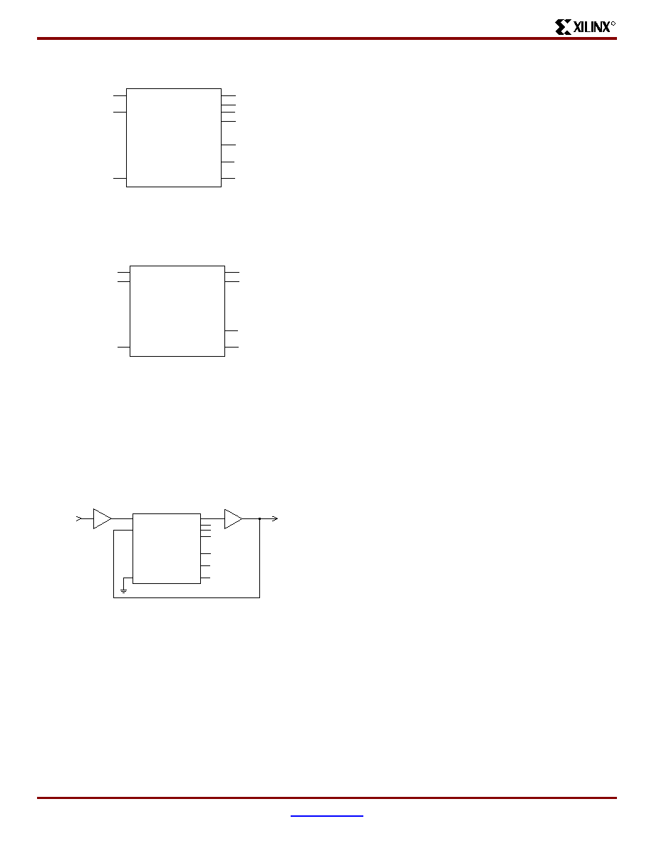
VirtexTM-E 1.8 V Field Programmable Gate Arrays
R
Module 2 of 4
www.xilinx.com
DS022-2 (v2.6) November 19, 2002
20
1-800-255-7778
Production Product Specification
BUFGDLL Pin Descriptions
Use the BUFGDLL macro as the simplest way to provide
zero propagation delay for a high-fanout on-chip clock from
an external input. This macro uses the IBUFG, CLKDLL and
BUFG primitives to implement the most basic DLL applica-
tion as shown in
Figure 24
.
This symbol does not provide access to the advanced clock
domain controls or to the clock multiplication or clock divi-
sion features of the DLL. This symbol also does not provide
access to the RST, or LOCKED pins of the DLL. For access
to these features, a designer must use the library DLL prim-
itives described in the following sections.
Source Clock Input -- I
The I pin provides the user source clock, the clock signal on
which the DLL operates, to the BUFGDLL. For the BUF-
GDLL macro the source clock frequency must fall in the low
frequency range as specified in the data sheet. The BUF-
GDLL requires an external signal source clock. Therefore,
only an external input port can source the signal that drives
the BUFGDLL I pin.
Clock Output -- O
The clock output pin O represents a delay-compensated
version of the source clock (I) signal. This signal, sourced by
a global clock buffer BUFG symbol, takes advantage of the
dedicated global clock routing resources of the device.
The output clock has a 50-50 duty cycle unless you deacti-
vate the duty cycle correction property.
CLKDLL Primitive Pin Descriptions
The library CLKDLL primitives provide access to the com-
plete set of DLL features needed when implementing more
complex applications with the DLL.
Source Clock Input -- CLKIN
The CLKIN pin provides the user source clock (the clock
signal on which the DLL operates) to the DLL. The CLKIN
frequency must fall in the ranges specified in the data sheet.
A global clock buffer (BUFG) driven from another CLKDLL,
one of the global clock input buffers (IBUFG), or an
IO_LVDS_DLL pin on the same edge of the device (top or
bottom) must source this clock signal. There are four
IO_LVDS_DLL input pins that can be used as inputs to the
DLLs. This makes a total of eight usable input pins for DLLs
in the Virtex-E family.
Feedback Clock Input -- CLKFB
The DLL requires a reference or feedback signal to provide
the delay-compensated output. Connect only the CLK0 or
CLK2X DLL outputs to the feedback clock input (CLKFB)
pin to provide the necessary feedback to the DLL. The feed-
back clock input can also be provided through one of the fol-
lowing pins.
IBUFG - Global Clock Input Pad
IO_LVDS_DLL - the pin adjacent to IBUFG
If an IBUFG sources the CLKFB pin, the following special
rules apply.
1.
An external input port must source the signal that drives
the IBUFG I pin.
2.
The CLK2X output must feedback to the device if both
the CLK0 and CLK2X outputs are driving off chip
devices.
3.
That signal must directly drive only OBUFs and nothing
else.
These rules enable the software determine which DLL clock
output sources the CLKFB pin.
Reset Input -- RST
When the reset pin RST activates the LOCKED signal deac-
tivates within four source clock cycles. The RST pin, active
High, must either connect to a dynamic signal or tied to
Figure 22: Standard DLL Symbol CLKDLL
Figure 23: High Frequency DLL Symbol CLKDLLHF
Figure 24: BUFGDLL Schematic
CLK0
CLK90
CLK180
CLK270
CLK2X
CLKDV
LOCKED
CLKIN
CLKFB
RST
ds022_26_121099
CLKDLL
CLK0
CLK180
CLKDV
LOCKED
CLKIN
CLKFB
RST
ds022_027_121099
CLKDLLHF
CLK0
CLK90
CLK180
CLK270
CLK2X
CLKDV
LOCKED
CLKIN
CLKFB
RST
ds022_28_121099
CLKDLL
BUFG
IBUFG
O
I
O
I

VirtexTM-E 1.8 V Field Programmable Gate Arrays
R
DS022-2 (v2.6) November 19, 2002
www.xilinx.com
Module 2 of 4
Production Product Specification
1-800-255-7778
21
ground. As the DLL delay taps reset to zero, glitches can
occur on the DLL clock output pins. Activation of the RST
pin can also severely affect the duty cycle of the clock out-
put pins. Furthermore, the DLL output clocks no longer
de-skew with respect to one another. For these reasons,
rarely use the reset pin unless re-configuring the device or
changing the input frequency.
2x Clock Output -- CLK2X
The output pin CLK2X provides a frequency-doubled clock
with an automatic 50/50 duty-cycle correction. Until the
CLKDLL has achieved lock, the CLK2X output appears as a
1x version of the input clock with a 25/75 duty cycle. This
behavior allows the DLL to lock on the correct edge with
respect to source clock. This pin is not available on the
CLKDLLHF primitive.
Clock Divide Output -- CLKDV
The clock divide output pin CLKDV provides a lower fre-
quency version of the source clock. The CLKDV_DIVIDE
property controls CLKDV such that the source clock is
divided by N where N is either 1.5, 2, 2.5, 3, 4, 5, 8, or 16.
This feature provides automatic duty cycle correction such
that the CLKDV output pin always has a 50/50 duty cycle,
with the exception of noninteger divides in HF mode, where
the duty cycle is 1/3 for N=1.5 and 2/5 for N=2.5.
1x Clock Outputs -- CLK[0|90|180|270]
The 1x clock output pin CLK0 represents a delay-compen-
sated version of the source clock (CLKIN) signal. The
CLKDLL primitive provides three phase-shifted versions of
the CLK0 signal while CLKDLLHF provides only the 180
phase-shifted version. The relationship between phase shift
and the corresponding period shift appears in
Table 13
.
The timing diagrams in
Figure 25
illustrate the DLL clock
output characteristics.
The DLL provides duty cycle correction on all 1x clock out-
puts such that all 1x clock outputs by default have a 50/50
duty cycle. The DUTY_CYCLE_CORRECTION property
(TRUE by default), controls this feature. In order to deacti-
vate the DLL duty cycle correction, attach the
DUTY_CYCLE_CORRECTION=FALSE property to the
DLL symbol. When duty cycle correction deactivates, the
output clock has the same duty cycle as the source clock.
The DLL clock outputs can drive an OBUF, a BUFG, or they
can route directly to destination clock pins. The DLL clock
outputs can only drive the BUFGs that reside on the same
edge (top or bottom).
Locked Output -- LOCKED
To achieve lock, the DLL might need to sample several thou-
sand clock cycles. After the DLL achieves lock, the
LOCKED signal activates. The DLL timing parameter sec-
tion of the data sheet provides estimates for locking times.
To guarantee that the system clock is established prior to
the device "waking up," the DLL can delay the completion of
the device configuration process until after the DLL locks.
The STARTUP_WAIT property activates this feature.
Until the LOCKED signal activates, the DLL output clocks
are not valid and can exhibit glitches, spikes, or other spuri-
ous movement. In particular the CLK2X output appears as a
1x clock with a 25/75 duty cycle.
Table 13: Relationship of Phase-Shifted Output Clock
to Period Shift
Phase (degrees)
Period Shift (percent)
0
0%
90
25%
180
50%
270
75%
Figure 25: DLL Output Characteristics
ds022_29_121099
CLKIN
CLK2X
CLK0
CLK90
CLK180
CLK270
CLKDV
CLKDV_DIVIDE=2
DUTY_CYCLE_CORRECTION=FALSE
CLK0
CLK90
CLK180
CLK270
DUTY_CYCLE_CORRECTION=TRUE
t
0
90 180 270
0
90 180 270

VirtexTM-E 1.8 V Field Programmable Gate Arrays
R
Module 2 of 4
www.xilinx.com
DS022-2 (v2.6) November 19, 2002
22
1-800-255-7778
Production Product Specification
DLL Properties
Properties provide access to some of the Virtex-E series
DLL features, (for example, clock division and duty cycle
correction).
Duty Cycle Correction Property
The 1x clock outputs, CLK0, CLK90, CLK180, and CLK270,
use the duty-cycle corrected default, exhibiting a 50/50 duty
cycle. The DUTY_CYCLE_CORRECTION property (by
default TRUE) controls this feature. To deactivate the DLL
duty-cycle correction for the 1x clock outputs, attach the
DUTY_CYCLE_CORRECTION=FALSE property to the
DLL symbol.
Clock Divide Property
The CLKDV_DIVIDE property specifies how the signal on
the CLKDV pin is frequency divided with respect to the
CLK0 pin. The values allowed for this property are 1.5, 2,
2.5, 3, 4, 5, 8, or 16; the default value is 2.
Startup Delay Property
This property, STARTUP_WAIT, takes on a value of TRUE
or FALSE (the default value). When TRUE the device con-
figuration DONE signal waits until the DLL locks before
going to High.
Virtex-E DLL Location Constraints
As shown in
Figure 26
, there are four additional DLLs in the
Virtex-E devices, for a total of eight per Virtex-E device.
These DLLs are located in silicon, at the top and bottom of
the two innermost block SelectRAM columns. The location
constraint LOC, attached to the DLL symbol with the identi-
fier DLL0S, DLL0P, DLL1S, DLL1P, DLL2S, DLL2P, DLL3S,
or DLL3P, controls the DLL location.
The LOC property uses the following form:
LOC = DLL0P
Design Factors
Use the following design considerations to avoid pitfalls and
improve success designing with Xilinx devices.
Input Clock
The output clock signal of a DLL, essentially a delayed ver-
sion of the input clock signal, reflects any instability on the
input clock in the output waveform. For this reason the qual-
ity of the DLL input clock relates directly to the quality of the
output clock waveforms generated by the DLL. The DLL
input clock requirements are specified in the data sheet.
In most systems a crystal oscillator generates the system
clock. The DLL can be used with any commercially available
quartz crystal oscillator. For example, most crystal oscilla-
tors produce an output waveform with a frequency tolerance
of 100 PPM, meaning 0.01 percent change in the clock
period. The DLL operates reliably on an input waveform with
a frequency drift of up to 1 ns -- orders of magnitude in
excess of that needed to support any crystal oscillator in the
industry. However, the cycle-to-cycle jitter must be kept to
less than 300 ps in the low frequencies and 150 ps for the
high frequencies.
Input Clock Changes
Changing the period of the input clock beyond the maximum
drift amount requires a manual reset of the CLKDLL. Failure
to reset the DLL produces an unreliable lock signal and out-
put clock.
It is possible to stop the input clock with little impact to the
DLL. Stopping the clock should be limited to less than
100
µs to keep device cooling to a minimum. The clock
should be stopped during a Low phase, and when restored
the full High period should be seen. During this time,
LOCKED stays High and remains High when the clock is
restored.
When the clock is stopped, one to four more clocks are still
observed as the delay line is flushed. When the clock is
restarted, the output clocks are not observed for one to four
clocks as the delay line is filled. The most common case is
two or three clocks.
In a similar manner, a phase shift of the input clock is also
possible. The phase shift propagates to the output one to
four clocks after the original shift, with no disruption to the
CLKDLL control.
Output Clocks
As mentioned earlier in the DLL pin descriptions, some
restrictions apply regarding the connectivity of the output
pins. The DLL clock outputs can drive an OBUF, a global
clock buffer BUFG, or they can route directly to destination
clock pins. The only BUFGs that the DLL clock outputs can
drive are the two on the same edge of the device (top or bot-
tom). In addition, the CLK2X output of the secondary DLL
can connect directly to the CLKIN of the primary DLL in the
same quadrant.
Do not use the DLL output clock signals until after activation
of the LOCKED signal. Prior to the activation of the
LOCKED signal, the DLL output clocks are not valid and
can exhibit glitches, spikes, or other spurious movement.
Figure 26: Virtex Series DLLs
x132_14_100799
B
R
A
M
DLL-3P
DLL-1P
DLL-3S
DLL-1S
DLL-2S
DLL-0S
DLL-2P
DLL-0P
Bottom Right
Half Edge
B
R
A
M
B
R
A
M
B
R
A
M

VirtexTM-E 1.8 V Field Programmable Gate Arrays
R
DS022-2 (v2.6) November 19, 2002
www.xilinx.com
Module 2 of 4
Production Product Specification
1-800-255-7778
23
Useful Application Examples
The Virtex-E DLL can be used in a variety of creative and
useful applications. The following examples show some of
the more common applications. The Verilog and VHDL
example files are available at:
ftp://ftp.xilinx.com/pub/applications/xapp/xapp132.zip
Standard Usage
The circuit shown in
Figure 27
resembles the BUFGDLL
macro implemented to provide access to the RST and
LOCKED pins of the CLKDLL.
Board Level De-skew of Multiple Non-Virtex-E
Devices
The circuit shown in
Figure 28
can be used to de-skew a
system clock between a Virtex-E chip and other non-Vir-
tex-E chips on the same board. This application is com-
monly used when the Virtex-E device is used in conjunction
with other standard products such as SRAM or DRAM
devices. While designing the board level route, ensure that
the return net delay to the source equals the delay to the
other chips involved.
Board-level de-skew is not required for low-fanout clock net-
works. It is recommended for systems that have fanout lim-
itations on the clock network, or if the clock distribution chip
cannot handle the load.
Do not use the DLL output clock signals until after activation
of the LOCKED signal. Prior to the activation of the
LOCKED signal, the DLL output clocks are not valid and
can exhibit glitches, spikes, or other spurious movement.
The dll_mirror_1 files in the
xapp132.zip
file show the
VHDL and Verilog implementation of this circuit.
De-Skew of Clock and Its 2x Multiple
The circuit shown in
Figure 29
implements a 2x clock multi-
plier and also uses the CLK0 clock output with a zero ns
skew between registers on the same chip. Alternatively, a
clock divider circuit can be implemented using similar con-
nections.
Figure 27: Standard DLL Implementation
CLK0
CLK90
CLK180
CLK270
CLK2X
CLKDV
LOCKED
CLKIN
CLKFB
RST
ds022_028_121099
CLKDLL
BUFG
IBUFG
IBUF
OBUF
Figure 28: DLL De-skew of Board Level Clock
Figure 29: DLL De-skew of Clock and 2x Multiple
ds022_029_121099
CLK0
CLK90
CLK180
CLK270
CLK2X
CLKDV
LOCKED
CLKIN
CLKFB
RST
CLKDLL
OBUF
IBUFG
CLK0
CLK90
CLK180
CLK270
CLK2X
CLKDV
LOCKED
CLKIN
CLKFB
RST
CLKDLL
BUFG
IBUFG
Non-Virtex-E Chip
Non-Virtex-E Chip
Other Non_Virtex-E Chips
Virtex-E Device
CLK0
CLK90
CLK180
CLK270
CLK2X
CLKDV
LOCKED
CLKIN
CLKFB
RST
ds022_030_121099
CLKDLL
BUFG
IBUFG
IBUF
OBUF
BUFG
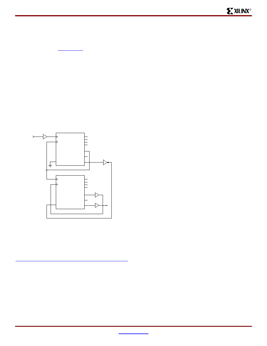
VirtexTM-E 1.8 V Field Programmable Gate Arrays
R
Module 2 of 4
www.xilinx.com
DS022-2 (v2.6) November 19, 2002
24
1-800-255-7778
Production Product Specification
Because any single DLL can access only two BUFGs at
most, any additional output clock signals must be routed
from the DLL in this example on the high speed backbone
routing.
The dll_2x files in the
xapp132.zip
file show the VHDL and
Verilog implementation of this circuit.
Virtex-E 4x Clock
Two DLLs located in the same half-edge (top-left, top-right,
bottom-right, bottom-left) can be connected together, with-
out using a BUFG between the CLKDLLs, to generate a 4x
clock as shown in
Figure 30
. Virtex-E devices, like the Virtex
devices, have four clock networks that are available for inter-
nal de-skewing of the clock. Each of the eight DLLs have
access to two of the four clock networks. Although all the
DLLs can be used for internal de-skewing, the presence of
two GCLKBUFs on the top and two on the bottom indicate
that only two of the four DLLs on the top (and two of the four
DLLs on the bottom) can be used for this purpose.
The dll_4xe files in the xapp132.zip file show the DLL imple-
mentation in Verilog for Virtex-E devices. These files can be
found at:
ftp://ftp.xilinx.com/pub/applications/xapp/xapp132.zip
Using Block SelectRAM+ Features
The Virtex FPGA Series provides dedicated blocks of
on-chip, true dual-read/write port synchronous RAM, with
4096 memory cells. Each port of the block SelectRAM+
memory can be independently configured as a read/write
port, a read port, a write port, and can be configured to a
specific data width. The block SelectRAM+ memory offers
new capabilities allowing the FPGA designer to simplify
designs.
Operating Modes
VIrtex-E block SelectRAM+ memory supports two operating
modes:
∑
Read Through
∑
Write Back
Read Through (one clock edge)
The read address is registered on the read port clock edge
and data appears on the output after the RAM access time.
Some memories might place the latch/register at the out-
puts, depending on whether a faster clock-to-out versus
set-up time is desired. This is generally considered to be an
inferior solution, since it changes the read operation to an
asynchronous function with the possibility of missing an
address/control line transition during the generation of the
read pulse clock.
Write Back (one clock edge)
The write address is registered on the write port clock edge
and the data input is written to the memory and mirrored on
the output.
Block SelectRAM+ Characteristics
∑
All inputs are registered with the port clock and have a
set-up to clock timing specification.
∑
All outputs have a read through or write back function
depending on the state of the port WE pin. The outputs
relative to the port clock are available after the
clock-to-out timing specification.
∑
The block SelectRAMs are true SRAM memories and
do not have a combinatorial path from the address to
the output. The LUT SelectRAM+ cells in the CLBs are
still available with this function.
∑
The ports are completely independent from each other
(i.e., clocking, control, address, read/write function, and
data width) without arbitration.
∑
A write operation requires only one clock edge.
∑
A read operation requires only one clock edge.
The output ports are latched with a self timed circuit to guar-
antee a glitch free read. The state of the output port does
not change until the port executes another read or write
operation.
Library Primitives
Figure 31
and
Figure 32
show the two generic library block
SelectRAM+ primitives.
Table 14
describes all of the avail-
able primitives for synthesis and simulation.
Figure 30: DLL Generation of 4x Clock in Virtex-E
Devices
ds022_031_041901
RST
CLKFB
CLKIN
CLKDLL-S
LOCKED
CLKDV
INV
BUFG
OBUF
IBUFG
CLK2X
CLK0
CLK90
CLK180
CLK270
RST
CLKFB
CLKIN
CLKDLL-P
LOCKED
CLKDV
CLK2X
CLK0
CLK90
CLK180
CLK270

VirtexTM-E 1.8 V Field Programmable Gate Arrays
R
DS022-2 (v2.6) November 19, 2002
www.xilinx.com
Module 2 of 4
Production Product Specification
1-800-255-7778
25
Port Signals
Each block SelectRAM+ port operates independently of the
others while accessing the same set of 4096 memory cells.
Table 15
describes the depth and width aspect ratios for the
block SelectRAM+ memory.
Clock--CLK[A|B]
Each port is fully synchronous with independent clock pins.
All port input pins have setup time referenced to the port
CLK pin. The data output bus has a clock-to-out time refer-
enced to the CLK pin.
Enable--EN[A|B]
The enable pin affects the read, write and reset functionality
of the port. Ports with an inactive enable pin keep the output
pins in the previous state and do not write data to the mem-
ory cells.
Write Enable--WE[A|B]
Activating the write enable pin allows the port to write to the
memory cells. When active, the contents of the data input
bus are written to the RAM at the address pointed to by the
address bus, and the new data also reflects on the data out
bus. When inactive, a read operation occurs and the con-
tents of the memory cells referenced by the address bus
reflect on the data out bus.
Reset--RST[A|B]
The reset pin forces the data output bus latches to zero syn-
chronously. This does not affect the memory cells of the
RAM and does not disturb a write operation on the other
port.
Address Bus--ADDR[A|B]<#:0>
The address bus selects the memory cells for read or write.
The width of the port determines the required width of this
bus as shown in
Table 15
.
Data In Bus--DI[A|B]<#:0>
The data in bus provides the new data value to be written
into the RAM. This bus and the port have the same width, as
shown in
Table 15
.
Figure 31: Dual-Port Block SelectRAM+ Memory
Figure 32: Single-Port Block SelectRAM+ Memory
Table 14: Available Library Primitives
Primitive
Port A Width
Port B Width
RAMB4_S1
RAMB4_S1_S1
RAMB4_S1_S2
RAMB4_S1_S4
RAMB4_S1_S8
RAMB4_S1_S16
1
N/A
1
2
4
8
16
RAMB4_S2
RAMB4_S2_S2
RAMB4_S2_S4
RAMB4_S2_S8
RAMB4_S2_S16
2
N/A
2
4
8
16
RAMB4_S4
RAMB4_S4_S4
RAMB4_S4_S8
RAMB4_S4_S16
4
N/A
4
8
16
RAMB4_S8
RAMB4_S8_S8
RAMB4_S8_S16
8
N/A
8
16
RAMB4_S16
RAMB4_S16_S16
16
N/A
16
WEB
ENB
RSTB
CLKB
ADDRB[#:0]
DIB[#:0]
WEA
ENA
RSTA
CLKA
ADDRA[#:0]
DIA[#:0]
DOA[#:0]
DOB[#:0]
RAMB4_S#_S#
ds022_032_121399
ds022_033_121399
DO[#:0]
WE
EN
RST
CLK
ADDR[#:0]
DI[#:0]
RAMB4_S#
Table 15: Block SelectRAM+ Port Aspect Ratios
Width
Depth
ADDR Bus
Data Bus
1
4096
ADDR<11:0>
DATA<0>
2
2048
ADDR<10:0>
DATA<1:0>
4
1024
ADDR<9:0>
DATA<3:0>
8
512
ADDR<8:0>
DATA<7:0>
16
256
ADDR<7:0>
DATA<15:0>

VirtexTM-E 1.8 V Field Programmable Gate Arrays
R
Module 2 of 4
www.xilinx.com
DS022-2 (v2.6) November 19, 2002
26
1-800-255-7778
Production Product Specification
Data Output Bus--DO[A|B]<#:0>
The data out bus reflects the contents of the memory cells
referenced by the address bus at the last active clock edge.
During a write operation, the data out bus reflects the data
in bus. The width of this bus equals the width of the port.
The allowed widths appear in
Table 15
.
Inverting Control Pins
The four control pins (CLK, EN, WE and RST) for each port
have independent inversion control as a configuration
option.
Address Mapping
Each port accesses the same set of 4096 memory cells
using an addressing scheme dependent on the width of the
port.
The physical RAM location addressed for a particular width
are described in the following formula (of interest only when
the two ports use different aspect ratios).
Start = ((ADDR
port
+1) * Width
port
) ≠1
End = ADDR
port
* Width
port
Table 16
shows low order address mapping for each port
width.
Creating Larger RAM Structures
The block SelectRAM+ columns have specialized routing to
allow cascading blocks together with minimal routing delays.
This achieves wider or deeper RAM structures with a smaller
timing penalty than when using normal routing channels.
Location Constraints
Block SelectRAM+ instances can have LOC properties
attached to them to constrain the placement. The block
SelectRAM+ placement locations are separate from the
CLB location naming convention, allowing the LOC proper-
ties to transfer easily from array to array.
The LOC properties use the following form.
LOC = RAMB4_R#C#
RAMB4_R0C0 is the upper left RAMB4 location on the
device.
Conflict Resolution
The block SelectRAM+ memory is a true dual-read/write
port RAM that allows simultaneous access of the same
memory cell from both ports. When one port writes to a
given memory cell, the other port must not address that
memory cell (for a write or a read) within the clock-to-clock
setup window. The following lists specifics of port and mem-
ory cell write conflict resolution.
∑
If both ports write to the same memory cell
simultaneously, violating the clock-to-clock setup
requirement, consider the data stored as invalid.
∑
If one port attempts a read of the same memory cell
the other simultaneously writes, violating the
clock-to-clock setup requirement, the following occurs.
-
The write succeeds
-
The data out on the writing port accurately reflects
the data written.
-
The data out on the reading port is invalid.
Conflicts do not cause any physical damage.
Single Port Timing
Figure 33
shows a timing diagram for a single port of a block
SelectRAM+ memory. The block SelectRAM+ AC switching
characteristics are specified in the data sheet. The block
SelectRAM+ memory is initially disabled.
At the first rising edge of the CLK pin, the ADDR, DI, EN,
WE, and RST pins are sampled. The EN pin is High and the
WE pin is Low indicating a read operation. The DO bus con-
tains the contents of the memory location, 0x00, as indi-
cated by the ADDR bus.
At the second rising edge of the CLK pin, the ADDR, DI, EN,
WR, and RST pins are sampled again. The EN and WE pins
are High indicating a write operation. The DO bus mirrors the
DI bus. The DI bus is written to the memory location 0x0F.
At the third rising edge of the CLK pin, the ADDR, DI, EN,
WR, and RST pins are sampled again. The EN pin is High
and the WE pin is Low indicating a read operation. The DO
bus contains the contents of the memory location 0x7E as
indicated by the ADDR bus.
At the fourth rising edge of the CLK pin, the ADDR, DI, EN,
WR, and RST pins are sampled again. The EN pin is Low
Table 16: Port Address Mapping
Port
Width
Port
Addresses
1
4095...
1
5
1
4
1
3
1
2
1
1
1
0
0
9
0
8
0
7
0
6
0
5
0
4
0
3
0
2
0
1
0
0
2
2047...
07
06
05
04
03
02
01
00
4
1023...
03
02
01
00
8
511...
01
00
16
255...
00
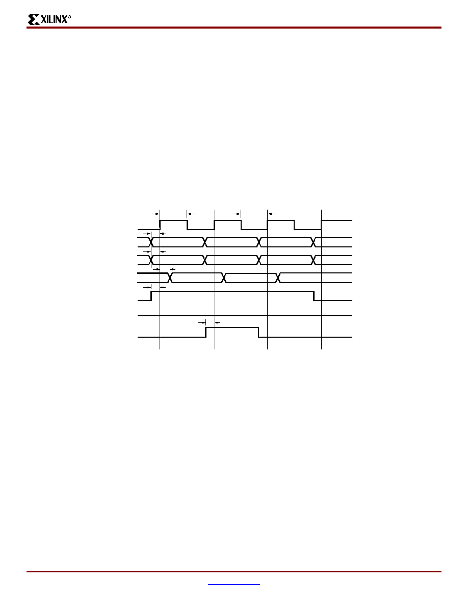
VirtexTM-E 1.8 V Field Programmable Gate Arrays
R
DS022-2 (v2.6) November 19, 2002
www.xilinx.com
Module 2 of 4
Production Product Specification
1-800-255-7778
27
indicating that the block SelectRAM+ memory is now dis-
abled. The DO bus retains the last value.
Dual Port Timing
Figure 34
shows a timing diagram for a true dual-port
read/write block SelectRAM+ memory. The clock on port A
has a longer period than the clock on Port B. The timing
parameter T
BCCS
, (clock-to-clock set-up) is shown on this
diagram. The parameter, T
BCCS
is violated once in the dia-
gram. All other timing parameters are identical to the single
port version shown in
Figure 33
.
T
BCCS
is only of importance when the address of both ports
are the same and at least one port is performing a write
operation. When the clock-to-clock set-up parameter is vio-
lated for a WRITE-WRITE condition, the contents of the
memory at that location are invalid. When the clock-to-clock
set-up parameter is violated for a WRITE-READ condition,
the contents of the memory are correct, but the read port
has invalid data.
At the first rising edge of the CLKA, memory location 0x00 is
to be written with the value 0xAAAA and is mirrored on the
DOA bus. The last operation of Port B was a read to the
same memory location 0x00. The DOB bus of Port B does
not change with the new value on Port A, and retains the
last read value. A short time later, Port B executes another
read to memory location 0x00, and the DOB bus now
reflects the new memory value written by Port A.
At the second rising edge of CLKA, memory location 0x7E
is written with the value 0x9999 and is mirrored on the DOA
bus. Port B then executes a read operation to the same
memory location without violating the T
BCCS
parameter and
the DOB reflects the new memory values written by Port A.
Figure 33: Timing Diagram for Single Port Block SelectRAM+ Memory
ds022_0343_121399
CLK
T
BPWH
T
BACK
ADDR
00
DDDD
MEM (00)
CCCC
MEM (7E)
0F
CCCC
7E
8F
BBBB
2222
DIN
DOUT
EN
RST
WE
DISABLED
READ
WRITE
READ
DISABLED
T
BDCK
T
BECK
T
BWCK
T
BCKO
T
BPWL
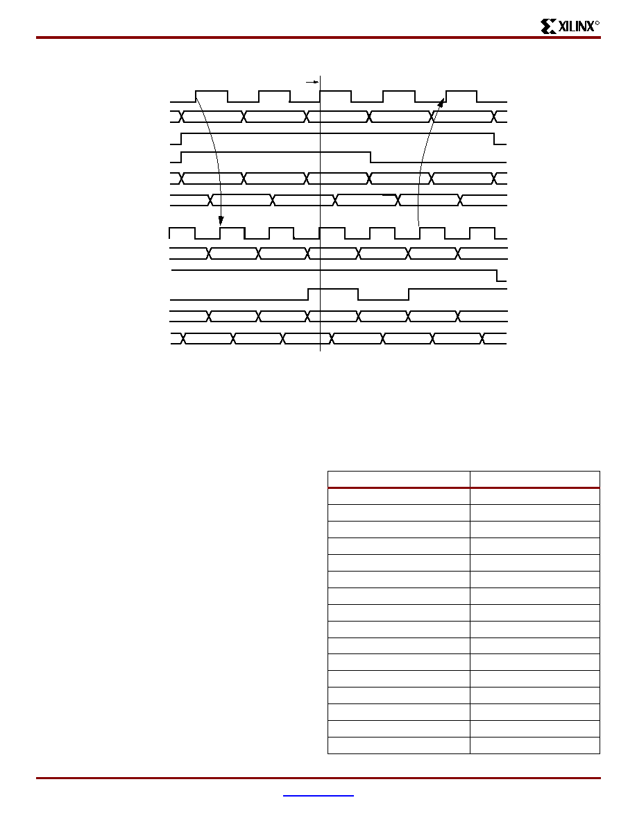
VirtexTM-E 1.8 V Field Programmable Gate Arrays
R
Module 2 of 4
www.xilinx.com
DS022-2 (v2.6) November 19, 2002
28
1-800-255-7778
Production Product Specification
At the third rising edge of CLKA, the T
BCCS
parameter is
violated with two writes to memory location 0x0F. The DOA
and DOB busses reflect the contents of the DIA and DIB
busses, but the stored value at 0x0F is invalid.
At the fourth rising edge of CLKA, a read operation is per-
formed at memory location 0x0F and invalid data is present
on the DOA bus. Port B also executes a read operation to
memory location 0x0F and also reads invalid data.
At the fifth rising edge of CLKA a read operation is per-
formed that does not violate the T
BCCS
parameter to the
previous write of 0x7E by Port B. THe DOA bus reflects the
recently written value by Port B.
Initialization
The block SelectRAM+ memory can initialize during the
device configuration sequence. The 16 initialization properties
of 64 hex values each (a total of 4096 bits) set the initialization
of each RAM. These properties appear in
Table 17
. Any initial-
ization properties not explicitly set configure as zeros. Partial
initialization strings pad with zeros. Initialization strings
greater than 64 hex values generate an error. The RAMs can
be simulated with the initialization values using generics in
VHDL simulators and parameters in Verilog simulators.
Initialization in VHDL and Synopsys
The block SelectRAM+ structures can be initialized in VHDL
for both simulation and synthesis for inclusion in the EDIF
output file. The simulation of the VHDL code uses a generic
to pass the initialization. Synopsys FPGA compiler does not
presently support generics. The initialization values instead
attach as attributes to the RAM by a built-in Synopsys
dc_script. The translate_off statement stops synthesis
translation of the generic statements. The following code
illustrates a module that employs these techniques.
Figure 34: Timing Diagram for a True Dual-port Read/Write Block SelectRAM+ Memory
ds022_035_121399
CLK_A
PORT A
PORT B
ADDR_A
00
7E
0F
00
00
7E
7E
1A
0F
0F
0F
7E
AAAA
9999
AAAA
0000
1111
2222
AAAA
9999
AAAA
UNKNOWN
EN_A
WE_A
DI_A
DO_A
1111
1111
1111
2222
FFFF
BBBB
1111
AAAA
MEM (00)
9999
2222
FFFF
BBBB
UNKNOWN
CLK_B
ADDR_B
EN_B
WE_B
DI_B
DO_B
T
BCCS
VIOLATION
T
BCCS
T
BCCS
Table 17: RAM Initialization Properties
Property
Memory Cells
INIT_00
255 to 0
INIT_01
511 to 256
INIT_02
767 to 512
INIT_03
1023 to 768
INIT_04
1279 to 1024
INIT_05
1535 to 1280
INIT_06
1791 to 2047
INIT_07
2047 to 1792
INIT_08
2303 to 2048
INIT_09
2559 to 2304
INIT_0a
2815 to 2560
INIT_0b
3071 to 2816
INIT_0c
3327 to 3072
INIT_0d
3583 to 3328
INIT_0e
3839 to 3584
INIT_0f
4095 to 3840
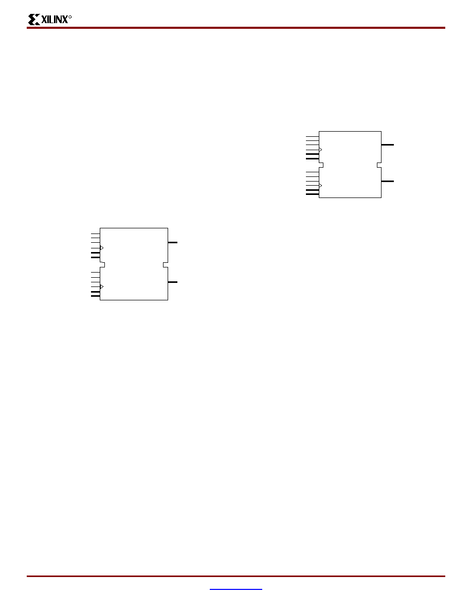
VirtexTM-E 1.8 V Field Programmable Gate Arrays
R
DS022-2 (v2.6) November 19, 2002
www.xilinx.com
Module 2 of 4
Production Product Specification
1-800-255-7778
29
Initialization in Verilog and Synopsys
The block SelectRAM+ structures can be initialized in Verilog
for both simulation and synthesis for inclusion in the EDIF
output file. The simulation of the Verilog code uses a def-
param to pass the initialization. The Synopsys FPGA com-
piler does not presently support defparam. The initialization
values instead attach as attributes to the RAM by a built-in
Synopsys dc_script. The translate_off statement stops syn-
thesis translation of the defparam statements. The following
code illustrates a module that employs these techniques.
Design Examples
Creating a 32-bit Single-Port RAM
The true dual-read/write port functionality of the block
SelectRAM+ memory allows a single port, 128 deep by
32-bit wide RAM to be created using a single block
SelectRAM+ cell as shown in
Figure 35
.
Interleaving the memory space, setting the LSB of the
address bus of Port A to 1 (V
CC
), and the LSB of the
address bus of Port B to 0 (GND), allows a 32-bit wide sin-
gle port RAM to be created.
Creating Two Single-Port RAMs
The true dual-read/write port functionality of the block
SelectRAM+ memory allows a single RAM to be split into
two single port memories of 2K bits each as shown in
Figure 36
.
In this example, a 512K x 4 RAM (Port A) and a 128 x 16
RAM (Port B) are created out of a single block SelectRAM+.
The address space for the RAM is split by fixing the MSB of
Port A to 1 (V
CC
) for the upper 2K bits and the MSB of Port
B to 0 (GND) for the lower 2K bits.
Block Memory Generation
The CoreGen program generates memory structures using
the block SelectRAM+ features. This program outputs
VHDL or Verilog simulation code templates and an EDIF file
for inclusion in a design.
Figure 35: Single Port 128 x 32 RAM
WEB
ENB
RSTB
CLKB
ADDRB[7:0]
DIB[15:0]
WEA
ENA
RSTA
CLKA
ADDRA[7:0]
DIA[15:0]
ADDR[6:0], V
CC
CLK
EN
RST
WE
CLK
EN
RST
WE
DI[31:16]
ADDR[6:0], GND
DI[15:0]
DOA[15:0]
DO[31:16]
DO[15:0]
DOB[15:0]
RAMB4_S16_S16
ds022_036_121399
Figure 36: 512 x 4 RAM and 128 x 16 RAM
WEB
ENB
RSTB
CLKB
ADDRB[7:0]
DIB[15:0]
WEA
ENA
RSTA
CLKA
ADDRA[9:0]
DIA[3:0]
V
CC
, ADDR1[8:0]
DI1[3:0]
WE1
EN1
RST1
CLK1
WE2
EN2
RST2
CLK2
GND, ADDR2[6:0]
DI2[15:0]
DOA[3:0]
DO1[3:0]
DO2[15:0]
DOB[15:0]
RAMB4_S4_S16
ds022_037_121399

VirtexTM-E 1.8 V Field Programmable Gate Arrays
R
Module 2 of 4
www.xilinx.com
DS022-2 (v2.6) November 19, 2002
30
1-800-255-7778
Production Product Specification
VHDL Initialization Example
library IEEE;
use IEEE.std_logic_1164.all;
entity MYMEM is
port (CLK, WE:in std_logic;
ADDR: in std_logic_vector(8 downto 0);
DIN: in std_logic_vector(7 downto 0);
DOUT: out std_logic_vector(7 downto 0));
end MYMEM;
architecture BEHAVE of MYMEM is
signal logic0, logic1: std_logic;
component RAMB4_S8
--synopsys translate_off
generic( INIT_00,INIT_01, INIT_02, INIT_03, INIT_04, INIT_05, INIT_06, INIT_07,
INIT_08, INIT_09, INIT_0a, INIT_0b, INIT_0c, INIT_0d, INIT_0e, INIT_0f : BIT_VECTOR(255
downto 0)
:= X"0000000000000000000000000000000000000000000000000000000000000000");
--synopsys translate_on
port (WE, EN, RST, CLK: in STD_LOGIC;
ADDR: in STD_LOGIC_VECTOR(8 downto 0);
DI: in STD_LOGIC_VECTOR(7 downto 0);
DO: out STD_LOGIC_VECTOR(7 downto 0));
end component;
--synopsys dc_script_begin
--set_attribute ram0 INIT_00
"0123456789ABCDEF0123456789ABCDEF0123456789ABCDEF0123456789ABCDEF" -type string
--set_attribute ram0 INIT_01
"FEDCBA9876543210FEDCBA9876543210FEDCBA9876543210FEDCBA9876543210" -type string
--synopsys dc_script_end
begin
logic0 <='0';
logic1 <='1';
ram0: RAMB4_S8
--synopsys translate_off
generic map (
INIT_00 => X"0123456789ABCDEF0123456789ABCDEF0123456789ABCDEF0123456789ABCDEF",
INIT_01 => X"FEDCBA9876543210FEDCBA9876543210FEDCBA9876543210FEDCBA9876543210")
--synopsys translate_on
port map (WE=>WE, EN=>logic1, RST=>logic0, CLK=>CLK,ADDR=>ADDR, DI=>DIN, DO=>DOUT);
end BEHAVE;

VirtexTM-E 1.8 V Field Programmable Gate Arrays
R
DS022-2 (v2.6) November 19, 2002
www.xilinx.com
Module 2 of 4
Production Product Specification
1-800-255-7778
31
Verilog Initialization Example
module MYMEM (CLK, WE, ADDR, DIN, DOUT);
input CLK, WE;
input [8:0] ADDR;
input [7:0] DIN;
output [7:0] DOUT;
wire logic0, logic1;
//synopsys dc_script_begin
//set_attribute ram0 INIT_00
"0123456789ABCDEF0123456789ABCDEF0123456789ABCDEF0123456789ABCDEF" -type string
//set_attribute ram0 INIT_01
"FEDCBA9876543210FEDCBA9876543210FEDCBA9876543210FEDCBA9876543210" -type string
//synopsys dc_script_end
assign logic0 = 1'b0;
assign logic1 = 1'b1;
RAMB4_S8 ram0 (.WE(WE), .EN(logic1), .RST(logic0), .CLK(CLK), .ADDR(ADDR), .DI(DIN),
.DO(DOUT));
//synopsys translate_off
defparam ram0.INIT_00 =
256h'0123456789ABCDEF0123456789ABCDEF0123456789ABCDEF0123456789ABCDEF;
defparam ram0.INIT_01 =
256h'FEDCBA9876543210FEDCBA9876543210FEDCBA9876543210FEDCBA9876543210;
//synopsys translate_on
endmodule
Using SelectI/O
The Virtex-E FPGA series includes a highly configurable,
high-performance I/O resource, called SelectI/OTM to pro-
vide support for a wide variety of I/O standards. The
SelectI/O resource is a robust set of features including pro-
grammable control of output drive strength, slew rate, and
input delay and hold time. Taking advantage of the flexibility
and SelectI/O features and the design considerations
described in this document can improve and simplify sys-
tem level design.
Introduction
As FPGAs continue to grow in size and capacity, the larger
and more complex systems designed for them demand an
increased variety of I/O standards. Furthermore, as system
clock speeds continue to increase, the need for high perfor-
mance I/O becomes more important.
While chip-to-chip delays have an increasingly substantial
impact on overall system speed, the task of achieving the
desired system performance becomes more difficult with
the proliferation of low-voltage I/O standards. SelectI/O, the
revolutionary input/output resources of Virtex-E devices,
resolve this potential problem by providing a highly config-
urable, high-performance alternative to the I/O resources of
more conventional programmable devices. Virtex-E SelectI/O
features combine the flexibility and time-to-market advan-
tages of programmable logic with the high performance pre-
viously available only with ASICs and custom ICs.
Each SelectI/O block can support up to 20 I/O standards.
Supporting such a variety of I/O standards allows the sup-
port of a wide variety of applications, from general purpose
standard applications to high-speed low-voltage memory
busses.
SelectI/O blocks also provide selectable output drive
strengths and programmable slew rates for the LVTTL out-
put buffers, as well as an optional, programmable weak
pull-up, weak pull-down, or weak "keeper" circuit ideal for
use in external bussing applications.
Each Input/Output Block (IOB) includes three registers, one
each for the input, output, and 3-state signals within the
IOB. These registers are optionally configurable as either a
D-type flip-flop or as a level sensitive latch.
The input buffer has an optional delay element used to guar-
antee a zero hold time requirement for input signals regis-
tered within the IOB.
The Virtex-E SelectI/O features also provide dedicated
resources for input reference voltage (V
REF
) and output
source voltage (V
CCO
), along with a convenient banking
system that simplifies board design.
By taking advantage of the built-in features and wide variety
of I/O standards supported by the SelectI/O features, sys-
tem-level design and board design can be greatly simplified
and improved.

VirtexTM-E 1.8 V Field Programmable Gate Arrays
R
Module 2 of 4
www.xilinx.com
DS022-2 (v2.6) November 19, 2002
32
1-800-255-7778
Production Product Specification
Fundamentals
Modern bus applications, pioneered by the largest and most
influential companies in the digital electronics industry, are
commonly introduced with a new I/O standard tailored spe-
cifically to the needs of that application. The bus I/O stan-
dards provide specifications to other vendors who create
products designed to interface with these applications.
Each standard often has its own specifications for current,
voltage, I/O buffering, and termination techniques.
The ability to provide the flexibility and time-to-market
advantages of programmable logic is increasingly depen-
dent on the capability of the programmable logic device to
support an ever increasing variety of I/O standards
The SelectI/O resources feature highly configurable input
and output buffers which provide support for a wide variety
of I/O standards. As shown in
Table 18
, each buffer type can
support a variety of voltage requirements.
Overview of Supported I/O Standards
This section provides a brief overview of the I/O standards
supported by all Virtex-E devices.
While most I/O standards specify a range of allowed volt-
ages, this document records typical voltage values only.
Detailed information on each specification can be found on
the Electronic Industry Alliance Jedec website at:
http://www.jedec.org
LVTTL -- Low-Voltage TTL
The Low-Voltage TTL, or LVTTL standard is a general pur-
pose EIA/JESDSA standard for 3.3V applications that uses
an LVTTL input buffer and a Push-Pull output buffer. This
standard requires a 3.3V output source voltage (V
CCO
), but
does not require the use of a reference voltage (V
REF
) or a
termination voltage (V
TT
).
LVCMOS2 -- Low-Voltage CMOS for 2.5 Volts
The Low-Voltage CMOS for 2.5 Volts or lower, or LVCMOS2
standard is an extension of the LVCMOS standard
(JESD 8.-5) used for general purpose 2.5V applications.
This standard requires a 2.5V output source voltage
(V
CCO
), but does not require the use of a reference voltage
(V
REF
) or a board termination voltage (V
TT
).
LVCMOS18
-- 1.8 V Low Voltage CMOS
This standard is an extension of the LVCMOS standard. It is
used in general purpose 1.8 V applications. The use of a
reference voltage (V
REF
) or a board termination voltage
(V
TT
) is not required.
PCI -- Peripheral Component Interface
The Peripheral Component Interface, or PCI standard spec-
ifies support for both 33 MHz and 66 MHz PCI bus applica-
tions. It uses a LVTTL input buffer and a Push-Pull output
buffer. This standard does not require the use of a reference
voltage (V
REF
) or a board termination voltage (V
TT
), how-
ever, it does require a 3.3V output source voltage (V
CCO
).
GTL -- Gunning Transceiver Logic Terminated
The Gunning Transceiver Logic, or GTL standard is a
high-speed bus standard (JESD8.3) invented by Xerox. Xil-
inx has implemented the terminated variation for this stan-
dard. This standard requires a differential amplifier input
buffer and a Open Drain output buffer.
GTL+ -- Gunning Transceiver Logic Plus
The Gunning Transceiver Logic Plus, or GTL+ standard is a
high-speed bus standard (JESD8.3) first used by the Pen-
tium Pro processor.
HSTL -- High-Speed Transceiver Logic
The High-Speed Transceiver Logic, or HSTL standard is a
general purpose high-speed, 1.5V bus standard sponsored
by IBM (EIA/JESD 8-6). This standard has four variations or
classes. SelectI/O devices support Class I, III, and IV. This
Table 18: Virtex-E Supported I/O Standards
I/O Standard
Output
V
CCO
Input
V
CCO
Input
V
REF
Board
Termination
Voltage
(V
TT
)
LVTTL
3.3
3.3
N/A
N/A
LVCMOS2
2.5
2.5
N/A
N/A
LVCMOS18
1.8
1.8
N/A
N/A
SSTL3 I & II
3.3
N/A
1.50
1.50
SSTL2 I & II
2.5
N/A
1.25
1.25
GTL
N/A
N/A
0.80
1.20
GTL+
N/A
N/A
1.0
1.50
HSTL I
1.5
N/A
0.75
0.75
HSTL III & IV
1.5
N/A
0.90
1.50
CTT
3.3
N/A
1.50
1.50
AGP-2X
3.3
N/A
1.32
N/A
PCI33_3 3.3
3.3
N/A
N/A
PCI66_3 3.3
3.3
N/A
N/A
BLVDS & LVDS
2.5
N/A
N/A
N/A
LVPECL
3.3
N/A
N/A
N/A

VirtexTM-E 1.8 V Field Programmable Gate Arrays
R
DS022-2 (v2.6) November 19, 2002
www.xilinx.com
Module 2 of 4
Production Product Specification
1-800-255-7778
33
standard requires a Differential Amplifier input buffer and a
Push-Pull output buffer.
SSTL3 -- Stub Series Terminated Logic for 3.3V
The Stub Series Terminated Logic for 3.3V, or SSTL3 stan-
dard is a general purpose 3.3V memory bus standard also
sponsored by Hitachi and IBM (JESD8-8). This standard
has two classes, I and II. SelectI/O devices support both
classes for the SSTL3 standard. This standard requires a
Differential Amplifier input buffer and an Push-Pull output
buffer.
SSTL2 -- Stub Series Terminated Logic for 2.5V
The Stub Series Terminated Logic for 2.5V, or SSTL2 stan-
dard is a general purpose 2.5V memory bus standard spon-
sored by Hitachi and IBM (JESD8-9). This standard has two
classes, I and II. SelectI/O devices support both classes for
the SSTL2 standard. This standard requires a Differential
Amplifier input buffer and an Push-Pull output buffer.
CTT -- Center Tap Terminated
The Center Tap Terminated, or CTT standard is a 3.3V
memory bus standard sponsored by Fujitsu (JESD8-4).
This standard requires a Differential Amplifier input buffer
and a Push-Pull output buffer.
AGP-2X -- Advanced Graphics Port
The Intel AGP standard is a 3.3V Advanced Graphics
Port-2X bus standard used with the Pentium II processor for
graphics applications. This standard requires a Push-Pull
output buffer and a Differential Amplifier input buffer.
LVDS
-- Low Voltage Differential Signal
LVDS is a differential I/O standard. It requires that one data
bit is carried through two signal lines. As with all differential
signaling standards, LVDS has an inherent noise immunity
over single-ended I/O standards. The voltage swing
between two signal lines is approximately 350mV. The use
of a reference voltage (V
REF
) or a board termination voltage
(V
TT
) is not required. LVDS requires the use of two pins per
input or output. LVDS requires external resistor termination.
BLVDS
-- Bus LVDS
This standard allows for bidirectional LVDS communication
between two or more devices. The external resistor termi-
nation is different than the one for standard LVDS.
LVPECL
-- Low Voltage Positive Emitter Coupled
Logic
LVPECL is another differential I/O standard. It requires two
signal lines for transmitting one data bit. This standard
specifies two pins per input or output. The voltage swing
between these two signal lines is approximately 850 mV.
The use of a reference voltage (V
REF
) or a board termina-
tion voltage (V
TT
) is not required. The LVPECL standard
requires external resistor termination.
Library Symbols
The Xilinx library includes an extensive list of symbols
designed to provide support for the variety of SelectI/O fea-
tures. Most of these symbols represent variations of the five
generic SelectI/O symbols.
∑
IBUF (input buffer)
∑
IBUFG (global clock input buffer)
∑
OBUF (output buffer)
∑
OBUFT (3-state output buffer)
∑
IOBUF (input/output buffer)
IBUF
Signals used as inputs to the Virtex-E device must source
an input buffer (IBUF) via an external input port. The generic
Virtex-E IBUF symbol appears in
Figure 37
. The extension
to the base name defines which I/O standard the IBUF
uses. The assumed standard is LVTTL when the generic
IBUF has no specified extension.
The following list details the variations of the IBUF symbol:
∑
IBUF
∑
IBUF_LVCMOS2
∑
IBUF_PCI33_3
∑
IBUF_PCI66_3
∑
IBUF_GTL
∑
IBUF_GTLP
∑
IBUF_HSTL_I
∑
IBUF_HSTL_III
∑
IBUF_HSTL_IV
∑
IBUF_SSTL3_I
∑
IBUF_SSTL3_II
∑
IBUF_SSTL2_I
∑
IBUF_SSTL2_II
∑
IBUF_CTT
∑
IBUF_AGP
∑
IBUF_LVCMOS18
∑
IBUF_LVDS
∑
IBUF_LVPECL
When the IBUF symbol supports an I/O standard that
requires a V
REF
, the IBUF automatically configures as a dif-
ferential amplifier input buffer. The V
REF
voltage must be
supplied on the V
REF
pins. In the case of LVDS, LVPECL,
and BLVDS, V
REF
is not required.
Figure 37: Input Buffer (IBUF) Symbols
O
I
IBUF
x133_01_111699
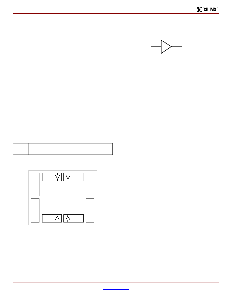
VirtexTM-E 1.8 V Field Programmable Gate Arrays
R
Module 2 of 4
www.xilinx.com
DS022-2 (v2.6) November 19, 2002
34
1-800-255-7778
Production Product Specification
The voltage reference signal is "banked" within the Virtex-E
device on a half-edge basis such that for all packages there
are eight independent V
REF
banks internally. See
Figure 38
for a representation of the Virtex-E I/O banks. Within each
bank approximately one of every six I/O pins is automati-
cally configured as a V
REF
input. After placing a differential
amplifier input signal within a given V
REF
bank, the same
external source must drive all I/O pins configured as a V
REF
input.
IBUF placement restrictions require that any differential
amplifier input signals within a bank be of the same stan-
dard. How to specify a specific location for the IBUF via the
LOC property is described below.
Table 19
summarizes the
Virtex-E input standards compatibility requirements.
An optional delay element is associated with each IBUF.
When the IBUF drives a flip-flop within the IOB, the delay
element by default activates to ensure a zero hold-time
requirement. The NODELAY=TRUE property overrides this
default.
When the IBUF does not drive a flip-flop within the IOB, the
delay element de-activates by default to provide higher per-
formance. To delay the input signal, activate the delay ele-
ment with the DELAY=TRUE property.
IBUFG
Signals used as high fanout clock inputs to the Virtex-E
device should drive a global clock input buffer (IBUFG) via
an external input port in order to take advantage of one of
the four dedicated global clock distribution networks. The
output of the IBUFG should only drive a CLKDLL,
CLKDLLHF, or BUFG symbol. The generic Virtex-E IBUFG
symbol appears in
Figure 39
.
The extension to the base name determines which I/O stan-
dard is used by the IBUFG. With no extension specified for
the generic IBUFG symbol, the assumed standard is
LVTTL.
The following list details variations of the IBUFG symbol.
∑
IBUFG
∑
IBUFG_LVCMOS2
∑
IBUFG_PCI33_3
∑
IBUFG_PCI66_3
∑
IBUFG_GTL
∑
IBUFG_GTLP
∑
IBUFG_HSTL_I
∑
IBUFG_HSTL_III
∑
IBUFG_HSTL_IV
∑
IBUFG_SSTL3_I
∑
IBUFG_SSTL3_II
∑
IBUFG_SSTL2_I
∑
IBUFG_SSTL2_II
∑
IBUFG_CTT
∑
IBUFG_AGP
∑
IBUFG_LVCMOS18
∑
IBUFG_LVDS
∑
IBUFG_LVPECL
When the IBUFG symbol supports an I/O standard that
requires a differential amplifier input, the IBUFG automati-
cally configures as a differential amplifier input buffer. The
low-voltage I/O standards with a differential amplifier input
require an external reference voltage input V
REF
.
The voltage reference signal is "banked" within the Virtex-E
device on a half-edge basis such that for all packages there
are eight independent V
REF
banks internally. See
Figure 38
for a representation of the Virtex-E I/O banks. Within each
bank approximately one of every six I/O pins is automati-
cally configured as a V
REF
input. After placing a differential
amplifier input signal within a given V
REF
bank, the same
external source must drive all I/O pins configured as a V
REF
input.
IBUFG placement restrictions require any differential ampli-
fier input signals within a bank be of the same standard. The
LOC property can specify a location for the IBUFG.
As an added convenience, the BUFGP can be used to
instantiate a high fanout clock input. The BUFGP symbol
Table 19: Xilinx Input Standards Compatibility
Requirements
Rule 1
Standards with the same input V
CCO
, output V
CCO
,
and V
REF
can be placed within the same bank.
Figure 38: Virtex-E I/O Banks
ds022_42_012100
Bank 0
GCLK3
GCLK2
GCLK1
GCLK0
Bank 1
Bank 5
Bank 4
Virtex-E
Device
Bank 7
Bank 6
Bank 2
Bank 3
Figure 39: Virtex-E Global Clock Input Buffer (IBUFG)
Symbol
O
I
IBUFG
x133_03_111699

VirtexTM-E 1.8 V Field Programmable Gate Arrays
R
DS022-2 (v2.6) November 19, 2002
www.xilinx.com
Module 2 of 4
Production Product Specification
1-800-255-7778
35
represents a combination of the LVTTL IBUFG and BUFG
symbols, such that the output of the BUFGP can connect
directly to the clock pins throughout the design.
Unlike previous architectures, the Virtex-E BUFGP symbol
can only be placed in a global clock pad location. The LOC
property can specify a location for the BUFGP.
OBUF
An OBUF must drive outputs through an external output
port. The generic output buffer (OBUF) symbol appears in
Figure 40
.
The extension to the base name defines which I/O standard
the OBUF uses. With no extension specified for the generic
OBUF symbol, the assumed standard is slew rate limited
LVTTL with 12 mA drive strength.
The LVTTL OBUF additionally can support one of two slew
rate modes to minimize bus transients. By default, the slew
rate for each output buffer is reduced to minimize power bus
transients when switching non-critical signals.
LVTTL output buffers have selectable drive strengths.
The format for LVTTL OBUF symbol names is as follows:
OBUF_<slew_rate>_<drive_strength>
where <slew_rate> is either F (Fast) or S (Slow), and
<drive_strength> is specified in milliamps (2, 4, 6, 8, 12, 16,
or 24).
The following list details variations of the OBUF symbol.
∑
OBUF
∑
OBUF_S_2
∑
OBUF_S_4
∑
OBUF_S_6
∑
OBUF_S_8
∑
OBUF_S_12
∑
OBUF_S_16
∑
OBUF_S_24
∑
OBUF_F_2
∑
OBUF_F_4
∑
OBUF_F_6
∑
OBUF_F_8
∑
OBUF_F_12
∑
OBUF_F_16
∑
OBUF_F_24
∑
OBUF_LVCMOS2
∑
OBUF_PCI33_3
∑
OBUF_PCI66_3
∑
OBUF_GTL
∑
OBUF_GTLP
∑
OBUF_HSTL_I
∑
OBUF_HSTL_III
∑
OBUF_HSTL_IV
∑
OBUF_SSTL3_I
∑
OBUF_SSTL3_II
∑
OBUF_SSTL2_I
∑
OBUF_SSTL2_II
∑
OBUF_CTT
∑
OBUF_AGP
∑
OBUF_LVCMOS18
∑
OBUF_LVDS
∑
OBUF_LVPECL
The Virtex-E series supports eight banks for the HQ and PQ
packages. The CS packages support four V
CCO
banks.
OBUF placement restrictions require that within a given
V
CCO
bank each OBUF share the same output source drive
voltage. Input buffers of any type and output buffers that do
not require V
CCO
can be placed within any V
CCO
bank.
Table 20
summarizes the Virtex-E output compatibility
requirements. The LOC property can specify a location for
the OBUF.
OBUFT
The generic 3-state output buffer OBUFT (see
Figure 41
)
typically implements 3-state outputs or bidirectional I/O.
The extension to the base name defines which I/O standard
OBUFT uses. With no extension specified for the generic
OBUFT symbol, the assumed standard is slew rate limited
LVTTL with 12 mA drive strength.
The LVTTL OBUFT additionally can support one of two slew
rate modes to minimize bus transients. By default, the slew
rate for each output buffer is reduced to minimize power bus
transients when switching non-critical signals.
Figure 40: Virtex-E Output Buffer (OBUF) Symbol
O
I
OBUF
x133_04_111699
Table 20: Output Standards Compatibility
Requirements
Rule 1
Only outputs with standards that share compatible
V
CCO
can be used within the same bank.
Rule 2
There are no placement restrictions for outputs
with standards that do not require a V
CCO
.
V
CCO
Compatible Standards
3.3
LVTTL, SSTL3_I, SSTL3_II, CTT, AGP, GTL,
GTL+, PCI33_3, PCI66_3
2.5
SSTL2_I, SSTL2_II, LVCMOS2, GTL, GTL+
1.5
HSTL_I, HSTL_III, HSTL_IV, GTL, GTL+
VirtexTM-E 1.8 V Field Programmable Gate Arrays
R
Module 2 of 4
www.xilinx.com
DS022-2 (v2.6) November 19, 2002
36
1-800-255-7778
Production Product Specification
LVTTL 3-state output buffers have selectable drive
strengths.
The format for LVTTL OBUFT symbol names is as follows:
OBUFT_<slew_rate>_<drive_strength>
where <slew_rate> is either F (Fast) or S (Slow), and
<drive_strength> is specified in milliamps (2, 4, 6, 8, 12, 16,
or 24).
The following list details variations of the OBUFT symbol.
∑
OBUFT
∑
OBUFT_S_2
∑
OBUFT_S_4
∑
OBUFT_S_6
∑
OBUFT_S_8
∑
OBUFT_S_12
∑
OBUFT_S_16
∑
OBUFT_S_24
∑
OBUFT_F_2
∑
OBUFT_F_4
∑
OBUFT_F_6
∑
OBUFT_F_8
∑
OBUFT_F_12
∑
OBUFT_F_16
∑
OBUFT_F_24
∑
OBUFT_LVCMOS2
∑
OBUFT_PCI33_3
∑
OBUFT_PCI66_3
∑
OBUFT_GTL
∑
OBUFT_GTLP
∑
OBUFT_HSTL_I
∑
OBUFT_HSTL_III
∑
OBUFT_HSTL_IV
∑
OBUFT_SSTL3_I
∑
OBUFT_SSTL3_II
∑
OBUFT_SSTL2_I
∑
OBUFT_SSTL2_II
∑
OBUFT_CTT
∑
OBUFT_AGP
∑
OBUFT_LVCMOS18
∑
OBUFT_LVDS
∑
OBUFT_LVPECL
The Virtex-E series supports eight banks for the HQ and PQ
packages. The CS package supports four V
CCO
banks.
The SelectI/O OBUFT placement restrictions require that
within a given V
CCO
bank each OBUFT share the same out-
put source drive voltage. Input buffers of any type and out-
put buffers that do not require V
CCO
can be placed within
the same V
CCO
bank.
The LOC property can specify a location for the OBUFT.
3-state output buffers and bidirectional buffers can have
either a weak pull-up resistor, a weak pull-down resistor, or
a weak "keeper" circuit. Control this feature by adding the
appropriate symbol to the output net of the OBUFT (PUL-
LUP, PULLDOWN, or KEEPER).
The weak "keeper" circuit requires the input buffer within the
IOB to sample the I/O signal. So, OBUFTs programmed for
an I/O standard that requires a V
REF
have automatic place-
ment of a V
REF
in the bank with an OBUFT configured with
a weak "keeper" circuit. This restriction does not affect most
circuit design as applications using an OBUFT configured
with a weak "keeper" typically implement a bidirectional I/O.
In this case the IBUF (and the corresponding V
REF
) are
explicitly placed.
The LOC property can specify a location for the OBUFT.
IOBUF
Use the IOBUF symbol for bidirectional signals that require
both an input buffer and a 3-state output buffer with an
active high 3-state pin. The generic input/output buffer
IOBUF appears in
Figure 42
.
The extension to the base name defines which I/O standard
the IOBUF uses. With no extension specified for the generic
IOBUF symbol, the assumed standard is LVTTL input buffer
and slew rate limited LVTTL with 12 mA drive strength for
the output buffer.
The LVTTL IOBUF additionally can support one of two slew
rate modes to minimize bus transients. By default, the slew
rate for each output buffer is reduced to minimize power bus
transients when switching non-critical signals.
LVTTL bidirectional buffers have selectable output drive
strengths.
The format for LVTTL IOBUF symbol names is as follows:
IOBUF_<slew_rate>_<drive_strength>
where <slew_rate> is either F (Fast) or S (Slow), and
<drive_strength> is specified in milliamps (2, 4, 6, 8, 12, 16,
or 24).
Figure 41: 3-State Output Buffer Symbol (OBUFT)
O
I
OBUFT
x133_05_111699
T

VirtexTM-E 1.8 V Field Programmable Gate Arrays
R
DS022-2 (v2.6) November 19, 2002
www.xilinx.com
Module 2 of 4
Production Product Specification
1-800-255-7778
37
The following list details variations of the IOBUF symbol.
∑
IOBUF
∑
IOBUF_S_2
∑
IOBUF_S_4
∑
IOBUF_S_6
∑
IOBUF_S_8
∑
IOBUF_S_12
∑
IOBUF_S_16
∑
IOBUF_S_24
∑
IOBUF_F_2
∑
IOBUF_F_4
∑
IOBUF_F_6
∑
IOBUF_F_8
∑
IOBUF_F_12
∑
IOBUF_F_16
∑
IOBUF_F_24
∑
IOBUF_LVCMOS2
∑
IOBUF_PCI33_3
∑
IOBUF_PCI66_3
∑
IOBUF_GTL
∑
IOBUF_GTLP
∑
IOBUF_HSTL_I
∑
IOBUF_HSTL_III
∑
IOBUF_HSTL_IV
∑
IOBUF_SSTL3_I
∑
IOBUF_SSTL3_II
∑
IOBUF_SSTL2_I
∑
IOBUF_SSTL2_II
∑
IOBUF_CTT
∑
IOBUF_AGP
∑
IOBUF_LVCMOS18
∑
IOBUF_LVDS
∑
IOBUF_LVPECL
When the IOBUF symbol used supports an I/O standard
that requires a differential amplifier input, the IOBUF auto-
matically configures with a differential amplifier input buffer.
The low-voltage I/O standards with a differential amplifier
input require an external reference voltage input V
REF
.
The voltage reference signal is "banked" within the Virtex-E
device on a half-edge basis such that for all packages there
are eight independent V
REF
banks internally. See
Figure 38,
page 34
for a representation of the Virtex-E I/O banks.
Within each bank approximately one of every six I/O pins is
automatically configured as a V
REF
input. After placing a dif-
ferential amplifier input signal within a given V
REF
bank, the
same external source must drive all I/O pins configured as a
V
REF
input.
IOBUF placement restrictions require any differential ampli-
fier input signals within a bank be of the same standard.
The Virtex-E series supports eight banks for the HQ and PQ
packages. The CS package supports four V
CCO
banks.
Additional restrictions on the Virtex-E SelectI/O IOBUF
placement require that within a given V
CCO
bank each
IOBUF must share the same output source drive voltage.
Input buffers of any type and output buffers that do not
require V
CCO
can be placed within the same V
CCO
bank.
The LOC property can specify a location for the IOBUF.
An optional delay element is associated with the input path
in each IOBUF. When the IOBUF drives an input flip-flop
within the IOB, the delay element activates by default to
ensure a zero hold-time requirement. Override this default
with the NODELAY=TRUE property.
In the case when the IOBUF does not drive an input flip-flop
within the IOB, the delay element de-activates by default to
provide higher performance. To delay the input signal, acti-
vate the delay element with the DELAY=TRUE property.
3-state output buffers and bidirectional buffers can have
either a weak pull-up resistor, a weak pull-down resistor, or
a weak "keeper" circuit. Control this feature by adding the
appropriate symbol to the output net of the IOBUF (PUL-
LUP, PULLDOWN, or KEEPER).
SelectI/O Properties
Access to some of the SelectI/O features (for example, loca-
tion constraints, input delay, output drive strength, and slew
rate) is available through properties associated with these
features.
Input Delay Properties
An optional delay element is associated with each IBUF.
When the IBUF drives a flip-flop within the IOB, the delay
element activates by default to ensure a zero hold-time
requirement. Use the NODELAY=TRUE property to over-
ride this default.
In the case when the IBUF does not drive a flip-flop within
the IOB, the delay element by default de-activates to pro-
vide higher performance. To delay the input signal, activate
the delay element with the DELAY=TRUE property.
Figure 42: Input/Output Buffer Symbol (IOBUF)
IO
I
IOBUF
x133_06_111699
T
O

VirtexTM-E 1.8 V Field Programmable Gate Arrays
R
Module 2 of 4
www.xilinx.com
DS022-2 (v2.6) November 19, 2002
38
1-800-255-7778
Production Product Specification
IOB Flip-Flop/Latch Property
The Virtex-E series I/O Block (IOB) includes an optional
register on the input path, an optional register on the output
path, and an optional register on the 3-state control pin. The
design implementation software automatically takes advan-
tage of these registers when the following option for the Map
program is specified.
map ≠pr b <filename>
Alternatively, the IOB = TRUE property can be placed on a
register to force the mapper to place the register in an IOB.
Location Constraints
Specify the location of each SelectI/O symbol with the loca-
tion constraint LOC attached to the SelectI/O symbol. The
external port identifier indicates the value of the location
constrain. The format of the port identifier depends on the
package chosen for the specific design.
The LOC properties use the following form:
LOC=A42
LOC=P37
Output Slew Rate Property
As mentioned above, a variety of symbol names provide the
option of choosing the desired slew rate for the output buff-
ers. In the case of the LVTTL output buffers (OBUF, OBUFT,
and IOBUF), slew rate control can be alternatively pro-
gramed with the SLEW= property. By default, the slew rate
for each output buffer is reduced to minimize power bus
transients when switching non-critical signals. The SLEW=
property has one of the two following values.
SLEW=SLOW
SLEW=FAST
Output Drive Strength Property
The desired output drive strength can be additionally speci-
fied by choosing the appropriate library symbol. The Xilinx
library also provides an alternative method for specifying
this feature. For the LVTTL output buffers (OBUF, OBUFT,
and IOBUF, the desired drive strength can be specified with
the DRIVE= property. This property could have one of the
following seven values.
DRIVE=2
DRIVE=4
DRIVE=6
DRIVE=8
DRIVE=12 (Default)
DRIVE=16
DRIVE=24
Design Considerations
Reference Voltage (V
REF
) Pins
Low-voltage I/O standards with a differential amplifier input
buffer require an input reference voltage (V
REF
). Provide the
V
REF
as an external signal to the device.
The voltage reference signal is "banked" within the device on
a half-edge basis such that for all packages there are eight
independent V
REF
banks internally. See
Figure 38
for a rep-
resentation of the Virtex-E I/O banks. Within each bank
approximately one of every six I/O pins is automatically con-
figured as a V
REF
input. After placing a differential amplifier
input signal within a given V
REF
bank, the same external
source must drive all I/O pins configured as a V
REF
input.
Within each V
REF
bank, any input buffers that require a
V
REF
signal must be of the same type. Output buffers of any
type and input buffers can be placed without requiring a ref-
erence voltage within the same V
REF
bank.
Output Drive Source Voltage (V
CCO
) Pins
Many of the low voltage I/O standards supported by
SelectI/O devices require a different output drive source
voltage (V
CCO
). As a result each device can often have to
support multiple output drive source voltages.
The Virtex-E series supports eight banks for the HQ and PQ
packages. The CS package supports four V
CCO
banks.
Output buffers within a given V
CCO
bank must share the
same output drive source voltage. Input buffers for LVTTL,
LVCMOS2, LVCMOS18, PCI33_3, and PCI 66_3 use the
V
CCO
voltage for Input V
CCO
voltage.
Transmission Line Effects
The delay of an electrical signal along a wire is dominated
by the rise and fall times when the signal travels a short dis-
tance. Transmission line delays vary with inductance and
capacitance, but a well-designed board can experience
delays of approximately 180 ps per inch.
Transmission line effects, or reflections, typically start at
1.5" for fast (1.5 ns) rise and fall times. Poor (or non-exis-
tent) termination or changes in the transmission line imped-
ance cause these reflections and can cause additional
delay in longer traces. As system speeds continue to
increase, the effect of I/O delays can become a limiting fac-
tor and therefore transmission line termination becomes
increasingly more important.
Termination Techniques
A variety of termination techniques reduce the impact of
transmission line effects.
The following are output termination techniques:
∑
None
∑
Series
∑
Parallel (Shunt)
∑
Series and Parallel (Series-Shunt)
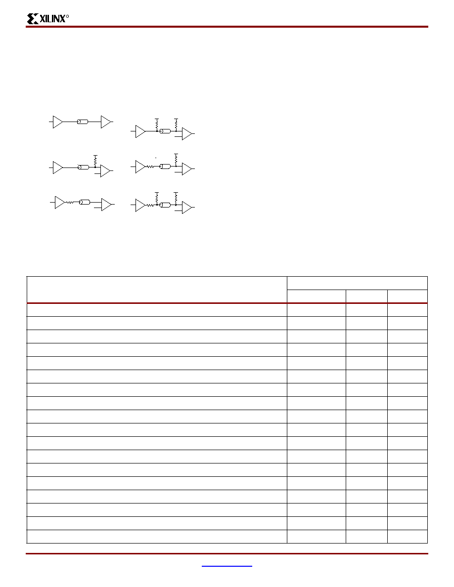
VirtexTM-E 1.8 V Field Programmable Gate Arrays
R
DS022-2 (v2.6) November 19, 2002
www.xilinx.com
Module 2 of 4
Production Product Specification
1-800-255-7778
39
Input termination techniques include the following.
∑
None
∑
Parallel (Shunt)
These termination techniques can be applied in any combi-
nation. A generic example of each combination of termina-
tion methods appears in
Figure 43
.
Simultaneous Switching Guidelines
Ground bounce can occur with high-speed digital ICs when
multiple outputs change states simultaneously, causing
undesired transient behavior on an output, or in the internal
logic. This problem is also referred to as the Simultaneous
Switching Output (SSO) problem.
Ground bounce is primarily due to current changes in the
combined inductance of ground pins, bond wires, and
ground metallization. The IC internal ground level deviates
from the external system ground level for a short duration (a
few nanoseconds) after multiple outputs change state
simultaneously.
Ground bounce affects stable Low outputs and all inputs
because they interpret the incoming signal by comparing it
to the internal ground. If the ground bounce amplitude
exceeds the actual instantaneous noise margin, then a
non-changing input can be interpreted as a short pulse with
a polarity opposite to the ground bounce.
Table 21
provides guidelines for the maximum number of
simultaneously switching outputs allowed per output
power/ground pair to avoid the effects of ground bounce. See
Table 22
for the number of effective output power/ground pairs
for each Virtex-E device and package combination.
Figure 43: Overview of Standard Input and Output
Termination Methods
x133_07_111699
Unterminated
Double Parallel Terminated
Series-Parallel Terminated Output
Driving a Parallel Terminated Input
V
TT
V
TT
V
REF
Series Terminated Output Driving
a Parallel Terminated Input
V
TT
V
REF
Unterminated Output Driving
a Parallel Terminated Input
V
TT
V
REF
V
TT
V
TT
V
REF
Series Terminated Output
V
REF
Z=50
Z=50
Z=50
Z=50
Z=50
Z=50
Table 21: Guidelines for Max Number of Simultaneously Switching Outputs per Power/Ground Pair
Standard
Package
BGA, CS, FGA
HQ
PQ, TQ
LVTTL Slow Slew Rate, 2 mA drive
68
49
36
LVTTL Slow Slew Rate, 4 mA drive
41
31
20
LVTTL Slow Slew Rate, 6 mA drive
29
22
15
LVTTL Slow Slew Rate, 8 mA drive
22
17
12
LVTTL Slow Slew Rate, 12 mA drive
17
12
9
LVTTL Slow Slew Rate, 16 mA drive
14
10
7
LVTTL Slow Slew Rate, 24 mA drive
9
7
5
LVTTL Fast Slew Rate, 2 mA drive
40
29
21
LVTTL Fast Slew Rate, 4 mA drive
24
18
12
LVTTL Fast Slew Rate, 6 mA drive
17
13
9
LVTTL Fast Slew Rate, 8 mA drive
13
10
7
LVTTL Fast Slew Rate, 12 mA drive
10
7
5
LVTTL Fast Slew Rate, 16 mA drive
8
6
4
LVTTL Fast Slew Rate, 24 mA drive
5
4
3
LVCMOS
10
7
5
PCI
8
6
4
GTL
4
4
4
GTL+
4
4
4
VirtexTM-E 1.8 V Field Programmable Gate Arrays
R
Module 2 of 4
www.xilinx.com
DS022-2 (v2.6) November 19, 2002
40
1-800-255-7778
Production Product Specification
HSTL Class I
18
13
9
HSTL Class III
9
7
5
HSTL Class IV
5
4
3
SSTL2 Class I
15
11
8
SSTL2 Class II
10
7
5
SSTL3 Class I
11
8
6
SSTL3 Class II
7
5
4
CTT
14
10
7
AGP
9
7
5
Note: This analysis assumes a 35 pF load for each output.
Table 22: Virtex-E Equivalent Power/Ground Pairs
Pkg/Part
XCV100E
XCV200E
XCV300E
XCV400E
XCV600E
XCV1000E
XCV1600E
XCV2000E
CS144
12
12
PQ240
20
20
20
20
HQ240
20
20
BG352
20
32
32
BG432
32
40
40
BG560
40
40
56
58
60
FG256
(1)
20
24
24
FG456
40
40
FG676
54
56
FG680
(2)
46
56
56
56
FG860
58
60
64
FG900
56
58
60
FG1156
96
104
120
Notes:
1.
Virtex-E devices in FG256 packages have more V
CCO
than Virtex series devices.
2.
FG680 numbers are preliminary.
Table 21: Guidelines for Max Number of Simultaneously Switching Outputs per Power/Ground Pair (Continued)
Standard
Package
BGA, CS, FGA
HQ
PQ, TQ
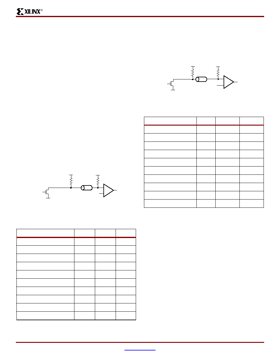
VirtexTM-E 1.8 V Field Programmable Gate Arrays
R
DS022-2 (v2.6) November 19, 2002
www.xilinx.com
Module 2 of 4
Production Product Specification
1-800-255-7778
41
Application Examples
Creating a design with the SelectI/O features requires the
instantiation of the desired library symbol within the design
code. At the board level, designers need to know the termi-
nation techniques required for each I/O standard.
This section describes some common application examples
illustrating the termination techniques recommended by
each of the standards supported by the SelectI/O features.
Termination Examples
Circuit examples involving typical termination techniques for
each of the SelectI/O standards follow. For a full range of
accepted values for the DC voltage specifications for each
standard, refer to the table associated with each figure.
The resistors used in each termination technique example
and the transmission lines depicted represent board level
components and are not meant to represent components
on the device.
GTL
A sample circuit illustrating a valid termination technique for
GTL is shown in
Figure 44
.
Table 23
lists DC voltage specifications.
GTL+
A sample circuit illustrating a valid termination technique for
GTL+ appears in
Figure 45
. DC voltage specifications
appear in
Table 24
.
Figure 44: Terminated GTL
Table 23: GTL Voltage Specifications
Parameter
Min
Typ
Max
V
CCO
-
N/A
-
V
REF
= N
◊ V
TT
1
0.74
0.8
0.86
V
TT
1.14
1.2
1.26
V
IH
= V
REF
+ 0.05
0.79
0.85
-
V
IL
= V
REF
≠ 0.05
-
0.75
0.81
V
OH
-
-
-
V
OL
-
0.2
0.4
I
OH
at V
OH
(mA)
-
-
-
I
OL
at V
OL
(mA) at 0.4V
32
-
-
I
OL
at V
OL
(mA) at 0.2V
-
-
40
Notes:
1.
N must be greater than or equal to 0.653 and less than or
equal to 0.68.
V
REF
= 0.8V
V
TT
= 1.2V
50
50
V
CCO
= N/A
Z = 50
GTL
x133_08_111699
V
TT
= 1.2V
Figure 45: Terminated GTL+
Table 24: GTL+ Voltage Specifications
Parameter
Min
Typ
Max
V
CCO
-
-
-
V
REF
= N
◊ V
TT
1
0.88
1.0
1.12
V
TT
1.35
1.5
1.65
V
IH
= V
REF
+ 0.1
0.98
1.1
-
V
IL
= V
REF
≠ 0.1
-
0.9
1.02
V
OH
-
-
-
V
OL
0.3
0.45
0.6
I
OH
at V
OH
(mA)
-
-
-
I
OL
at V
OL
(mA) at 0.6V
36
-
-
I
OL
at V
OL
(mA) at 0.3V
-
-
48
Notes:
1.
N must be greater than or equal to 0.653 and less than or
equal to 0.68.
V
REF
= 1.0V
V
TT
= 1.5V
50
V
CCO
= N/A
Z = 50
GTL+
x133_09_012400
50
V
TT
= 1.5V

VirtexTM-E 1.8 V Field Programmable Gate Arrays
R
Module 2 of 4
www.xilinx.com
DS022-2 (v2.6) November 19, 2002
42
1-800-255-7778
Production Product Specification
HSTL
A sample circuit illustrating a valid termination technique for
HSTL_I appears in
Figure 46
. A sample circuit illustrating a
valid termination technique for HSTL_III appears in
Figure 47
.
A sample circuit illustrating a valid termination technique for
HSTL_IV appears in
Figure 48
.
Table 25: HSTL Class I Voltage Specification
Parameter
Min
Typ
Max
V
CCO
1.40
1.50
1.60
V
REF
0.68
0.75
0.90
V
TT
-
V
CCO
◊ 0.5
-
V
IH
V
REF
+ 0.1
-
-
V
IL
-
-
V
REF
≠ 0.1
V
OH
V
CCO
≠ 0.4
-
-
V
OL
0.4
I
OH
at V
OH
(mA)
-8
-
-
I
OL
at V
OL
(mA)
8
-
-
Figure 46: Terminated HSTL Class I
Table 26: HSTL Class III Voltage Specification
Parameter
Min
Typ
Max
V
CCO
1.40
1.50
1.60
V
REF
(1)
-
0.90
-
V
TT
-
V
CCO
-
V
IH
V
REF
+ 0.1
-
-
V
IL
-
-
V
REF
≠ 0.1
V
OH
V
CCO
≠ 0.4
-
-
V
OL
-
-
0.4
I
OH
at V
OH
(mA)
-8
-
-
I
OL
at V
OL
(mA)
24
-
-
Note: Per EIA/JESD8-6, "The value of V
REF
is to be selected
by the user to provide optimum noise margin in the use
conditions specified by the user."
V
REF
= 0.75V
V
TT
= 0.75V
50
V
CCO
= 1.5V
Z = 50
HSTL Class I
x133_10_111699
Figure 47: Terminated HSTL Class III
Table 27: HSTL Class IV Voltage Specification
Parameter
Min
Typ
Max
V
CCO
1.40
1.50
1.60
V
REF
-
0.90
-
V
TT
-
V
CCO
-
V
IH
V
REF
+ 0.1
-
-
V
IL
-
-
V
REF
≠ 0.1
V
OH
V
CCO
≠ 0.4
-
-
V
OL
-
-
0.4
I
OH
at V
OH
(mA)
-8
-
-
I
OL
at V
OL
(mA)
48
-
-
Note: Per EIA/JESD8-6, "The value of V
REF
is to be selected
by the user to provide optimum noise margin in the use
conditions specified by the user.
Figure 48: Terminated HSTL Class IV
V
REF
= 0.9V
V
TT
= 1.5V
50
V
CCO
= 1.5V
Z = 50
HSTL Class III
x133_11_111699
50
Z = 50
HSTL Class IV
x133_12_111699
50
V
REF
= 0.9V
V
TT
= 1.5V
V
TT
= 1.5V
V
CCO
= 1.5V

VirtexTM-E 1.8 V Field Programmable Gate Arrays
R
DS022-2 (v2.6) November 19, 2002
www.xilinx.com
Module 2 of 4
Production Product Specification
1-800-255-7778
43
SSTL3_I
A sample circuit illustrating a valid termination technique for
SSTL3_I appears in
Figure 49
. DC voltage specifications
appear in
Table 28
.
SSTL3_II
A sample circuit illustrating a valid termination technique for
SSTL3_II appears in
Figure 50
. DC voltage specifications
appear in
Table 29
.
SSTL2_I
A sample circuit illustrating a valid termination technique for
SSTL2_I appears in
Figure 51
. DC voltage specifications
appear in
Table 30
.
Figure 49: Terminated SSTL3 Class I
Table 28: SSTL3_I Voltage Specifications
Parameter
Min
Typ
Max
V
CCO
3.0
3.3
3.6
V
REF
= 0.45
◊ V
CCO
1.3
1.5
1.7
V
TT
= V
REF
1.3
1.5
1.7
V
IH
= V
REF
+ 0.2
1.5
1.7
3.9
(1)
V
IL
= V
REF
≠ 0.2
-0.3
(2)
1.3
1.5
V
OH
= V
REF
+ 0.6
1.9
-
-
V
OL
= V
REF
≠ 0.6
-
-
1.1
I
OH
at V
OH
(mA)
-8
-
-
I
OL
at V
OL
(mA)
8
-
-
Notes:
1.
V
IH
maximum is V
CCO
+ 0.3
2.
V
IL
minimum does not conform to the formula
Figure 50: Terminated SSTL3 Class II
50
Z = 50
SSTL3 Class I
x133_13_111699
25
V
REF
= 1.5V
V
TT
= 1.5V
V
CCO
= 3.3V
50
Z = 50
SSTL3 Class II
x133_14_111699
25
50
V
REF
= 1.5V
V
TT
= 1.5V
V
TT
= 1.5V
V
CCO
= 3.3V
Table 29: SSTL3_II Voltage Specifications
Parameter
Min
Typ
Max
V
CCO
3.0
3.3
3.6
V
REF
= 0.45
◊ V
CCO
1.3
1.5
1.7
V
TT
= V
REF
1.3
1.5
1.7
V
IH
= V
REF
+ 0.2
1.5
1.7
3.9
(1)
V
IL
= V
REF
≠ 0.2
-0.3
(2)
1.3
1.5
V
OH
= V
REF
+ 0.8
2.1
-
-
V
OL
= V
REF
≠ 0.8
-
-
0.9
I
OH
at V
OH
(mA)
-16
-
-
I
OL
at V
OL
(mA)
16
-
-
Notes:
1.
V
IH
maximum is V
CCO
+ 0.3
2.
V
IL
minimum does not conform to the formula
Figure 51: Terminated SSTL2 Class I
Table 30: SSTL2_I Voltage Specifications
Parameter
Min
Typ
Max
V
CCO
2.3
2.5
2.7
V
REF
= 0.5
◊ V
CCO
1.15
1.25
1.35
V
TT
= V
REF
+ N
(1)
1.11
1.25
1.39
V
IH
= V
REF
+ 0.18
1.33
1.43
3.0
(2)
V
IL
= V
REF
≠ 0.18
-0.3
(3)
1.07
1.17
V
OH
= V
REF
+ 0.61
1.76
-
-
V
OL
= V
REF
≠ 0.61
-
-
0.74
I
OH
at V
OH
(mA)
-7.6
-
-
I
OL
at V
OL
(mA)
7.6
-
-
Notes:
1.
N must be greater than or equal to -0.04 and less than or
equal to 0.04.
2.
V
IH
maximum is V
CCO
+ 0.3.
3.
V
IL
minimum does not conform to the formula.
50
Z = 50
SSTL2 Class I
xap133_15_011000
25
V
REF
= 1.25V
V
TT
= 1.25V
V
CCO
= 2.5V
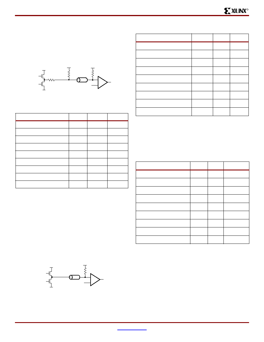
VirtexTM-E 1.8 V Field Programmable Gate Arrays
R
Module 2 of 4
www.xilinx.com
DS022-2 (v2.6) November 19, 2002
44
1-800-255-7778
Production Product Specification
SSTL2_II
A sample circuit illustrating a valid termination technique for
SSTL2_II appears in
Figure 52
. DC voltage specifications
appear in
Table 31
.
CTT
A sample circuit illustrating a valid termination technique for
CTT appear in
Figure 53
. DC voltage specifications appear
in
Table 32
.
PCI33_3 & PCI66_3
PCI33_3 or PCI66_3 require no termination. DC voltage
specifications appear in
Table 33
.
Figure 52: Terminated SSTL2 Class II
Table 31: SSTL2_II Voltage Specifications
Parameter
Min
Typ
Max
V
CCO
2.3
2.5
2.7
V
REF
= 0.5
◊ V
CCO
1.15
1.25
1.35
V
TT
= V
REF
+ N
(1)
1.11
1.25
1.39
V
IH
= V
REF
+ 0.18
1.33
1.43
3.0
(2)
V
IL
= V
REF
≠ 0.18
-0.3
(3)
1.07
1.17
V
OH
= V
REF
+ 0.8
1.95
-
-
V
OL
= V
REF
≠ 0.8
-
-
0.55
I
OH
at V
OH
(mA)
-15.2
-
-
I
OL
at V
OL
(mA)
15.2
-
-
Notes:
1.
N must be greater than or equal to -0.04 and less than or
equal to 0.04.
2.
V
IH
maximum is V
CCO
+ 0.3.
3.
V
IL
minimum does not conform to the formula.
Figure 53: Terminated CTT
50
Z = 50
SSTL2 Class II
x133_16_111699
25
50
V
REF
= 1.25V
V
TT
= 1.25V
V
TT
= 1.25V
V
CCO
= 2.5V
V
REF
= 1.5V
V
TT
= 1.5V
50
V
CCO
= 3.3V
Z = 50
CTT
x133_17_111699
Table 32: CTT Voltage Specifications
Parameter
Min
Typ
Max
V
CCO
2.05
(1)
3.3
3.6
V
REF
1.35
1.5
1.65
V
TT
1.35
1.5
1.65
V
IH
= V
REF
+ 0.2
1.55
1.7
-
V
IL
= V
REF
≠ 0.2
-
1.3
1.45
V
OH
= V
REF
+ 0.4
1.75
1.9
-
V
OL
= V
REF
≠ 0.4
-
1.1
1.25
I
OH
at V
OH
(mA)
-8
-
-
I
OL
at V
OL
(mA)
8
-
-
Notes:
1.
Timing delays are calculated based on V
CCO
min of 3.0V.
Table 33: PCI33_3 and PCI66_3 Voltage Specifications
Parameter
Min
Typ
Max
V
CCO
3.0
3.3
3.6
V
REF
-
-
-
V
TT
-
-
-
V
IH
= 0.5
◊ V
CCO
1.5
1.65
V
CCO
+ 0.5
V
IL
= 0.3
◊ V
CCO
-0.5
0.99
1.08
V
OH
= 0.9
◊ V
CCO
2.7
-
-
V
OL
= 0.1
◊ V
CCO
-
-
0.36
I
OH
at V
OH
(mA)
Note 1
-
-
I
OL
at V
OL
(mA)
Note 1
-
-
Notes:
1.
Tested according to the relevant specification.
VirtexTM-E 1.8 V Field Programmable Gate Arrays
R
DS022-2 (v2.6) November 19, 2002
www.xilinx.com
Module 2 of 4
Production Product Specification
1-800-255-7778
45
LVTTL
LVTTL requires no termination. DC voltage specifications
appears in
Table 34
.
LVCMOS2
LVCMOS2 requires no termination. DC voltage specifica-
tions appear in
Table 35
.
LVCMOS18
LVCMOS18 does not require termination.
Table 36
lists DC
voltage specifications.
AGP-2X
The specification for the AGP-2X standard does not docu-
ment a recommended termination technique. DC voltage
specifications appear in
Table 37
.
Table 34: LVTTL Voltage Specifications
Parameter
Min
Typ
Max
V
CCO
3.0
3.3
3.6
V
REF
-
-
-
V
TT
-
-
-
V
IH
2.0
-
3.6
V
IL
-0.5
-
0.8
V
OH
2.4
-
-
V
OL
-
-
0.4
I
OH
at V
OH
(mA)
-24
-
-
I
OL
at V
OL
(mA)
24
-
-
Notes:
1.
Note: V
OL
and V
OH
for lower drive currents sample tested.
Table 35: LVCMOS2 Voltage Specifications
Parameter
Min
Typ
Max
V
CCO
2.3
2.5
2.7
V
REF
-
-
-
V
TT
-
-
-
V
IH
1.7
-
3.6
V
IL
-0.5
-
0.7
V
OH
1.9
-
-
V
OL
-
-
0.4
I
OH
at V
OH
(mA)
-12
-
-
I
OL
at V
OL
(mA)
12
-
-
Table 36: LVCMOS18 Voltage Specifications
Parameter
Min
Typ
Max
V
CCO
1.70
1.80
1.90
V
REF
-
-
-
V
TT
-
-
-
V
IH
0.65 x V
CCO
-
1.95
V
IL
≠ 0.5
-
0.2 x V
CCO
V
OH
V
CCO
≠ 0.4
-
-
V
OL
-
-
0.4
I
OH
at V
OH
(mA)
≠8
-
-
I
OL
at V
OL
(mA)
8
-
-
Table 37: AGP-2X Voltage Specifications
Parameter
Min
Typ
Max
V
CCO
3.0
3.3
3.6
V
REF
= N
◊ V
CCO
(1)
1.17
1.32
1.48
V
TT
-
-
-
V
IH
= V
REF
+ 0.2
1.37
1.52
-
V
IL
= V
REF
≠ 0.2
-
1.12
1.28
V
OH
= 0.9
◊ V
CCO
2.7
3.0
-
V
OL
= 0.1
◊ V
CCO
-
0.33
0.36
I
OH
at V
OH
(mA)
Note 2
-
-
I
OL
at V
OL
(mA)
Note 2
-
-
Notes:
1.
N must be greater than or equal to 0.39 and less than or
equal to 0.41.
2.
Tested according to the relevant specification.

VirtexTM-E 1.8 V Field Programmable Gate Arrays
R
Module 2 of 4
www.xilinx.com
DS022-2 (v2.6) November 19, 2002
46
1-800-255-7778
Production Product Specification
LVDS
Depending on whether the device is transmitting an LVDS
signal or receiving an LVDS signal, there are two different
circuits used for LVDS termination. A sample circuit illustrat-
ing a valid termination technique for transmitting LVDS sig-
nals appears in
Figure 54
. A sample circuit illustrating a
valid termination for receiving LVDS signals appears in
Figure 55
.
Table 38
lists DC voltage specifications. Further
information on the specific termination resistor packs shown
can be found on
Table 40
.
LVPECL
Depending on whether the device is transmitting or receiv-
ing an LVPECL signal, two different circuits are used for
LVPECL termination. A sample circuit illustrating a valid ter-
mination technique for transmitting LVPECL signals
appears in
Figure 56
. A sample circuit illustrating a valid ter-
mination for receiving LVPECL signals appears in
Figure 57
.
Table 39
lists DC voltage specifications. Further
information on the specific termination resistor packs shown
can be found on
Table 40
.
Figure 54: Transmitting LVDS Signal Circuit
Figure 55: Receiving LVDS Signal Circuit
Table 38: LVDS Voltage Specifications
Parameter
Min
Typ
Max
V
CCO
2.375
2.5
2.625
V
ICM
(2)
0.2
1.25
2.2
V
OCM
(1)
1.125
1.25
1.375
V
IDIFF
(1)
0.1
0.35
-
V
ODIFF
(1)
0.25
0.35
0.45
V
OH
(1)
1.25
-
-
V
OL
(1)
-
-
1.25
Notes:
1.
Measured with a 100
resistor across Q and Q.
2.
Measured with a differential input voltage =
+/- 350 mV.
x133_19_122799
Q
Z0 = 50
Z0 = 50
Q
Virtex-E
FPGA
to LVDS Receiver
to LVDS Receiver
RDIV
140
R
S
165
R
S
165
2.5V
V
CCO
= 2.5V
LVDS
Output
DATA
Transmit
1/4 of Bourns
Part Number
CAT16-LV4F12
x133_29_122799
Q
Z0 = 50
LVDS_IN
LVDS_IN
Z0 = 50
R
T
100
Q
DATA
Receive
from
LVDS
Driver
VIRTEX-E
FPGA
+
≠
Table 39: LVPECL Voltage Specifications
Parameter
Min
Typ
Max
V
CCO
3.0
3.3
3.6
V
REF
-
-
-
V
TT
-
-
-
V
IH
1.49
-
2.72
V
IL
0.86
-
2.125
V
OH
1.8
-
-
V
OL
-
-
1.57
Notes:
1.
For more detailed information, see
LVPECL DC
Specifications
Figure 56: Transmitting LVPECL Signal Circuit
Figure 57: Receiving LVPECL Signal Circuit
x133_20_122799
Q
Z0 = 50 LVPECL_OUT
LVPECL_OUT
Z0 = 50
Q
Virtex-E
FPGA
to LVPECL Receiver
to LVPECL Receiver
RDIV
187
R
S
100
R
S
100
3.3V
DATA
Transmit
1/4 of Bourns
Part Number
CAT16-PC4F12
x133_21_122799
Q
Z0 = 50
LVPECL_IN
LVPECL_IN
Z0 = 50
R
T
100
Q
DATA
Receive
from
LVPECL
Driver
VIRTEX-E
FPGA
+
≠

VirtexTM-E 1.8 V Field Programmable Gate Arrays
R
DS022-2 (v2.6) November 19, 2002
www.xilinx.com
Module 2 of 4
Production Product Specification
1-800-255-7778
47
Termination Resistor Packs
Resistor packs are available with the values and the config-
uration required for LVDS and LVPECL termination from
Bourns, Inc., as listed in Table. For pricing and availability,
please contact Bourns directly at
http://www.bourns.com
.
LVDS Design Guide
The SelectI/O library elements have been expanded for Vir-
tex-E devices to include new LVDS variants. At this time all
of the cells might not be included in the Synthesis libraries.
The 2.1i-Service Pack 2 update for Alliance and Foundation
software includes these cells in the VHDL and Verilog librar-
ies. It is necessary to combine these cells to create the
P-side (positive) and N-side (negative) as described in the
input, output, 3-state and bidirectional sections.
Creating LVDS Global Clock Input Buffers
Global clock input buffers can be combined with adjacent
IOBs to form LVDS clock input buffers. P-side is the GCLK-
PAD location; N-side is the adjacent IO_LVDS_DLL site.
HDL Instantiation
Only one global clock input buffer is required to be instanti-
ated in the design and placed on the correct GCLKPAD
location. The N-side of the buffer is reserved and no other
IOB is allowed to be placed on this location.
In the physical device, a configuration option is enabled that
routes the pad wire to the differential input buffer located in
the GCLKIOB. The output of this buffer then drives the out-
put of the GCLKIOB cell. In EPIC it appears that the second
buffer is unused. Any attempt to use this location for another
purpose leads to a DRC error in the software.
VHDL Instantiation
gclk0_p : IBUFG_LVDS port map
(I=>clk_external, O=>clk_internal);
Verilog Instantiation
IBUFG_LVDS gclk0_p (.I(clk_external),
.O(clk_internal));
Location constraints
All LVDS buffers must be explicitly placed on a device. For
the global clock input buffers this can be done with the fol-
lowing constraint in the .ucf or .ncf file.
NET clk_external LOC = GCLKPAD3;
GCLKPAD3 can also be replaced with the package pin
name such as D17 for the BG432 package.
Table 40: Bourns LVDS/LVPECL Resistor Packs
Part Number
I/O Standard
Term.
for:
Pairs/
Pack
Pins
CAT16
-LV2F6
LVDS
Driver
2
8
CAT16
-LV4F12
LVDS
Driver
4
16
CAT16
-PC2F6
LVPECL
Driver
2
8
CAT16
-PC4F12
LVPECL
Driver
4
16
CAT16
-PT2F2
LVDS/LVPECL
Receiver
2
8
CAT16
-PT4F4
LVDS/LVPECL
Receiver
4
16
Figure 58: LVDS elements
O
I
IBUF_LVDS
O
I
OBUF_LVDS
IOBUF_LVDS
O
O
T
I
OBUFT_LVDS
O
I
IBUFG_LVDS
IO
T
I
x133_22_122299
Table 41: Global Clock Input Buffer Pair Locations
Pkg
GCLK 3
GCLK 2
GCLK 1
GCLK 0
P
N
P
N
P
N
P
N
CS144
A6
C6
A7
B7
M7
M6
K7
N8
PQ240
P213
P215
P210 P209
P89
P87
P92
P93
HQ240
P213
P215
P210 P209
P89
P87
P92
P93
BG352
D14
A15
B14
A13
AF14
AD14
AE13
AC13
BG432
D17
C17
A16
B16
AK16
AL17
AL16
AH15
BG560
A17
C18
D17
E17
AJ17
AM18
AL17
AM17
FG256
B8
A7
C9
A8
R8
T8
N8
N9
FG456
C11
B11
A11
D11
Yll
AA11
W12
U12
FG676
E13
B13
C13
F14
AB13
AF13
AA14
AC14
FG680
A20
C22
D21
A19
AU22
AT22
AW19
AT21
FG860
C22
A22
B22
D22
AY22
AW21
BA22
AW20
FG900
C15
A15
E15
E16
AK16
AH16
AJ16
AF16
FG1156
E17
C17
D17
J18
Al19
AL17
AH18
AM18

VirtexTM-E 1.8 V Field Programmable Gate Arrays
R
Module 2 of 4
www.xilinx.com
DS022-2 (v2.6) November 19, 2002
48
1-800-255-7778
Production Product Specification
Optional N-side
Some designers might prefer to also instantiate the N-side
buffer for the global clock buffer. This allows the top-level net
list to include net connections for both PCB layout and sys-
tem-level integration. In this case, only the output P-side
IBUFG connection has a net connected to it. Since the
N-side IBUFG does not have a connection in the EDIF net
list, it is trimmed from the design in MAP.
VHDL Instantiation
gclk0_p : IBUFG_LVDS port map
(I=>clk_p_external, O=>clk_internal);
gclk0_n : IBUFG_LVDS port map
(I=>clk_n_external, O=>clk_internal);
Verilog Instantiation
IBUFG_LVDS gclk0_p (.I(clk_p_external),
.O(clk_internal));
IBUFG_LVDS gclk0_n (.I(clk_n_external),
.O(clk_internal));
Location Constraints
All LVDS buffers must be explicitly placed on a device. For
the global clock input buffers this can be done with the fol-
lowing constraint in the .ucf or .ncf file.
NET clk_p_external LOC = GCLKPAD3;
NET clk_n_external LOC = C17;
GCLKPAD3 can also be replaced with the package pin
name, such as D17 for the BG432 package.
Creating LVDS Input Buffers
An LVDS input buffer can be placed in a wide number of IOB
locations. The exact location is dependent on the package
that is used. The Virtex-E package information lists the pos-
sible locations as IO_L#P for the P-side and IO_L#N for the
N-side where # is the pair number.
HDL Instantiation
Only one input buffer is required to be instantiated in the
design and placed on the correct IO_L#P location. The
N-side of the buffer is reserved and no other IOB is allowed
to be placed on this location. In the physical device, a con-
figuration option is enabled that routes the pad wire from the
IO_L#N IOB to the differential input buffer located in the
IO_L#P IOB. The output of this buffer then drives the output
of the IO_L#P cell or the input register in the IO_L#P IOB. In
EPIC it appears that the second buffer is unused. Any
attempt to use this location for another purpose leads to a
DRC error in the software.
VHDL Instantiation
data0_p : IBUF_LVDS port map (I=>data(0),
O=>data_int(0));
Verilog Instantiation
IBUF_LVDS data0_p (.I(data[0]),
.O(data_int[0]));
Location Constraints
All LVDS buffers must be explicitly placed on a device. For
the input buffers this can be done with the following con-
straint in the .ucf or .ncf file.
NET data<0> LOC = D28; # IO_L0P
Optional N-side
Some designers might prefer to also instantiate the N-side
buffer for the input buffer. This allows the top-level net list to
include net connections for both PCB layout and sys-
tem-level integration. In this case, only the output P-side
IBUF connection has a net connected to it. Since the N-side
IBUF does not have a connection in the EDIF net list, it is
trimmed from the design in MAP.
VHDL Instantiation
data0_p : IBUF_LVDS port map
(I=>data_p(0), O=>data_int(0));
data0_n : IBUF_LVDS port map
(I=>data_n(0), O=>open);
Verilog Instantiation
IBUF_LVDS data0_p (.I(data_p[0]),
.O(data_int[0]));
IBUF_LVDS data0_n (.I(data_n[0]), .O());
Location Constraints
All LVDS buffers must be explicitly placed on a device. For
the global clock input buffers this can be done with the fol-
lowing constraint in the .ucf or .ncf file.
NET data_p<0> LOC = D28; # IO_L0P
NET data_n<0> LOC = B29; # IO_L0N
Adding an Input Register
All LVDS buffers can have an input register in the IOB. The
input register is in the P-side IOB only. All the normal IOB
register options are available (FD, FDE, FDC, FDCE, FDP,
FDPE, FDR, FDRE, FDS, FDSE, LD, LDE, LDC, LDCE,
LDP, LDPE). The register elements can be inferred or
explicitly instantiated in the HDL code.
The register elements can be packed in the IOB using the
IOB property to TRUE on the register or by using the "map
-pr [i|o|b]" where "i" is inputs only, "o" is outputs only and "b"
is both inputs and outputs.
To improve design coding times VHDL and Verilog synthesis
macro libraries available to explicitly create these structures.
The input library macros are listed in
Table 42
. The I and IB
inputs to the macros are the external net connections.

VirtexTM-E 1.8 V Field Programmable Gate Arrays
R
DS022-2 (v2.6) November 19, 2002
www.xilinx.com
Module 2 of 4
Production Product Specification
1-800-255-7778
49
Creating LVDS Output Buffers
LVDS output buffers can be placed in a wide number of IOB
locations. The exact locations are dependent on the pack-
age used. The Virtex-E package information lists the possi-
ble locations as IO_L#P for the P-side and IO_L#N for the
N-side, where # is the pair number.
HDL Instantiation
Both output buffers are required to be instantiated in the
design and placed on the correct IO_L#P and IO_L#N loca-
tions. The IOB must have the same net source the following
pins, clock (C), set/reset (SR), output (O), output clock
enable (OCE). In addition, the output (O) pins must be
inverted with respect to each other, and if output registers
are used, the INIT states must be opposite values (one
HIGH and one LOW). Failure to follow these rules leads to
DRC errors in software.
VHDL Instantiation
data0_p : OBUF_LVDS port map
(I=>data_int(0), O=>data_p(0));
data0_inv: INV port map
(I=>data_int(0), O=>data_n_int(0));
data0_n : OBUF_LVDS port map
(I=>data_n_int(0), O=>data_n(0));
Verilog Instantiation
OBUF_LVDS data0_p (.I(data_int[0]),
.O(data_p[0]));
INV data0_inv (.I(data_int[0],
.O(data_n_int[0]);
OBUF_LVDS data0_n (.I(data_n_int[0]),
.O(data_n[0]));
Location Constraints
All LVDS buffers must be explicitly placed on a device. For
the output buffers this can be done with the following con-
straint in the .ucf or .ncf file.
NET data_p<0> LOC = D28; # IO_L0P
NET data_n<0> LOC = B29; # IO_L0N
Synchronous vs. Asynchronous Outputs
If the outputs are synchronous (registered in the IOB) then
any IO_L#P|N pair can be used. If the outputs are asynchro-
nous (no output register), then they must use one of the
pairs that are part of the same IOB group at the end of a
ROW or COLUMN in the device.
The LVDS pairs that can be used as asynchronous outputs
are listed in the Virtex-E pinout tables. Some pairs are
marked as asynchronous-capable for all devices in that
package, and others are marked as available only for that
device in the package. If the device size might change at
some point in the product lifetime, then only the common
pairs for all packages should be used.
Adding an Output Register
All LVDS buffers can have an output register in the IOB. The
output registers must be in both the P-side and N-side IOBs.
All the normal IOB register options are available (FD, FDE,
FDC, FDCE, FDP, FDPE, FDR, FDRE, FDS, FDSE, LD,
LDE, LDC, LDCE, LDP, LDPE). The register elements can
be inferred or explicitly instantiated in the HDL code.
Special care must be taken to insure that the D pins of the
registers are inverted and that the INIT states of the regis-
ters are opposite. The clock pin (C), clock enable (CE) and
set/reset (CLR/PRE or S/R) pins must connect to the same
source. Failure to do this leads to a DRC error in the soft-
ware.
The register elements can be packed in the IOB using the
IOB property to TRUE on the register or by using the "map
-pr [i|o|b]" where "i" is inputs only, "o" is outputs only and "b"
is both inputs and outputs.
To improve design coding times VHDL and Verilog synthe-
sis macro libraries have been developed to explicitly create
these structures. The output library macros are listed in
Table 43
. The O and OB inputs to the macros are the exter-
nal net connections.
Table 42: Input Library Macros
Name
Inputs
Outputs
IBUFDS_FD_LVDS
I, IB, C
Q
IBUFDS_FDE_LVDS
I, IB, CE, C
Q
IBUFDS_FDC_LVDS
I, IB, C, CLR
Q
IBUFDS_FDCE_LVDS
I, IB, CE, C, CLR
Q
IBUFDS_FDP_LVDS
I, IB, C, PRE
Q
IBUFDS_FDPE_LVDS
I, IB, CE, C, PRE
Q
IBUFDS_FDR_LVDS
I, IB, C, R
Q
IBUFDS_FDRE_LVDS
I, IB, CE, C, R
Q
IBUFDS_FDS_LVDS
I, IB, C, S
Q
IBUFDS_FDSE_LVDS
I, IB, CE, C, S
Q
IBUFDS_LD_LVDS
I, IB, G
Q
IBUFDS_LDE_LVDS
I, IB, GE, G
Q
IBUFDS_LDC_LVDS
I, IB, G, CLR
Q
IBUFDS_LDCE_LVDS
I, IB, GE, G, CLR
Q
IBUFDS_LDP_LVDS
I, IB, G, PRE
Q
IBUFDS_LDPE_LVDS
I, IB, GE, G, PRE
Q

VirtexTM-E 1.8 V Field Programmable Gate Arrays
R
Module 2 of 4
www.xilinx.com
DS022-2 (v2.6) November 19, 2002
50
1-800-255-7778
Production Product Specification
Creating LVDS Output 3-State Buffers
LVDS output 3-state buffers can be placed in a wide number
of IOB locations. The exact locations are dependent on the
package used. The Virtex-E package information lists the
possible locations as IO_L#P for the P-side and IO_L#N for
the N-side, where # is the pair number.
HDL Instantiation
Both output 3-state buffers are required to be instantiated in
the design and placed on the correct IO_L#P and IO_L#N
locations. The IOB must have the same net source the fol-
lowing pins, clock (C), set/reset (SR), 3-state (T), 3-state
clock enable (TCE), output (O), output clock enable (OCE).
In addition, the output (O) pins must be inverted with
respect to each other, and if output registers are used, the
INIT states must be opposite values (one High and one
Low). If 3-state registers are used, they must be initialized to
the same state. Failure to follow these rules leads to DRC
errors in the software.
VHDL Instantiation
data0_p: OBUFT_LVDS port map
(I=>data_int(0), T=>data_tri,
O=>data_p(0));
data0_inv: INV port map
(I=>data_int(0), O=>data_n_int(0));
data0_n: OBUFT_LVDS port map
(I=>data_n_int(0), T=>data_tri,
O=>data_n(0));
Verilog Instantiation
OBUFT_LVDS data0_p (.I(data_int[0]),
.T(data_tri), .O(data_p[0]));
INV data0_inv (.I(data_int[0],
.O(data_n_int[0]);
OBUFT_LVDS data0_n (.I(data_n_int[0]),
.T(data_tri), .O(data_n[0]));
Location Constraints
All LVDS buffers must be explicitly placed on a device. For
the output buffers this can be done with the following con-
straint in the .ucf or .ncf file.
NET data_p<0> LOC = D28; # IO_L0P
NET data_n<0> LOC = B29; # IO_L0N
Synchronous vs. Asynchronous 3-State Outputs
If the outputs are synchronous (registered in the IOB), then
any IO_L#P|N pair can be used. If the outputs are asynchro-
nous (no output register), then they must use one of the
pairs that are part of the same IOB group at the end of a
ROW or COLUMN in the device. This applies for either the
3-state pin or the data out pin.
LVDS pairs that can be used as asynchronous outputs are
listed in the Virtex-E pinout tables. Some pairs are marked
as "asynchronous capable" for all devices in that package,
and others are marked as available only for that device in
the package. If the device size might be changed at some
point in the product lifetime, then only the common pairs for
all packages should be used.
Adding Output and 3-State Registers
All LVDS buffers can have an output register in the IOB. The
output registers must be in both the P-side and N-side IOBs.
All the normal IOB register options are available (FD, FDE,
FDC, FDCE, FDP, FDPE, FDR, FDRE, FDS, FDSE, LD,
LDE, LDC, LDCE, LDP, LDPE). The register elements can
be inferred or explicitly instantiated in the HDL code.
Special care must be taken to insure that the D pins of the
registers are inverted and that the INIT states of the regis-
ters are opposite. The 3-state (T), 3-state clock enable
(CE), clock pin (C), output clock enable (CE) and set/reset
(CLR/PRE or S/R) pins must connect to the same source.
Failure to do this leads to a DRC error in the software.
Table 43: Output Library Macros
Name
Inputs
Outputs
OBUFDS_FD_LVDS
D, C
O, OB
OBUFDS_FDE_LVDS
DD, CE, C
O, OB
OBUFDS_FDC_LVDS
D, C, CLR
O, OB
OBUFDS_FDCE_LVDS
D, CE, C, CLR
O, OB
OBUFDS_FDP_LVDS
D, C, PRE
O, OB
OBUFDS_FDPE_LVDS
D, CE, C, PRE
O, OB
OBUFDS_FDR_LVDS
D, C, R
O, OB
OBUFDS_FDRE_LVDS
D, CE, C, R
O, OB
OBUFDS_FDS_LVDS
D, C, S
O, OB
OBUFDS_FDSE_LVDS
D, CE, C, S
O, OB
OBUFDS_LD_LVDS
D, G
O, OB
OBUFDS_LDE_LVDS
D, GE, G
O, OB
OBUFDS_LDC_LVDS
D, G, CLR
O, OB
OBUFDS_LDCE_LVDS
D, GE, G, CLR
O, OB
OBUFDS_LDP_LVDS
D, G, PRE
O, OB
OBUFDS_LDPE_LVDS
D, GE, G, PRE
O, OB

VirtexTM-E 1.8 V Field Programmable Gate Arrays
R
DS022-2 (v2.6) November 19, 2002
www.xilinx.com
Module 2 of 4
Production Product Specification
1-800-255-7778
51
The register elements can be packed in the IOB using the
IOB property to TRUE on the register or by using the "map
-pr [i|o|b]" where "i" is inputs only, "o" is outputs only and "b"
is both inputs and outputs.
To improve design coding times VHDL and Verilog synthe-
sis macro libraries have been developed to explicitly create
these structures. The input library macros are listed below.
The 3-state is configured to be 3-stated at GSR and when
the PRE,CLR,S or R is asserted and shares it's clock
enable with the output register. If this is not desirable then
the library can be updated by the user for the desired func-
tionality. The O and OB inputs to the macros are the exter-
nal net connections.
Creating a LVDS Bidirectional Buffer
LVDS bidirectional buffers can be placed in a wide number
of IOB locations. The exact locations are dependent on the
package used. The Virtex-E package information lists the
possible locations as IO_L#P for the P-side and IO_L#N for
the N-side, where # is the pair number.
HDL Instantiation
Both bidirectional buffers are required to be instantiated in
the design and placed on the correct IO_L#P and IO_L#N
locations. The IOB must have the same net source the fol-
lowing pins, clock (C), set/reset (SR), 3-state (T), 3-state
clock enable (TCE), output (O), output clock enable (OCE).
In addition, the output (O) pins must be inverted with
respect to each other, and if output registers are used, the
INIT states must be opposite values (one HIGH and one
LOW). If 3-state registers are used, they must be initialized
to the same state. Failure to follow these rules leads to DRC
errors in the software.
VHDL Instantiation
data0_p: IOBUF_LVDS port map
(I=>data_out(0), T=>data_tri,
IO=>data_p(0), O=>data_int(0));
data0_inv: INV port map
(I=>data_out(0), O=>data_n_out(0));
data0_n : IOBUF_LVDS port map
(I=>data_n_out(0), T=>data_tri,
IO=>data_n(0), O=>open);
Verilog Instantiation
IOBUF_LVDS data0_p(.I(data_out[0]),
.T(data_tri), .IO(data_p[0]),
.O(data_int[0]);
INV data0_inv (.I(data_out[0],
.O(data_n_out[0]);
IOBUF_LVDS
data0_n(.I(data_n_out[0]),.T(data_tri),.
IO(data_n[0]).O());
Location Constraints
All LVDS buffers must be explicitly placed on a device. For
the output buffers this can be done with the following con-
straint in the .ucf or .ncf file.
NET data_p<0> LOC = D28; # IO_L0P
NET data_n<0> LOC = B29; # IO_L0N
Synchronous vs. Asynchronous Bidirectional
Buffers
If the output side of the bidirectional buffers are synchro-
nous (registered in the IOB), then any IO_L#P|N pair can be
used. If the output side of the bidirectional buffers are asyn-
chronous (no output register), then they must use one of the
pairs that is a part of the asynchronous LVDS IOB group.
This applies for either the 3-state pin or the data out pin.
The LVDS pairs that can be used as asynchronous bidirec-
tional buffers are listed in the Virtex-E pinout tables. Some
pairs are marked as asynchronous capable for all devices in
that package, and others are marked as available only for
that device in the package. If the device size might change
at some point in the product's lifetime, then only the com-
mon pairs for all packages should be used.
Adding Output and 3-State Registers
All LVDS buffers can have an output and input registers in
the IOB. The output registers must be in both the P-side and
N-side IOBs, the input register is only in the P-side. All the
normal IOB register options are available (FD, FDE, FDC,
FDCE, FDP, FDPE, FDR, FDRE, FDS, FDSE, LD, LDE,
LDC, LDCE, LDP, LDPE). The register elements can be
inferred or explicitly instantiated in the HDL code. Special
care must be taken to insure that the D pins of the registers
are inverted and that the INIT states of the registers are
opposite. The 3-state (T), 3-state clock enable (CE), clock
pin (C), output clock enable (CE), and set/reset (CLR/PRE
or S/R) pins must connect to the same source. Failure to do
this leads to a DRC error in the software.
The register elements can be packed in the IOB using the
IOB property to TRUE on the register or by using the "map
-pr [i|o|b]" where "i" is inputs only, "o" is outputs only and "b"
is both inputs and outputs. To improve design coding times
VHDL and Verilog synthesis macro libraries have been
developed to explicitly create these structures. The bidirec-
tional I/O library macros are listed in
Table 44
. The 3-state is
configured to be 3-stated at GSR and when the PRE,CLR,S
or R is asserted and shares its clock enable with the output
and input register. If this is not desirable then the library can
be updated be the user for the desired functionality. The I/O
and IOB inputs to the macros are the external net connec-
tions.
VirtexTM-E 1.8 V Field Programmable Gate Arrays
R
Module 2 of 4
www.xilinx.com
DS022-2 (v2.6) November 19, 2002
52
1-800-255-7778
Production Product Specification
Revision History
The following table shows the revision history for this document.
Table 44: Bidirectional I/O Library Macros
Name
Inputs
Bidirectional
Outputs
IOBUFDS_FD_LVDS
D, T, C
IO, IOB
Q
IOBUFDS_FDE_LVDS
D, T, CE, C
IO, IOB
Q
IOBUFDS_FDC_LVDS
D, T, C, CLR
IO, IOB
Q
IOBUFDS_FDCE_LVDS
D, T, CE, C, CLR
IO, IOB
Q
IOBUFDS_FDP_LVDS
D, T, C, PRE
IO, IOB
Q
IOBUFDS_FDPE_LVDS
D, T, CE, C, PRE
IO, IOB
Q
IOBUFDS_FDR_LVDS
D, T, C, R
IO, IOB
Q
IOBUFDS_FDRE_LVDS
D, T, CE, C, R
IO, IOB
Q
IOBUFDS_FDS_LVDS
D, T, C, S
IO, IOB
Q
IOBUFDS_FDSE_LVDS
D, T, CE, C, S
IO, IOB
Q
IOBUFDS_LD_LVDS
D, T, G
IO, IOB
Q
IOBUFDS_LDE_LVDS
D, T, GE, G
IO, IOB
Q
IOBUFDS_LDC_LVDS
D, T, G, CLR
IO, IOB
Q
IOBUFDS_LDCE_LVDS
D, T, GE, G, CLR
IO, IOB
Q
IOBUFDS_LDP_LVDS
D, T, G, PRE
IO, IOB
Q
IOBUFDS_LDPE_LVDS
D, T, GE, G, PRE
IO, IOB
Q
Date
Version
Revision
12/7/99
1.0
Initial Xilinx release.
1/10/00
1.1
Re-released with spd.txt v. 1.18, FG860/900/1156 package information, and additional DLL,
Select RAM and SelectI/O information.
1/28/00
1.2
Added Delay Measurement Methodology table, updated SelectI/O section, Figures 30, 54,
& 55, text explaining Table 5, T
BYP
values, buffered Hex Line info, p. 8, I/O Timing
Measurement notes, notes for Tables 15, 16, and corrected F1156 pinout table footnote
references.
2/29/00
1.3
Updated pinout tables, V
CC
page 20, and corrected Figure 20.
5/23/00
1.4
Correction to table on p. 22.
7/10/00
1.5
∑
Numerous minor edits.
∑
Data sheet upgraded to Preliminary.
∑
Preview -8 numbers added to Virtex-E Electrical Characteristics tables.
8/1/00
1.6
∑
Reformatted entire document to follow new style guidelines.
∑
Changed speed grade values in tables on pages 35-37.
VirtexTM-E 1.8 V Field Programmable Gate Arrays
R
DS022-2 (v2.6) November 19, 2002
www.xilinx.com
Module 2 of 4
Production Product Specification
1-800-255-7778
53
Virtex-E Data Sheet
The Virtex-E Data Sheet contains the following modules:
∑
DS022-1, Virtex-E 1.8V FPGAs:
Introduction and Ordering Information (Module 1)
∑
DS022-2, Virtex-E 1.8V FPGAs:
Functional Description (Module 2)
∑
DS022-3, Virtex-E 1.8V FPGAs:
DC and Switching Characteristics (Module 3)
∑
DS022-4, Virtex-E 1.8V FPGAs:
Pinout Tables (Module 4)
9/20/00
1.7
∑
Min values added to Virtex-E Electrical Characteristics tables.
∑
XCV2600E and XCV3200E numbers added to Virtex-E Electrical Characteristics
tables (Module 3).
∑
Corrected user I/O count for XCV100E device in Table 1 (Module 1).
∑
Changed several pins to "No Connect in the XCV100E" and removed duplicate V
CCINT
pins in Table ~ (Module 4).
∑
Changed pin J10 to "No connect in XCV600E" in Table 74 (Module 4).
∑
Changed pin J30 to "VREF option only in the XCV600E" in Table 74 (Module 4).
∑
Corrected pair 18 in Table 75 (Module 4) to be "AO in the XCV1000E, XCV1600E".
11/20/00
1.8
∑
Upgraded speed grade -8 numbers in Virtex-E Electrical Characteristics tables to
Preliminary.
∑
Updated minimums in Table 13 and added notes to Table 14.
∑
Added to note 2 to Absolute Maximum Ratings.
∑
Changed speed grade -8 numbers for T
SHCKO32
, T
REG
, T
BCCS
, and T
ICKOF
.
∑
Changed all minimum hold times to ≠0.4 under Global Clock Set-Up and Hold for
LVTTL Standard, with DLL.
∑
Revised maximum T
DLLPW
in -6 speed grade for DLL Timing Parameters.
∑
Changed GCLK0 to BA22 for FG860 package in Table 46.
2/12/01
1.9
∑
Revised footnote for Table 14.
∑
Added numbers to Virtex-E Electrical Characteristics tables for XCV1000E and
XCV2000E devices.
∑
Updated Table 27 and Table 78 to include values for XCV400E and XCV600E devices.
∑
Revised Table 62 to include pinout information for the XCV400E and XCV600E devices
in the BG560 package.
∑
Updated footnotes 1 and 2 for Table 76 to include XCV2600E and XCV3200E devices.
4/02/01
2.0
∑
Updated numerous values in
Virtex-E Switching Characteristics
tables.
∑
Converted data sheet to modularized format. See the
Virtex-E Data Sheet
section.
4/19/01
2.1
∑
Modified
Figure 30
"DLL Generation of 4x Clock in Virtex-E Devices."
07/23/01
2.2
∑
Made minor edits to text under
Configuration
.
∑
Added CLB column locations for XCV2600E anbd XCV3200E devices in
Table 3
.
11/09/01
2.3
∑
Added warning under
Configuration
section that attempting to load an incorrect
bitstream causes configuration to fail and can damage the device.
07/17/02
2.4
∑
Data sheet designation upgraded from Preliminary to Production.
09/10/02
2.5
∑
Added clarification to the
Input/Output Block
,
Configuration
,
Boundary-Scan Mode
,
and
Block SelectRAM
sections. Revised
Figure 18
,
Table 11
, and
Table 36
.
11/19/02
2.6
∑
Added clarification in the
Boundary Scan
section.
∑
Removed last sentence regarding deactivation of duty-cycle correction in
Duty Cycle
Correction Property
section.
Date
Version
Revision

VirtexTM-E 1.8 V Field Programmable Gate Arrays
R
Module 2 of 4
www.xilinx.com
DS022-2 (v2.6) November 19, 2002
54
1-800-255-7778
Production Product Specification
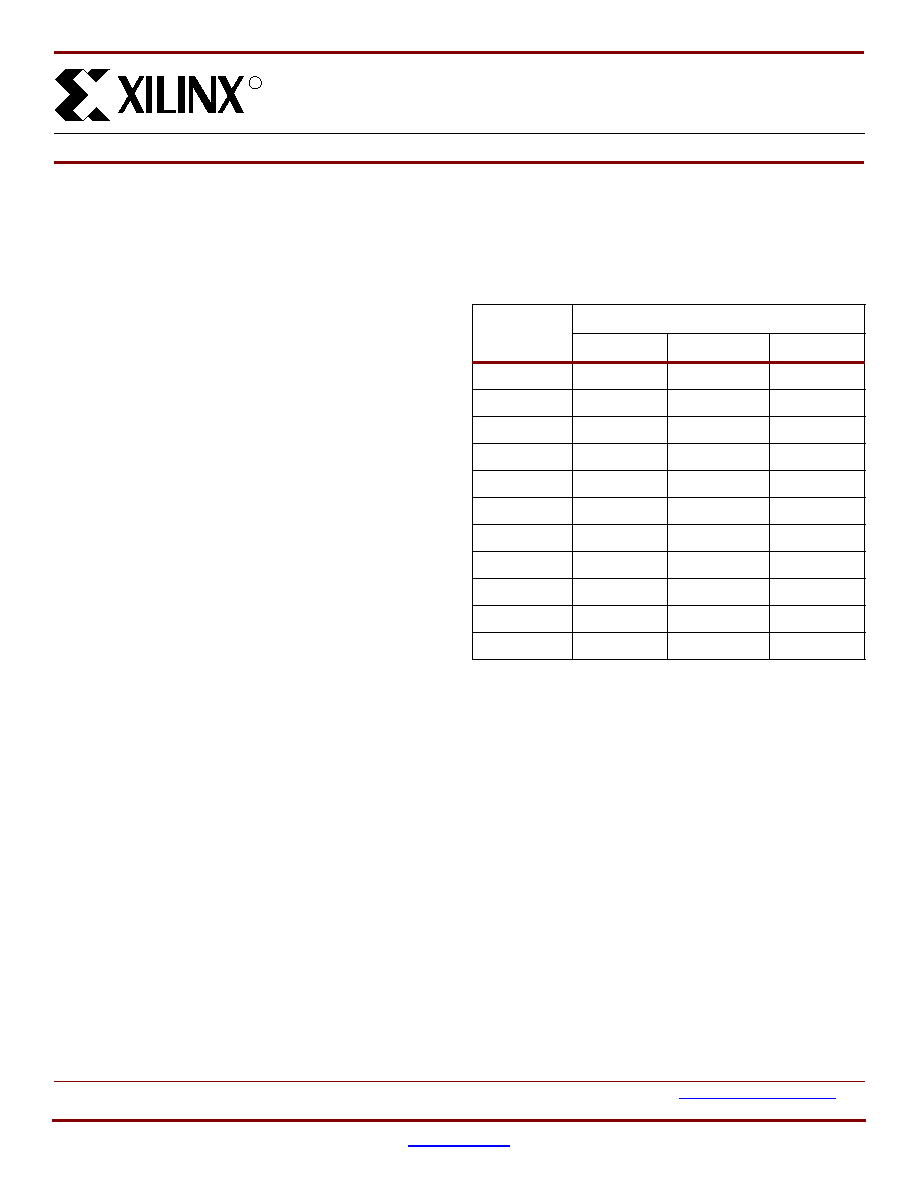
© 2000-2003 Xilinx, Inc. All rights reserved. All Xilinx trademarks, registered trademarks, patents, and disclaimers are as listed at
http://www.xilinx.com/legal.htm
.
All other trademarks and registered trademarks are the property of their respective owners. All specifications are subject to change without notice.
DS022-3 (v2.9.2) March 14, 2003
www.xilinx.com
Module 3 of 4
Production Product Specification
1-800-255-7778
1
Virtex-E Electrical Characteristics
Definition of Terms
Electrical and switching characteristics are specified on a
per-speed-grade basis and can be designated as Advance,
Preliminary, or Production. Each designation is defined as
follows:
Advance: These speed files are based on simulations only
and are typically available soon after device design specifi-
cations are frozen. Although speed grades with this desig-
nation are considered relatively stable and conservative,
some under-reporting might still occur.
Preliminary: These speed files are based on complete ES
(engineering sample) silicon characterization. Devices and
speed grades with this designation are intended to give a
better indication of the expected performance of production
silicon. The probability of under-reporting delays is greatly
reduced as compared to Advance data.
Production: These speed files are released once enough
production silicon of a particular device family member has
been characterized to provide full correlation between
speed files and devices over numerous production lots.
There is no under-reporting of delays, and customers
receive formal notification of any subsequent changes. Typ-
ically, the slowest speed grades transition to Production
before faster speed grades.
All specifications are representative of worst-case supply
voltage and junction temperature conditions. The parame-
ters included are common to popular designs and typical
applications. Contact the factory for design considerations
requiring more detailed information.
Table 1
correlates the current status of each Virtex-E device
with a corresponding speed file designation.
All specifications are subject to change without notice.
0
VirtexTM-E 1.8 V
Field Programmable Gate Arrays
DS022-3 (v2.9.2) March 14, 2003
0
0
Production Product Specification
R
Table 1: Virtex-E Device Speed Grade Designations
Device
Speed Grade Designations
Advance
Preliminary
Production
XCV50E
≠8, ≠7, ≠6
XCV100E
≠8, ≠7, ≠6
XCV200E
≠8, ≠7, ≠6
XCV300E
≠8, ≠7, ≠6
XCV400E
≠8, ≠7, ≠6
XCV600E
≠8, ≠7, ≠6
XCV1000E
≠8, ≠7, ≠6
XCV1600E
≠8, ≠7, ≠6
XCV2000E
≠8, ≠7, ≠6
XCV2600E
≠8, ≠7, ≠6
XCV3200E
≠8, ≠7, ≠6
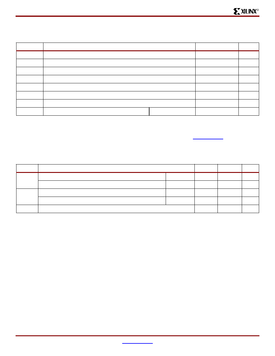
VirtexTM-E 1.8 V Field Programmable Gate Arrays
R
Module 3 of 4
www.xilinx.com
DS022-3 (v2.9.2) March 14, 2003
2
1-800-255-7778
Production Product Specification
DC Characteristics
Absolute Maximum Ratings
Recommended Operating Conditions
Symbol
Description
(1)
Units
V
CCINT
Internal Supply voltage relative to GND
≠0.5 to 2.0
V
V
CCO
Supply voltage relative to GND
≠0.5 to 4.0
V
V
REF
Input Reference Voltage
≠0.5 to 4.0
V
V
IN
(3)
Input voltage relative to GND
≠0.5 to V
CCO
+0.5
V
V
TS
Voltage applied to 3-state output
≠0.5 to 4.0
V
V
CC
Longest Supply Voltage Rise Time from 0 V - 1.71 V
50
ms
T
STG
Storage temperature (ambient)
≠65 to +150
∞C
T
J
Junction temperature
(2)
Plastic packages
+125
∞C
Notes:
1.
Stresses beyond those listed under Absolute Maximum Ratings can cause permanent damage to the device. These are stress
ratings only, and functional operation of the device at these or any other conditions beyond those listed under Operating Conditions
is not implied. Exposure to Absolute Maximum Ratings conditions for extended periods of time can affect device reliability.
2.
For soldering guidelines and thermal considerations, see the device packaging information on
www.xilinx.com
.
3.
Inputs configured as PCI are fully PCI compliant. This statement takes precedence over any specification that would imply that the
device is not PCI compliant.
Symbol
Description
Min
Max
Units
V
CCINT
Internal Supply voltage relative to GND, T
J
= 0
∞C to +85 ∞C
Commercial
1.8 ≠ 5%
1.8 + 5%
V
Internal Supply voltage relative to GND, T
J
= ≠40
∞C to +100 ∞C
Industrial
1.8 ≠ 5%
1.8 + 5%
V
V
CCO
Supply voltage relative to GND, T
J
= 0
∞C to +85 ∞C
Commercial
1.2
3.6
V
Supply voltage relative to GND, T
J
= ≠40
∞C to +100 ∞C
Industrial
1.2
3.6
V
T
IN
Input signal transition time
250
ns
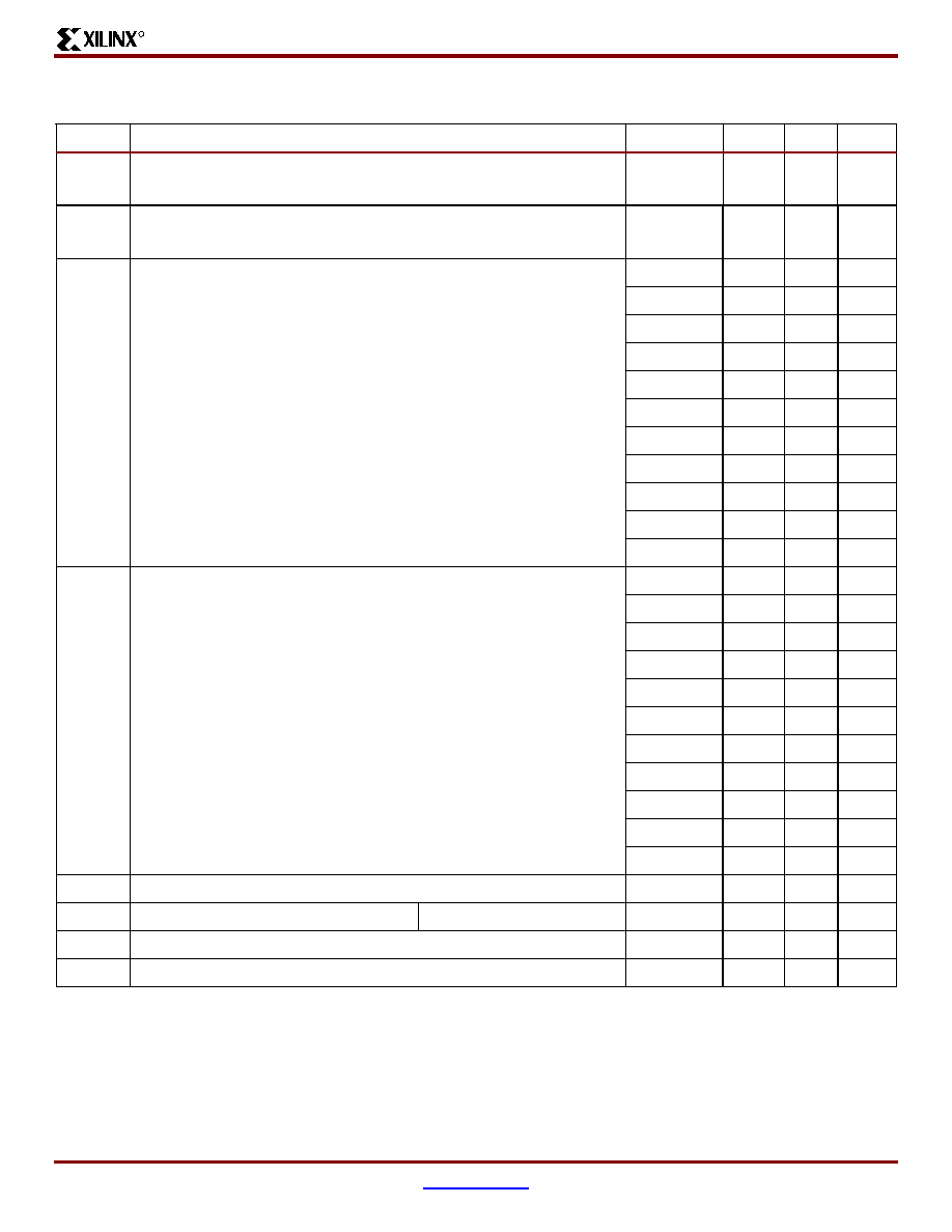
VirtexTM-E 1.8 V Field Programmable Gate Arrays
R
DS022-3 (v2.9.2) March 14, 2003
www.xilinx.com
Module 3 of 4
Production Product Specification
1-800-255-7778
3
DC Characteristics Over Recommended Operating Conditions
Symbol
Description
Device
Min
Max
Units
V
DRINT
Data Retention V
CCINT
Voltage
(below which configuration data might be lost)
All
1.5
V
V
DRIO
Data Retention V
CCO
Voltage
(below which configuration data might be lost)
All
1.2
V
I
CCINTQ
Quiescent V
CCINT
supply current (Note 1)
XCV50E
200
mA
XCV100E
200
mA
XCV200E
300
mA
XCV300E
300
mA
XCV400E
300
mA
XCV600E
400
mA
XCV1000E
500
mA
XCV1600E
500
mA
XCV2000E
500
mA
XCV2600E
500
mA
XCV3200E
500
mA
I
CCOQ
Quiescent V
CCO
supply current (Note 1)
XCV50E
2
mA
XCV100E
2
mA
XCV200E
2
mA
XCV300E
2
mA
XCV400E
2
mA
XCV600E
2
mA
XCV1000E
2
mA
XCV1600E
2
mA
XCV2000E
2
mA
XCV2600E
2
mA
XCV3200E
2
mA
I
L
Input or output leakage current
All
≠10
+10
µA
C
IN
Input capacitance (sample tested)
BGA, PQ, HQ, packages
All
8
pF
I
RPU
Pad pull-up (when selected) @ V
in
= 0 V, V
CCO
= 3.3 V (sample tested)
All
Note 2
0.25
mA
I
RPD
Pad pull-down (when selected) @ V
in
= 3.6 V (sample tested)
Note 2
0.25
mA
Notes:
1.
With no output current loads, no active input pull-up resistors, all I/O pins 3-stated and floating.
2.
Internal pull-up and pull-down resistors guarantee valid logic levels at unconnected input pins. These pull-up and pull-down resistors
do not guarantee valid logic levels when input pins are connected to other circuits.
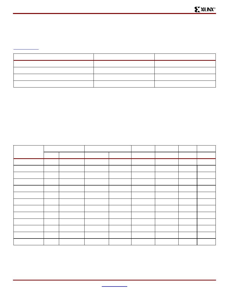
VirtexTM-E 1.8 V Field Programmable Gate Arrays
R
Module 3 of 4
www.xilinx.com
DS022-3 (v2.9.2) March 14, 2003
4
1-800-255-7778
Production Product Specification
Power-On Power Supply Requirements
Xilinx FPGAs require a certain amount of supply current during power-on to insure proper device operation. The actual
current consumed depends on the power-on ramp rate of the power supply. This is the time required to reach the nominal
power supply voltage of the device
1
from 0V. The fastest ramp rate is 0V to nominal voltage in 2 ms, and the slowest allowed
ramp rate is 0V to nominal voltage in 50 ms. For more details on power supply requirements, see XAPP158 on
www.xilinx.com
.
DC Input and Output Levels
Values for V
IL
and V
IH
are recommended input voltages. Values for I
OL
and I
OH
are guaranteed over the recommended
operating conditions at the V
OL
and V
OH
test points. Only selected standards are tested. These are chosen to ensure that
all standards meet their specifications. The selected standards are tested at minimum V
CCO
with the respective V
OL
and
V
OH
voltage levels shown. Other standards are sample tested.
Product (Commercial Grade)
Description
(2)
Current Requirement
(3)
XCV50E - XCV600E
Minimum required current supply
500 mA
XCV812E - XCV2000E
Minimum required current supply
1 A
XCV2600E - XCV3200E
Minimum required current supply
1.2 A
Virtex-E Family, Industrial Grade
Minimum required current supply
2 A
Notes:
1.
Ramp rate used for this specification is from 0 - 1.8 V DC. Peak current occurs on or near the internal power-on reset threshold and
lasts for less than 3 ms.
2.
Devices are guaranteed to initialize properly with the minimum current available from the power supply as noted above.
3.
Larger currents might result if ramp rates are forced to be faster.
Input/Output
Standard
V
IL
V
IH
V
OL
V
OH
I
OL
I
OH
V, Min
V, Max
V, Min
V, Max
V, Max
V, Min
mA
mA
LVTTL
(1)
≠ 0.5
0.8
2.0
3.6
0.4
2.4
24
≠ 24
LVCMOS2
≠ 0.5
0.7
1.7
2.7
0.4
1.9
12
≠ 12
LVCMOS18
≠ 0.5
35% V
CCO
65% V
CCO
1.95
0.4
V
CCO
≠ 0.4
8
≠ 8
PCI, 3.3 V
≠ 0.5
30% V
CCO
50% V
CCO
V
CCO
+ 0.5
10% V
CCO
90% V
CCO
Note 2
Note 2
GTL
≠ 0.5
V
REF
≠ 0.05
V
REF
+ 0.05
3.6
0.4
n/a
40
n/a
GTL+
≠ 0.5
V
REF
≠ 0.1
V
REF
+ 0.1
3.6
0.6
n/a
36
n/a
HSTL I
(3)
≠ 0.5
V
REF
≠ 0.1
V
REF
+ 0.1
3.6
0.4
V
CCO
≠ 0.4
8
≠8
HSTL III
≠ 0.5
V
REF
≠ 0.1
V
REF
+ 0.1
3.6
0.4
V
CCO
≠ 0.4
24
≠8
HSTL IV
≠ 0.5
V
REF
≠ 0.1
V
REF
+ 0.1
3.6
0.4
V
CCO
≠ 0.4
48
≠8
SSTL3 I
≠ 0.5
V
REF
≠ 0.2
V
REF
+ 0.2
3.6
V
REF
≠ 0.6
V
REF
+ 0.6
8
≠8
SSTL3 II
≠ 0.5
V
REF
≠ 0.2
V
REF
+ 0.2
3.6
V
REF
≠ 0.8
V
REF
+ 0.8
16
≠16
SSTL2 I
≠ 0.5
V
REF
≠ 0.2
V
REF
+ 0.2
3.6
V
REF
≠ 0.61
V
REF
+ 0.61
7.6
≠7.6
SSTL2 II
≠ 0.5
V
REF
≠ 0.2
V
REF
+ 0.2
3.6
V
REF
≠ 0.80
V
REF
+ 0.80
15.2
≠15.2
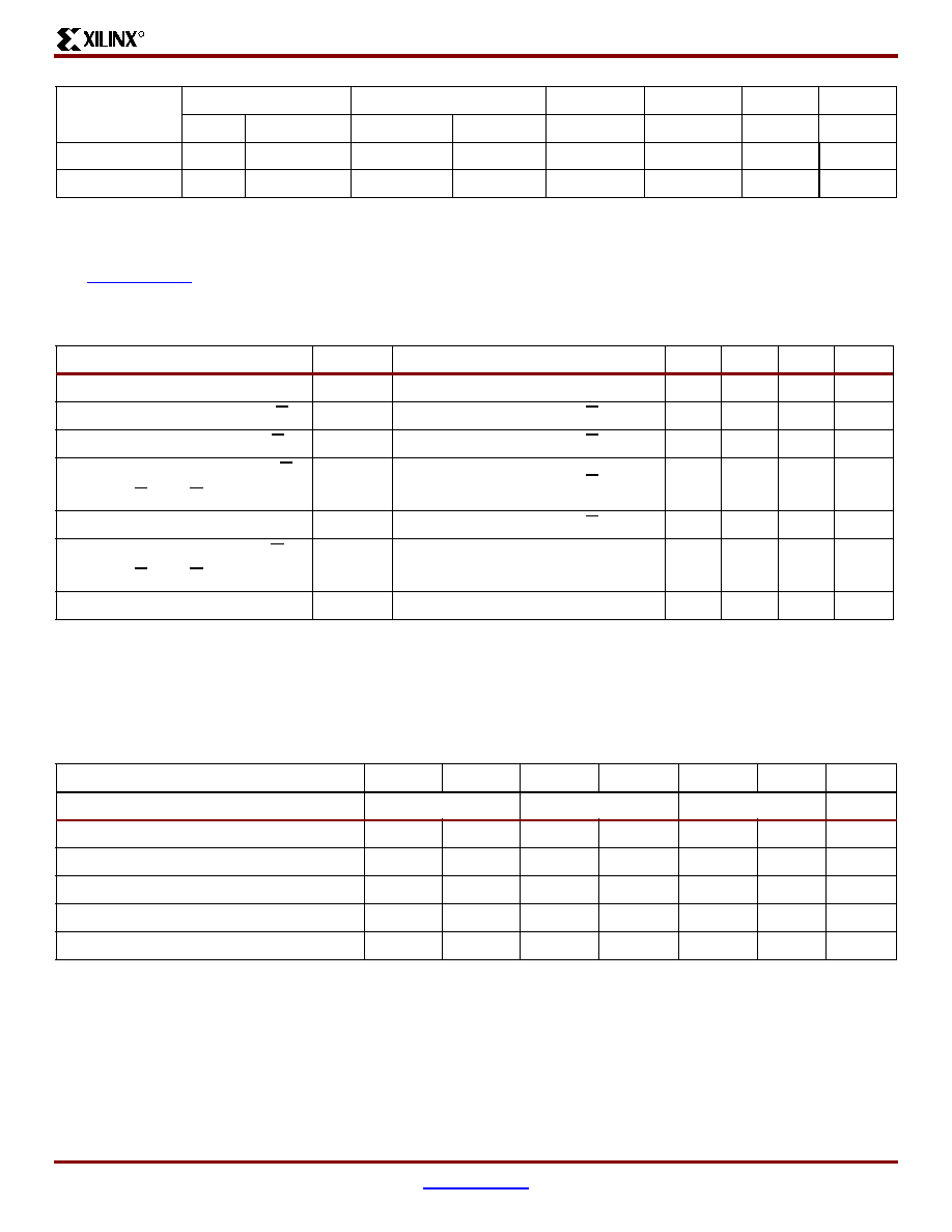
VirtexTM-E 1.8 V Field Programmable Gate Arrays
R
DS022-3 (v2.9.2) March 14, 2003
www.xilinx.com
Module 3 of 4
Production Product Specification
1-800-255-7778
5
LVDS DC Specifications
LVPECL DC Specifications
These values are valid at the output of the source termination pack shown under
LVPECL
, with a 100
differential load only.
The V
OH
levels are 200 mV below standard LVPECL levels and are compatible with devices tolerant of lower common-mode
ranges. The following table summarizes the DC output specifications of LVPECL.
CTT
≠ 0.5
V
REF
≠ 0.2
V
REF
+ 0.2
3.6
V
REF
≠ 0.4
V
REF
+ 0.4
8
≠8
AGP
≠ 0.5
V
REF
≠ 0.2
V
REF
+ 0.2
3.6
10% V
CCO
90% V
CCO
Note 2
Note 2
Notes:
1.
V
OL
and V
OH
for lower drive currents are sample tested.
2.
Tested according to the relevant specifications.
3.
DC input and output levels for HSTL18 (HSTL I/O standard with V
CCO
of 1.8 V) are provided in an HSTL white paper on
www.xilinx.com
.
DC Parameter
Symbol
Conditions
Min
Typ
Max
Units
Supply Voltage
V
CCO
2.375
2.5
2.625
V
Output High Voltage for Q and Q
V
OH
R
T
= 100
across Q and Q signals
1.25
1.425
1.6
V
Output Low Voltage for Q and Q
V
OL
R
T
= 100
across Q and Q signals
0.9
1.075
1.25
V
Differential Output Voltage (Q ≠ Q),
Q = High (Q ≠ Q), Q = High
V
ODIFF
R
T
= 100
across Q and Q signals
250
350
450
mV
Output Common-Mode Voltage
V
OCM
R
T
= 100
across Q and Q signals
1.125
1.25
1.375
V
Differential Input Voltage (Q ≠ Q),
Q = High (Q ≠ Q), Q = High
V
IDIFF
Common-mode input voltage = 1.25 V
100
350
NA
mV
Input Common-Mode Voltage
V
ICM
Differential input voltage =
±350 mV
0.2
1.25
2.2
V
Note: Refer to the Design Consideration section for termination schematics.
Input/Output
Standard
V
IL
V
IH
V
OL
V
OH
I
OL
I
OH
V, Min
V, Max
V, Min
V, Max
V, Max
V, Min
mA
mA
DC Parameter
Min
Max
Min
Max
Min
Max
Units
V
CCO
3.0
3.3
3.6
V
V
OH
1.8
2.11
1.92
2.28
2.13
2.41
V
V
OL
0.96
1.27
1.06
1.43
1.30
1.57
V
V
IH
1.49
2.72
1.49
2.72
1.49
2.72
V
V
IL
0.86
2.125
0.86
2.125
0.86
2.125
V
Differential Input Voltage
0.3
-
0.3
-
0.3
-
V
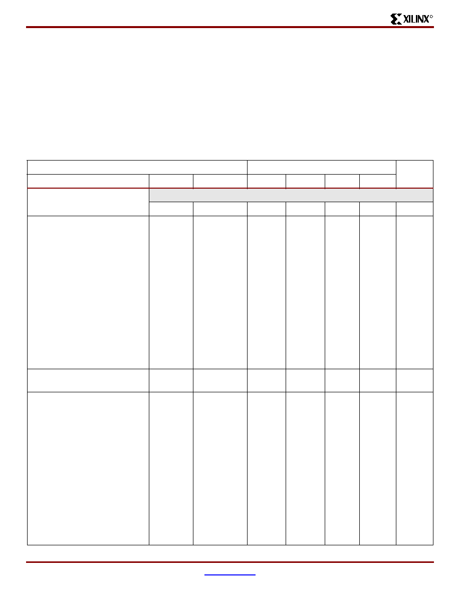
VirtexTM-E 1.8 V Field Programmable Gate Arrays
R
Module 3 of 4
www.xilinx.com
DS022-3 (v2.9.2) March 14, 2003
6
1-800-255-7778
Production Product Specification
Virtex-E Switching Characteristics
All devices are 100% functionally tested. Internal timing parameters are derived from measuring internal test patterns. Listed
below are representative values. For more specific, more precise, and worst-case guaranteed data, use the values reported
by the static timing analyzer (TRCE in the Xilinx Development System) and back-annotated to the simulation net list. All
timing parameters assume worst-case operating conditions (supply voltage and junction temperature). Values apply to all
Virtex-E devices unless otherwise noted.
IOB Input Switching Characteristics
Input delays associated with the pad are specified for LVTTL levels in
Table 2
. For other standards, adjust the delays with the
values shown in
IOB Input Switching Characteristics Standard Adjustments, page 8
.
Table 2: IOB Input Switching Characteristics
Speed Grade
(1)
Units
Description
(2)
Symbol
Device
Min
-8
-7
-6
Propagation Delays
Pad to I output, no delay
T
IOPI
All
0.43
0.8
0.8
0.8 ns,
max
Pad to I output, with delay
T
IOPID
XCV50E
0.51
1.0
1.0
1.0 ns,
max
XCV100E
0.51
1.0
1.0
1.0 ns,
max
XCV200E
0.51
1.0
1.0
1.0 ns,
max
XCV300E
0.51
1.0
1.0
1.0 ns,
max
XCV400E
0.51
1.0
1.0
1.0 ns,
max
XCV600E
0.51
1.0
1.0
1.0 ns,
max
XCV1000E
0.55
1.1
1.1
1.1 ns,
max
XCV1600E
0.55
1.1
1.1
1.1 ns,
max
XCV2000E
0.55
1.1
1.1
1.1 ns,
max
XCV2600E
0.55
1.1
1.1
1.1 ns,
max
XCV3200E
0.55
1.1
1.1
1.1 ns,
max
Pad to output IQ via transparent
latch, no delay
T
IOPLI
All
0.8
1.4
1.5
1.6 ns,
max
Pad to output IQ via transparent
latch, with delay
T
IOPLID
XCV50E
1.31
2.9
3.0
3.1 ns,
max
XCV100E
1.31
2.9
3.0
3.1 ns,
max
XCV200E
1.39
3.1
3.2
3.3 ns,
max
XCV300E
1.39
3.1
3.2
3.3 ns,
max
XCV400E
1.43
3.2
3.3
3.4 ns,
max
XCV600E
1.55
3.5
3.6
3.7 ns,
max
XCV1000E
1.55
3.5
3.6
3.7 ns,
max
XCV1600E
1.59
3.6
3.7
3.8 ns,
max
XCV2000E
1.59
3.6
3.7
3.8 ns,
max
XCV2600E
1.59
3.6
3.7
3.8 ns,
max
XCV3200E
1.59
3.6
3.7
3.8 ns,
max
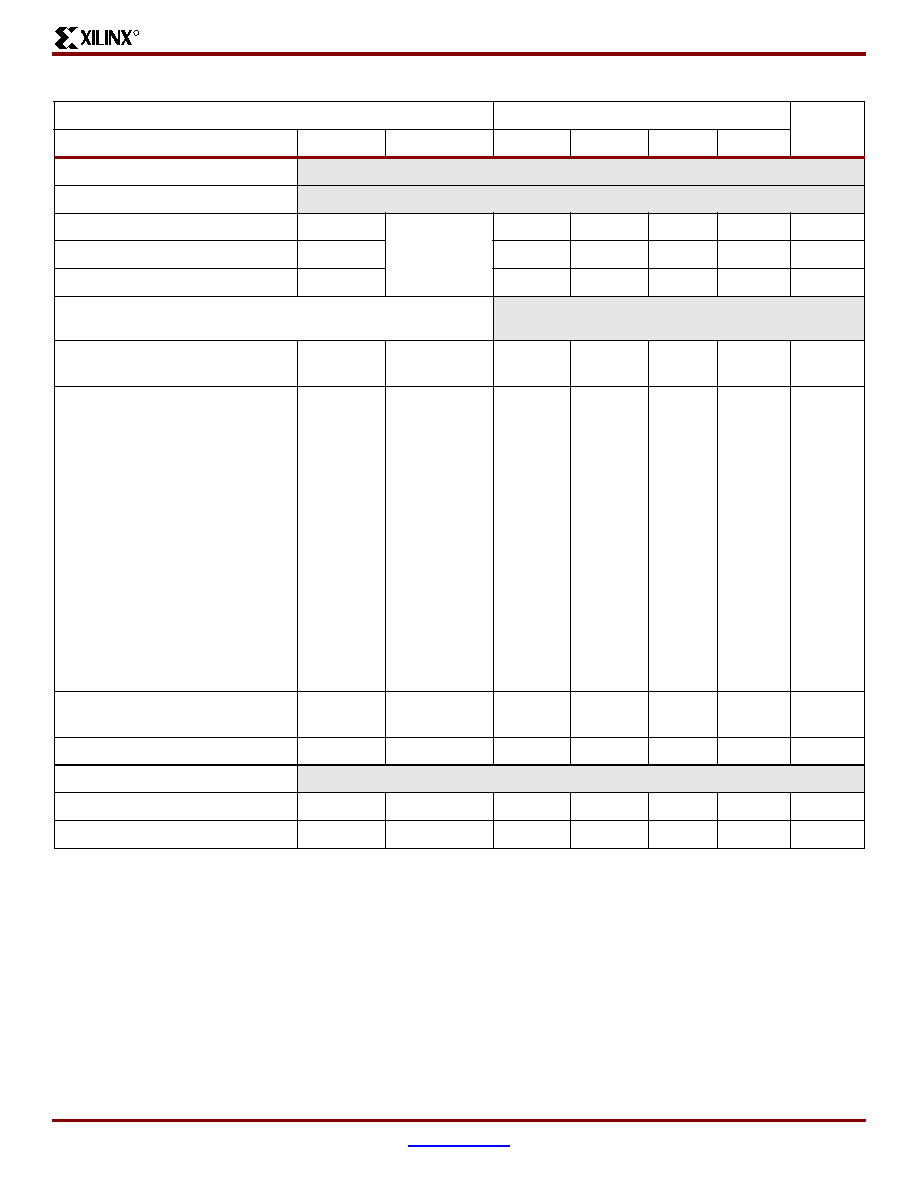
VirtexTM-E 1.8 V Field Programmable Gate Arrays
R
DS022-3 (v2.9.2) March 14, 2003
www.xilinx.com
Module 3 of 4
Production Product Specification
1-800-255-7778
7
Sequential Delays
Clock CLK
Minimum Pulse Width, High
T
CH
All
0.56
1.2
1.3
1.4
ns, min
Minimum Pulse Width, Low
T
CL
0.56
1.2
1.3
1.4
ns, min
Clock CLK to output IQ
T
IOCKIQ
0.18
0.4
0.7
0.7
ns, max
Setup and Hold Times with respect to Clock at IOB Input
Register
Pad, no delay
T
IOPICK
/
T
IOICKP
All
0.69 / 0
1.3 / 0
1.4 / 0
1.5 / 0
ns, min
Pad, with delay
T
IOPICKD
/
T
IOICKPD
XCV50E
1.25 / 0
2.8 / 0
2.9 / 0
2.9 / 0
ns, min
XCV100E
1.25 / 0
2.8 / 0
2.9 / 0
2.9 / 0
ns, min
XCV200E
1.33 / 0
3.0 / 0
3.1 / 0
3.1 / 0
ns, min
XCV300E
1.33 / 0
3.0 / 0
3.1 / 0
3.1 / 0
ns, min
XCV400E
1.37 / 0
3.1 / 0
3.2 / 0
3.2 / 0
ns, min
XCV600E
1.49 / 0
3.4 / 0
3.5 / 0
3.5 / 0
ns, min
XCV1000E
1.49 / 0
3.4 / 0
3.5 / 0
3.5 / 0
ns, min
XCV1600E
1.53 / 0
3.5 / 0
3.6 / 0
3.6 / 0
ns, min
XCV2000E
1.53 / 0
3.5 / 0
3.6 / 0
3.6 / 0
ns, min
XCV2600E
1.53 / 0
3.5 / 0
3.6 / 0
3.6 / 0
ns, min
XCV3200E
1.53 / 0
3.5 / 0
3.6 / 0
3.6 / 0
ns, min
ICE input
T
IOICECK
/
T
IOCKICE
All
0.28 /
0.0
0.55 /
0.01
0.7 /
0.01
0.7 /
0.01
ns, min
SR input (IFF, synchronous)
T
IOSRCKI
All
0.38
0.8
0.9
1.0 ns,
min
Set/Reset Delays
SR input to IQ (asynchronous)
T
IOSRIQ
All
0.54
1.1
1.2
1.4 ns,
max
GSR to output IQ
T
GSRQ
All
3.88
7.6
8.5
9.7 ns,
max
Notes:
1.
A Zero "0" Hold Time listing indicates no hold time or a negative hold time. Negative values can not be guaranteed "best-case", but
if a "0" is listed, there is no positive hold time.
2.
Input timing i for LVTTL is measured at 1.4 V. For other I/O standards, see
Table 4
.
Table 2: IOB Input Switching Characteristics (Continued)
Speed Grade
(1)
Units
Description
(2)
Symbol
Device
Min
-8
-7
-6

VirtexTM-E 1.8 V Field Programmable Gate Arrays
R
Module 3 of 4
www.xilinx.com
DS022-3 (v2.9.2) March 14, 2003
8
1-800-255-7778
Production Product Specification
IOB Input Switching Characteristics Standard Adjustments
Speed Grade
(1)
Units
Description
Symbol
Standard
Min
-8
-7
-6
Data Input Delay Adjustments
Standard-specific data input delay
adjustments
T
ILVTTL
LVTTL
0.0
0.0
0.0
0.0 ns
T
ILVCMOS2
LVCMOS2
≠0.02
0.0
0.0
0.0 ns
T
ILVCMOS18
LVCMOS18
0.12
+0.20
+0.20
+0.20
ns
T
ILVDS
LVDS
0.00
+0.15
+0.15
+0.15
ns
T
ILVPECL
LVPECL
0.00
+0.15
+0.15
+0.15
ns
T
IPCI33_3
PCI, 33 MHz, 3.3 V
≠0.05
+0.08
+0.08
+0.08
ns
T
IPCI66_3
PCI, 66 MHz, 3.3 V
≠0.05
≠0.11
≠0.11
≠0.11
ns
T
IGTL
GTL
+0.10
+0.14
+0.14
+0.14
ns
T
IGTLPLUS
GTL+
+0.06
+0.14
+0.14
+0.14
ns
T
IHSTL
HSTL
+0.02
+0.04
+0.04
+0.04
ns
T
ISSTL2
SSTL2
≠0.04
+0.04
+0.04
+0.04
ns
T
ISSTL3
SSTL3
≠0.02
+0.04
+0.04
+0.04
ns
T
ICTT
CTT
+0.01
+0.10
+0.10
+0.10
ns
T
IAGP
AGP
≠0.03
+0.04
+0.04
+0.04
ns
Notes:
1.
Input timing i for LVTTL is measured at 1.4 V. For other I/O standards, see
Table 4
.
Figure 1: Virtex-E Input/Output Block (IOB)
OBUFT
IBUF
Vref
ds022_02_091300
SR
CLK
ICE
OCE
O
I
IQ
T
TCE
D
CE
Q
SR
D
CE
Q
SR
D
CE
Q
SR
PAD
Programmable
Delay
Weak
Keeper

VirtexTM-E 1.8 V Field Programmable Gate Arrays
R
DS022-3 (v2.9.2) March 14, 2003
www.xilinx.com
Module 3 of 4
Production Product Specification
1-800-255-7778
9
IOB Output Switching Characteristics,
Figure 1
Output delays terminating at a pad are specified for LVTTL with 12 mA drive and fast slew rate. For other standards, adjust
the delays with the values shown in
IOB Output Switching Characteristics Standard Adjustments, page 10
.
Speed Grade
(1)
Units
Description
(2)
Symbol
Min
-8
-7
-6
Propagation Delays
O input to Pad
T
IOOP
1.04
2.5
2.7
2.9 ns,
max
O input to Pad via transparent latch
T
IOOLP
1.24
2.9
3.1
3.4 ns,
max
3-State Delays
T input to Pad high-impedance (Note 2)
T
IOTHZ
0.73
1.5
1.7
1.9 ns,
max
T input to valid data on Pad
T
IOTON
1.13
2.7
2.9
3.1 ns,
max
T input to Pad high-impedance via transparent
latch (Note 2)
T
IOTLPHZ
0.86
1.8
2.0
2.2 ns,
max
T input to valid data on Pad via transparent latch
T
IOTLPON
1.26
3.0
3.2
3.4 ns,
max
GTS to Pad high impedance (Note 2)
T
GTS
1.94
4.1
4.6
4.9 ns,
max
Sequential Delays
Clock CLK
Minimum Pulse Width, High
T
CH
0.56
1.2
1.3
1.4
ns, min
Minimum Pulse Width, Low
T
CL
0.56
1.2
1.3
1.4
ns, min
Clock CLK to Pad
T
IOCKP
0.97
2.4
2.8
2.9 ns,
max
Clock CLK to Pad high-impedance (synchronous)
(Note 2)
T
IOCKHZ
0.77
1.6
2.0
2.2 ns,
max
Clock CLK to valid data on Pad (synchronous)
T
IOCKON
1.17
2.8
3.2
3.4 ns,
max
Setup and Hold Times before/after Clock CLK
O input
T
IOOCK
/ T
IOCKO
0.43 / 0
0.9 / 0
1.0 / 0
1.1 / 0
ns, min
OCE input
T
IOOCECK
/ T
IOCKOCE
0.28 / 0
0.55 / 0.01
0.7 / 0
0.7 / 0
ns, min
SR input (OFF)
T
IOSRCKO
/ T
IOCKOSR
0.40 / 0
0.8 / 0
0.9 / 0
1.0 / 0
ns, min
3-State Setup Times, T input
T
IOTCK
/ T
IOCKT
0.26 / 0
0.51 / 0
0.6 / 0
0.7 / 0
ns, min
3-State Setup Times, TCE input
T
IOTCECK
/ T
IOCKTCE
0.30 / 0
0.6 / 0
0.7 / 0
0.8 / 0
ns, min
3-State Setup Times, SR input (TFF)
T
IOSRCKT
/ T
IOCKTSR
0.38 / 0
0.8 / 0
0.9 / 0
1.0 / 0
ns, min
Set/Reset Delays
SR input to Pad (asynchronous)
T
IOSRP
1.30
3.1
3.3
3.5 ns,
max
SR input to Pad high-impedance (asynchronous)
(Note 2)
T
IOSRHZ
1.08
2.2
2.4
2.7 ns,
max
SR input to valid data on Pad (asynchronous)
T
IOSRON
1.48
3.4
3.7
3.9 ns,
max
GSR to Pad
T
IOGSRQ
3.88
7.6
8.5
9.7 ns,
max
Notes:
1.
A Zero "0" Hold Time listing indicates no hold time or a negative hold time. Negative values can not be guaranteed "best-case", but
if a "0" is listed, there is no positive hold time.
2.
3-state turn-off delays should not be adjusted.

VirtexTM-E 1.8 V Field Programmable Gate Arrays
R
Module 3 of 4
www.xilinx.com
DS022-3 (v2.9.2) March 14, 2003
10
1-800-255-7778
Production Product Specification
IOB Output Switching Characteristics Standard Adjustments
Output delays terminating at a pad are specified for LVTTL with 12 mA drive and fast slew rate. For other standards, adjust
the delays by the values shown.
Speed Grade
Units
Description
Symbol
Standard
Min
-8
-7
-6
Output Delay Adjustments
Standard-specific adjustments for output
delays terminating at pads (based on
standard capacitive load, Csl)
T
OLVTTL_S2
LVTTL, Slow, 2 mA
4.2
+14.7
+14.7
+14.7
ns
T
OLVTTL_S4
4 mA
2.5
+7.5
+7.5
+7.5
ns
T
OLVTTL_S6
6 mA
1.8
+4.8
+4.8
+4.8
ns
T
OLVTTL_S8
8 mA
1.2
+3.0
+3.0
+3.0
ns
T
OLVTTL_S12
12 mA
1.0
+1.9
+1.9
+1.9
ns
T
OLVTTL_S16
16 mA
0.9
+1.7
+1.7
+1.7
ns
T
OLVTTL_S24
24 mA
0.8
+1.3
+1.3
+1.3
ns
T
OLVTTL_F2
LVTTL, Fast, 2 mA
1.9
+13.1
+13.1
+13.1
ns
T
OLVTTL_F4
4 mA
0.7
+5.3
+5.3
+5.3
ns
T
OLVTTL_F6
6 mA
0.20
+3.1
+3.1
+3.1
ns
T
OLVTTL_F8
8 mA
0.10
+1.0
+1.0
+1.0
ns
T
OLVTTL_F12
12 mA
0.0
0.0
0.0
0.0
ns
T
OLVTTL_F16
16 mA
≠0.10
≠0.05
≠0.05
≠0.05
ns
T
OLVTTL_F24
24 mA
≠0.10
≠0.20
≠0.20
≠0.20
ns
T
OLVCMOS_2
LVCMOS2
0.10
+0.09
+0.09
+0.09
ns
T
OLVCMOS_18
LVCMOS18
0.10
+0.7
+0.7
+0.7 ns
T
OLVDS
LVDS
≠0.39
≠1.2
≠1.2
≠1.2 ns
T
OLVPECL
LVPECL
≠0.20
≠0.41
≠0.41
≠0.41
ns
T
OPCI33_3
PCI, 33 MHz, 3.3 V
0.50
+2.3
+2.3
+2.3
ns
T
OPCI66_3
PCI, 66 MHz, 3.3 V
0.10
≠0.41
≠0.41
≠0.41
ns
T
OGTL
GTL
0.6
+0.49
+0.49
+0.49
ns
T
OGTLP
GTL+
0.7
+0.8
+0.8
+0.8 ns
T
OHSTL_I
HSTL I
0.10
≠0.51
≠0.51
≠0.51
ns
T
OHSTL_III
HSTL III
≠0.10
≠0.91
≠0.91
≠0.91
ns
T
OHSTL_IV
HSTL IV
≠0.20
≠1.01
≠1.01
≠1.01
ns
T
OSSTL2_I
SSTL2 I
≠0.10
≠0.51
≠0.51
≠0.51
ns
T
OSSTL2_II
SSTL2 II
≠0.20
≠0.91
≠0.91
≠0.91
ns
T
OSSTL3_I
SSTL3 I
≠0.20
≠0.51
≠0.51
≠0.51
ns
T
OSSTL3_II
SSTL3 II
≠0.30
≠1.01
≠1.01
≠1.01
ns
T
OCTT
CTT
0.0
≠0.61
≠0.61
≠0.61
ns
T
OAGP
AGP
≠0.1
≠0.91
≠0.91
≠0.91
ns
VirtexTM-E 1.8 V Field Programmable Gate Arrays
R
DS022-3 (v2.9.2) March 14, 2003
www.xilinx.com
Module 3 of 4
Production Product Specification
1-800-255-7778
11
Calculation of T
ioop
as a Function of Capacitance
T
ioop
is the propagation delay from the O Input of the IOB to
the pad. The values for T
ioop
are based on the standard
capacitive load (C
sl
) for each I/O standard as listed in
Table 3
.
For other capacitive loads, use the formulas below to calcu-
late the corresponding T
ioop
:
T
ioop
= T
ioop
+ T
opadjust
+
(C
load
≠ C
sl
) * fl
where:
T
opadjust
is reported above in the Output Delay
Adjustment section.
C
load
is the capacitive load for the design.
Table 3: Constants for Use in Calculation of T
ioop
Standard
Csl (pF)
fl (ns/pF)
LVTTL Fast Slew Rate, 2mA drive
35
0.41
LVTTL Fast Slew Rate, 4mA drive
35
0.20
LVTTL Fast Slew Rate, 6mA drive
35
0.13
LVTTL Fast Slew Rate, 8mA drive
35
0.079
LVTTL Fast Slew Rate, 12mA drive
35
0.044
LVTTL Fast Slew Rate, 16mA drive
35
0.043
LVTTL Fast Slew Rate, 24mA drive
35
0.033
LVTTL Slow Slew Rate, 2mA drive
35
0.41
LVTTL Slow Slew Rate, 4mA drive
35
0.20
LVTTL Slow Slew Rate, 6mA drive
35
0.10
LVTTL Slow Slew Rate, 8mA drive
35
0.086
LVTTL Slow Slew Rate, 12mA drive
35
0.058
LVTTL Slow Slew Rate, 16mA drive
35
0.050
LVTTL Slow Slew Rate, 24mA drive
35
0.048
LVCMOS2
35
0.041
LVCMOS18
35
0.050
PCI 33 MHZ 3.3 V
10
0.050
PCI 66 MHz 3.3 V
10
0.033
GTL
0
0.014
GTL+
0
0.017
HSTL Class I
20
0.022
HSTL Class III
20
0.016
HSTL Class IV
20
0.014
SSTL2 Class I
30
0.028
SSTL2 Class II
30
0.016
SSTL3 Class I
30
0.029
SSTL3 Class II
30
0.016
CTT
20
0.035
AGP
10
0.037
Notes:
1.
I/O parameter measurements are made with the capacitance
values shown above. See the application examples (in
Module 2 of this data sheet) for appropriate terminations.
2.
I/O standard measurements are reflected in the IBIS model
information except where the IBIS format precludes it.
Table 4: Delay Measurement Methodology
Standard
V
L
1
V
H
1
Meas.
Point
V
REF
(Typ)
2
LVTTL
0
3
1.4
-
LVCMOS2
0
2.5
1.125
-
PCI33_3
Per PCI Spec
-
PCI66_3
Per PCI Spec
-
GTL
V
REF
≠0.2
V
REF
+0.2
V
REF
0.80
GTL+
V
REF
≠
0.2
V
REF
+0.2
V
REF
1.0
HSTL Class I
V
REF
≠
0.5
V
REF
+0.5
V
REF
0.75
HSTL Class III
V
REF
≠
0.5
V
REF
+0.5
V
REF
0.90
HSTL Class IV
V
REF
≠
0.5
V
REF
+0.5
V
REF
0.90
SSTL3 I & II
V
REF
≠
1.0
V
REF
+1.0
V
REF
1.5
SSTL2 I & II
V
REF
≠
0.75
V
REF
+0.75
V
REF
1.25
CTT
V
REF
≠
0.2
V
REF
+0.2
V
REF
1.5
AGP
V
REF
≠
(0.2xV
CCO
)
V
REF
+
(0.2xV
CCO
)
V
REF
Per
AGP
Spec
LVDS
1.2
≠
0.125
1.2 + 0.125
1.2
LVPECL
1.6
≠
0.3
1.6 + 0.3
1.6
Notes:
1.
Input waveform switches between V
L
and V
H
.
2.
Measurements are made at V
REF
(Typ), Maximum, and
Minimum. Worst-case values are reported.
I/O parameter measurements are made with the
capacitance values shown in
Table 3
. See the application
examples (in Module 2 of this data sheet) for appropriate
terminations.
I/O standard measurements are reflected in the IBIS model
information except where the IBIS format precludes it.

VirtexTM-E 1.8 V Field Programmable Gate Arrays
R
Module 3 of 4
www.xilinx.com
DS022-3 (v2.9.2) March 14, 2003
12
1-800-255-7778
Production Product Specification
Clock Distribution Switching Characteristics
I/O Standard Global Clock Input Adjustments
Speed Grade
Units
Description
Symbol
Min
-8
-7
-6
GCLK IOB and Buffer
Global Clock PAD to output.
T
GPIO
0.38
0.7
0.7
0.7
ns, max
Global Clock Buffer I input to O output
T
GIO
0.11
0.20
0.45
0.50
ns, max
Description
Symbol
(1)
Standard
Speed Grade
Units
Min
-8
-7
-6
Data Input Delay Adjustments
Standard-specific global clock
input delay adjustments
T
GPLVTTL
LVTTL
0.0
0.0
0.0
0.0
ns, max
T
GPLVCMOS2
LVCMOS2
≠0.02
0.0
0.0
0.0
ns, max
T
GPLVCMOS18
LVCMOS18
0.12
0.20
0.20
0.20
ns, max
T
GLVDS
LVDS
0.23
0.38
0.38
0.38
ns, max
T
GLVPECL
LVPECL
0.23
0.38
0.38
0.38
ns, max
T
GPPCI33_3
PCI, 33 MHz, 3.3 V
≠0.05
0.08
0.08
0.08
ns, max
T
GPPCI66_3
PCI, 66 MHz, 3.3 V
≠0.05
≠0.11
≠0.11
≠0.11
ns, max
T
GPGTL
GTL
0.20
0.37
0.37
0.37
ns, max
T
GPGTLP
GTL+
0.20
0.37
0.37
0.37
ns, max
T
GPHSTL
HSTL
0.18
0.27
0.27
0.27
ns, max
T
GPSSTL2
SSTL2
0.21
0.27
0.27
0.27
ns, max
T
GPSSTL3
SSTL3
0.18
0.27
0.27
0.27
ns, max
T
GPCTT
CTT
0.22
0.33
0.33
0.33
ns, max
T
GPAGP
AGP
0.21
0.27
0.27
0.27
ns, max
Notes:
1.
Input timing for GPLVTTL is measured at 1.4 V. For other I/O standards, see
Table 4
.

VirtexTM-E 1.8 V Field Programmable Gate Arrays
R
DS022-3 (v2.9.2) March 14, 2003
www.xilinx.com
Module 3 of 4
Production Product Specification
1-800-255-7778
13
CLB Switching Characteristics
Delays originating at F/G inputs vary slightly according to the input used, see
Figure 2
. The values listed below are
worst-case. Precise values are provided by the timing analyzer.
Speed Grade
(1)
Units
Description
Symbol
Min
-8
-7
-6
Combinatorial Delays
4-input function: F/G inputs to X/Y outputs
T
ILO
0.19
0.40
0.42
0.47
ns, max
5-input function: F/G inputs to F5 output
T
IF5
0.36
0.76
0.8
0.9 ns,
max
5-input function: F/G inputs to X output
T
IF5X
0.35
0.74
0.8
0.9 ns,
max
6-input function: F/G inputs to Y output via F6 MUX
T
IF6Y
0.35
0.74
0.9
1.0 ns,
max
6-input function: F5IN input to Y output
T
F5INY
0.04
0.11
0.20
0.22
ns, max
Incremental delay routing through transparent latch to
XQ/YQ outputs
T
IFNCTL
0.27
0.63
0.7
0.8 ns,
max
BY input to YB output
T
BYYB
0.19
0.38
0.46
0.51
ns, max
Sequential Delays
FF Clock CLK to XQ/YQ outputs
T
CKO
0.34
0.78
0.9
1.0 ns,
max
Latch Clock CLK to XQ/YQ outputs
T
CKLO
0.40
0.77
0.9
1.0 ns,
max
Setup and Hold Times before/after Clock CLK
4-input function: F/G Inputs
T
ICK
/
T
CKI
0.39 / 0
0.9 / 0
1.0 / 0
1.1 / 0
ns, min
5-input function: F/G inputs
T
IF5CK
/
T
CKIF5
0.55 / 0
1.3 / 0
1.4 / 0
1.5 / 0
ns, min
6-input function: F5IN input
T
F5INCK
/
T
CKF5IN
0.27 / 0
0.6 / 0
0.8 / 0
0.8 / 0
ns, min
6-input function: F/G inputs via F6 MUX
T
IF6CK
/
T
CKIF6
0.58 / 0
1.3 / 0
1.5 / 0
1.6 / 0
ns, min
BX/BY inputs
T
DICK
/
T
CKDI
0.25 / 0
0.6 / 0
0.7 / 0
0.8 / 0
ns, min
CE input
T
CECK
/
T
CKCE
0.28 / 0
0.55 / 0
0.7 / 0
0.7 / 0
ns, min
SR/BY inputs (synchronous)
T
RCK /
T
CKR
0.24 / 0
0.46 / 0
0.52 / 0
0.6 / 0
ns, min
Clock CLK
Minimum Pulse Width, High
T
CH
0.56
1.2
1.3
1.4 ns,
min
Minimum Pulse Width, Low
T
CL
0.56
1.2
1.3
1.4 ns,
min
Set/Reset
Minimum Pulse Width, SR/BY inputs
T
RPW
0.94
1.9
2.1
2.4 ns,
min
Delay from SR/BY inputs to XQ/YQ outputs
(asynchronous)
T
RQ
0.39
0.8
0.9
1.0
ns, max
Toggle Frequency (MHz) (for export control)
F
TOG
-
416
400
357
MHz
Notes:
1.
A Zero "0" Hold Time listing indicates no hold time or a negative hold time. Negative values can not be guaranteed "best-case", but
if a "0" is listed, there is no positive hold time.
VirtexTM-E 1.8 V Field Programmable Gate Arrays
R
Module 3 of 4
www.xilinx.com
DS022-3 (v2.9.2) March 14, 2003
14
1-800-255-7778
Production Product Specification
Figure 2: Detailed View of Virtex-E Slice
BY
F5IN
SR
CLK
CE
BX
YB
Y
YQ
XB
X
XQ
G4
G3
G2
G1
F4
F3
F2
F1
CIN
0
1
1
0
F5
F5
ds022_05_092000
COUT
CY
D
CE
Q
D
CE
Q
F6
CK
WSO
WSH
WE
A4
BY DG
BX
DI
DI
O
WE
I3
I2
I1
I0
LUT
CY
I3
I2
I1
I0
O
DI
WE
LUT
INIT
INIT
REV
REV
VirtexTM-E 1.8 V Field Programmable Gate Arrays
R
DS022-3 (v2.9.2) March 14, 2003
www.xilinx.com
Module 3 of 4
Production Product Specification
1-800-255-7778
15
CLB Arithmetic Switching Characteristics
Setup times not listed explicitly can be approximated by decreasing the combinatorial delays by the setup time adjustment
listed. Precise values are provided by the timing analyzer.
Speed
Grade
(1)
Units
Description
Symbol
Min
-8
-7
-6
Combinatorial Delays
F operand inputs to X via XOR
T
OPX
0.32
0.68
0.8
0.8
ns, max
F operand input to XB output
T
OPXB
0.35
0.65
0.8
0.9
ns, max
F operand input to Y via XOR
T
OPY
0.59
1.07
1.4
1.5
ns, max
F operand input to YB output
T
OPYB
0.48
0.89
1.1
1.3
ns, max
F operand input to COUT output
T
OPCYF
0.37
0.71
0.9
1.0
ns, max
G operand inputs to Y via XOR
T
OPGY
0.34
0.72
0.8
0.9
ns, max
G operand input to YB output
T
OPGYB
0.47
0.78
1.2
1.3
ns, max
G operand input to COUT output
T
OPCYG
0.36
0.60
0.9
1.0
ns, max
BX initialization input to COUT
T
BXCY
0.19
0.36
0.51
0.57
ns, max
CIN input to X output via XOR
T
CINX
0.27
0.50
0.6
0.7
ns, max
CIN input to XB
T
CINXB
0.02
0.04
0.07
0.08
ns, max
CIN input to Y via XOR
T
CINY
0.26
0.45
0.7
0.7
ns, max
CIN input to YB
T
CINYB
0.16
0.28
0.38
0.43
ns, max
CIN input to COUT output
T
BYP
0.05
0.10
0.14
0.15
ns, max
Multiplier Operation
F1/2 operand inputs to XB output via AND
T
FANDXB
0.10
0.30
0.35
0.39
ns, max
F1/2 operand inputs to YB output via AND
T
FANDYB
0.28
0.56
0.7
0.8
ns, max
F1/2 operand inputs to COUT output via AND
T
FANDCY
0.17
0.38
0.46
0.51
ns, max
G1/2 operand inputs to YB output via AND
T
GANDYB
0.20
0.46
0.55
0.7
ns, max
G1/2 operand inputs to COUT output via AND
T
GANDCY
0.09
0.28
0.30
0.34
ns, max
Setup and Hold Times before/after Clock CLK
CIN input to FFX
T
CCKX
/T
CKCX
0.47 / 0
1.0 / 0
1.2 / 0
1.3 / 0
ns, min
CIN input to FFY
T
CCKY
/T
CKCY
0.49 / 0
0.92 / 0
1.2 / 0
1.3 / 0
ns, min
Notes:
1.
A Zero "0" Hold Time listing indicates no hold time or a negative hold time. Negative values can not be guaranteed "best-case", but
if a "0" is listed, there is no positive hold time.
VirtexTM-E 1.8 V Field Programmable Gate Arrays
R
Module 3 of 4
www.xilinx.com
DS022-3 (v2.9.2) March 14, 2003
16
1-800-255-7778
Production Product Specification
CLB Distributed RAM Switching Characteristics
Speed Grade
(1)
Units
Description
Symbol
Min
-8
-7
-6
Sequential Delays
Clock CLK to X/Y outputs (WE active) 16 x 1 mode
T
SHCKO16
0.67
1.38
1.5
1.7
ns, max
Clock CLK to X/Y outputs (WE active) 32 x 1 mode
T
SHCKO32
0.84
1.66
1.9
2.1
ns, max
Shift-Register Mode
Clock CLK to X/Y outputs
T
REG
1.25
2.39
2.9
3.2
ns, max
Setup and Hold Times before/after Clock CLK
F/G address inputs
T
AS
/T
AH
0.19 / 0
0.38 / 0
0.42 / 0
0.47 / 0
ns, min
BX/BY data inputs (DIN)
T
DS
/T
DH
0.44 / 0
0.87 / 0
0.97 / 0
1.09 / 0
ns, min
SR input (WE)
T
WS
/T
WH
0.29 / 0
0.57 / 0
0.7 / 0
0.8 / 0
ns, min
Clock CLK
Minimum Pulse Width, High
T
WPH
0.96
1.9
2.1
2.4 ns,
min
Minimum Pulse Width, Low
T
WPL
0.96
1.9
2.1
2.4 ns,
min
Minimum clock period to meet address write cycle time
T
WC
1.92
3.8
4.2
4.8 ns,
min
Shift-Register Mode
Minimum Pulse Width, High
T
SRPH
1.0
1.9
2.1
2.4 ns,
min
Minimum Pulse Width, Low
T
SRPL
1.0
1.9
2.1
2.4 ns,
min
Notes:
1.
A Zero "0" Hold Time listing indicates no hold time or a negative hold time. Negative values can not be guaranteed "best-case", but
if a "0" is listed, there is no positive hold time.
Figure 3: Dual-Port Block SelectRAM
WEB
ENB
RSTB
CLKB
ADDRB[#:0]
DIB[#:0]
WEA
ENA
RSTA
CLKA
ADDRA[#:0]
DIA[#:0]
DOA[#:0]
DOB[#:0]
RAMB4_S#_S#
ds022_06_121699
VirtexTM-E 1.8 V Field Programmable Gate Arrays
R
DS022-3 (v2.9.2) March 14, 2003
www.xilinx.com
Module 3 of 4
Production Product Specification
1-800-255-7778
17
Block RAM Switching Characteristics
TBUF Switching Characteristics
JTAG Test Access Port Switching Characteristics
Speed Grade
(1)
Units
Description
Symbol
Min
-8
-7
-6
Sequential Delays
Clock CLK to DOUT output
T
BCKO
0.63
2.46
3.1
3.5
ns, max
Setup and Hold Times before Clock CLK
ADDR inputs
T
BACK
/T
BCKA
0.42 / 0
0.9 / 0
1.0 / 0
1.1 / 0
ns, min
DIN inputs
T
BDCK
/T
BCKD
0.42 / 0
0.9 / 0
1.0 / 0
1.1 / 0
ns, min
EN input
T
BECK
/T
BCKE
0.97 / 0
2.0 / 0
2.2 / 0
2.5 / 0
ns, min
RST input
T
BRCK
/T
BCKR
0.9 / 0
1.8 / 0
2.1 / 0
2.3 / 0
ns, min
WEN input
T
BWCK
/T
BCKW
0.86 / 0
1.7 / 0
2.0 / 0
2.2 / 0
ns, min
Clock CLK
Minimum Pulse Width, High
T
BPWH
0.6
1.2
1.35
1.5 ns,
min
Minimum Pulse Width, Low
T
BPWL
0.6
1.2
1.35
1.5 ns,
min
CLKA -> CLKB setup time for different ports
T
BCCS
1.2
2.4
2.7
3.0
ns, min
Notes:
1.
A Zero "0" Hold Time listing indicates no hold time or a negative hold time. Negative values can not be guaranteed "best-case", but
if a "0" is listed, there is no positive hold time.
Speed Grade
Units
Description
Symbol
Min
-8
-7
-6
Combinatorial Delays
IN input to OUT output
T
IO
0.0
0.0
0.0
0 .0
ns, max
TRI input to OUT output high-impedance
T
OFF
0.05
0.092
0.10
0.11
ns, max
TRI input to valid data on OUT output
T
ON
0.05
0.092
0.10
0.11
ns, max
Description
Symbol
Value
Units
TMS and TDI Setup times before TCK
T
TAPTK
4.0
ns, min
TMS and TDI Hold times after TCK
T
TCKTAP
2.0
ns, min
Output delay from clock TCK to output TDO
T
TCKTDO
11.0
ns, max
Maximum TCK clock frequency
F
TCK
33
MHz, max
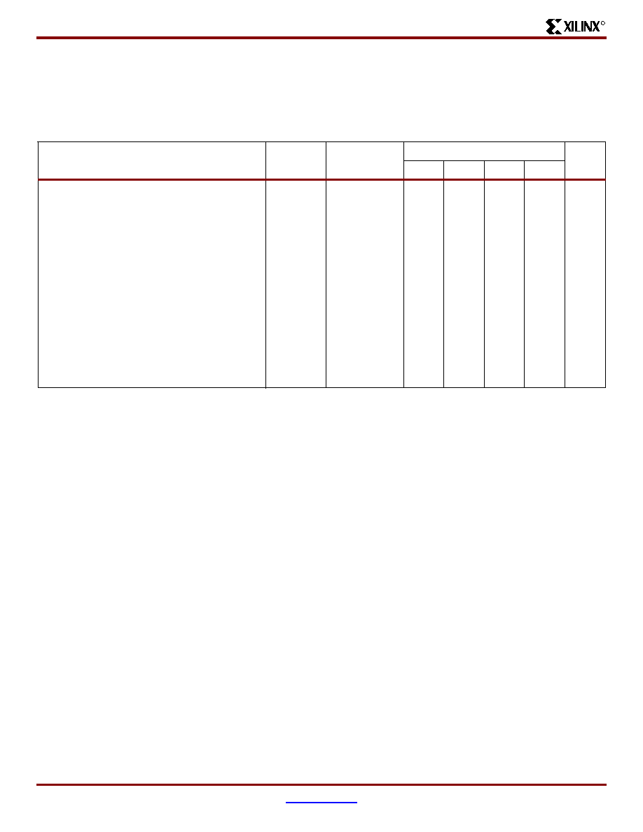
VirtexTM-E 1.8 V Field Programmable Gate Arrays
R
Module 3 of 4
www.xilinx.com
DS022-3 (v2.9.2) March 14, 2003
18
1-800-255-7778
Production Product Specification
Virtex-E Pin-to-Pin Output Parameter Guidelines
All devices are 100% functionally tested. Listed below are representative values for typical pin locations and normal clock
loading. Values are expressed in nanoseconds unless otherwise noted.
Global Clock Input to Output Delay for LVTTL, 12 mA, Fast Slew Rate, with DLL
Description
(1)
Symbol
Device
Speed Grade
(2, 3)
Units
Min
-8
-7
-6
LVTTL Global Clock Input to Output Delay using
Output Flip-flop, 12 mA, Fast Slew Rate, with
DLL. For data output with different standards,
adjust the delays with the values shown in
IOB
Output Switching Characteristics Standard
Adjustments, page 10
.
T
ICKOFDLL
XCV50E
1.0
3.1
3.1
3.1
ns
XCV100E
1.0
3.1
3.1
3.1
ns
XCV200E
1.0
3.1
3.1
3.1
ns
XCV300E
1.0
3.1
3.1
3.1
ns
XCV400E
1.0
3.1
3.1
3.1
ns
XCV600E
1.0
3.1
3.1
3.1
ns
XCV1000E
1.0
3.1
3.1
3.1
ns
XCV1600E
1.0
3.1
3.1
3.1
ns
XCV2000E
1.0
3.1
3.1
3.1
ns
XCV2600E
1.0
3.1
3.1
3.1
ns
XCV3200E
1.0
3.1
3.1
3.1
ns
Notes:
1.
Listed above are representative values where one global clock input drives one vertical clock line in each accessible column, and
where all accessible IOB and CLB flip-flops are clocked by the global clock net.
2.
Output timing is measured at 50% V
CC
threshold with 35 pF external capacitive load. For other I/O standards and different loads, see
Table 3
and
Table 4
.
3.
DLL output jitter is already included in the timing calculation.

VirtexTM-E 1.8 V Field Programmable Gate Arrays
R
DS022-3 (v2.9.2) March 14, 2003
www.xilinx.com
Module 3 of 4
Production Product Specification
1-800-255-7778
19
Global Clock Input to Output Delay for LVTTL, 12 mA, Fast Slew Rate, without DLL
Description
(1)
Symbol
Device
Speed Grade
(2)
Units
Min
-8
-7
-6
LVTTL Global Clock Input to Output Delay using
Output Flip-flop, 12 mA, Fast Slew Rate, without
DLL. For data output with different standards,
adjust the delays with the values shown in
IOB
Output Switching Characteristics Standard
Adjustments, page 10
.
T
ICKOF
XCV50E
1.5
4.2
4.4
4.6
ns
XCV100E
1.5
4.2
4.4
4.6
ns
XCV200E
1.5
4.3
4.5
4.7
ns
XCV300E
1.5
4.3
4.5
4.7
ns
XCV400E
1.5
4.4
4.6
4.8
ns
XCV600E
1.6
4.5
4.7
4.9
ns
XCV1000E
1.7
4.6
4.8
5.0
ns
XCV1600E
1.8
4.7
4.9
5.1
ns
XCV2000E
1.8
4.8
5.0
5.2
ns
XCV2600E
2.0
5.0
5.2
5.4
ns
XCV3200E
2.2
5.2
5.4
5.6
ns
Notes:
1.
Listed above are representative values where one global clock input drives one vertical clock line in each accessible column, and
where all accessible IOB and CLB flip-flops are clocked by the global clock net.
2.
Output timing is measured at 50% V
CC
threshold with 35 pF external capacitive load. For other I/O standards and different loads, see
Table 3
and
Table 4
.
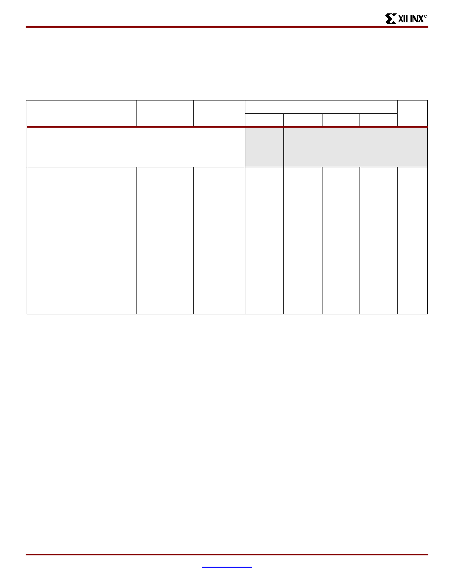
VirtexTM-E 1.8 V Field Programmable Gate Arrays
R
Module 3 of 4
www.xilinx.com
DS022-3 (v2.9.2) March 14, 2003
20
1-800-255-7778
Production Product Specification
Virtex-E Pin-to-Pin Input Parameter Guidelines
All devices are 100% functionally tested. Listed below are representative values for typical pin locations and normal clock
loading. Values are expressed in nanoseconds unless otherwise noted
Global Clock Set-Up and Hold for LVTTL Standard, with DLL
Description
(1)
Symbol
Device
Speed Grade
(2, 3)
Units
Min
-8
-7
-6
Input Setup and Hold Time Relative to Global Clock Input Signal
for LVTTL Standard. For data input with different standards,
adjust the setup time delay by the values shown in
IOB Input
Switching Characteristics Standard Adjustments, page 8
.
No Delay
T
PSDLL
/T
PHDLL
XCV50E
1.5 / ≠0.4
1.5 / ≠0.4
1.6 / ≠0.4
1.7 / ≠0.4
ns
Global Clock and IFF, with DLL
XCV100E
1.5 / ≠0.4
1.5 / ≠0.4
1.6 / ≠0.4
1.7 / ≠0.4
ns
XCV200E
1.5 / ≠0.4
1.5 / ≠0.4
1.6 / ≠0.4
1.7 / ≠0.4
ns
XCV300E
1.5 / ≠0.4
1.5 / ≠0.4
1.6 / ≠0.4
1.7 / ≠0.4
ns
XCV400E
1.5 / ≠0.4
1.5 / ≠0.4
1.6 / ≠0.4
1.7 / ≠0.4
ns
XCV600E
1.5 / ≠0.4
1.5 / ≠0.4
1.6 / ≠0.4
1.7 / ≠0.4
ns
XCV1000E
1.5 / ≠0.4
1.5 / ≠0.4
1.6 / ≠0.4
1.7 / ≠0.4
ns
XCV1600E
1.5 / ≠0.4
1.5 / ≠0.4
1.6 / ≠0.4
1.7 / ≠0.4
ns
XCV2000E
1.5 / ≠0.4
1.5 / ≠0.4
1.6 / ≠0.4
1.7 / ≠0.4
ns
XCV2600E
1.5 / ≠0.4
1.5 / ≠0.4
1.6 / ≠0.4
1.7 / ≠0.4
ns
XCV3200E
1.5 / ≠0.4
1.5 / ≠0.4
1.6 / ≠0.4
1.7 / ≠0.4
ns
Notes:
1.
IFF = Input Flip-Flop or Latch
2.
Setup time is measured relative to the Global Clock input signal with the fastest route and the lightest load. Hold time is measured
relative to the Global Clock input signal with the slowest route and heaviest load.
3.
DLL output jitter is already included in the timing calculation.
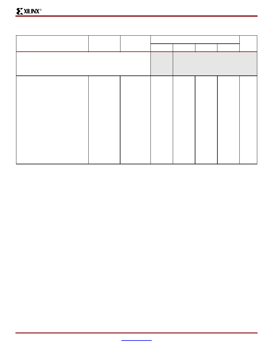
VirtexTM-E 1.8 V Field Programmable Gate Arrays
R
DS022-3 (v2.9.2) March 14, 2003
www.xilinx.com
Module 3 of 4
Production Product Specification
1-800-255-7778
21
Global Clock Set-Up and Hold for LVTTL Standard, without DLL
Description
(1)
Symbol
Device
Speed Grade
(2, 3)
Units
Min
-8
-7
-6
Input Setup and Hold Time Relative to Global Clock Input Signal
for LVTTL Standard. For data input with different standards, adjust
the setup time delay by the values shown in
IOB Input Switching
Characteristics Standard Adjustments, page 8
.
Full Delay
T
PSFD
/T
PHFD
XCV50E
1.8 / 0
1.8 / 0
1.8 / 0
1.8 / 0
ns
Global Clock and IFF, without DLL
XCV100E
1.8 / 0
1.8 / 0
1.8 / 0
1.8 / 0
ns
XCV200E
1.9 / 0
1.9 / 0
1.9 / 0
1.9 / 0
ns
XCV300E
2.0 / 0
2.0 / 0
2.0 / 0
2.0 / 0
ns
XCV400E
2.0 / 0
2.0 / 0
2.0 / 0
2.0 / 0
ns
XCV600E
2.1 / 0
2.1 / 0
2.1 / 0
2.1 / 0
ns
XCV1000E
2.3 / 0
2.3 / 0
2.3 / 0
2.3 / 0
ns
XCV1600E
2.5 / 0
2.5 / 0
2.5 / 0
2.5 / 0
ns
XCV2000E
2.5 / 0
2.5 / 0
2.5 / 0
2.5 / 0
ns
XCV2600E
2.7 / 0
2.7 / 0
2.7 / 0
2.7 / 0
ns
XCV3200E
2.8 / 0
2.8 / 0
2.8 / 0
2.8 / 0
ns
Notes:
1.
IFF = Input Flip-Flop or Latch
2.
Setup time is measured relative to the Global Clock input signal with the fastest route and the lightest load. Hold time is measured
relative to the Global Clock input signal with the slowest route and heaviest load.
3.
A Zero "0" Hold Time listing indicates no hold time or a negative hold time. Negative values can not be guaranteed "best-case", but
if a "0" is listed, there is no positive hold time.
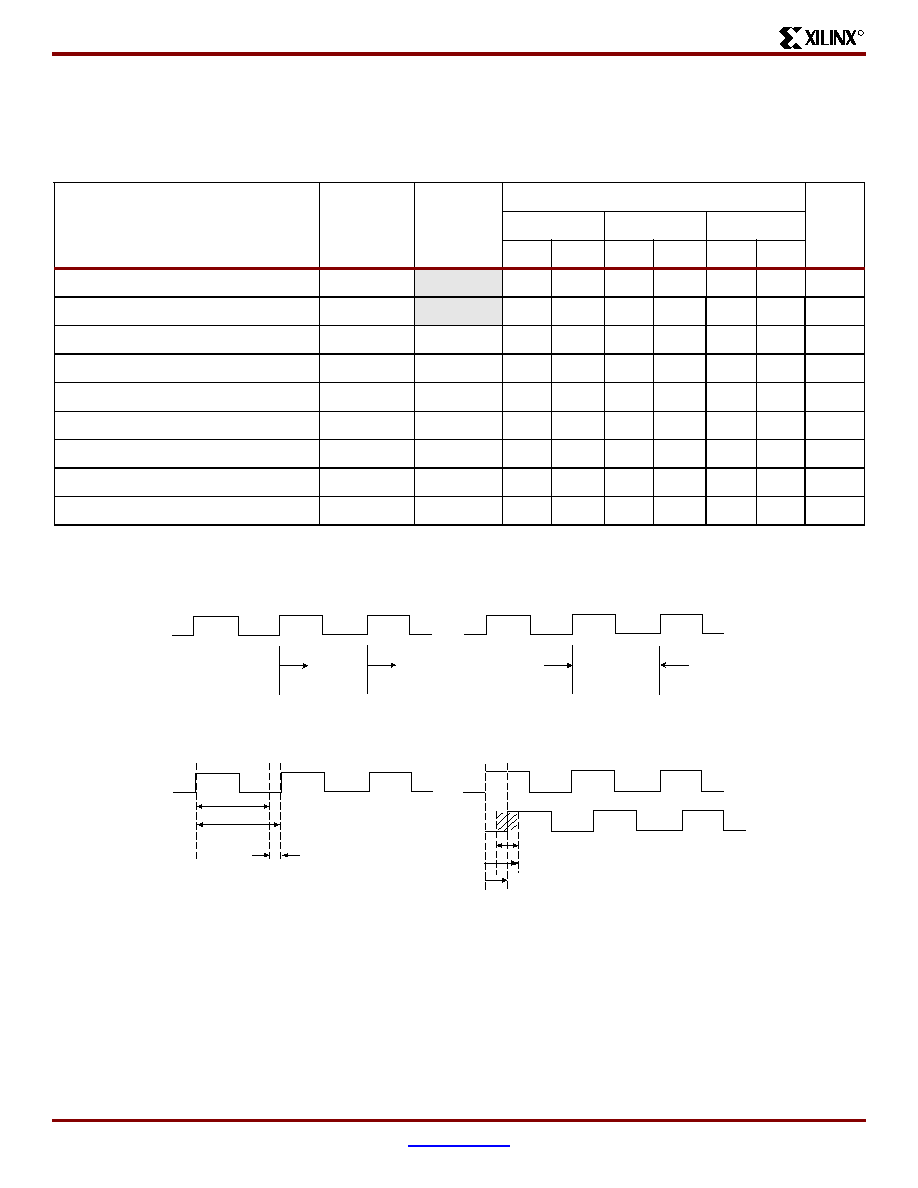
VirtexTM-E 1.8 V Field Programmable Gate Arrays
R
Module 3 of 4
www.xilinx.com
DS022-3 (v2.9.2) March 14, 2003
22
1-800-255-7778
Production Product Specification
DLL Timing Parameters
All devices are 100 percent functionally tested. Because of the difficulty in directly measuring many internal timing
parameters, those parameters are derived from benchmark timing patterns. The following guidelines reflect worst-case
values across the recommended operating conditions.
Description
Symbol
F
CLKIN
Speed Grade
Units
-8
-7
-6
Min
Max
Min
Max
Min
Max
Input Clock Frequency (CLKDLLHF)
FCLKINHF
60
350
60
320
60
275
MHz
Input Clock Frequency (CLKDLL)
FCLKINLF
25
160
25
160
25
135
MHz
Input Clock Low/High Pulse Width
T
DLLPW
25 MHz
5.0
5.0
5.0
ns
50 MHz
3.0
3.0
3.0
ns
100 MHz
2.4
2.4
2.4
ns
150 MHz
2.0
2.0
2.0
ns
200 MHz
1.8
1.8
1.8
ns
250 MHz
1.5
1.5
1.5
ns
300 MHz
1.3
1.3
NA
ns
Figure 4: DLL Timing Waveforms
TCLKIN
TCLKIN + TIPTOL
Period Tolerance: the allowed input clock period change in nanoseconds.
Output Jitter: the difference between an ideal
reference clock edge and the actual design.
_
ds022_24_091200
Ideal Period
Actual Period
+ Jitter
+/- Jitter
+ Maximum
Phase Difference
Phase Offset and Maximum Phase Difference
+ Phase Offset

VirtexTM-E 1.8 V Field Programmable Gate Arrays
R
DS022-3 (v2.9.2) March 14, 2003
www.xilinx.com
Module 3 of 4
Production Product Specification
1-800-255-7778
23
DLL Clock Tolerance, Jitter, and Phase Information
All DLL output jitter and phase specifications determined through statistical measurement at the package pins using a clock
mirror configuration and matched drivers.
CLKDLLHF
CLKDLL
Units
Description
Symbol
F
CLKIN
Min
Max
Min
Max
Input Clock Period Tolerance
T
IPTOL
-
1.0
-
1.0
ns
Input Clock Jitter Tolerance (Cycle to Cycle)
T
IJITCC
-
± 150
-
± 300
ps
Time Required for DLL to Acquire Lock
(6)
T
LOCK
> 60 MHz
-
20
-
20
µs
50 - 60 MHz
-
-
-
25
µs
40 - 50 MHz
-
-
-
50
µs
30 - 40 MHz
-
-
-
90
µs
25 - 30 MHz
-
-
-
120
µs
Output Jitter (cycle-to-cycle) for any DLL Clock Output
(1)
T
OJITCC
± 60
± 60
ps
Phase Offset between CLKIN and CLKO
(2)
T
PHIO
± 100
± 100
ps
Phase Offset between Clock Outputs on the DLL
(3)
T
PHOO
± 140
± 140
ps
Maximum Phase Difference between CLKIN and CLKO
(4)
T
PHIOM
± 160
± 160
ps
Maximum Phase Difference between Clock Outputs on the DLL
(5)
T
PHOOM
± 200
± 200
ps
Notes:
1.
Output Jitter is cycle-to-cycle jitter measured on the DLL output clock and is based on a maximum tap delay resolution, excluding
input clock jitter.
2.
Phase Offset between CLKIN and CLKO is the worst-case fixed time difference between rising edges of CLKIN and CLKO,
excluding Output Jitter and input clock jitter.
3.
Phase Offset between Clock Outputs on the DLL is the worst-case fixed time difference between rising edges of any two DLL
outputs, excluding Output Jitter and input clock jitter.
4.
Maximum Phase Difference between CLKIN an CLKO is the sum of Output Jitter and Phase Offset between CLKIN and CLKO,
or the greatest difference between CLKIN and CLKO rising edges due to DLL alone (excluding input clock jitter).
5.
Maximum Phase DIfference between Clock Outputs on the DLL is the sum of Output JItter and Phase Offset between any DLL
clock outputs, or the greatest difference between any two DLL output rising edges sue to DLL alone (excluding input clock jitter).
6.
Add 30% to the value for industrial grade parts.

VirtexTM-E 1.8 V Field Programmable Gate Arrays
R
Module 3 of 4
www.xilinx.com
DS022-3 (v2.9.2) March 14, 2003
24
1-800-255-7778
Production Product Specification
Revision History
The following table shows the revision history for this document.
Date
Version
Revision
12/7/99
1.0
Initial Xilinx release.
1/10/00
1.1
Re-released with spd.txt v. 1.18, FG860/900/1156 package information, and additional DLL,
Select RAM and SelectI/O information.
1/28/00
1.2
Added Delay Measurement Methodology table, updated SelectI/O section, Figures 30, 54,
& 55, text explaining Table 5, T
BYP
values, buffered Hex Line info, p. 8, I/O Timing
Measurement notes, notes for Tables 15, 16, and corrected F1156 pinout table footnote
references.
2/29/00
1.3
Updated pinout tables, V
CC
page 20, and corrected Figure 20.
5/23/00
1.4
Correction to table on p. 22.
7/10/00
1.5
∑
Numerous minor edits.
∑
Data sheet upgraded to Preliminary.
∑
Preview -8 numbers added to Virtex-E Electrical Characteristics tables.
8/1/00
1.6
∑
Reformatted entire document to follow new style guidelines.
∑
Changed speed grade values in tables on pages 35-37.
9/20/00
1.7
∑
Min values added to Virtex-E Electrical Characteristics tables.
∑
XCV2600E and XCV3200E numbers added to Virtex-E Electrical Characteristics
tables (Module 3).
∑
Corrected user I/O count for XCV100E device in Table 1 (Module 1).
∑
Changed several pins to "No Connect in the XCV100E" and removed duplicate V
CCINT
pins in Table ~ (Module 4).
∑
Changed pin J10 to "No connect in XCV600E" in Table 74 (Module 4).
∑
Changed pin J30 to "VREF option only in the XCV600E" in Table 74 (Module 4).
∑
Corrected pair 18 in Table 75 (Module 4) to be "AO in the XCV1000E, XCV1600E".
11/20/00
1.8
∑
Upgraded speed grade -8 numbers in Virtex-E Electrical Characteristics tables to
Preliminary.
∑
Updated minimums in Table 13 and added notes to Table 14.
∑
Added to note 2 to Absolute Maximum Ratings.
∑
Changed speed grade -8 numbers for T
SHCKO32
, T
REG
, T
BCCS
, and T
ICKOF
.
∑
Changed all minimum hold times to ≠0.4 under Global Clock Set-Up and Hold for
LVTTL Standard, with DLL.
∑
Revised maximum T
DLLPW
in -6 speed grade for DLL Timing Parameters.
∑
Changed GCLK0 to BA22 for FG860 package in Table 46.
2/12/01
1.9
∑
Revised footnote for Table 14.
∑
Added numbers to Virtex-E Electrical Characteristics tables for XCV1000E and
XCV2000E devices.
∑
Updated Table 27 and Table 78 to include values for XCV400E and XCV600E devices.
∑
Revised Table 62 to include pinout information for the XCV400E and XCV600E devices
in the BG560 package.
∑
Updated footnotes 1 and 2 for Table 76 to include XCV2600E and XCV3200E devices.
4/02/01
2.0
∑
Updated numerous values in
Virtex-E Switching Characteristics
tables.
∑
Converted data sheet to modularized format. See the
Virtex-E Data Sheet
section.
4/19/01
2.1
∑
Updated values in
Virtex-E Switching Characteristics
tables.
VirtexTM-E 1.8 V Field Programmable Gate Arrays
R
DS022-3 (v2.9.2) March 14, 2003
www.xilinx.com
Module 3 of 4
Production Product Specification
1-800-255-7778
25
Virtex-E Data Sheet
The Virtex-E Data Sheet contains the following modules:
∑
DS022-1, Virtex-E 1.8V FPGAs:
Introduction and Ordering Information (Module 1)
∑
DS022-2, Virtex-E 1.8V FPGAs:
Functional Description (Module 2)
∑
DS022-3, Virtex-E 1.8V FPGAs:
DC and Switching Characteristics (Module 3)
∑
DS022-4, Virtex-E 1.8V FPGAs:
Pinout Tables (Module 4)
07/23/01
2.2
∑
Under
Absolute Maximum Ratings
, changed (T
SOL
) to 220
∞C.
∑
Changes made to SSTL symbol names in
IOB Input Switching Characteristics
Standard Adjustments
table.
07/26/01
2.3
∑
Removed T
SOL
parameter and added footnote to
Absolute Maximum Ratings
table.
9/18/01
2.4
∑
Reworded power supplies footnote to
Absolute Maximum Ratings
table.
10/25/01
2.5
∑
Updated the speed grade designations used in data sheets, and added
Table 1
, which
shows the current speed grade designation for each device.
∑
Added XCV2600E and XCV3200E values to
DC Characteristics Over Recommended
Operating Conditions
and
Power-On Power Supply Requirements
tables.
11/09/01
2.6
∑
Updated the
Power-On Power Supply Requirements
table.
02/01/02
2.7
∑
Updated footnotes to the
DC Input and Output Levels
and
DLL Clock Tolerance,
Jitter, and Phase Information
tables.
07/17/02
2.8
∑
Data sheet designation upgraded from Preliminary to Production.
∑
Removed mention of MIL-M-38510/605 specification.
∑
Added link to XAPP158 from the
Power-On Power Supply Requirements
section.
09/10/02
2.9
∑
Revised V
IN
in
Absolute Maximum Ratings
table.
∑
Added Clock CLK switching characteristics to
Table 2, "IOB Input Switching
Characteristics," on page 6
and
IOB Output Switching Characteristics, Figure 1
.
12/22/02
2.9.1
∑
Added footnote regarding V
IN
PCI compliance to
Absolute Maximum Ratings
table.
∑
The fastest ramp rate is 0V to nominal voltage in 2 ms
03/14/03
2.9.2
∑
Under
Power-On Power Supply Requirements
, the fastest ramp rate is no longer a
"suggested" rate.
Date
Version
Revision

VirtexTM-E 1.8 V Field Programmable Gate Arrays
R
Module 3 of 4
www.xilinx.com
DS022-3 (v2.9.2) March 14, 2003
26
1-800-255-7778
Production Product Specification

© 2000-2003 Xilinx, Inc. All rights reserved. All Xilinx trademarks, registered trademarks, patents, and disclaimers are as listed at
http://www.xilinx.com/legal.htm
.
All other trademarks and registered trademarks are the property of their respective owners. All specifications are subject to change without notice.
DS022-4 (v2.5) March 14, 2003
www.xilinx.com
Module 4 of 4
Production Product Specification
1-800-255-7778
1
Virtex-E Pin Definitions
0
VirtexTM-E 1.8 V
Field Programmable Gate Arrays
DS022-4 (v2.5) March 14, 2003
0
0
Production Product Specification
R
Pin Name
Dedicated Pin
Direction
Description
GCK0, GCK1,
GCK2, GCK3
Yes
Input
Clock input pins that connect to Global Clock Buffers.
M0, M1, M2
Yes
Input
Mode pins are used to specify the configuration mode.
CCLK
Yes
Input or
Output
The configuration Clock I/O pin: it is an input for SelectMAP and
slave-serial modes, and output in master-serial mode. After
configuration, it is input only, logic level = Don't Care.
PROGRAM
Yes
Input
Initiates a configuration sequence when asserted Low.
DONE
Yes
Bidirectional
Indicates that configuration loading is complete, and that the start-up
sequence is in progress. The output can be open drain.
INIT
No
Bidirectional
(Open-drain)
When Low, indicates that the configuration memory is being cleared.
The pin becomes a user I/O after configuration.
BUSY/DOUT
No
Output
In SelectMAP mode, BUSY controls the rate at which configuration
data is loaded. The pin becomes a user I/O after configuration unless
the SelectMAP port is retained.
In bit-serial modes, DOUT provides preamble and configuration data
to downstream devices in a daisy-chain. The pin becomes a user I/O
after configuration.
D0/DIN,
D1, D2,
D3, D4,
D5, D6,
D7
No
Input or
Output
In SelectMAP mode, D0-7 are configuration data pins. These pins
become user I/Os after configuration unless the SelectMAP port is
retained.
In bit-serial modes, DIN is the single data input. This pin becomes a
user I/O after configuration.
WRITE
No
Input
In SelectMAP mode, the active-low Write Enable signal. The pin
becomes a user I/O after configuration unless the SelectMAP port is
retained.
CS
No
Input
In SelectMAP mode, the active-low Chip Select signal. The pin
becomes a user I/O after configuration unless the SelectMAP port is
retained.
TDI, TDO,
TMS, TCK
Yes
Mixed
Boundary-scan Test-Access-Port pins, as defined in IEEE1149.1.
DXN, DXP
Yes
N/A
Temperature-sensing diode pins. (Anode: DXP, cathode: DXN)
V
CCINT
Yes
Input
Power-supply pins for the internal core logic.
V
CCO
Yes
Input
Power-supply pins for the output drivers (subject to banking rules)
V
REF
No
Input
Input threshold voltage pins. Become user I/Os when an external
threshold voltage is not needed (subject to banking rules).
GND
Yes
Input
Ground

VirtexTM-E 1.8 V Field Programmable Gate Arrays
R
Module 4 of 4
www.xilinx.com
DS022-4 (v2.5) March 14, 2003
2
1-800-255-7778
Production Product Specification
Pinout Differences Between Virtex and Virtex-E Families
The same device in the same package for the Virtex-E and
Virtex families are pin-compatible with some minor excep-
tions, listed in
Table 1
.
XCV200E Device, FG456 Package
The Virtex-E XCV200E has two I/O pins swapped with the
Virtex XCV200 to accommodate differential clock pairing.
XCV400E Device, FG676 Package
The Virtex-E XCV400E has two I/O pins swapped with the
Virtex XCV400 to accommodate differential clock pairing.
All Devices, PQ240 and HQ240 Packages
The Virtex devices in PQ240 and HQ240 packages do not
have V
CCO
banking, but Virtex-E devices do. To achieve
this, eight Virtex I/O pins (P232, P207, P176, P146, P116,
P85, P55, and P25) are now VCCO pins in the Virtex-E fam-
ily. This change also requires one Virtex I/O or VREF pin to
be swapped with a standard I/O pin.
Additionally, accommodating differential clock input pairs in
Virtex-E caused some IO_V
REF
differences in the XCV400E
and XCV600E devices only. Virtex IO_V
REF
pins P215 and
P87 are Virtex-E IO_V
REF
pins P216 and P86, respectively.
Virtex-E pins P215 and P87 are IO_DLL.
Table 1: Pinout Differences Summary
Part
Package
Pins
Virtex
Virtex-E
XCV200
FG456
E11, U11
I/O
No Connect
B11, AA11
No Connect
IO_LVDS_DLL
XCV400
FG676
D13, Y13
I/O
No Connect
B13, AF13
No Connect
IO_LVDS_DLL
XCV400/600
PQ240/HQ240
P215, P87
IO_V
REF
IO_LVDS_DLL
P216, P86
I/O
IO_V
REF
All
PQ240/HQ240
P232, P207, P176, P146, P116, P85, P55, and P25
I/O
V
CCO
P231
I/O
IO_V
REF
VirtexTM-E 1.8 V Field Programmable Gate Arrays
R
DS022-4 (v2.5) March 14, 2003
www.xilinx.com
Module 4 of 4
Production Product Specification
1-800-255-7778
3
Low Voltage Differential Signals
The Virtex-E family incorporates low-voltage signalling
(LVDS and LVPECL). Two pins are utilized for these signals
to be connected to a Virtex-E device. These are known as
differential pin pairs. Each differential pin pair has a Positive
(P) and a Negative (N) pin. These pairs are labeled in the
following manner.
IO_L#[P/N]
where
L = LVDS or LVPECL pin
# = Pin Pair Number
P = Positive
N = Negative
I/O pins for differential signals can either be synchronous or
asynchronous, input or output. The pin pairs can be used for
synchronous input and output signals as well as asynchro-
nous input signals. However, only some of the low-voltage
pairs can be used for asynchronous output signals.
DIfferential signals require the pins of a pair to switch almost
simultaneously. If the signals driving the pins are from IOB
flip-flops, they are synchronous. If the signals driving the
pins are from internal logic, they are asynchronous.
Table 2
defines the names and function of the different types of
low-voltage pin pairs in the Virtex-E family.
Virtex-E Package Pinouts
The Virtex-E family of FPGAs is available in 12 popular
packages, including chip-scale, plastic and high heat-dissi-
pation quad flat packs, and ball grid and fine-pitch ball grid
arrays. Family members have footprint compatibility across
devices provided in the same package. The pinout tables in
this section indicate function, pin, and bank information for
each package/device combination. Following each pinout
table is an additional table summarizing information specific
to differential pin pairs for all devices provided in that pack-
age.
Table 2: LVDS Pin Pairs
Pin Name
Description
IO_L#[P/N]
Example: IO_L22N
Represents a general IO or a
synchronous input/output
differential signal. When used
as a differential signal, N
means Negative I/O and P
means Positive I/O.
IO_L#[P/N]_Y
Example: IO_L22N_Y
Represents a general IO or a
synchronous input/output
differential signal, or a
part-dependent asynchronous
output differential signal.
IO_L#[P/N]_YY
Example: O_L22N_YY
Represents a general IO or a
synchronous input/output
differential signal, or an
asynchronous output
differential signal.
IO_LVDS_DLL_L#[P/N]
Example:
IO_LVDS_DLL_L16N
Represents a general IO or a
synchronous input/output
differential signal, a differential
clock input signal, or a DLL
input. When used as a
differential clock input, this pin
is paired with the adjacent
GCK pin. The GCK pin is
always the positive input in the
differential clock input
configuration.
VirtexTM-E 1.8 V Field Programmable Gate Arrays
R
Module 4 of 4
www.xilinx.com
DS022-4 (v2.5) March 14, 2003
4
1-800-255-7778
Production Product Specification
CS144 Chip-Scale Package
XCV50E, XCV100E, XCV200E, XCV300E and XCV400E
devices in CS144 Chip-scale packages have footprint com-
patibility. In the CS144 package, bank pairs that share a
side are internally interconnected, permitting four choices
for V
CCO
. See
Table 3
.
Pins labeled I0_VREF can be used as either in all parts
unless device-dependent, as indicated in the footnotes. If
the pin is not used as V
REF
, it can be used as general I/O.
Immediately following
Table 4
, see
Table 5
is Differential
Pair information.
Table 3: I/O Bank Pairs and Shared Vcco Pins
Paired Banks
Shared V
CCO
Pins
Banks 0 & 1
A2, A13, D7
Banks 2 & 3
B12, G11, M13
Banks 4 & 5
N1, N7, N13
Banks 6 & 7
B2, G2, M2
Table 4: CS144 -- XCV50E, XCV100E, XCV200E
Bank
Pin Description
Pin #
0
GCK3
A6
0
IO
B3
0
IO_VREF_L0N_YY
B4
2
0
IO_L0P_YY
A4
0
IO_L1N_YY
B5
0
IO_L1P_YY
A5
0
IO_LVDS_DLL_L2N
C6
0
IO_VREF
A3
1
0
IO_VREF
C4
0
IO_VREF
D6
1
GCK2
A7
1
IO
A8
1
IO_LVDS_DLL_L2P
B7
1
IO_L3N_YY
C8
1
IO_L3P_YY
D8
1
IO_L4N_YY
C9
1
IO_VREF_L4P_YY
D9
2
1
IO_WRITE_L5N_YY
C10
1
IO_CS_L5P_YY
D10
1
IO_VREF
A10
1
IO_VREF
B8
1
IO_VREF
B10
1
2
IO
D12
2
IO
F12
2
IO_DOUT_BUSY_L6P_YY
C11
2
IO_DIN_D0_L6N_YY
C12
2
IO_D1_L7N
E10
2
IO_VREF_L7P
D13
2
2
IO_L8N_YY
E13
2
IO_D2_L8P_YY
E12
2
IO_D3_L9N
F11
2
IO_VREF_L9P
F10
2
IO_L10P
F13
2
IO_VREF
C13
1
2
IO_VREF
D11
3
IO
H13
3
IO
K13
3
IO_L10N
G13
3
IO_VREF_L11N
H11
3
IO_D4_L11P
H12
3
IO_D5_L12N_YY
J13
3
IO_L12P_YY
H10
3
IO_VREF_L13N
J10
2
3
IO_D6_L13P
J11
3
IO_INIT_L14N_YY
L13
3
IO_D7_L14P_YY
K10
3
IO_VREF
K11
1
3
IO_VREF
K12
4
GCK0
K7
4
IO
M8
4
IO
M10
Table 4: CS144 -- XCV50E, XCV100E, XCV200E
Bank
Pin Description
Pin #

VirtexTM-E 1.8 V Field Programmable Gate Arrays
R
DS022-4 (v2.5) March 14, 2003
www.xilinx.com
Module 4 of 4
Production Product Specification
1-800-255-7778
5
4
IO_L15N_YY
M11
4
IO_L15P_YY
L11
4
IO_L16N_YY
K9
4
IO_VREF_L16P_YY
N10
2
4
IO_L17N_YY
K8
4
IO_L17P_YY
N9
4
IO_LVDS_DLL_L18P
N8
4
IO_VREF
L8
4
IO_VREF
L10
4
IO_VREF
N11
1
5
GCK1
M7
5
IO
M4
5
IO_LVDS_DLL_L18N
M6
5
IO_L19N_YY
N5
5
IO_L19P_YY
K6
5
IO_VREF_L20N_YY
N4
2
5
IO_L20P_YY
K5
5
IO_L21N_YY
M3
5
IO_L21P_YY
N3
5
IO_VREF
K4
1
5
IO_VREF
L4
5
IO_VREF
L6
6
IO
G4
6
IO
J4
6
IO_L25P
H1
6
IO_VREF_L25N
H2
6
IO_L24P_YY
H3
6
IO_L24N_YY
H4
6
IO_L23P
J2
6
IO_VREF_L23N
J3
2
6
IO_VREF
K1
6
IO_VREF
K2
1
6
IO_L22N_YY
L1
6
IO_L22P_YY
K3
Table 4: CS144 -- XCV50E, XCV100E, XCV200E
Bank
Pin Description
Pin #
6
IO_L26N
G1
7
IO
C2
7
IO
D3
7
IO
F3
7
IO_L26P
F2
7
IO_L27N
F4
7
IO_VREF_L27P
E1
7
IO_L28N_YY
E2
7
IO_L28P_YY
E3
7
IO_L29N
D1
7
IO_VREF_L29P
D2
2
7
IO_VREF
C1
1
7
IO_VREF
D4
2
CCLK
B13
3
DONE
M12
NA
M0
M1
NA
M1
L2
NA
M2
N2
NA
PROGRAM
L12
NA
TDI
A11
NA
TCK
C3
2
TDO
A12
NA
TMS
B1
NA
VCCINT
A9
NA
VCCINT
B6
NA
VCCINT
C5
NA
VCCINT
G3
NA
VCCINT
G12
NA
VCCINT
M5
NA
VCCINT
M9
NA
VCCINT
N6
0
VCCO
A2
Table 4: CS144 -- XCV50E, XCV100E, XCV200E
Bank
Pin Description
Pin #

VirtexTM-E 1.8 V Field Programmable Gate Arrays
R
Module 4 of 4
www.xilinx.com
DS022-4 (v2.5) March 14, 2003
6
1-800-255-7778
Production Product Specification
CS144 Differential Pin Pairs
Virtex-E devices have differential pin pairs that can also pro-
vide other functions when not used as a differential pair. A
in the AO column indicates that the pin pair can be used as
an asynchronous output for all devices provided in this
package. Pairs with a note number in the AO column are
device dependent. They can have asynchronous outputs if
the pin pair are in the same CLB row and column in the
device. Numbers in this column refer to footnotes that indi-
cate which devices have pin pairs than can be asynchro-
nous outputs. The Other Functions column indicates
alternative function(s) not available when the pair is used as
a differential pair or differential clock.
1
VCCO
A13
1
VCCO
D7
2
VCCO
B12
3
VCCO
G11
3
VCCO
M13
4
VCCO
N13
5
VCCO
N1
5
VCCO
N7
6
VCCO
M2
7
VCCO
B2
7
VCCO
G2
NA
GND
A1
NA
GND
B9
NA
GND
B11
NA
GND
C7
NA
GND
D5
NA
GND
E4
NA
GND
E11
NA
GND
F1
NA
GND
G10
NA
GND
J1
NA
GND
J12
NA
GND
L3
NA
GND
L5
NA
GND
L7
NA
GND
L9
NA
GND
N12
Notes:
1.
V
REF
or I/O option only in the XCV200E; otherwise, I/O
option only.
2.
V
REF
or I/O option only in the XCV100E, 200E; otherwise,
I/O option only.
Table 4: CS144 -- XCV50E, XCV100E, XCV200E
Bank
Pin Description
Pin #
Table 5: CS144 Differential Pin Pair Summary
XCV50E, XCV100E, XCV200E
Pair
Bank
P
Pin
N
Pin
AO
Other
Functions
Global Differential Clock
0
4
K7
N8
NA
IO_DLL_L18P
1
5
M7
M6
NA
IO_DLL_L18N
2
1
A7
B7
NA
IO_DLL_L2P
3
0
A6
C6
NA
IO_DLL_L2N
IO LVDS
Total Pairs: 30, Asynchronous Output Pairs: 18
0
0
A4
B4
VREF
1
0
A5
B5
-
2
1
B7
C6
NA
IO_LVDS_DLL
3
1
D8
C8
-
4
1
D9
C9
VREF
5
1
D10
C10
CS, WRITE
6
2
C11
C12
DIN, D0
7
2
D13
E10
1
D1, VREF
8
2
E12
E13
D2
9
2
F10
F11
1
D3, VREF
10
3
F13
G13
NA
-
11
3
H12
H11
1
D4, VREF
12
3
H10
J13
D5
13
3
J11
J10
1
D6, VREF
14
3
K10
L13
INIT
15
4
L11
M11
-
16
4
N10
K9
VREF
17
4
N9
K8
-
VirtexTM-E 1.8 V Field Programmable Gate Arrays
R
DS022-4 (v2.5) March 14, 2003
www.xilinx.com
Module 4 of 4
Production Product Specification
1-800-255-7778
7
PQ240 Plastic Quad Flat-Pack Packages
XCV50E, XCV100E, XCV200E, XCV300E and XCV400E
devices in PQ240 Plastic Flat-pack packages have footprint
compatibility. Pins labeled I0_VREF can be used as either
in all parts unless device-dependent as indicated in the foot-
notes. If the pin is not used as V
REF
, it can be used as gen-
eral I/O. Immediately following
Table 6
, see
Table 7
for
Differential Pair information.
18
5
N8
M6
NA
IO_LVDS_DLL
19
5
K6
N5
-
20
5
K5
N4
VREF
21
5
N3
M3
-
22
6
K3
L1
-
23
6
J2
J3
1
VREF
24
6
H3
H4
-
25
6
H1
H2
1
VREF
26
7
F2
G1
NA
-
27
7
E1
F4
1
VREF
28
7
E3
E2
-
29
7
D2
D1
1
VREF
Note 1: AO in the XCV50E
Table 6: PQ240 -- XCV50E, XCV100E, XCV200E,
XCV300E, XCV400E
Pin #
Pin Description
Bank
P238
IO
0
P237
IO_L0N_Y
0
P236
2
IO_VREF_L0P_Y
0
P235
IO_L1N_YY
0
P234
IO_L1P_YY
0
P231
IO_VREF
0
P230
IO
0
P229
1
IO_VREF_L2N_YY
0
P228
IO_L2P_YY
0
P224
IO_L3N_YY
0
P223
IO_L3P_YY
0
Table 5: CS144 Differential Pin Pair Summary
XCV50E, XCV100E, XCV200E
Pair
Bank
P
Pin
N
Pin
AO
Other
Functions
P222
IO
0
P221
IO_L4N_Y
0
P220
IO_L4P_Y
0
P218
IO_VREF_L5N_Y
0
P217
IO_L5P_Y
0
P216
3
IO_VREF
0
P215
IO_LVDS_DLL_L6N
0
P213
GCK3
0
P210
GCK2
1
P209
IO_LVDS_DLL_L6P
1
P208
3
IO_VREF
1
P206
IO_L7N_Y
1
P205
IO_VREF_L7P_Y
1
P203
IO_L8N_Y
1
P202
IO_L8P_Y
1
P201
IO
1
P200
IO_L9N_YY
1
P199
IO_L9P_YY
1
P195
IO_L10N_YY
1
P194
1
IO_VREF_L10P_YY
1
P193
IO
1
P192
IO_L11N_YY
1
P191
IO_VREF_L11P_YY
1
P189
IO_L12N_YY
1
P188
IO_L12P_YY
1
P187
2
IO_VREF_L13N_Y
1
P186
IO_L13P_Y
1
P185
IO_WRITE_L14N_YY
1
P184
IO_CS_L14P_YY
1
P178
IO_DOUT_BUSY_L15P_YY
2
P177
IO_DIN_D0_L15N_YY
2
P175
2
IO_VREF
2
P174
IO_L16P_Y
2
Table 6: PQ240 -- XCV50E, XCV100E, XCV200E,
XCV300E, XCV400E
Pin #
Pin Description
Bank
VirtexTM-E 1.8 V Field Programmable Gate Arrays
R
Module 4 of 4
www.xilinx.com
DS022-4 (v2.5) March 14, 2003
8
1-800-255-7778
Production Product Specification
P173
IO_L16N_Y
2
P171
IO_VREF_L17P_Y
2
P170
IO_L17N_Y
2
P169
IO
2
P168
1
IO_VREF_L18P_Y
2
P167
IO_D1_L18N_Y
2
P163
IO_D2_L19P_YY
2
P162
IO_L19N_YY
2
P161
IO
2
P160
IO_L20P_Y
2
P159
IO_L20N_Y
2
P157
IO_VREF_L21P_Y
2
P156
IO_D3_L21N_Y
2
P155
IO_L22P_Y
2
P154
3
IO_VREF_L22N_Y
2
P153
IO_L23P_YY
2
P152
IO_L23N_YY
2
P149
IO
3
P147
3
IO_VREF
3
P145
IO_D4_L24P_Y
3
P144
IO_VREF_L24N_Y
3
P142
IO_L25P_Y
3
P141
IO_L25N_Y
3
P140
IO
3
P139
IO_L26P_YY
3
P138
IO_D5_L26N_YY
3
P134
IO_D6_L27P_Y
3
P133
1
IO_VREF_L27N_Y
3
P132
IO
3
P131
IO_L28P_Y
3
P130
IO_VREF_L28N_Y
3
P128
IO_L29P_Y
3
P127
IO_L29N_Y
3
P126
2
IO_VREF_L30P_Y
3
Table 6: PQ240 -- XCV50E, XCV100E, XCV200E,
XCV300E, XCV400E
Pin #
Pin Description
Bank
P125
IO_L30N_Y
3
P124
IO_D7_L31P_YY
3
P123
IO_INIT_L31N_YY
3
P118
IO_L32P_YY
4
P117
IO_L32N_YY
4
P115
2
IO_VREF
4
P114
IO_L33P_YY
4
P113
IO_L33N_YY
4
P111
IO_VREF_L34P_YY
4
P110
IO_L34N_YY
4
P109
IO
4
P108
1
IO_VREF_L35P_YY
4
P107
IO_L35N_YY
4
P103
IO_L36P_YY
4
P102
IO_L36N_YY
4
P101
IO
4
P100
IO_L37P_Y
4
P99
IO_L37N_Y
4
P97
IO_VREF_L38P_Y
4
P96
IO_L38N_Y
4
P95
IO_L39P_Y
4
P94
3
IO_VREF_L39N_Y
4
P93
IO_LVDS_DLL_L40P
4
P92
GCK0
4
P89
GCK1
5
P87
IO_LVDS_DLL_L40N
5
P86
3
IO_VREF
5
P84
IO_VREF_L41P_Y
5
P82
IO_L41N_Y
5
P81
IO
5
P80
IO
5
P79
IO_L42P_YY
5
P78
IO_L42N_YY
5
Table 6: PQ240 -- XCV50E, XCV100E, XCV200E,
XCV300E, XCV400E
Pin #
Pin Description
Bank
VirtexTM-E 1.8 V Field Programmable Gate Arrays
R
DS022-4 (v2.5) March 14, 2003
www.xilinx.com
Module 4 of 4
Production Product Specification
1-800-255-7778
9
P74
IO_L43P_YY
5
P73
1
IO_VREF_L43N_YY
5
P72
IO
5
P71
IO_L44P_YY
5
P70
IO_VREF_L44N_YY
5
P68
IO_L45P_YY
5
P67
IO_L45N_YY
5
P66
2
IO_VREF_L46P_Y
5
P65
IO_L46N_Y
5
P64
IO_L47P_YY
5
P63
IO_L47N_YY
5
P57
IO_L48N_YY
6
P56
IO_L48P_YY
6
P54
2
IO_VREF
6
P53
IO_L49N_Y
6
P52
IO_L49P_Y
6
P50
IO_VREF_L50N_Y
6
P49
IO_L50P_Y
6
P48
IO
6
P47
1
IO_VREF_L51N_Y
6
P46
IO_L51P_Y
6
P42
IO_L52N_YY
6
P41
IO_L52P_YY
6
P40
IO
6
P39
IO_L53N_Y
6
P38
IO_L53P_Y
6
P36
IO_VREF_L54N_Y
6
P35
IO_L54P_Y
6
P34
IO_L55N_Y
6
P33
3
IO_VREF_L55P_Y
6
P31
IO
6
P28
IO_L56N_YY
7
P27
IO_L56P_YY
7
Table 6: PQ240 -- XCV50E, XCV100E, XCV200E,
XCV300E, XCV400E
Pin #
Pin Description
Bank
P26
3
IO_VREF
7
P24
IO_L57N_Y
7
P23
IO_VREF_L57P_Y
7
P21
IO_L58N_Y
7
P20
IO_L58P_Y
7
P19
IO
7
P18
IO_L59N_YY
7
P17
IO_L59P_YY
7
P13
IO_L60N_Y
7
P12
1
IO_VREF_L60P_Y
7
P11
IO
7
P10
IO_L61N_Y
7
P9
IO_VREF_L61P_Y
7
P7
IO_L62N_Y
7
P6
IO_L62P_Y
7
P5
2
IO_VREF_L63N_Y
7
P4
IO_L63P_Y
7
P3
IO
7
P179
CCLK
2
P120
DONE
3
P60
M0
NA
P58
M1
NA
P62
M2
NA
P122
PROGRAM
NA
P183
TDI
NA
P239
TCK
NA
P181
TDO
2
P2
TMS
NA
P225
VCCINT
NA
P214
VCCINT
NA
P198
VCCINT
NA
P164
VCCINT
NA
P148
VCCINT
NA
Table 6: PQ240 -- XCV50E, XCV100E, XCV200E,
XCV300E, XCV400E
Pin #
Pin Description
Bank
VirtexTM-E 1.8 V Field Programmable Gate Arrays
R
Module 4 of 4
www.xilinx.com
DS022-4 (v2.5) March 14, 2003
10
1-800-255-7778
Production Product Specification
P137
VCCINT
NA
P104
VCCINT
NA
P88
VCCINT
NA
P77
VCCINT
NA
P43
VCCINT
NA
P32
VCCINT
NA
P16
VCCINT
NA
P240
VCCO
7
P232
VCCO
0
P226
VCCO
0
P212
VCCO
0
P207
VCCO
1
P197
VCCO
1
P180
VCCO
1
P176
VCCO
2
P165
VCCO
2
P150
VCCO
2
P146
VCCO
3
P136
VCCO
3
P121
VCCO
3
P116
VCCO
4
P105
VCCO
4
P90
VCCO
4
P85
VCCO
5
P76
VCCO
5
P61
VCCO
5
P55
VCCO
6
P44
VCCO
6
P30
VCCO
6
P25
VCCO
7
P15
VCCO
7
P233
GND
NA
P227
GND
NA
Table 6: PQ240 -- XCV50E, XCV100E, XCV200E,
XCV300E, XCV400E
Pin #
Pin Description
Bank
P219
GND
NA
P211
GND
NA
P204
GND
NA
P196
GND
NA
P190
GND
NA
P182
GND
NA
P172
GND
NA
P166
GND
NA
P158
GND
NA
P151
GND
NA
P143
GND
NA
P135
GND
NA
P129
GND
NA
P119
GND
NA
P112
GND
NA
P106
GND
NA
P98
GND
NA
P91
GND
NA
P83
GND
NA
P75
GND
NA
P69
GND
NA
P59
GND
NA
P51
GND
NA
P45
GND
NA
P37
GND
NA
P29
GND
NA
P22
GND
NA
P14
GND
NA
P8
GND
NA
P1
GND
NA
Notes:
1.
V
REF
or I/O option only in the XCV100E, 200E, 300E, 400E;
otherwise, I/O option only.
2.
V
REF
or I/O option only in the XCV200E, 300E, 400E;
otherwise, I/O option only.
3.
V
REF
or I/O option only in the XCV400E; otherwise, I/O
option only.
Table 6: PQ240 -- XCV50E, XCV100E, XCV200E,
XCV300E, XCV400E
Pin #
Pin Description
Bank

VirtexTM-E 1.8 V Field Programmable Gate Arrays
R
DS022-4 (v2.5) March 14, 2003
www.xilinx.com
Module 4 of 4
Production Product Specification
1-800-255-7778
11
PQ240 Differential Pin Pairs
Virtex-E devices have differential pin pairs that can also pro-
vide other functions when not used as a differential pair. A
in the AO column indicates that the pin pair can be used as
an asynchronous output for all devices provided in this
package. Pairs with a note number in the AO column are
device dependent. They can have asynchronous outputs if
the pin pair are in the same CLB row and column in the
device. Numbers in this column refer to footnotes that indi-
cate which devices have pin pairs than can be asynchro-
nous outputs. The Other Functions column indicates
alternative function(s) not available when the pair is used as
a differential pair or differential clock.
.
Table 7: PQ240 Differential Pin Pair Summary
XCV50E, XCV100E, XCV200E, XCV300E, XCV400E
Pair
Bank
P Pin
N Pin
AO
Other
Functions
Global Differential Clock
0
4
P92
P93
NA
IO_DLL_L40P
1
5
P89
P87
NA
IO_DLL_L40N
2
1
P210
P209
NA
IO_DLL_L6P
3
0
P213
P215
NA
IO_DLL_L6N
IO LVDS
Total Pairs: 64, Asynchronous Outputs Pairs: 27
0
0
P236
P237
1
VREF
1
0
P234
P235
-
2
0
P228
P229
VREF
3
0
P223
P224
-
4
0
P220
P221
3
-
5
0
P217
P218
3
VREF
6
1
P209
P215
NA
IO_LVDS_DLL
7
1
P205
P206
3
VREF
8
1
P202
P203
3
-
9
1
P199
P200
-
10
1
P194
P195
VREF
11
1
P191
P192
VREF
12
1
P188
P189
-
13
1
P186
P187
1
VREF
14
1
P184
P185
CS
15
2
P178
P177
DIN, D0
16
2
P174
P173
2
-
17
2
P171
P170
3
VREF
18
2
P168
P167
4
D1, VREF
19
2
P163
P162
D2
20
2
P160
P159
2
-
21
2
P157
P156
4
D3, VREF
22
2
P155
P154
5
VREF
23
2
P153
P152
-
24
3
P145
P144
4
D4, VREF
25
3
P142
P141
2
-
26
3
P139
P138
D5
27
3
P134
P133
4
VREF
28
3
P131
P130
3
VREF
29
3
P128
P127
2
-
30
3
P126
P125
6
VREF
31
3
P124
P123
INIT
32
4
P118
P117
-
33
4
P114
P113
-
34
4
P111
P110
VREF
35
4
P108
P107
VREF
36
4
P103
P102
-
37
4
P100
P99
3
-
38
4
P97
P96
3
VREF
39
4
P95
P94
7
VREF
40
5
P93
P87
NA
IO_LVDS_DLL
41
5
P84
P82
8
VREF
42
5
P79
P78
-
43
5
P74
P73
VREF
44
5
P71
P70
VREF
45
5
P68
P67
-
46
5
P66
P65
1
VREF
47
5
P64
P63
-
Table 7: PQ240 Differential Pin Pair Summary
XCV50E, XCV100E, XCV200E, XCV300E, XCV400E
Pair
Bank
P Pin
N Pin
AO
Other
Functions
VirtexTM-E 1.8 V Field Programmable Gate Arrays
R
Module 4 of 4
www.xilinx.com
DS022-4 (v2.5) March 14, 2003
12
1-800-255-7778
Production Product Specification
HQ240 High-Heat Quad Flat-Pack Packages
XCV600E and XCV1000E devices in High-heat dissipation
Quad Flat-pack packages have footprint compatibility. Pins
labeled I0_VREF can be used as either in all parts unless
device-dependent as indicated in the footnotes. If the pin is
not used as V
REF
, it can be used as general I/O. Immedi-
ately following
Table 8
, see
Table 9
for Differential Pair infor-
mation.
48
6
P56
P57
-
49
6
P52
P53
2
-
50
6
P49
P50
3
VREF
51
6
P46
P47
4
VREF
52
6
P41
P42
-
53
6
P38
P39
2
-
54
6
P35
P36
4
VREF
55
6
P33
P34
5
VREF
56
7
P27
P28
-
57
7
P23
P24
4
VREF
58
7
P20
P21
2
-
59
7
P17
P18
-
60
7
P12
P13
4
VREF
61
7
P9
P10
3
VREF
62
7
P6
P7
2
-
63
7
P4
P5
6
VREF
Notes:
1.
AO in the XCV50E.
2.
AO in the XCV50E, 100E, 200E, 300E.
3.
AO in the XCV50E, 200E, 300E, 400E.
4.
AO in the XCV50E, 300E, 400E.
5.
AO in the XCV100E, 200E, 400E.
6.
AO in the XCV100E, 400E.
7.
AO in the XCV50E, 200E, 400E.
8.
AO in the XCV100E.
Table 7: PQ240 Differential Pin Pair Summary
XCV50E, XCV100E, XCV200E, XCV300E, XCV400E
Pair
Bank
P Pin
N Pin
AO
Other
Functions
Table 8: HQ240 -- XCV600E, XCV1000E
Pin #
Pin Description
Bank
P240
VCCO
7
P239
TCK
NA
P238
IO
0
P237
IO_L0N
0
P236
IO_VREF_L0P
0
P235
IO_L1N_YY
0
P234
IO_L1P_YY
0
P233
GND
NA
P232
VCCO
0
P231
IO_VREF
0
P230
IO_VREF
0
P229
IO_VREF_L2N_YY
0
P228
IO_L2P_YY
0
P227
GND
NA
P226
VCCO
0
P225
VCCINT
NA
P224
IO_L3N_YY
0
P223
IO_L3P_YY
0
P222
IO_VREF
0
1
P221
IO_L4N_Y
0
P220
IO_L4P_Y
0
P219
GND
NA
P218
IO_VREF_L5N_Y
0
P217
IO_L5P_Y
0
P216
IO_VREF
0
P215
IO_LVDS_DLL_L6N
0
P214
VCCINT
NA
P213
GCK3
0
P212
VCCO
0
P211
GND
NA
VirtexTM-E 1.8 V Field Programmable Gate Arrays
R
DS022-4 (v2.5) March 14, 2003
www.xilinx.com
Module 4 of 4
Production Product Specification
1-800-255-7778
13
P210
GCK2
1
P209
IO_LVDS_DLL_L6P
1
P208
IO_VREF
1
P207
VCCO
1
P206
IO_L7N_Y
1
P205
IO_VREF_L7P_Y
1
P204
GND
NA
P203
IO_L8N_Y
1
P202
IO_L8P_Y
1
P201
1
IO_VREF
1
P200
IO_L9N_YY
1
P199
IO_L9P_YY
1
P198
VCCINT
NA
P197
VCCO
1
P196
GND
NA
P195
IO_L10N_YY
1
P194
IO_VREF_L10P_YY
1
P193
IO_VREF
1
P192
IO_L11N_YY
1
P191
IO_VREF_L11P_YY
1
P190
GND
NA
P189
IO_L12N_YY
1
P188
IO_L12P_YY
1
P187
IO_VREF_L13N
1
P186
IO_L13P
1
P185
IO_WRITE_L14N_YY
1
P184
IO_CS_L14P_YY
1
P183
TDI
NA
P182
GND
NA
P181
TDO
2
P180
VCCO
1
P179
CCLK
2
P178
IO_DOUT_BUSY_L15P_YY
2
P177
IO_DIN_D0_L15N_YY
2
P176
VCCO
2
P175
IO_VREF
2
Table 8: HQ240 -- XCV600E, XCV1000E
Pin #
Pin Description
Bank
P174
IO_L16P_Y
2
P173
IO_L16N_Y
2
P172
GND
NA
P171
IO_VREF_L17P_Y
2
P170
IO_L17N_Y
2
P169
IO_VREF
2
P168
IO_VREF_L18P_Y
2
P167
IO_D1_L18N_Y
2
P166
GND
NA
P165
VCCO
2
P164
VCCINT
NA
P163
IO_D2_L19P_YY
2
P162
IO_L19N_YY
2
P161
1
IO_VREF
2
P160
IO_L20P_Y
2
P159
IO_L20N_Y
2
P158
GND
NA
P157
IO_VREF_L21P_Y
2
P156
IO_D3_L21N_Y
2
P155
IO_L22P_Y
2
P154
IO_VREF_L22N_Y
2
P153
IO_L23P_YY
2
P152
IO_L23N_YY
2
P151
GND
NA
P150
VCCO
2
P149
IO
3
P148
VCCINT
NA
P147
IO_VREF
3
P146
VCCO
3
P145
IO_D4_L24P_Y
3
P144
IO_VREF_L24N_Y
3
P143
GND
NA
P142
IO_L25P_Y
3
P141
IO_L25N_Y
3
P140
1
IO_VREF
3
P139
IO_L26P_YY
3
Table 8: HQ240 -- XCV600E, XCV1000E
Pin #
Pin Description
Bank
VirtexTM-E 1.8 V Field Programmable Gate Arrays
R
Module 4 of 4
www.xilinx.com
DS022-4 (v2.5) March 14, 2003
14
1-800-255-7778
Production Product Specification
P138
IO_D5_L26N_YY
3
P137
VCCINT
NA
P136
VCCO
3
P135
GND
NA
P134
IO_D6_L27P_Y
3
P133
IO_VREF_L27N_Y
3
P132
IO_VREF
3
P131
IO_L28P_Y
3
P130
IO_VREF_L28N_Y
3
P129
GND
NA
P128
IO_L29P_Y
3
P127
IO_L29N_Y
3
P126
IO_VREF_L30P_Y
3
P125
IO_L30N_Y
3
P124
IO_D7_L31P_YY
3
P123
IO_INIT_L31N_YY
3
P122
PROGRAM
NA
P121
VCCO
3
P120
DONE
3
P119
GND
NA
P118
IO_L32P_YY
4
P117
IO_L32N_YY
4
P116
VCCO
4
P115
IO_VREF
4
P114
IO_L33P_YY
4
P113
IO_L33N_YY
4
P112
GND
NA
P111
IO_VREF_L34P_YY
4
P110
IO_L34N_YY
4
P109
IO_VREF
4
P108
IO_VREF_L35P_YY
4
P107
IO_L35N_YY
4
P106
GND
NA
P105
VCCO
4
P104
VCCINT
NA
P103
IO_L36P_YY
4
Table 8: HQ240 -- XCV600E, XCV1000E
Pin #
Pin Description
Bank
P102
IO_L36N_YY
4
P101
1
IO_VREF
4
P100
IO_L37P_Y
4
P99
IO_L37N_Y
4
P98
GND
NA
P97
IO_VREF_L38P_Y
4
P96
IO_L38N_Y
4
P95
IO_L39P
4
P94
IO_VREF_L39N
4
P93
IO_LVDS_DLL_L40P
4
P92
GCK0
4
P91
GND
NA
P90
VCCO
4
P89
GCK1
5
P88
VCCINT
NA
P87
IO_LVDS_DLL_L40N
5
P86
IO_VREF
5
P85
VCCO
5
P84
IO_VREF_L41P
5
P83
GND
NA
P82
IO_L41N
5
P81
IO
5
P80
1
IO_VREF
5
P79
IO_L42P_YY
5
P78
IO_L42N_YY
5
P77
VCCINT
NA
P76
VCCO
5
P75
GND
NA
P74
IO_L43P_YY
5
P73
IO_VREF_L43N_YY
5
P72
IO_VREF
5
P71
IO_L44P_YY
5
P70
IO_VREF_L44N_YY
5
P69
GND
NA
P68
IO_L45P_YY
5
P67
IO_L45N_YY
5
Table 8: HQ240 -- XCV600E, XCV1000E
Pin #
Pin Description
Bank

VirtexTM-E 1.8 V Field Programmable Gate Arrays
R
DS022-4 (v2.5) March 14, 2003
www.xilinx.com
Module 4 of 4
Production Product Specification
1-800-255-7778
15
P66
IO_VREF_L46P
5
P65
IO_L46N
5
P64
IO_L47P_YY
5
P63
IO_L47N_YY
5
P62
M2
NA
P61
VCCO
5
P60
M0
NA
P59
GND
NA
P58
M1
NA
P57
IO_L48N_YY
6
P56
IO_L48P_YY
6
P55
VCCO
6
P54
IO_VREF
6
P53
IO_L49N_Y
6
P52
IO_L49P_Y
6
P51
GND
NA
P50
IO_VREF_L50N_Y
6
P49
IO_L50P_Y
6
P48
IO_VREF
6
P47
IO_VREF_L51N_Y
6
P46
IO_L51P_Y
6
P45
GND
NA
P44
VCCO
6
P43
VCCINT
NA
P42
IO_L52N_YY
6
P41
IO_L52P_YY
6
P40
1
IO_VREF
6
P39
IO_L53N_Y
6
P38
IO_L53P_Y
6
P37
GND
NA
P36
IO_VREF_L54N_Y
6
P35
IO_L54P_Y
6
P34
IO_L55N_Y
6
P33
IO_VREF_L55P_Y
6
P32
VCCINT
NA
P31
IO
6
Table 8: HQ240 -- XCV600E, XCV1000E
Pin #
Pin Description
Bank
P30
VCCO
6
P29
GND
NA
P28
IO_L56N_YY
7
P27
IO_L56P_YY
7
P26
IO_VREF
7
P25
VCCO
7
P24
IO_L57N_Y
7
P23
IO_VREF_L57P_Y
7
P22
GND
NA
P21
IO_L58N_Y
7
P20
IO_L58P_Y
7
P19
1
IO_VREF
7
P18
IO_L59N_YY
7
P17
IO_L59P_YY
7
P16
VCCINT
NA
P15
VCCO
7
P14
GND
NA
P13
IO_L60N_Y
7
P12
IO_VREF_L60P_Y
7
P11
IO_VREF
7
P10
IO_L61N_Y
7
P9
IO_VREF_L61P_Y
7
P8
GND
NA
P7
IO_L62N_Y
7
P6
IO_L62P_Y
7
P5
IO_VREF_L63N_Y
7
P4
IO_L63P_Y
7
P3
IO
7
P2
TMS
NA
P1
GND
NA
Notes:
1.
V
REF
or I/O option only in the XCV1000E; otherwise, I/O
option only.
Table 8: HQ240 -- XCV600E, XCV1000E
Pin #
Pin Description
Bank
VirtexTM-E 1.8 V Field Programmable Gate Arrays
R
Module 4 of 4
www.xilinx.com
DS022-4 (v2.5) March 14, 2003
16
1-800-255-7778
Production Product Specification
HQ240 Differential Pin Pairs
Virtex-E devices have differential pin pairs that can also pro-
vide other functions when not used as a differential pair. A
in the AO column indicates that the pin pair can be used as
an asynchronous output for all devices provided in this
package. Pairs with a note number in the AO column are
device dependent. They can have asynchronous outputs if
the pin pair are in the same CLB row and column in the
device. Numbers in this column refer to footnotes that indi-
cate which devices have pin pairs than can be asynchro-
nous outputs. The Other Functions column indicates
alternative function(s) not available when the pair is used as
a differential pair or differential clock.
Table 9: HQ240 Differential Pin Pair Summary
XCV600E, XCV1000E
Pair
Bank
P
Pin
N
Pin
AO
Other
Functions
Global Differential Clock
0
4
P92
P93
NA
IO _DLL_L40P
1
5
P89
P87
NA
IO _DLL_L40N
2
1
P210
P209
NA
IO _DLL_L6P
3
0
P213
P215
NA
IO _DLL_L6N
IO LVDS
Total Pairs: 64, Asynchronous Output Pairs: 53
0
0
P236
P237
NA
VREF
1
0
P234
P235
-
2
0
P228
P229
VREF
3
0
P223
P224
-
4
0
P220
P221
-
5
0
P217
P218
VREF
6
1
P209
P215
NA
IO_LVDS_DLL
7
1
P205
P206
VREF
8
1
P202
P203
-
9
1
P199
P200
-
10
1
P194
P195
VREF
11
1
P191
P192
VREF
12
1
P188
P189
-
13
1
P186
P187
NA
VREF
14
1
P184
P185
CS
15
2
P178
P177
DIN, D0
16
2
P174
P173
-
17
2
P171
P170
VREF
18
2
P168
P167
D1
19
2
P163
P162
D2
20
2
P160
P159
-
21
2
P157
P156
D3
22
2
P155
P154
1
VREF
23
2
P153
P152
-
24
3
P145
P144
D4, VREF
25
3
P142
P141
-
26
3
P139
P138
D5
27
3
P134
P133
VREF
28
3
P131
P130
VREF
29
3
P128
P127
-
30
3
P126
P125
1
VREF
31
3
P124
P123
INIT
32
4
P118
P117
-
33
4
P114
P113
-
34
4
P111
P110
VREF
35
4
P108
P107
VREF
36
4
P103
P102
-
37
4
P100
P99
-
38
4
P97
P96
VREF
39
4
P95
P94
NA
VREF
40
5
P93
P87
NA
IO_LVDS_DLL
41
5
P84
P82
NA
VREF
42
5
P79
P78
-
43
5
P74
P73
VREF
44
5
P71
P70
VREF
45
5
P68
P67
-
46
5
P66
P65
NA
VREF
47
5
P64
P63
-
Table 9: HQ240 Differential Pin Pair Summary
XCV600E, XCV1000E
Pair
Bank
P
Pin
N
Pin
AO
Other
Functions
VirtexTM-E 1.8 V Field Programmable Gate Arrays
R
DS022-4 (v2.5) March 14, 2003
www.xilinx.com
Module 4 of 4
Production Product Specification
1-800-255-7778
17
BG352 Ball Grid Array Packages
XCV100E, XCV200E, and XCV300E devices in BG352 Ball
Grid Array packages have footprint compatibility. Pins
labeled I0_VREF can be used as either in all parts unless
device-dependent as indicated in the footnotes. If the pin is
not used as V
REF
, it can be used as general I/O. Immedi-
ately following
Table 10
, see
Table 11
for Differential Pair
information.
48
6
P56
P57
-
49
6
P52
P53
-
50
6
P49
P50
VREF
51
6
P46
P47
VREF
52
6
P41
P42
-
53
6
P38
P39
-
54
6
P35
P36
VREF
55
6
P33
P34
1
VREF
56
7
P27
P28
-
57
7
P23
P24
VREF
58
7
P20
P21
-
59
7
P17
P18
-
60
7
P12
P13
VREF
61
7
P9
P10
VREF
62
7
P6
P7
-
63
7
P4
P5
1
VREF
Note 1: AO in the XCV600E.
Table 9: HQ240 Differential Pin Pair Summary
XCV600E, XCV1000E
Pair
Bank
P
Pin
N
Pin
AO
Other
Functions
Table 10: BG352 -- XCV100E, XCV200E, XCV300E
Bank
Pin Description
Pin #
0
IO
D22
0
IO
C23
1
0
IO
B24
1
0
IO
C22
0
IO_VREF_0_L0N_YY
D21
2
0
IO_L0P_YY
B23
0
IO
A24
1
0
IO_L1N_YY
A23
0
IO_L1P_YY
D20
0
IO_VREF_0_L2N_YY
C21
0
IO_L2P_YY
B22
0
IO
B21
1
0
IO
C20
1
0
IO_L3N
B20
0
IO_L3P
A21
0
IO
D18
0
IO_VREF_0_L4N_YY
C19
0
IO_L4P_YY
B19
0
IO_L5N_YY
D17
0
IO_L5P_YY
C18
0
IO
B18
1
0
IO_L6N
C17
0
IO_L6P
A18
0
IO
D16
1
0
IO_L7N_Y
B17
0
IO_L7P_Y
C16
0
IO_VREF_0_L8N_Y
A16
0
IO_L8P_Y
D15

VirtexTM-E 1.8 V Field Programmable Gate Arrays
R
Module 4 of 4
www.xilinx.com
DS022-4 (v2.5) March 14, 2003
18
1-800-255-7778
Production Product Specification
0
IO
C15
0
IO
B15
1
0
IO_LVDS_DLL_L9N
A15
0
GCK3
D14
1
GCK2
B14
1
IO_LVDS_DLL_L9P
A13
1
IO
B13
1
1
IO_L10N
C13
1
IO_L10P
A12
1
IO_L11N_Y
B12
1
IO_VREF_1_L11P_Y
C12
1
IO_L12N_Y
A11
1
IO_L12P_Y
B11
1
IO
B10
1
1
IO_L13N
C11
1
IO_L13P
D11
1
IO
A9
1
1
IO_L14N_YY
B9
1
IO_L14P_YY
C10
1
IO_L15N_YY
B8
1
IO_VREF_1_L15P_YY
C9
1
IO_L16N _Y
D9
1
IO_L16P _Y
A7
1
IO
B7
1
IO
C8
1
1
IO
D8
1
1
IO_L17N_YY
A6
1
IO_VREF_1_L17P_YY
B6
1
IO_L18N_YY
C7
1
IO_L18P_YY
A4
1
IO
B5
1
1
IO_L19N_YY
C6
1
IO_VREF_1_L19P_YY
D6
2
Table 10: BG352 -- XCV100E, XCV200E, XCV300E
Bank
Pin Description
Pin #
1
IO
B4
1
IO
C5
1
1
IO
A3
1
1
IO_WRITE_L20N_YY
D5
1
IO_CS_L20P_YY
C4
2
IO_DOUT_BUSY_L21P_YY
E4
2
IO_DIN_D0_L21N_YY
D3
2
IO
C2
1
2
IO
E3
1
2
IO
F4
2
IO_VREF_2_L22P_YY
D2
2
2
IO_L22N_YY
C1
2
IO
D1
1
2
IO_L23P_YY
G4
2
IO_L23N_YY
F3
2
IO_VREF_2_L24P_Y
E2
2
IO_L24N_Y
F2
2
IO
G3
1
2
IO
G2
1
2
IO_L25P
F1
2
IO_L25N
J4
2
IO
H3
2
IO_VREF_2_L26P _Y
H2
2
IO_D1_L26N _Y
G1
2
IO_D2_L27P_YY
J3
2
IO_L27N_YY
J2
2
IO
K3
1
2
IO_L28P
J1
2
IO_L28N
L4
2
IO
K2
1
2
IO_L29P_YY
L3
2
IO_L29N_YY
L2
2
IO_VREF_2_L30P _Y
M4
Table 10: BG352 -- XCV100E, XCV200E, XCV300E
Bank
Pin Description
Pin #
VirtexTM-E 1.8 V Field Programmable Gate Arrays
R
DS022-4 (v2.5) March 14, 2003
www.xilinx.com
Module 4 of 4
Production Product Specification
1-800-255-7778
19
2
IO_D3_L30N _Y
M3
2
IO_L31P
M2
2
IO_L31N
M1
2
IO
N3
1
2
IO_L32P_YY
N4
2
IO_L32N_YY
N2
3
IO
P1
3
IO
P3
1
3
IO_L33P
R1
3
IO_L33N
R2
3
IO_D4_L34P _Y
R3
3
IO_VREF_3_L34N _Y
R4
3
IO_L35P_YY
T2
3
IO_L35N_YY
U2
3
IO
T3
1
3
IO_L36P
T4
3
IO_L36N
V1
3
IO
V2
1
3
IO_L37P_YY
U3
3
IO_D5_L37N_YY
U4
3
IO_D6_L38P _Y
V3
3
IO_VREF_3_L38N _Y
V4
3
IO_L39P _Y
Y1
3
IO_L39N _Y
Y2
3
IO
W3
3
IO
W4
1
3
IO
AA1
1
3
IO_L40P_Y
AA2
3
IO_VREF_3_L40N_Y
Y3
3
IO_L41P_YY
AC1
3
IO_L41N_YY
AB2
3
IO
AA3
1
3
IO_L42P_YY
AA4
Table 10: BG352 -- XCV100E, XCV200E, XCV300E
Bank
Pin Description
Pin #
3
IO_VREF_3_L42N_YY
AC2
2
3
IO
AB3
3
IO
AD1
1
3
IO
AB4
1
3
IO_D7_L43P_YY
AC3
3
IO_INIT_L43N_YY
AD2
4
IO_L44P_YY
AC5
4
IO_L44N_YY
AD4
4
IO
AE3
1
4
IO
AD5
1
4
IO
AC6
4
IO_VREF_4_L45P_YY
AE4
2
4
IO_L45N_YY
AF3
4
IO
AF4
1
4
IO_L46P_YY
AC7
4
IO_L46N_YY
AD6
4
IO_VREF_4_L47P_YY
AE5
4
IO_L47N_YY
AE6
4
IO
AD7
1
4
IO
AE7
1
4
IO_L48P
AF6
4
IO_L48N
AC9
4
IO
AD8
4
IO_VREF_4_L49P_YY
AE8
4
IO_L49N_YY
AF7
4
IO_L50P_YY
AD9
4
IO_L50N_YY
AE9
4
IO
AD10
1
4
IO_L51P
AF9
4
IO_L51N
AC11
4
IO
AE10
1
4
IO_L52P_Y
AD11
4
IO_L52N_Y
AE11
Table 10: BG352 -- XCV100E, XCV200E, XCV300E
Bank
Pin Description
Pin #
VirtexTM-E 1.8 V Field Programmable Gate Arrays
R
Module 4 of 4
www.xilinx.com
DS022-4 (v2.5) March 14, 2003
20
1-800-255-7778
Production Product Specification
4
IO_VREF_4_L53P_Y
AC12
4
IO_L53N_Y
AD12
4
IO_L54P
AE12
4
IO_L54N
AF12
4
IO
AD13
1
4
IO_LVDS_DLL_L55P
AC13
4
GCK0
AE13
5
GCK1
AF14
5
IO_LVDS_DLL_L55N
AD14
5
IO
AF15
1
5
IO
AE15
5
IO_L56P_Y
AD15
5
IO_VREF_5_L56N_Y
AC15
5
IO_L57P_Y
AE16
5
IO_L57N_Y
AE17
5
IO
AD16
1
5
IO_L58P
AC16
5
IO_L58N
AF18
5
IO
AE18
1
5
IO_L59P_YY
AD17
5
IO_L59N_YY
AC17
5
IO_L60P_YY
AD18
5
IO_VREF_5_L60N_YY
AC18
5
IO_L61P _Y
AF20
5
IO_L61N _Y
AE20
5
IO
AD19
5
IO
AC19
1
5
IO
AF21
1
5
IO_L62P_YY
AE21
5
IO_VREF_5_L62N_YY
AD20
5
IO_L63P_YY
AF23
5
IO_L63N_YY
AE22
5
IO
AD21
1
Table 10: BG352 -- XCV100E, XCV200E, XCV300E
Bank
Pin Description
Pin #
5
IO_L64P_YY
AC21
5
IO_VREF_5_L64N_YY
AE23
2
5
IO
AD22
5
IO
AF24
1
5
IO
AC22
1
6
IO_L65N_YY
AC24
6
IO_L65P_YY
AD25
6
IO
AB24
1
6
IO
AA23
1
6
IO
AC25
6
IO_VREF_6_L66N_YY
AD26
2
6
IO_L66P_YY
AC26
6
IO
Y23
1
6
IO_L67N_YY
AA24
6
IO_L67P_YY
AB25
6
IO_VREF_6_L68N_Y
AA25
6
IO_L68P_Y
Y24
6
IO
Y25
1
6
IO
AA26
1
6
IO_L69N
V23
6
IO_L69P
W24
6
IO
W25
6
IO_VREF_6_L70N _Y
Y26
6
IO_L70P _Y
U23
6
IO_L71N_YY
V25
6
IO_L71P_YY
U24
6
IO
V26
1
6
IO_L72N
T23
6
IO_L72P
U25
6
IO
T24
1
6
IO_L73N_YY
T25
6
IO_L73P_YY
T26
6
IO_VREF_6_L74N _Y
R24
Table 10: BG352 -- XCV100E, XCV200E, XCV300E
Bank
Pin Description
Pin #
VirtexTM-E 1.8 V Field Programmable Gate Arrays
R
DS022-4 (v2.5) March 14, 2003
www.xilinx.com
Module 4 of 4
Production Product Specification
1-800-255-7778
21
6
IO_L74P _Y
R25
6
IO_L75N
R26
6
IO_L75P
P24
6
IO
P23
1
6
IO
N26
7
IO_L76N_YY
N25
7
IO_L76P_YY
N24
7
IO
M26
1
7
IO_L77N
M25
7
IO_L77P
M24
7
IO_L78N _Y
M23
7
IO_VREF_7_L78P _Y
L26
7
IO_L79N_YY
K25
7
IO_L79P_YY
L24
7
IO
L23
1
7
IO_L80N
J26
7
IO_L80P
J25
7
IO
K24
1
7
IO_L81N_YY
K23
7
IO_L81P_YY
H25
7
IO_L82N _Y
J23
7
IO_VREF_7_L82P _Y
G26
7
IO_L83N _Y
G25
7
IO_L83P _Y
H24
7
IO
H23
7
IO
F26
1
7
IO
F25
1
7
IO_L84N_Y
G24
7
IO_VREF_7_L84P_Y
D26
7
IO_L85N_YY
E25
7
IO_L85P_YY
F24
7
IO
F23
1
7
IO_L86N_YY
D25
Table 10: BG352 -- XCV100E, XCV200E, XCV300E
Bank
Pin Description
Pin #
7
IO_VREF_7_L86P_YY
E24
2
7
IO
C26
7
IO
E23
1
7
IO
D24
1
7
IO
C25
NA
TDI
B3
NA
TDO
D4
NA
CCLK
C3
NA
TCK
C24
NA
TMS
D23
NA
PROGRAM
AC4
NA
DONE
AD3
NA
DXN
AD23
NA
DXP
AE24
NA
M2
AC23
NA
M0
AD24
NA
M1
AB23
NA
VCCINT
A20
NA
VCCINT
B16
NA
VCCINT
C14
NA
VCCINT
D12
NA
VCCINT
D10
NA
VCCINT
K4
NA
VCCINT
L1
NA
VCCINT
P2
NA
VCCINT
T1
NA
VCCINT
W2
NA
VCCINT
AC10
NA
VCCINT
AF11
NA
VCCINT
AE14
NA
VCCINT
AF16
NA
VCCINT
AE19
Table 10: BG352 -- XCV100E, XCV200E, XCV300E
Bank
Pin Description
Pin #
VirtexTM-E 1.8 V Field Programmable Gate Arrays
R
Module 4 of 4
www.xilinx.com
DS022-4 (v2.5) March 14, 2003
22
1-800-255-7778
Production Product Specification
NA
VCCINT
V24
NA
VCCINT
R23
NA
VCCINT
P25
NA
VCCINT
L25
NA
VCCINT
J24
0
VCCO
D19
0
VCCO
B25
0
VCCO
A17
1
VCCO
D13
1
VCCO
D7
1
VCCO
A10
2
VCCO
K1
2
VCCO
H4
2
VCCO
B2
3
VCCO
Y4
3
VCCO
U1
3
VCCO
P4
4
VCCO
AF10
4
VCCO
AE2
4
VCCO
AC8
5
VCCO
AF17
5
VCCO
AC20
5
VCCO
AC14
6
VCCO
AE25
6
VCCO
W23
6
VCCO
U26
7
VCCO
N23
7
VCCO
K26
7
VCCO
G23
NA
GND
A26
NA
GND
A25
NA
GND
A22
Table 10: BG352 -- XCV100E, XCV200E, XCV300E
Bank
Pin Description
Pin #
NA
GND
A19
NA
GND
A14
NA
GND
A8
NA
GND
A5
NA
GND
A2
NA
GND
A1
NA
GND
B26
NA
GND
B1
NA
GND
E26
NA
GND
E1
NA
GND
H26
NA
GND
H1
NA
GND
N1
NA
GND
P26
NA
GND
W26
NA
GND
W1
NA
GND
AB26
NA
GND
AB1
NA
GND
AE26
NA
GND
AE1
NA
GND
AF26
NA
GND
AF25
NA
GND
AF22
NA
GND
AF19
NA
GND
AF13
NA
GND
AF8
NA
GND
AF5
NA
GND
AF2
NA
GND
AF1
Notes:
1.
No Connect in
the XCV100E.
2.
V
REF
or I/O option only in the XCV200E and XCV300E;
otherwise, I/O option only.
Table 10: BG352 -- XCV100E, XCV200E, XCV300E
Bank
Pin Description
Pin #
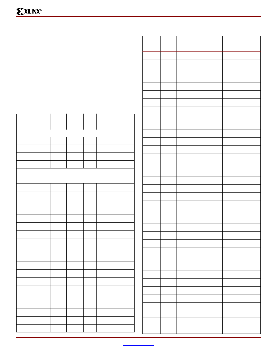
VirtexTM-E 1.8 V Field Programmable Gate Arrays
R
DS022-4 (v2.5) March 14, 2003
www.xilinx.com
Module 4 of 4
Production Product Specification
1-800-255-7778
23
BG352 Differential Pin Pairs
Virtex-E devices have differential pin pairs that can also pro-
vide other functions when not used as a differential pair. A
check (
) in the AO column indicates that the pin pair can be
used as an asynchronous output for all devices provided in
this package. Pairs with a note number in the AO column
are device dependent. They can have asynchronous out-
puts if the pin pair are in the same CLB row and column in
the device. Numbers in this column refer to footnotes that
indicate which devices have pin pairs than can be asynchro-
nous outputs. The Other Functions column indicates alter-
native function(s) not available when the pair is used as a
differential pair or differential clock
Table 11: BG352 Differential Pin Pair Summary
XCV100E, XCV200E, XCV300E
Pair
Bank
P
Pin
N
Pin
AO
Other
Functions
Global Differential Clock
0
4
AE13
AC13
NA
IO LVDS 55
1
5
AF14
AD14
NA
IO LVDS 55
2
1
B14
A13
NA
IO LVDS 9
3
0
D14
A15
NA
IO LVDS 9
IO LVDS
Total Outputs: 87, Asynchronous Output Pairs: 43
0
0
B23
D21
VREF_0
1
0
D20
A23
-
2
0
B22
C21
VREF_0
3
0
A21
B20
2
-
4
0
B19
C19
VREF_0
5
0
C18
D17
-
6
0
A18
C17
2
-
7
0
C16
B17
-
8
0
D15
A16
VREF_0
9
1
A13
A15
GCLK LVDS 3/2
10
1
A12
C13
2
-
11
1
C12
B12
VREF_1
12
1
B11
A11
-
13
1
D11
C11
2
-
14
1
C10
B9
-
15
1
C9
B8
VREF_1
16
1
A7
D9
1
-
17
1
B6
A6
VREF_1
18
1
A4
C7
-
19
1
D6
C6
VREF_1
20
1
C4
D5
CS
21
2
E4
D3
DIN_D0
22
2
D2
C1
VREF_2
23
2
G4
F3
-
24
2
E2
F2
VREF_2
25
2
F1
J4
2
-
26
2
H2
G1
D1
27
2
J3
J2
D2
28
2
J1
L4
1
-
29
2
L3
L2
-
30
2
M4
M3
D3
31
2
M2
M1
2
-
32
2
N4
N2
-
33
3
R1
R2
2
-
34
3
R3
R4
VREF_3
35
3
T2
U2
-
36
3
T4
V1
1
-
37
3
U3
U4
D5
38
3
V3
V4
VREF_3
39
3
Y1
Y2
1
-
40
3
AA2
Y3
VREF_3
41
3
AC1
AB2
-
42
3
AA4
AC2
VREF_3
43
3
AC3
AD2
INIT
44
4
AC5
AD4
-
45
4
AE4
AF3
VREF_4
46
4
AC7
AD6
-
47
4
AE5
AE6
VREF_4
48
4
AF6
AC9
2
-
49
4
AE8
AF7
VREF_4
50
4
AD9
AE9
-
51
4
AF9
AC11
2
-
52
4
AD11
AE11
-
53
4
AC12
AD12
VREF_4
54
4
AE12
AF12
2
-
Table 11: BG352 Differential Pin Pair Summary
XCV100E, XCV200E, XCV300E
Pair
Bank
P
Pin
N
Pin
AO
Other
Functions

VirtexTM-E 1.8 V Field Programmable Gate Arrays
R
Module 4 of 4
www.xilinx.com
DS022-4 (v2.5) March 14, 2003
24
1-800-255-7778
Production Product Specification
BG432 Ball Grid Array Packages
XCV300E, XCV400E, and XCV600E devices in BG432 Ball
Grid Array packages have footprint compatibility. Pins
labeled I0_VREF can be used as either in all parts unless
device-dependent as indicated in the footnotes. If the pin is
not used as V
REF
, it can be used as general I/O. Immedi-
ately following
Table 12
, see
Table 13
for Differential Pair
information.
55
5
AC13
AD14
GCLK LVDS 1/0
56
5
AD15
AC15
VREF_5
57
5
AE16
AE17
-
58
5
AC16
AF18
2
-
59
5
AD17
AC17
-
60
5
AD18
AC18
VREF_5
61
5
AF20
AE20
1
-
62
5
AE21
AD20
VREF_5
63
5
AF23
AE22
-
64
5
AC21
AE23
VREF_5
65
6
AD25
AC24
-
66
6
AC26
AD26
VREF_6
67
6
AB25
AA24
-
68
6
Y24
AA25
VREF_6
69
6
W24
V23
2
-
70
6
U23
Y26
VREF_6
71
6
U24
V25
-
72
6
U25
T23
1
-
73
6
T26
T25
-
74
6
R25
R24
VREF_6
75
6
P24
R26
2
-
76
7
N24
N25
-
77
7
M24
M25
2
-
78
7
L26
M23
VREF_7
79
7
L24
K25
-
80
7
J25
J26
1
-
81
7
H25
K23
-
82
7
G26
J23
VREF_7
83
7
H24
G25
1
-
84
7
D26
G24
VREF_7
85
7
F24
E25
-
86
7
E24
D25
VREF_7
Notes:
1.
AO in the XCV100E.
2.
AO in the XCV200E.
Table 11: BG352 Differential Pin Pair Summary
XCV100E, XCV200E, XCV300E
Pair
Bank
P
Pin
N
Pin
AO
Other
Functions
Table 12: BG432 -- XCV300E, XCV400E, XCV600E
Bank
Pin Description
Pin #
0
GCK3
D17
0
IO
A22
0
IO
A26
0
IO
B20
0
IO
C23
0
IO
C28
0
IO_L0N_Y
B29
0
IO_L0P_Y
D27
0
IO_L1N_YY
B28
0
IO_L1P_YY
C27
0
IO_VREF_L2N_YY
D26
0
IO_L2P_YY
A28
0
IO_L3N_Y
B27
0
IO_L3P_Y
C26
0
IO_L4N_YY
D25
0
IO_L4P_YY
A27
0
IO_VREF_L5N_YY
D24
0
IO_L5P_YY
C25
0
IO_L6N_Y
B25
0
IO_L6P_Y
D23
0
IO_VREF_L7N_Y
C24
1
0
IO_L7P_Y
B24
0
IO_VREF_L8N_YY
D22
0
IO_L8P_YY
A24
0
IO_L9N_YY
C22
0
IO_L9P_YY
B22
0
IO_L10N_YY
C21
0
IO_L10P_YY
D20
0
IO_L11N_YY
B21
0
IO_L11P_YY
C20
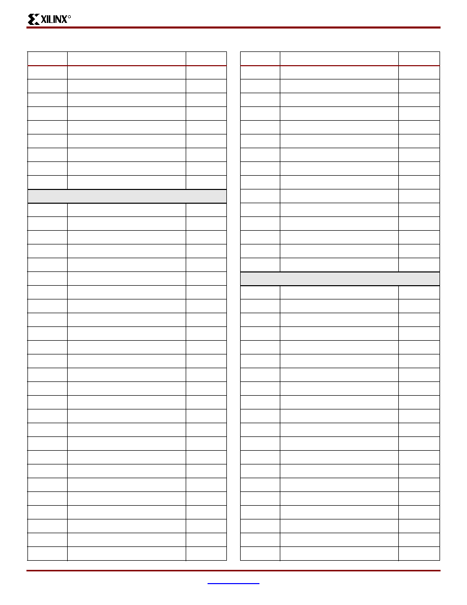
VirtexTM-E 1.8 V Field Programmable Gate Arrays
R
DS022-4 (v2.5) March 14, 2003
www.xilinx.com
Module 4 of 4
Production Product Specification
1-800-255-7778
25
0
IO_L12N_YY
A20
0
IO_L12P_YY
D19
0
IO_VREF_L13N_YY
B19
0
IO_L13P_YY
A19
0
IO_L14N_Y
B18
0
IO_L14P_Y
D18
0
IO_VREF_L15N_Y
C18
2
0
IO_L15P_Y
B17
0
IO_LVDS_DLL_L16N
C17
1
GCK2
A16
1
IO
A12
1
IO
B9
1
IO
B11
1
IO
C16
1
IO
D9
1
IO_LVDS_DLL_L16P
B16
1
IO_L17N_Y
A15
1
IO_VREF_L17P_Y
B15
2
1
IO_L18N_Y
C15
1
IO_L18P_Y
D15
1
IO_L19N_YY
B14
1
IO_VREF_L19P_YY
A13
1
IO_L20N_YY
B13
1
IO_L20P_YY
D14
1
IO_L21N_YY
C13
1
IO_L21P_YY
B12
1
IO_L22N_YY
D13
1
IO_L22P_YY
C12
1
IO_L23N_YY
D12
1
IO_L23P_YY
C11
1
IO_L24N_YY
B10
1
IO_VREF_L24P_YY
C10
1
IO_L25N_Y
C9
1
IO_VREF_L25P_Y
D10
1
1
IO_L26N_Y
A8
Table 12: BG432 -- XCV300E, XCV400E, XCV600E
Bank
Pin Description
Pin #
1
IO_L26P_Y
B8
1
IO_L27N_YY
C8
1
IO_VREF_L27P_YY
B7
1
IO_L28N_YY
D8
1
IO_L28P_YY
A6
1
IO_L29N_Y
B6
1
IO_L29P_Y
D7
1
IO_L30N_YY
A5
1
IO_VREF_L30P_YY
C6
1
IO_L31N_YY
B5
1
IO_L31P_YY
D6
1
IO_L32N_Y
A4
1
IO_L32P_Y
C5
1
IO_WRITE_L33N_YY
B4
1
IO_CS_L33P_YY
D5
2
IO
H4
2
IO
J3
2
IO
L3
2
IO
M1
2
IO
R2
2
IO_DOUT_BUSY_L34P_YY
D3
2
IO_DIN_D0_L34N_YY
C2
2
IO_L35P
D2
2
IO_L35N
E4
2
IO_L36P_Y
D1
2
IO_L36N_Y
E3
2
IO_VREF_L37P_Y
E2
2
IO_L37N_Y
F4
2
IO_L38P
E1
2
IO_L38N
F3
2
IO_L39P_Y
F2
2
IO_L39N_Y
G4
2
IO_VREF_L40P_YY
G3
2
IO_L40N_YY
G2
2
IO_L41P_Y
H3
Table 12: BG432 -- XCV300E, XCV400E, XCV600E
Bank
Pin Description
Pin #
VirtexTM-E 1.8 V Field Programmable Gate Arrays
R
Module 4 of 4
www.xilinx.com
DS022-4 (v2.5) March 14, 2003
26
1-800-255-7778
Production Product Specification
2
IO_L41N_Y
H2
2
IO_VREF_L42P_Y
H1
1
2
IO_L42N_Y
J4
2
IO_VREF_L43P_YY
J2
2
IO_D1_L43N_YY
K4
2
IO_D2_L44P_YY
K2
2
IO_L44N_YY
K1
2
IO_L45P_Y
L2
2
IO_L45N_Y
M4
2
IO_L46P_Y
M3
2
IO_L46N_Y
M2
2
IO_L47P_Y
N4
2
IO_L47N_Y
N3
2
IO_VREF_L48P_YY
N1
2
IO_D3_L48N_YY
P4
2
IO_L49P_Y
P3
2
IO_L49N_Y
P2
2
IO_VREF_L50P_Y
R3
2
2
IO_L50N_Y
R4
2
IO_L51P_YY
R1
2
IO_L51N_YY
T3
3
IO
AA2
3
IO
AC2
3
IO
AE2
3
IO
U3
3
IO
W1
3
IO_L52P_Y
U4
3
IO_VREF_L52N_Y
U2
2
3
IO_L53P_Y
U1
3
IO_L53N_Y
V3
3
IO_D4_L54P_YY
V4
3
IO_VREF_L54N_YY
V2
3
IO_L55P_Y
W3
3
IO_L55N_Y
W4
3
IO_L56P_Y
Y1
Table 12: BG432 -- XCV300E, XCV400E, XCV600E
Bank
Pin Description
Pin #
3
IO_L56N_Y
Y3
3
IO_L57P_Y
Y4
3
IO_L57N_Y
Y2
3
IO_L58P_YY
AA3
3
IO_D5_L58N_YY
AB1
3
IO_D6_L59P_YY
AB3
3
IO_VREF_L59N_YY
AB4
3
IO_L60P_Y
AD1
3
IO_VREF_L60N_Y
AC3
1
3
IO_L61P_Y
AC4
3
IO_L61N_Y
AD2
3
IO_L62P_YY
AD3
3
IO_VREF_L62N_YY
AD4
3
IO_L63P_Y
AF2
3
IO_L63N_Y
AE3
3
IO_L64P
AE4
3
IO_L64N
AG1
3
IO_L65P_Y
AG2
3
IO_VREF_L65N_Y
AF3
3
IO_L66P_Y
AF4
3
IO_L66N_Y
AH1
3
IO_L67P
AH2
3
IO_L67N
AG3
3
IO_D7_L68P_YY
AG4
3
IO_INIT_L68N_YY
AJ2
3
IO
T2
4
GCK0
AL16
4
IO
AH10
4
IO
AJ11
4
IO
AK7
4
IO
AL12
4
IO
AL15
4
IO_L69P_YY
AJ4
4
IO_L69N_YY
AK3
4
IO_L70P_Y
AH5
Table 12: BG432 -- XCV300E, XCV400E, XCV600E
Bank
Pin Description
Pin #

VirtexTM-E 1.8 V Field Programmable Gate Arrays
R
DS022-4 (v2.5) March 14, 2003
www.xilinx.com
Module 4 of 4
Production Product Specification
1-800-255-7778
27
4
IO_L70N_Y
AK4
4
IO_L71P_YY
AJ5
4
IO_L71N_YY
AH6
4
IO_VREF_L72P_YY
AL4
4
IO_L72N_YY
AK5
4
IO_L73P_Y
AJ6
4
IO_L73N_Y
AH7
4
IO_L74P_YY
AL5
4
IO_L74N_YY
AK6
4
IO_VREF_L75P_YY
AJ7
4
IO_L75N_YY
AL6
4
IO_L76P_Y
AH9
4
IO_L76N_Y
AJ8
4
IO_VREF_L77P_Y
AK8
1
4
IO_L77N_Y
AJ9
4
IO_VREF_L78P_YY
AL8
4
IO_L78N_YY
AK9
4
IO_L79P_YY
AK10
4
IO_L79N_YY
AL10
4
IO_L80P_YY
AH12
4
IO_L80N_YY
AK11
4
IO_L81P_YY
AJ12
4
IO_L81N_YY
AK12
4
IO_L82P_YY
AH13
4
IO_L82N_YY
AJ13
4
IO_VREF_L83P_YY
AL13
4
IO_L83N_YY
AK14
4
IO_L84P_Y
AH14
4
IO_L84N_Y
AJ14
4
IO_VREF_L85P_Y
AK15
2
4
IO_L85N_Y
AJ15
4
IO_LVDS_DLL_L86P
AH15
5
GCK1
AK16
5
IO
AH20
5
IO
AJ19
Table 12: BG432 -- XCV300E, XCV400E, XCV600E
Bank
Pin Description
Pin #
5
IO
AJ23
5
IO
AJ24
5
IO_LVDS_DLL_L86N
AL17
5
IO_L87P_Y
AK17
5
IO_VREF_L87N_Y
AJ17
2
5
IO_L88P_Y
AH17
5
IO_L88N_Y
AK18
5
IO_L89P_YY
AL19
5
IO_VREF_L89N_YY
AJ18
5
IO_L90P_YY
AH18
5
IO_L90N_YY
AL20
5
IO_L91P_YY
AK20
5
IO_L91N_YY
AH19
5
IO_L92P_YY
AJ20
5
IO_L92N_YY
AK21
5
IO_L93P_YY
AJ21
5
IO_L93N_YY
AL22
5
IO_L94P_YY
AJ22
5
IO_VREF_L94N_YY
AK23
5
IO_L95P_Y
AH22
5
IO_VREF_L95N_Y
AL24
1
5
IO_L96P_Y
AK24
5
IO_L96N_Y
AH23
5
IO_L97P_YY
AK25
5
IO_VREF_L97N_YY
AJ25
5
IO_L98P_YY
AL26
5
IO_L98N_YY
AK26
5
IO_L99P_Y
AH25
5
IO_L99N_Y
AL27
5
IO_L100P_YY
AJ26
5
IO_VREF_L100N_YY
AK27
5
IO_L101P_YY
AH26
5
IO_L101N_YY
AL28
5
IO_L102P_Y
AJ27
5
IO_L102N_Y
AK28
Table 12: BG432 -- XCV300E, XCV400E, XCV600E
Bank
Pin Description
Pin #

VirtexTM-E 1.8 V Field Programmable Gate Arrays
R
Module 4 of 4
www.xilinx.com
DS022-4 (v2.5) March 14, 2003
28
1-800-255-7778
Production Product Specification
6
IO
AA30
6
IO
AC30
6
IO
AD29
6
IO
U31
6
IO
W28
6
IO_L103N_YY
AJ30
6
IO_L103P_YY
AH30
6
IO_L104N
AG28
6
IO_L104P
AH31
6
IO_L105N_Y
AG29
6
IO_L105P_Y
AG30
6
IO_VREF_L106N_Y
AF28
6
IO_L106P_Y
AG31
6
IO_L107N
AF29
6
IO_L107P
AF30
6
IO_L108N_Y
AE28
6
IO_L108P_Y
AF31
6
IO_VREF_L109N_YY
AE30
6
IO_L109P_YY
AD28
6
IO_L110N_Y
AD30
6
IO_L110P_Y
AD31
6
IO_VREF_L111N_Y
AC28
1
6
IO_L111P_Y
AC29
6
IO_VREF_L112N_YY
AB28
6
IO_L112P_YY
AB29
6
IO_L113N_YY
AB31
6
IO_L113P_YY
AA29
6
IO_L114N_Y
Y28
6
IO_L114P_Y
Y29
6
IO_L115N_Y
Y30
6
IO_L115P_Y
Y31
6
IO_L116N_Y
W29
6
IO_L116P_Y
W30
6
IO_VREF_L117N_YY
V28
6
IO_L117P_YY
V29
6
IO_L118N_Y
V30
Table 12: BG432 -- XCV300E, XCV400E, XCV600E
Bank
Pin Description
Pin #
6
IO_L118P_Y
U29
6
IO_VREF_L119N_Y
U28
2
6
IO_L119P_Y
U30
6
IO
T30
7
IO
C30
7
IO
H29
7
IO
H31
7
IO
L29
7
IO
M31
7
IO
R28
7
IO_L120N_YY
T31
7
IO_L120P_YY
R29
7
IO_L121N_Y
R30
7
IO_VREF_L121P_Y
R31
2
7
IO_L122N_Y
P29
7
IO_L122P_Y
P28
7
IO_L123N_YY
P30
7
IO_VREF_L123P_YY
N30
7
IO_L124N_Y
N28
7
IO_L124P_Y
N31
7
IO_L125N_Y
M29
7
IO_L125P_Y
M28
7
IO_L126N_Y
M30
7
IO_L126P_Y
L30
7
IO_L127N_YY
K31
7
IO_L127P_YY
K30
7
IO_L128N_YY
K28
7
IO_VREF_L128P_YY
J30
7
IO_L129N_Y
J29
7
IO_VREF_L129P_Y
J28
1
7
IO_L130N_Y
H30
7
IO_L130P_Y
G30
7
IO_L131N_YY
H28
7
IO_VREF_L131P_YY
F31
7
IO_L132N_Y
G29
Table 12: BG432 -- XCV300E, XCV400E, XCV600E
Bank
Pin Description
Pin #
VirtexTM-E 1.8 V Field Programmable Gate Arrays
R
DS022-4 (v2.5) March 14, 2003
www.xilinx.com
Module 4 of 4
Production Product Specification
1-800-255-7778
29
7
IO_L132P_Y
G28
7
IO_L133N
E31
7
IO_L133P
E30
7
IO_L134N_Y
F29
7
IO_VREF_L134P_Y
F28
7
IO_L135N_Y
D31
7
IO_L135P_Y
D30
7
IO_L136N
E29
7
IO_L136P
E28
2
CCLK
D4
3
DONE
AH4
NA
DXN
AH27
NA
DXP
AK29
NA
M0
AH28
NA
M1
AH29
NA
M2
AJ28
NA
PROGRAM
AH3
NA
TCK
D28
NA
TDI
B3
2
TDO
C4
NA
TMS
D29
NA
VCCINT
A10
NA
VCCINT
A17
NA
VCCINT
B23
NA
VCCINT
B26
NA
VCCINT
C7
NA
VCCINT
C14
NA
VCCINT
C19
NA
VCCINT
F1
NA
VCCINT
F30
NA
VCCINT
K3
NA
VCCINT
K29
NA
VCCINT
N2
NA
VCCINT
N29
Table 12: BG432 -- XCV300E, XCV400E, XCV600E
Bank
Pin Description
Pin #
NA
VCCINT
T1
NA
VCCINT
T29
NA
VCCINT
W2
NA
VCCINT
W31
NA
VCCINT
AB2
NA
VCCINT
AB30
NA
VCCINT
AE29
NA
VCCINT
AF1
NA
VCCINT
AH8
NA
VCCINT
AH24
NA
VCCINT
AJ10
NA
VCCINT
AJ16
NA
VCCINT
AK22
NA
VCCINT
AK13
NA
VCCINT
AK19
0
VCCO
A21
0
VCCO
C29
0
VCCO
D21
1
VCCO
A1
1
VCCO
A11
1
VCCO
D11
2
VCCO
C3
2
VCCO
L4
2
VCCO
L1
3
VCCO
AA1
3
VCCO
AA4
3
VCCO
AJ3
4
VCCO
AH11
4
VCCO
AL1
4
VCCO
AL11
5
VCCO
AH21
5
VCCO
AL21
5
VCCO
AJ29
6
VCCO
AA28
6
VCCO
AA31
Table 12: BG432 -- XCV300E, XCV400E, XCV600E
Bank
Pin Description
Pin #
VirtexTM-E 1.8 V Field Programmable Gate Arrays
R
Module 4 of 4
www.xilinx.com
DS022-4 (v2.5) March 14, 2003
30
1-800-255-7778
Production Product Specification
6
VCCO
AL31
7
VCCO
A31
7
VCCO
L28
7
VCCO
L31
NA
GND
A2
NA
GND
A3
NA
GND
A7
NA
GND
A9
NA
GND
A14
NA
GND
A18
NA
GND
A23
NA
GND
A25
NA
GND
A29
NA
GND
A30
NA
GND
B1
NA
GND
B2
NA
GND
B30
NA
GND
B31
NA
GND
C1
NA
GND
C31
NA
GND
D16
NA
GND
G1
NA
GND
G31
NA
GND
J1
NA
GND
J31
NA
GND
P1
NA
GND
P31
NA
GND
T4
NA
GND
T28
NA
GND
V1
NA
GND
V31
NA
GND
AC1
NA
GND
AC31
NA
GND
AE1
NA
GND
AE31
Table 12: BG432 -- XCV300E, XCV400E, XCV600E
Bank
Pin Description
Pin #
NA
GND
AH16
NA
GND
AJ1
NA
GND
AJ31
NA
GND
AK1
NA
GND
AK2
NA
GND
AK30
NA
GND
AK31
NA
GND
AL2
NA
GND
AL3
NA
GND
AL7
NA
GND
AL9
NA
GND
AL14
NA
GND
AL18
NA
GND
AL23
NA
GND
AL25
NA
GND
AL29
NA
GND
AL30
Notes:
1.
V
REF
or I/O option only in the XCV600E; otherwise, I/O
option only.
2.
V
REF
or I/O option only in the XCV400E, XCV600E;
otherwise, I/O option only.
Table 12: BG432 -- XCV300E, XCV400E, XCV600E
Bank
Pin Description
Pin #

VirtexTM-E 1.8 V Field Programmable Gate Arrays
R
DS022-4 (v2.5) March 14, 2003
www.xilinx.com
Module 4 of 4
Production Product Specification
1-800-255-7778
31
BG432 Differential Pin Pairs
Virtex-E devices have differential pin pairs that can also Vir-
tex-E devices have differential pin pairs that can also pro-
vide other functions when not used as a differential pair. A
in the AO column indicates that the pin pair can be used as
an asynchronous output for all devices provided in this
package. Pairs with a note number in the AO column are
device dependent. They can have asynchronous outputs if
the pin pair are in the same CLB row and column in the
device. Numbers in this column refer to footnotes that indi-
cate which devices have pin pairs than can be asynchro-
nous outputs. The Other Functions column indicates
alternative function(s) not available when the pair is used as
a differential pair or differential clock.
Table 13: BG432 Differential Pin Pair Summary
XCV300E, XCV400E, XC600E
Pair
Bank
P
Pin
N
Pin
AO
Other
Functions
Global Differential Clock
0
4
AL16
AH15
NA
IO_DLL_L86P
1
5
AK16
AL17
NA
IO_DLL_L86N
2
1
A16
B16
NA
IO_DLL_L16P
3
0
D17
C17
NA
IO_DLL_L16N
IO LVDS
Total Outputs: 137, Asynchronous Output Pairs: 63
0
0
D27
B29
1
-
1
0
C27
B28
-
2
0
A28
D26
VREF
3
0
C26
B27
2
-
4
0
A27
D25
-
5
0
C25
D24
VREF
6
0
D23
B25
1
-
7
0
B24
C24
1
VREF
8
0
A24
D22
VREF
9
0
B22
C22
-
10
0
D20
C21
-
11
0
C20
B21
-
12
0
D19
A20
-
13
0
A19
B19
VREF
14
0
D18
B18
1
-
15
0
B17
C18
1
VREF
16
1
B16
C17
NA
IO_LVDS_DLL
17
1
B15
A15
1
VREF
18
1
D15
C15
1
-
19
1
A13
B14
VREF
20
1
D14
B13
-
21
1
B12
C13
-
22
1
C12
D13
-
23
1
C11
D12
-
24
1
C10
B10
VREF
25
1
D10
C9
1
VREF
26
1
B8
A8
1
-
27
1
B7
C8
VREF
28
1
A6
D8
-
29
1
D7
B6
2
-
30
1
C6
A5
VREF
31
1
D6
B5
-
32
1
C5
A4
1
-
33
1
D5
B4
CS, WRITE
34
2
D3
C2
DIN, D0, BUSY
35
2
D2
E4
3
-
36
2
D1
E3
4
-
37
2
E2
F4
1
VREF
38
2
E1
F3
5
-
39
2
F2
G4
1
-
40
2
G3
G2
VREF
41
2
H3
H2
4
-
42
2
H1
J4
1
VREF
43
2
J2
K4
D1
44
2
K2
K1
D2
45
2
L2
M4
4
-
46
2
M3
M2
1
-
47
2
N4
N3
1
-
Table 13: BG432 Differential Pin Pair Summary
XCV300E, XCV400E, XC600E
Pair
Bank
P
Pin
N
Pin
AO
Other
Functions
VirtexTM-E 1.8 V Field Programmable Gate Arrays
R
Module 4 of 4
www.xilinx.com
DS022-4 (v2.5) March 14, 2003
32
1-800-255-7778
Production Product Specification
48
2
N1
P4
D3
49
2
P3
P2
4
-
50
2
R3
R4
1
VREF
51
2
R1
T3
-
52
3
U4
U2
1
VREF
53
3
U1
V3
4
-
54
3
V4
V2
VREF
55
3
W3
W4
1
-
56
3
Y1
Y3
1
-
57
3
Y4
Y2
4
-
58
3
AA3
AB1
D5
59
3
AB3
AB4
VREF
60
3
AD1
AC3
1
VREF
61
3
AC4
AD2
4
-
62
3
AD3
AD4
VREF
63
3
AF2
AE3
1
-
64
3
AE4
AG1
5
-
65
3
AG2
AF3
1
VREF
66
3
AF4
AH1
4
-
67
3
AH2
AG3
3
-
68
3
AG4
AJ2
INIT
69
4
AJ4
AK3
-
70
4
AH5
AK4
1
-
71
4
AJ5
AH6
-
72
4
AL4
AK5
VREF
73
4
AJ6
AH7
2
-
74
4
AL5
AK6
-
75
4
AJ7
AL6
VREF
76
4
AH9
AJ8
1
-
77
4
AK8
AJ9
1
VREF
78
4
AL8
AK9
VREF
79
4
AK10
AL10
-
Table 13: BG432 Differential Pin Pair Summary
XCV300E, XCV400E, XC600E
Pair
Bank
P
Pin
N
Pin
AO
Other
Functions
80
4
AH12
AK11
-
81
4
AJ12
AK12
-
82
4
AH13
AJ13
-
83
4
AL13
AK14
VREF
84
4
AH14
AJ14
1
-
85
4
AK15
AJ15
1
VREF
86
5
AH15
AL17
NA
IO_LVDS_DLL
87
5
AK17
AJ17
1
VREF
88
5
AH17
AK18
1
-
89
5
AL19
AJ18
VREF
90
5
AH18
AL20
-
91
5
AK20
AH19
-
92
5
AJ20
AK21
-
93
5
AJ21
AL22
-
94
5
AJ22
AK23
VREF
95
5
AH22
AL24
1
VREF
96
5
AK24
AH23
1
-
97
5
AK25
AJ25
VREF
98
5
AL26
AK26
-
99
5
AH25
AL27
2
-
100
5
AJ26
AK27
VREF
101
5
AH26
AL28
-
102
5
AJ27
AK28
1
-
103
6
AH30
AJ30
-
104
6
AH31
AG28
3
-
105
6
AG30
AG29
4
-
106
6
AG31
AF28
1
VREF
107
6
AF30
AF29
5
-
108
6
AF31
AE28
1
-
109
6
AD28
AE30
VREF
110
6
AD31
AD30
4
-
111
6
AC29
AC28
1
VREF
Table 13: BG432 Differential Pin Pair Summary
XCV300E, XCV400E, XC600E
Pair
Bank
P
Pin
N
Pin
AO
Other
Functions
VirtexTM-E 1.8 V Field Programmable Gate Arrays
R
DS022-4 (v2.5) March 14, 2003
www.xilinx.com
Module 4 of 4
Production Product Specification
1-800-255-7778
33
BG560 Ball Grid Array Packages
XCV1000E, XCV1600E, and XCV2000E devices in BG560
Ball Grid Array packages have footprint compatibility. Pins
labeled I0_VREF can be used as either in all parts unless
device-dependent as indicated in the footnotes. If the pin is
not used as V
REF
, it can be used as general I/O. Immedi-
ately following
Table 14
, see
Table 15
for Differential Pair
information.
112
6
AB29
AB28
VREF
113
6
AA29
AB31
-
114
6
Y29
Y28
4
-
115
6
Y31
Y30
1
-
116
6
W30
W29
1
-
117
6
V29
V28
VREF
118
6
U29
V30
4
-
119
6
U30
U28
1
VREF
120
7
R29
T31
-
121
7
R31
R30
1
VREF
122
7
P28
P29
4
-
123
7
N30
P30
VREF
124
7
N31
N28
1
-
125
7
M28
M29
1
-
126
7
L30
M30
4
-
127
7
K30
K31
-
128
7
J30
K28
VREF
129
7
J28
J29
1
VREF
130
7
G30
H30
4
-
131
7
F31
H28
VREF
132
7
G28
G29
1
-
133
7
E30
E31
5
-
134
7
F28
F29
1
VREF
135
7
D30
D31
4
-
136
7
E28
E29
3
-
Notes:
1.
AO in the XCV300E, 600E.
2.
AO in the XCV300E.
3.
AO in the XCV400E, 600E.
4.
AO in the XCV300E, 400E.
5.
AO in the XCV600E.
Table 13: BG432 Differential Pin Pair Summary
XCV300E, XCV400E, XC600E
Pair
Bank
P
Pin
N
Pin
AO
Other
Functions
Table 14: BG560 -- XCV400E, XCV600E, XCV1000E,
XCV1600E, XCV2000E
Bank
Pin Description
Pin#
See Note
0
GCK3
A17
0
IO
A27
0
IO
B25
0
IO
C28
0
IO
C30
0
IO
D30
0
IO_L0N
E28
0
IO_VREF_L0P
D29
3
0
IO_L1N_YY
D28
0
IO_L1P_YY
A31
0
IO_VREF_L2N_YY
E27
0
IO_L2P_YY
C29
0
IO_L3N_Y
B30
0
IO_L3P_Y
D27
0
IO_L4N_YY
E26
0
IO_L4P_YY
B29
0
IO_VREF_L5N_YY
D26
0
IO_L5P_YY
C27
0
IO_L6N_Y
E25
0
IO_VREF_L6P_Y
A28
1
0
IO_L7N_Y
D25
0
IO_L7P_Y
C26
0
IO_VREF_L8N_Y
E24
4
0
IO_L8P_Y
B26
0
IO_L9N_Y
C25
0
IO_L9P_Y
D24
0
IO_VREF_L10N_YY
E23
0
IO_L10P_YY
A25
0
IO_L11N_YY
D23
VirtexTM-E 1.8 V Field Programmable Gate Arrays
R
Module 4 of 4
www.xilinx.com
DS022-4 (v2.5) March 14, 2003
34
1-800-255-7778
Production Product Specification
0
IO_L11P_YY
B24
0
IO_L12N_Y
E22
0
IO_L12P_Y
C23
0
IO_L13N_YY
A23
0
IO_L13P_YY
D22
0
IO_VREF_L14N_YY
E21
3
0
IO_L14P_YY
B22
0
IO_L15N_Y
D21
0
IO_L15P_Y
C21
0
IO_L16N_YY
B21
0
IO_L16P_YY
E20
0
IO_VREF_L17N_YY
D20
0
IO_L17P_YY
C20
0
IO_L18N_Y
B20
0
IO_L18P_Y
E19
0
IO_L19N_Y
D19
0
IO_L19P_Y
C19
0
IO_VREF_L20N_Y
A19
0
IO_L20P_Y
D18
0
IO_LVDS_DLL_L21N
C18
0
IO_VREF
E18
2
1
GCK2
D17
1
IO
A3
1
IO
D9
1
IO
E8
1
IO
E11
1
IO_LVDS_DLL_L21P
E17
1
IO_VREF_L22N_Y
C17
2
1
IO_L22P_Y
B17
1
IO_L23N_Y
B16
1
IO_VREF_L23P_Y
D16
1
IO_L24N_Y
E16
1
IO_L24P_Y
C16
1
IO_L25N_Y
A15
Table 14: BG560 -- XCV400E, XCV600E, XCV1000E,
XCV1600E, XCV2000E
Bank
Pin Description
Pin#
See Note
1
IO_L25P_Y
C15
1
IO_L26N_YY
D15
1
IO_VREF_L26P_YY
E15
1
IO_L27N_YY
C14
1
IO_L27P_YY
D14
1
IO_L28N_Y
A13
1
IO_L28P_Y
E14
1
IO_L29N_YY
C13
1
IO_VREF_L29P_YY
D13
3
1
IO_L30N_YY
C12
1
IO_L30P_YY
E13
1
IO_L31N_Y
A11
1
IO_L31P_Y
D12
1
IO_L32N_YY
B11
1
IO_L32P_YY
C11
1
IO_L33N_YY
B10
1
IO_VREF_L33P_YY
D11
1
IO_L34N_Y
C10
1
IO_L34P_Y
A9
1
IO_L35N_Y
C9
1
IO_VREF_L35P_Y
D10
4
1
IO_L36N_Y
A8
1
IO_L36P_Y
B8
1
IO_L37N_Y
E10
1
IO_VREF_L37P_Y
C8
1
1
IO_L38N_YY
B7
1
IO_VREF_L38P_YY
A6
1
IO_L39N_YY
C7
1
IO_L39P_YY
D8
1
IO_L40N_Y
A5
1
IO_L40P_Y
B5
1
IO_L41N_YY
C6
1
IO_VREF_L41P_YY
D7
1
IO_L42N_YY
A4
1
IO_L42P_YY
B4
Table 14: BG560 -- XCV400E, XCV600E, XCV1000E,
XCV1600E, XCV2000E
Bank
Pin Description
Pin#
See Note

VirtexTM-E 1.8 V Field Programmable Gate Arrays
R
DS022-4 (v2.5) March 14, 2003
www.xilinx.com
Module 4 of 4
Production Product Specification
1-800-255-7778
35
1
IO_L43N_Y
C5
1
IO_VREF_L43P_Y
E7
3
1
IO_WRITE_L44N_YY
D6
1
IO_CS_L44P_YY
A2
2
IO
D3
2
IO
F3
2
IO
G1
2
IO
J2
2
IO_DOUT_BUSY_L45P_YY
D4
2
IO_DIN_D0_L45N_YY
E4
2
IO_L46P_Y
F5
2
IO_VREF_L46N_Y
B3
3
2
IO_L47P_Y
F4
2
IO_L47N_Y
C1
2
IO_VREF_L48P_Y
G5
2
IO_L48N_Y
E3
2
IO_L49P_Y
D2
2
IO_L49N_Y
G4
2
IO_L50P_Y
H5
2
IO_L50N_Y
E2
2
IO_VREF_L51P_YY
H4
2
IO_L51N_YY
G3
2
IO_L52P_Y
J5
2
IO_VREF_L52N_Y
F1
1
2
IO_L53P_Y
J4
2
IO_L53N_Y
H3
2
IO_VREF_L54P_Y
K5
4
2
IO_L54N_Y
H2
2
IO_L55P_Y
J3
2
IO_L55N_Y
K4
2
IO_VREF_L56P_YY
L5
2
IO_D1_L56N_YY
K3
2
IO_D2_L57P_YY
L4
2
IO_L57N_YY
K2
Table 14: BG560 -- XCV400E, XCV600E, XCV1000E,
XCV1600E, XCV2000E
Bank
Pin Description
Pin#
See Note
2
IO_L58P_Y
M5
2
IO_L58N_Y
L3
2
IO_L59P_Y
L1
2
IO_L59N_Y
M4
2
IO_VREF_L60P_Y
N5
3
2
IO_L60N_Y
M2
2
IO_L61P_Y
N4
2
IO_L61N_Y
N3
2
IO_L62P_Y
N2
2
IO_L62N_Y
P5
2
IO_VREF_L63P_YY
P4
2
IO_D3_L63N_YY
P3
2
IO_L64P_Y
P2
2
IO_L64N_Y
R5
2
IO_L65P_Y
R4
2
IO_L65N_Y
R3
2
IO_VREF_L66P_Y
R1
2
IO_L66N_Y
T4
2
IO_L67P_Y
T5
2
IO_VREF_L67N_Y
T3
2
2
IO_L68P_YY
T2
2
IO_L68N_YY
U3
3
IO
AE3
3
IO
AF3
3
IO
AH3
3
IO
AK3
3
IO_VREF_L69P_Y
U1
2
3
IO_L69N_Y
U2
3
IO_L70P_Y
V2
3
IO_VREF_L70N_Y
V4
3
IO_L71P_Y
V5
3
IO_L71N_Y
V3
3
IO_L72P_Y
W1
3
IO_L72N_Y
W3
Table 14: BG560 -- XCV400E, XCV600E, XCV1000E,
XCV1600E, XCV2000E
Bank
Pin Description
Pin#
See Note

VirtexTM-E 1.8 V Field Programmable Gate Arrays
R
Module 4 of 4
www.xilinx.com
DS022-4 (v2.5) March 14, 2003
36
1-800-255-7778
Production Product Specification
3
IO_D4_L73P_YY
W4
3
IO_VREF_L73N_YY
W5
3
IO_L74P_Y
Y3
3
IO_L74N_Y
Y4
3
IO_L75P_Y
AA1
3
IO_L75N_Y
Y5
3
IO_L76P_Y
AA3
3
IO_VREF_L76N_Y
AA4
3
3
IO_L77P_Y
AB3
3
IO_L77N_Y
AA5
3
IO_L78P_Y
AC1
3
IO_L78N_Y
AB4
3
IO_L79P_YY
AC3
3
IO_D5_L79N_YY
AB5
3
IO_D6_L80P_YY
AC4
3
IO_VREF_L80N_YY
AD3
3
IO_L81P_Y
AE1
3
IO_L81N_Y
AC5
3
IO_L82P_Y
AD4
3
IO_VREF_L82N_Y
AF1
4
3
IO_L83P_Y
AF2
3
IO_L83N_Y
AD5
3
IO_L84P_Y
AG2
3
IO_VREF_L84N_Y
AE4
1
3
IO_L85P_YY
AH1
3
IO_VREF_L85N_YY
AE5
3
IO_L86P_Y
AF4
3
IO_L86N_Y
AJ1
3
IO_L87P_Y
AJ2
3
IO_L87N_Y
AF5
3
IO_L88P_Y
AG4
3
IO_VREF_L88N_Y
AK2
3
IO_L89P_Y
AJ3
3
IO_L89N_Y
AG5
3
IO_L90P_Y
AL1
Table 14: BG560 -- XCV400E, XCV600E, XCV1000E,
XCV1600E, XCV2000E
Bank
Pin Description
Pin#
See Note
3
IO_VREF_L90N_Y
AH4
3
3
IO_D7_L91P_YY
AJ4
3
IO_INIT_L91N_YY
AH5
3
IO
U4
4
GCK0
AL17
4
IO
AJ8
4
IO
AJ11
4
IO
AK6
4
IO
AK9
4
IO_L92P_YY
AL4
4
IO_L92N_YY
AJ6
4
IO_L93P_Y
AK5
4
IO_VREF_L93N_Y
AN3
3
4
IO_L94P_YY
AL5
4
IO_L94N_YY
AJ7
4
IO_VREF_L95P_YY
AM4
4
IO_L95N_YY
AM5
4
IO_L96P_Y
AK7
4
IO_L96N_Y
AL6
4
IO_L97P_YY
AM6
4
IO_L97N_YY
AN6
4
IO_VREF_L98P_YY
AL7
4
IO_L98N_YY
AJ9
4
IO_L99P_Y
AN7
4
IO_VREF_L99N_Y
AL8
1
4
IO_L100P_Y
AM8
4
IO_L100N_Y
AJ10
4
IO_VREF_L101P_Y
AL9
4
4
IO_L101N_Y
AM9
4
IO_L102P_Y
AK10
4
IO_L102N_Y
AN9
4
IO_VREF_L103P_YY
AL10
4
IO_L103N_YY
AM10
4
IO_L104P_YY
AL11
Table 14: BG560 -- XCV400E, XCV600E, XCV1000E,
XCV1600E, XCV2000E
Bank
Pin Description
Pin#
See Note
VirtexTM-E 1.8 V Field Programmable Gate Arrays
R
DS022-4 (v2.5) March 14, 2003
www.xilinx.com
Module 4 of 4
Production Product Specification
1-800-255-7778
37
4
IO_L104N_YY
AJ12
4
IO_L105P_Y
AN11
4
IO_L105N_Y
AK12
4
IO_L106P_YY
AL12
4
IO_L106N_YY
AM12
4
IO_VREF_L107P_YY
AK13
3
4
IO_L107N_YY
AL13
4
IO_L108P_Y
AM13
4
IO_L108N_Y
AN13
4
IO_L109P_YY
AJ14
4
IO_L109N_YY
AK14
4
IO_VREF_L110P_YY
AM14
4
IO_L110N_YY
AN15
4
IO_L111P_Y
AJ15
4
IO_L111N_Y
AK15
4
IO_L112P_Y
AL15
4
IO_L112N_Y
AM16
4
IO_VREF_L113P_Y
AL16
4
IO_L113N_Y
AJ16
4
IO_L114P_Y
AK16
4
IO_VREF_L114N_Y
AN17
2
4
IO_LVDS_DLL_L115P
AM17
5
GCK1
AJ17
5
IO
AL25
5
IO
AL28
5
IO
AL30
5
IO
AN28
5
IO_LVDS_DLL_L115N
AM18
5
IO_VREF
AL18
2
5
IO_L116P_Y
AK18
5
IO_VREF_L116N_Y
AJ18
5
IO_L117P_Y
AN19
5
IO_L117N_Y
AL19
5
IO_L118P_Y
AK19
Table 14: BG560 -- XCV400E, XCV600E, XCV1000E,
XCV1600E, XCV2000E
Bank
Pin Description
Pin#
See Note
5
IO_L118N_Y
AM20
5
IO_L119P_YY
AJ19
5
IO_VREF_L119N_YY
AL20
5
IO_L120P_YY
AN21
5
IO_L120N_YY
AL21
5
IO_L121P_Y
AJ20
5
IO_L121N_Y
AM22
5
IO_L122P_YY
AK21
5
IO_VREF_L122N_YY
AN23
3
5
IO_L123P_YY
AJ21
5
IO_L123N_YY
AM23
5
IO_L124P_Y
AK22
5
IO_L124N_Y
AM24
5
IO_L125P_YY
AL23
5
IO_L125N_YY
AJ22
5
IO_L126P_YY
AK23
5
IO_VREF_L126N_YY
AL24
5
IO_L127P_Y
AN26
5
IO_L127N_Y
AJ23
5
IO_L128P_Y
AK24
5
IO_VREF_L128N_Y
AM26
4
5
IO_L129P_Y
AM27
5
IO_L129N_Y
AJ24
5
IO_L130P_Y
AL26
5
IO_VREF_L130N_Y
AK25
1
5
IO_L131P_YY
AN29
5
IO_VREF_L131N_YY
AJ25
5
IO_L132P_YY
AK26
5
IO_L132N_YY
AM29
5
IO_L133P_Y
AM30
5
IO_L133N_Y
AJ26
5
IO_L134P_YY
AK27
5
IO_VREF_L134N_YY
AL29
5
IO_L135P_YY
AN31
5
IO_L135N_YY
AJ27
Table 14: BG560 -- XCV400E, XCV600E, XCV1000E,
XCV1600E, XCV2000E
Bank
Pin Description
Pin#
See Note
VirtexTM-E 1.8 V Field Programmable Gate Arrays
R
Module 4 of 4
www.xilinx.com
DS022-4 (v2.5) March 14, 2003
38
1-800-255-7778
Production Product Specification
5
IO_L136P_Y
AM31
5
IO_VREF_L136N_Y
AK28
3
6
IO
AE33
6
IO
AF31
6
IO
AJ32
6
IO
AL33
6
IO_L137N_YY
AH29
6
IO_L137P_YY
AJ30
6
IO_L138N_Y
AK31
6
IO_VREF_L138P_Y
AH30
3
6
IO_L139N_Y
AG29
6
IO_L139P_Y
AJ31
6
IO_VREF_L140N_Y
AK32
6
IO_L140P_Y
AG30
6
IO_L141N_Y
AH31
6
IO_L141P_Y
AF29
6
IO_L142N_Y
AH32
6
IO_L142P_Y
AF30
6
IO_VREF_L143N_YY
AE29
6
IO_L143P_YY
AH33
6
IO_L144N_Y
AG33
6
IO_VREF_L144P_Y
AE30
1
6
IO_L145N_Y
AD29
6
IO_L145P_Y
AF32
6
IO_VREF_L146N_Y
AE31
4
6
IO_L146P_Y
AD30
6
IO_L147N_Y
AE32
6
IO_L147P_Y
AC29
6
IO_VREF_L148N_YY
AD31
6
IO_L148P_YY
AC30
6
IO_L149N_YY
AB29
6
IO_L149P_YY
AC31
6
IO_L150N_Y
AC33
6
IO_L150P_Y
AB30
Table 14: BG560 -- XCV400E, XCV600E, XCV1000E,
XCV1600E, XCV2000E
Bank
Pin Description
Pin#
See Note
6
IO_L151N_Y
AB31
6
IO_L151P_Y
AA29
6
IO_VREF_L152N_Y
AA30
3
6
IO_L152P_Y
AA31
6
IO_L153N_Y
AA32
6
IO_L153P_Y
Y29
6
IO_L154N_Y
AA33
6
IO_L154P_Y
Y30
6
IO_VREF_L155N_YY
Y32
6
IO_L155P_YY
W29
6
IO_L156N_Y
W30
6
IO_L156P_Y
W31
6
IO_L157N_Y
W33
6
IO_L157P_Y
V30
6
IO_VREF_L158N_Y
V29
6
IO_L158P_Y
V31
6
IO_L159N_Y
V32
6
IO_VREF_L159P_Y
U33
2
6
IO
U29
7
IO
E30
7
IO
F29
7
IO
F33
7
IO
G30
7
IO
K30
7
IO_L160N_YY
U31
7
IO_L160P_YY
U32
7
IO_VREF_L161N_Y
T32
2
7
IO_L161P_Y
T30
7
IO_L162N_Y
T29
7
IO_VREF_L162P_Y
T31
7
IO_L163N_Y
R33
7
IO_L163P_Y
R31
7
IO_L164N_Y
R30
7
IO_L164P_Y
R29
Table 14: BG560 -- XCV400E, XCV600E, XCV1000E,
XCV1600E, XCV2000E
Bank
Pin Description
Pin#
See Note

VirtexTM-E 1.8 V Field Programmable Gate Arrays
R
DS022-4 (v2.5) March 14, 2003
www.xilinx.com
Module 4 of 4
Production Product Specification
1-800-255-7778
39
7
IO_L165N_YY
P32
7
IO_VREF_L165P_YY
P31
7
IO_L166N_Y
P30
7
IO_L166P_Y
P29
7
IO_L167N_Y
M32
7
IO_L167P_Y
N31
7
IO_L168N_Y
N30
7
IO_VREF_L168P_Y
L33
3
7
IO_L169N_Y
M31
7
IO_L169P_Y
L32
7
IO_L170N_Y
M30
7
IO_L170P_Y
L31
7
IO_L171N_YY
M29
7
IO_L171P_YY
J33
7
IO_L172N_YY
L30
7
IO_VREF_L172P_YY
K31
7
IO_L173N_Y
L29
7
IO_L173P_Y
H33
7
IO_L174N_Y
J31
7
IO_VREF_L174P_Y
H32
4
7
IO_L175N_Y
K29
7
IO_L175P_Y
H31
7
IO_L176N_Y
J30
7
IO_VREF_L176P_Y
G32
1
7
IO_L177N_YY
J29
7
IO_VREF_L177P_YY
G31
7
IO_L178N_Y
E33
7
IO_L178P_Y
E32
7
IO_L179N_Y
H29
7
IO_L179P_Y
F31
7
IO_L180N_Y
D32
7
IO_VREF_L180P_Y
E31
7
IO_L181N_Y
G29
7
IO_L181P_Y
C33
7
IO_L182N_Y
F30
Table 14: BG560 -- XCV400E, XCV600E, XCV1000E,
XCV1600E, XCV2000E
Bank
Pin Description
Pin#
See Note
7
IO_VREF_L182P_Y
D31
3
2
CCLK
C4
3
DONE
AJ5
NA
DXN
AK29
NA
DXP
AJ28
NA
M0
AJ29
NA
M1
AK30
NA
M2
AN32
NA
PROGRAM
AM1
NA
TCK
E29
NA
TDI
D5
2
TDO
E6
NA
TMS
B33
NA
NC
C31
NA
NC
AC2
NA
NC
AK4
NA
NC
AL3
NA
VCCINT
A21
NA
VCCINT
B12
NA
VCCINT
B14
NA
VCCINT
B18
NA
VCCINT
B28
NA
VCCINT
C22
NA
VCCINT
C24
NA
VCCINT
E9
NA
VCCINT
E12
NA
VCCINT
F2
NA
VCCINT
H30
NA
VCCINT
J1
NA
VCCINT
K32
NA
VCCINT
M3
NA
VCCINT
N1
Table 14: BG560 -- XCV400E, XCV600E, XCV1000E,
XCV1600E, XCV2000E
Bank
Pin Description
Pin#
See Note

VirtexTM-E 1.8 V Field Programmable Gate Arrays
R
Module 4 of 4
www.xilinx.com
DS022-4 (v2.5) March 14, 2003
40
1-800-255-7778
Production Product Specification
NA
VCCINT
N29
NA
VCCINT
N33
NA
VCCINT
U5
NA
VCCINT
U30
NA
VCCINT
Y2
NA
VCCINT
Y31
NA
VCCINT
AB2
NA
VCCINT
AB32
NA
VCCINT
AD2
NA
VCCINT
AD32
NA
VCCINT
AG3
NA
VCCINT
AG31
NA
VCCINT
AJ13
NA
VCCINT
AK8
NA
VCCINT
AK11
NA
VCCINT
AK17
NA
VCCINT
AK20
NA
VCCINT
AL14
NA
VCCINT
AL22
NA
VCCINT
AL27
NA
VCCINT
AN25
0
VCCO
A22
0
VCCO
A26
0
VCCO
A30
0
VCCO
B19
0
VCCO
B32
1
VCCO
A10
1
VCCO
A16
1
VCCO
B13
1
VCCO
C3
1
VCCO
E5
2
VCCO
B2
2
VCCO
D1
2
VCCO
H1
Table 14: BG560 -- XCV400E, XCV600E, XCV1000E,
XCV1600E, XCV2000E
Bank
Pin Description
Pin#
See Note
2
VCCO
M1
2
VCCO
R2
3
VCCO
V1
3
VCCO
AA2
3
VCCO
AD1
3
VCCO
AK1
3
VCCO
AL2
4
VCCO
AN4
4
VCCO
AN8
4
VCCO
AN12
4
VCCO
AM2
4
VCCO
AM15
5
VCCO
AL31
5
VCCO
AM21
5
VCCO
AN18
5
VCCO
AN24
5
VCCO
AN30
6
VCCO
W32
6
VCCO
AB33
6
VCCO
AF33
6
VCCO
AK33
6
VCCO
AM32
7
VCCO
C32
7
VCCO
D33
7
VCCO
K33
7
VCCO
N32
7
VCCO
T33
NA
GND
A1
NA
GND
A7
NA
GND
A12
NA
GND
A14
NA
GND
A18
NA
GND
A20
NA
GND
A24
Table 14: BG560 -- XCV400E, XCV600E, XCV1000E,
XCV1600E, XCV2000E
Bank
Pin Description
Pin#
See Note
VirtexTM-E 1.8 V Field Programmable Gate Arrays
R
DS022-4 (v2.5) March 14, 2003
www.xilinx.com
Module 4 of 4
Production Product Specification
1-800-255-7778
41
NA
GND
A29
NA
GND
A32
NA
GND
A33
NA
GND
B1
NA
GND
B6
NA
GND
B9
NA
GND
B15
NA
GND
B23
NA
GND
B27
NA
GND
B31
NA
GND
C2
NA
GND
E1
NA
GND
F32
NA
GND
G2
NA
GND
G33
NA
GND
J32
NA
GND
K1
NA
GND
L2
NA
GND
M33
NA
GND
P1
NA
GND
P33
NA
GND
R32
NA
GND
T1
NA
GND
V33
NA
GND
W2
NA
GND
Y1
NA
GND
Y33
NA
GND
AB1
NA
GND
AC32
NA
GND
AD33
NA
GND
AE2
NA
GND
AG1
NA
GND
AG32
NA
GND
AH2
NA
GND
AJ33
Table 14: BG560 -- XCV400E, XCV600E, XCV1000E,
XCV1600E, XCV2000E
Bank
Pin Description
Pin#
See Note
NA
GND
AL32
NA
GND
AM3
NA
GND
AM7
NA
GND
AM11
NA
GND
AM19
NA
GND
AM25
NA
GND
AM28
NA
GND
AM33
NA
GND
AN1
NA
GND
AN2
NA
GND
AN5
NA
GND
AN10
NA
GND
AN14
NA
GND
AN16
NA
GND
AN20
NA
GND
AN22
NA
GND
AN27
NA
GND
AN33
Notes:
1.
V
REF
or I/O option only in the XCV2000E; otherwise, I/O
option only.
2.
V
REF
or I/O option only in the XCV1600E & 2000E;
otherwise, I/O option only.
3.
V
REF
or I/O option only in the XCV1000E, 1600E, & 2000E;
otherwise, I/O option only.
4.
V
REF
or I/O option only in the XCV600E, 1000E, 1600E, &
2000E; otherwise, I/O option only.
Table 14: BG560 -- XCV400E, XCV600E, XCV1000E,
XCV1600E, XCV2000E
Bank
Pin Description
Pin#
See Note

VirtexTM-E 1.8 V Field Programmable Gate Arrays
R
Module 4 of 4
www.xilinx.com
DS022-4 (v2.5) March 14, 2003
42
1-800-255-7778
Production Product Specification
BG560 Differential Pin Pairs
Virtex-E devices have differential pin pairs that can also pro-
vide other functions when not used as a differential pair. A
in the AO column indicates that the pin pair can be used as
an asynchronous output for all devices provided in this
package. Pairs with a note number in the AO column are
device dependent. They can have asynchronous outputs if
the pin pair are in the same CLB row and column in the
device. Numbers in this column refer to footnotes that indi-
cate which devices have pin pairs than can be asynchro-
nous outputs. The Other Functions column indicates
alternative function(s) not available when the pair is used as
a differential pair or differential clock.
Table 15: BG560 Differential Pin Pair Summary
XCV400E, XCV600E, XCV1000E, XCV1600E, XCV2000E
Pair
Bank
P
Pin
N
Pin
AO
Other
Functions
Global Differential Clock
0
4
AL17
AM17
NA
IO_DLL_L15P
1
5
AJ17
AM18
NA
IO_DLL_L15N
2
1
D17
E17
NA
IO_DLL_L21P
3
0
A17
C18
NA
IO_DLL_L21N
IO LVDS
Total Outputs: 183, Asynchronous Outputs: 87
0
0
D29
E28
8
VREF
1
0
A31
D28
-
2
0
C29
E27
VREF
3
0
D27
B30
3
-
4
0
B29
E26
-
5
0
C27
D26
VREF
6
0
A28
E25
9
VREF
7
0
C26
D25
7
-
8
0
B26
E24
7
VREF
9
0
D24
C25
2
-
10
0
A25
E23
VREF
11
0
B24
D23
-
12
0
C23
E22
8
-
13
0
D22
A23
-
14
0
B22
E21
VREF
15
0
C21
D21
3
-
16
0
E20
B21
-
17
0
C20
D20
VREF
18
0
E19
B20
9
-
19
0
C19
D19
7
-
20
0
D18
A19
7
VREF
21
1
E17
C18
NA
IO_LVDS_DLL
22
1
B17
C17
2
VREF
23
1
D16
B16
7
VREF
24
1
C16
E16
7
-
25
1
C15
A15
9
-
26
1
E15
D15
VREF
27
1
D14
C14
-
28
1
E14
A13
3
-
29
1
D13
C13
VREF
30
1
E13
C12
-
31
1
D12
A11
8
-
32
1
C11
B11
-
33
1
D11
B10
VREF
34
1
A9
C10
10
-
35
1
D10
C9
7
VREF
36
1
B8
A8
7
-
37
1
C8
E10
5
VREF
38
1
A6
B7
VREF
39
1
D8
C7
-
40
1
B5
A5
11
-
41
1
D7
C6
VREF
42
1
B4
A4
-
43
1
E7
C5
12
VREF
44
1
A2
D6
CS
45
2
D4
E4
DIN, D0
46
2
F5
B3
17
VREF
Table 15: BG560 Differential Pin Pair Summary
XCV400E, XCV600E, XCV1000E, XCV1600E, XCV2000E
Pair
Bank
P
Pin
N
Pin
AO
Other
Functions
VirtexTM-E 1.8 V Field Programmable Gate Arrays
R
DS022-4 (v2.5) March 14, 2003
www.xilinx.com
Module 4 of 4
Production Product Specification
1-800-255-7778
43
47
2
F4
C1
14
-
48
2
G5
E3
15
VREF
49
2
D2
G4
16
-
50
2
H5
E2
15
-
51
2
H4
G3
VREF
52
2
J5
F1
17
VREF
53
2
J4
H3
14
-
54
2
K5
H2
18
VREF
55
2
J3
K4
19
-
56
2
L5
K3
D1
57
2
L4
K2
D2
58
2
M5
L3
17
-
59
2
L1
M4
14
-
60
2
N5
M2
15
VREF
61
2
N4
N3
16
-
62
2
N2
P5
15
-
63
2
P4
P3
D3
64
2
P2
R5
17
-
65
2
R4
R3
14
-
66
2
R1
T4
18
VREF
67
2
T5
T3
19
VREF
68
2
T2
U3
-
69
3
U1
U2
19
VREF
70
3
V2
V4
18
VREF
71
3
V5
V3
14
-
72
3
W1
W3
17
-
73
3
W4
W5
VREF
74
3
Y3
Y4
15
-
75
3
AA1
Y5
16
-
76
3
AA3
AA4
15
VREF
77
3
AB3
AA5
14
-
Table 15: BG560 Differential Pin Pair Summary
XCV400E, XCV600E, XCV1000E, XCV1600E, XCV2000E
Pair
Bank
P
Pin
N
Pin
AO
Other
Functions
78
3
AC1
AB4
17
-
79
3
AC3
AB5
D5
80
3
AC4
AD3
VREF
81
3
AE1
AC5
4
-
82
3
AD4
AF1
18
VREF
83
3
AF2
AD5
14
-
84
3
AG2
AE4
20
VREF
85
3
AH1
AE5
VREF
86
3
AF4
AJ1
15
-
87
3
AJ2
AF5
14
-
88
3
AG4
AK2
15
VREF
89
3
AJ3
AG5
14
-
90
3
AL1
AH4
14
VREF
91
3
AJ4
AH5
INIT
92
4
AL4
AJ6
-
93
4
AK5
AN3
8
VREF
94
4
AL5
AJ7
-
95
4
AM4
AM5
VREF
96
4
AK7
AL6
3
-
97
4
AM6
AN6
-
98
4
AL7
AJ9
VREF
99
4
AN7
AL8
9
VREF
100
4
AM8
AJ10
7
-
101
4
AL9
AM9
7
VREF
102
4
AK10
AN9
2
-
103
4
AL10
AM10
VREF
104
4
AL11
AJ12
-
105
4
AN11
AK12
8
-
106
4
AL12
AM12
-
107
4
AK13
AL13
VREF
108
4
AM13
AN13
3
-
Table 15: BG560 Differential Pin Pair Summary
XCV400E, XCV600E, XCV1000E, XCV1600E, XCV2000E
Pair
Bank
P
Pin
N
Pin
AO
Other
Functions

VirtexTM-E 1.8 V Field Programmable Gate Arrays
R
Module 4 of 4
www.xilinx.com
DS022-4 (v2.5) March 14, 2003
44
1-800-255-7778
Production Product Specification
109
4
AJ14
AK14
-
110
4
AM14
AN15
VREF
111
4
AJ15
AK15
1
-
112
4
AL15
AM16
7
-
113
4
AL16
AJ16
7
VREF
114
4
AK16
AN17
2
VREF
115
5
AM17
AM18
NA
IO_LVDS_DLL
116
5
AK18
AJ18
7
VREF
117
5
AN19
AL19
7
-
118
5
AK19
AM20
9
-
119
5
AJ19
AL20
VREF
120
5
AN21
AL21
-
121
5
AJ20
AM22
3
-
122
5
AK21
AN23
VREF
123
5
AJ21
AM23
-
124
5
AK22
AM24
8
-
125
5
AL23
AJ22
-
126
5
AK23
AL24
VREF
127
5
AN26
AJ23
13
-
128
5
AK24
AM26
7
VREF
129
5
AM27
AJ24
7
-
130
5
AL26
AK25
5
VREF
131
5
AN29
AJ25
VREF
132
5
AK26
AM29
-
133
5
AM30
AJ26
11
-
134
5
AK27
AL29
VREF
135
5
AN31
AJ27
-
136
5
AM31
AK28
12
VREF
137
6
AJ30
AH29
-
138
6
AH30
AK31
17
VREF
139
6
AJ31
AG29
14
-
Table 15: BG560 Differential Pin Pair Summary
XCV400E, XCV600E, XCV1000E, XCV1600E, XCV2000E
Pair
Bank
P
Pin
N
Pin
AO
Other
Functions
140
6
AG30
AK32
15
VREF
141
6
AF29
AH31
16
-
142
6
AF30
AH32
15
-
143
6
AH33
AE29
VREF
144
6
AE30
AG33
17
VREF
145
6
AF32
AD29
14
-
146
6
AD30
AE31
18
VREF
147
6
AC29
AE32
19
-
148
6
AC30
AD31
VREF
149
6
AC31
AB29
-
150
6
AB30
AC33
17
-
151
6
AA29
AB31
14
-
152
6
AA31
AA30
15
VREF
153
6
Y29
AA32
16
-
154
6
Y30
AA33
15
-
155
6
W29
Y32
VREF
156
6
W31
W30
17
-
157
6
V30
W33
14
-
158
6
V31
V29
18
VREF
159
6
U33
V32
19
VREF
160
7
U32
U31
-
161
7
T30
T32
19
VREF
162
7
T31
T29
18
VREF
163
7
R31
R33
14
-
164
7
R29
R30
17
-
165
7
P31
P32
VREF
166
7
P29
P30
15
-
167
7
N31
M32
16
-
168
7
L33
N30
15
VREF
169
7
L32
M31
14
-
170
7
L31
M30
17
-
Table 15: BG560 Differential Pin Pair Summary
XCV400E, XCV600E, XCV1000E, XCV1600E, XCV2000E
Pair
Bank
P
Pin
N
Pin
AO
Other
Functions
VirtexTM-E 1.8 V Field Programmable Gate Arrays
R
DS022-4 (v2.5) March 14, 2003
www.xilinx.com
Module 4 of 4
Production Product Specification
1-800-255-7778
45
FG256 Fine-Pitch Ball Grid Array Packages
XCV50E, XCV100E, XCV200E, and XCV300E devices in
FG256 fine-pitch Ball Grid Array packages have footprint
compatibility. Pins labeled I0_VREF can be used as either
in all parts unless device-dependent as indicated in the foot-
notes. If the pin is not used as V
REF
, it can be used as gen-
eral I/O. Immediately following
Table 16
, see
Table 17
for
Differential Pair information.
171
7
J33
M29
-
172
7
K31
L30
VREF
173
7
H33
L29
4
-
174
7
H32
J31
18
VREF
175
7
H31
K29
14
-
176
7
G32
J30
20
VREF
177
7
G31
J29
VREF
178
7
E32
E33
15
-
179
7
F31
H29
14
-
180
7
E31
D32
15
VREF
181
7
C33
G29
14
-
182
7
D31
F30
14
VREF
Notes:
1.
AO in the XCV1600E.
2.
AO in the XCV2000E.
3.
AO in the XCV1600E, 2000E.
4.
AO in the XCV1000E, 1600E.
5.
AO in the XCV1000E, 2000E.
6.
AO in the XCV1000E.
7.
AO in the XCV1000E, 1600E, 2000E.
8.
AO in the XCV600E, 1600E.
9.
AO in the XCV400E, 600E, 1600E.
10. AO in the XCV400E, 600E, 1000E, 2000E.
11. AO in the XCV400E, 600E, 1000E.
12. AO in the XCV400E, 1000E, 2000E.
13. AO in the XCV400E, 600E, 1000E, 1600E.
14. AO in the XCV400E, 1000E, 1600E.
15. AO in the XCV600E, 1000E, 2000E.
16. AO in the XCV600E, 2000E.
17. AO in the XCV400E, 600E, 1600E, 2000E.
18. AO in the XCV600E, 1000E, 1600E, 2000E.
19. AO in the XCV400E, 600E, 2000E.
20. AO in the XCV400E, 1000E.
Table 15: BG560 Differential Pin Pair Summary
XCV400E, XCV600E, XCV1000E, XCV1600E, XCV2000E
Pair
Bank
P
Pin
N
Pin
AO
Other
Functions
Table 16: FG256 Package -- XCV50E, XCV100E,
XCV200E, XCV300E
Bank
Pin Description
Pin #
0
GCK3
B8
0
IO
B3
0
IO
E7
0
IO
D8
0
IO_L0N_Y
C5
0
IO_VREF_L0P_Y
A3
2
0
IO_L1N_YY
D5
0
IO_L1P_YY
E6
0
IO_VREF_L2N_YY
B4
0
IO_L2P_YY
A4
0
IO_L3N_Y
D6
0
IO_L3P_Y
B5
0
IO_VREF_L4N_YY
C6
1
0
IO_L4P_YY
A5
0
IO_L5N_YY
B6
0
IO_L5P_YY
C7
0
IO_L6N_Y
D7
0
IO_L6P_Y
C8
0
IO_VREF_L7N_Y
B7
0
IO_L7P_Y
A6
0
IO_LVDS_DLL_L8N
A7
1
GCK2
C9
1
IO
B10
1
IO_LVDS_DLL_L8P
A8
1
IO_L9N_Y
D9
1
IO_L9P_Y
A9
1
IO_L10N_Y
E10
1
IO_VREF_L10P_Y
B9
VirtexTM-E 1.8 V Field Programmable Gate Arrays
R
Module 4 of 4
www.xilinx.com
DS022-4 (v2.5) March 14, 2003
46
1-800-255-7778
Production Product Specification
1
IO_L11N_Y
A10
1
IO_L11P_Y
D10
1
IO_L12N_YY
C10
1
IO_L12P_YY
A11
1
IO_L13N_YY
B11
1
IO_VREF_L13P_YY
E11
1
1
IO_L14N_Y
A12
1
IO_L14P_Y
D11
1
IO_L15N_YY
A13
1
IO_VREF_L15P_YY
C11
1
IO_L16N_YY
B12
1
IO_L16P_YY
D12
1
IO_VREF_L17N_Y
A14
2
1
IO_L17P_Y
C12
1
IO_WRITE_L18N_YY
C13
1
IO_CS_L18P_YY
B13
2
IO_DOUT_BUSY_L19P_YY
C15
2
IO_DIN_D0_L19N_YY
D14
2
IO_L20P
B16
2
IO_VREF_L20N
E13
2
2
IO_L21P_YY
C16
2
IO_L21N_YY
E14
2
IO_VREF_L22P_Y
F13
2
IO_L22N_Y
E15
2
IO_L23P
F12
2
IO_L23N
D16
2
IO_VREF_L24P_Y
F14
1
2
IO_D1_L24N_Y
E16
2
IO_D2_L25P_YY
F15
2
IO_L25N_YY
G13
2
IO_L26P
F16
2
IO_L26N
G12
2
IO_L27P_YY
G15
2
IO_L27N_YY
G14
Table 16: FG256 Package -- XCV50E, XCV100E,
XCV200E, XCV300E
Bank
Pin Description
Pin #
2
IO_VREF_L28P_Y
H13
2
IO_D3_L28N_Y
G16
2
IO_L29P
J13
2
IO_L29N
H15
2
IO_L30P_YY
H14
2
IO_L30N_YY
H16
3
IO
J15
3
IO_L31P
K15
3
IO_L31N
J14
3
IO_D4_L32P_Y
J16
3
IO_VREF_L32N_Y
K16
3
IO_L33P_YY
K12
3
IO_L33N_YY
L15
3
IO_L34P
K13
3
IO_L34N
L16
3
IO_L35P_YY
K14
3
IO_D5_L35N_YY
M16
3
IO_D6_L36P_Y
N16
3
IO_VREF_L36N_Y
L13
1
3
IO_L37P
P16
3
IO_L37N
L12
3
IO_L38P_Y
M15
3
IO_VREF_L38N_Y
L14
3
IO_L39P_YY
M14
3
IO_L39N_YY
R16
3
IO_VREF_L40P
M13
2
3
IO_L40N
T15
3
IO_D7_L41P_YY
N14
3
IO_INIT_L41N_YY
N15
4
GCK0
N8
4
IO
P10
4
IO_L42P_YY
T14
4
IO_L42N_YY
P13
Table 16: FG256 Package -- XCV50E, XCV100E,
XCV200E, XCV300E
Bank
Pin Description
Pin #

VirtexTM-E 1.8 V Field Programmable Gate Arrays
R
DS022-4 (v2.5) March 14, 2003
www.xilinx.com
Module 4 of 4
Production Product Specification
1-800-255-7778
47
4
IO_L43P_Y
P12
4
IO_VREF_L43N_Y
R13
2
4
IO_L44P_YY
N12
4
IO_L44N_YY
T13
4
IO_VREF_L45P_YY
T12
4
IO_L45N_YY
P11
4
IO_L46P_Y
R12
4
IO_L46N_Y
N11
4
IO_VREF_L47P_YY
T11
1
4
IO_L47N_YY
M11
4
IO_L48P_YY
R11
4
IO_L48N_YY
T10
4
IO_L49P_Y
R10
4
IO_L49N_Y
M10
4
IO_VREF_L50P_Y
P9
4
IO_L50N_Y
T9
4
IO_L51P_Y
N10
4
IO_L51N_Y
R9
4
IO_LVDS_DLL_L52P
N9
5
GCK1
R8
5
IO
N7
5
IO
T7
5
IO_LVDS_DLL_L52N
T8
5
IO_L53P_Y
R7
5
IO_VREF_L53N_Y
P8
5
IO_L54P_Y
P7
5
IO_L54N_Y
T6
5
IO_L55P_YY
M7
5
IO_L55N_YY
R6
5
IO_L56P_YY
P6
5
IO_VREF_L56N_YY
R5
1
5
IO_L57P_Y
N6
5
IO_L57N_Y
T5
5
IO_L58P_YY
M6
Table 16: FG256 Package -- XCV50E, XCV100E,
XCV200E, XCV300E
Bank
Pin Description
Pin #
5
IO_VREF_L58N_YY
T4
5
IO_L59P_YY
T3
5
IO_L59N_YY
P5
5
IO_VREF_L60P_Y
T2
2
5
IO_L60N_Y
N5
6
IO_L61N_YY
M3
6
IO_L61P_YY
R1
6
IO_L62N
M4
6
IO_VREF_L62P
N2
2
6
IO_L63N_YY
L5
6
IO_L63P_YY
P1
6
IO_VREF_L64N_Y
N1
6
IO_L64P_Y
L3
6
IO_L65N
M2
6
IO_L65P
L4
6
IO_VREF_L66N_Y
M1
1
6
IO_L66P_Y
K4
6
IO_L67N_YY
L2
6
IO_L67P_YY
L1
6
IO_L68N
K3
6
IO_L68P
K1
6
IO_L69N_YY
K2
6
IO_L69P_YY
K5
6
IO_VREF_L70N_Y
J3
6
IO_L70P_Y
J1
6
IO_L71N
J4
6
IO_L71P
H1
6
IO
J2
7
IO
C2
7
IO_L72N_YY
G1
7
IO_L72P_YY
H4
7
IO_L73N
G5
7
IO_L73P
H2
Table 16: FG256 Package -- XCV50E, XCV100E,
XCV200E, XCV300E
Bank
Pin Description
Pin #

VirtexTM-E 1.8 V Field Programmable Gate Arrays
R
Module 4 of 4
www.xilinx.com
DS022-4 (v2.5) March 14, 2003
48
1-800-255-7778
Production Product Specification
7
IO_L74N_Y
G4
7
IO_VREF_L74P_Y
H3
7
IO_L75N_YY
G2
7
IO_L75P_YY
F5
7
IO_L76N
F4
7
IO_L76P
F1
7
IO_L77N_YY
G3
7
IO_L77P_YY
F2
7
IO_L78N_Y
E1
7
IO_VREF_L78P_Y
D1
1
7
IO_L79N
E4
7
IO_L79P
E2
7
IO_L80N_Y
F3
7
IO_VREF_L80P_Y
C1
7
IO_L81N_YY
D2
7
IO_L81P_YY
E3
7
IO_VREF_L82N
B1
2
7
IO_L82P
A2
2
CCLK
D15
3
DONE
R14
NA
DXN
R4
NA
DXP
P4
NA
M0
N3
NA
M1
P2
NA
M2
R3
NA
PROGRAM
P15
NA
TCK
C4
NA
TDI
A15
2
TDO
B14
NA
TMS
D3
NA
VCCINT
C3
NA
VCCINT
C14
NA
VCCINT
D4
Table 16: FG256 Package -- XCV50E, XCV100E,
XCV200E, XCV300E
Bank
Pin Description
Pin #
NA
VCCINT
D13
NA
VCCINT
E5
NA
VCCINT
E12
NA
VCCINT
M5
NA
VCCINT
M12
NA
VCCINT
N4
NA
VCCINT
N13
NA
VCCINT
P3
NA
VCCINT
P14
0
VCCO
F8
0
VCCO
E8
1
VCCO
F9
1
VCCO
E9
2
VCCO
H12
2
VCCO
H11
3
VCCO
J12
3
VCCO
J11
4
VCCO
M9
4
VCCO
L9
5
VCCO
M8
5
VCCO
L8
6
VCCO
J6
6
VCCO
J5
7
VCCO
H6
7
VCCO
H5
NA
GND
T16
NA
GND
T1
NA
GND
R15
NA
GND
R2
NA
GND
L11
NA
GND
L10
NA
GND
L7
NA
GND
L6
Table 16: FG256 Package -- XCV50E, XCV100E,
XCV200E, XCV300E
Bank
Pin Description
Pin #

VirtexTM-E 1.8 V Field Programmable Gate Arrays
R
DS022-4 (v2.5) March 14, 2003
www.xilinx.com
Module 4 of 4
Production Product Specification
1-800-255-7778
49
FG256 Differential Pin Pairs
Virtex-E devices have differential pin pairs that can also pro-
vide other functions when not used as a differential pair. A
in the AO column indicates that the pin pair can be used as
an asynchronous output for all devices provided in this
package. Pairs with a note number in the AO column are
device dependent. They can have asynchronous outputs if
the pin pair are in the same CLB row and column in the
device. Numbers in this column refer to footnotes that indi-
cate which devices have pin pairs than can be asynchro-
nous outputs. The Other Functions column indicates
alternative function(s) not available when the pair is used as
a differential pair or differential clock.
NA
GND
K11
NA
GND
K10
NA
GND
K9
NA
GND
K8
NA
GND
K7
NA
GND
K6
NA
GND
J10
NA
GND
J9
NA
GND
J8
NA
GND
J7
NA
GND
H10
NA
GND
H9
NA
GND
H8
NA
GND
H7
NA
GND
G11
NA
GND
G10
NA
GND
G9
NA
GND
G8
NA
GND
G7
NA
GND
G6
NA
GND
F11
NA
GND
F10
NA
GND
F7
NA
GND
F6
NA
GND
B15
NA
GND
B2
NA
GND
A16
NA
GND
A1
Notes:
1.
V
REF
or I/O option only in the XCV100E, 200E, 300E;
otherwise, I/O option only.
2.
V
REF
or I/O option only in the XCV200E, 300E; otherwise,
I/O option only.
Table 16: FG256 Package -- XCV50E, XCV100E,
XCV200E, XCV300E
Bank
Pin Description
Pin #
Table 17: FG256 Differential Pin Pair Summary
XCV50E, XCV100E, XCV200E, XCV300E
Pair
Bank
P
Pin
N
Pin
AO
Other
Functions
Global Differential Clock
0
4
N8
N9
NA
IO_DLL_L52P
1
5
R8
T8
NA
IO_DLL_L52N
2
1
C9
A8
NA
IO_DLL_L8P
3
0
B8
A7
NA
IO_DLL_L8N
IO LVDS
Total Pairs: 83, Asynchronous Outputs: 35
0
0
A3
C5
7
VREF
1
0
E6
D5
-
2
0
A4
B4
VREF
3
0
B5
D6
2
-
4
0
A5
C6
VREF
5
0
C7
B6
-
6
0
C8
D7
1
-
7
0
A6
B7
1
VREF
8
1
A8
A7
NA
IO_LVDS_DLL
9
1
A9
D9
2
-
10
1
B9
E10
1
VREF
11
1
D10
A10
1
-
12
1
A11
C10
-
13
1
E11
B11
VREF
14
1
D11
A12
2
-
15
1
C11
A13
VREF
16
1
D12
B12
-
17
1
C12
A14
7
VREF
18
1
B13
C13
CS

VirtexTM-E 1.8 V Field Programmable Gate Arrays
R
Module 4 of 4
www.xilinx.com
DS022-4 (v2.5) March 14, 2003
50
1-800-255-7778
Production Product Specification
19
2
C15
D14
DIN, D0
20
2
B16
E13
6
VREF
21
2
C16
E14
-
22
2
F13
E15
1
VREF
23
2
F12
D16
5
-
24
2
F14
E16
3
D1
25
2
F15
G13
D2
26
2
F16
G12
6
-
27
2
G15
G14
-
28
2
H13
G16
3
D3
29
2
J13
H15
4
-
30
2
H14
H16
-
31
3
K15
J14
4
-
32
3
J16
K16
3
VREF
33
3
K12
L15
-
34
3
K13
L16
6
-
35
3
K14
M16
D5
36
3
N16
L13
3
VREF
37
3
P16
L12
5
-
38
3
M15
L14
1
VREF
39
3
M14
R16
-
40
3
M13
T15
6
VREF
41
3
N14
N15
INIT
42
4
T14
P13
-
43
4
P12
R13
7
VREF
44
4
N12
T13
-
45
4
T12
P11
VREF
46
4
R12
N11
2
-
47
4
T11
M11
VREF
48
4
R11
T10
-
49
4
R10
M10
1
-
50
4
P9
T9
1
VREF
51
4
N10
R9
1
-
52
5
N9
T8
NA
IO_LVDS_DLL
53
5
R7
P8
1
VREF
54
5
P7
T6
1
-
Table 17: FG256 Differential Pin Pair Summary
XCV50E, XCV100E, XCV200E, XCV300E
Pair
Bank
P
Pin
N
Pin
AO
Other
Functions
55
5
M7
R6
-
56
5
P6
R5
VREF
57
5
N6
T5
2
-
58
5
M6
T4
VREF
59
5
T3
P5
-
60
5
T2
N5
7
VREF
61
6
R1
M3
-
62
6
N2
M4
6
VREF
63
6
P1
L5
-
64
6
L3
N1
1
VREF
65
6
L4
M2
5
-
66
6
K4
M1
3
VREF
67
6
L1
L2
-
68
6
K1
K3
6
-
69
6
K5
K2
-
70
6
J1
J3
3
VREF
71
6
H1
J4
4
-
72
7
H4
G1
-
73
7
H2
G5
4
-
74
7
H3
G4
3
VREF
75
7
F5
G2
-
76
7
F1
F4
6
-
77
7
F2
G3
-
78
7
D1
E1
3
VREF
79
7
E2
E4
5
-
80
7
C1
F3
1
VREF
81
7
E3
D2
-
82
7
A2
B1
6
VREF
Notes:
1.
AO in the XCV50E, 200E, 300E.
2.
AO in the XCV50E, 200E.
3.
AO in the XCV50E, 300E.
4.
AO in the XCV100E, 200E.
5.
AO in the XCV200E.
6.
AO in the XCV100E.
7.
AO in the XCV50E.
Table 17: FG256 Differential Pin Pair Summary
XCV50E, XCV100E, XCV200E, XCV300E
Pair
Bank
P
Pin
N
Pin
AO
Other
Functions

VirtexTM-E 1.8 V Field Programmable Gate Arrays
R
DS022-4 (v2.5) March 14, 2003
www.xilinx.com
Module 4 of 4
Production Product Specification
1-800-255-7778
51
FG456 Fine-Pitch Ball Grid Array Packages
XCV200E and XCV300E devices in FG456 fine-pitch Ball
Grid Array packages have footprint compatibility. Pins
labeled I0_VREF can be used as either in both devices pro-
vided in this package. If the pin is not used as V
REF
, it can be
used as general I/O. Immediately following
Table 18
, see
Table 19
for Differential Pair information.
Table 18: FG456 -- XCV200E and XCV300E
Bank
Pin Description
Pin #
0
GCK3
C11
0
IO
A2
1
0
IO
A3
0
IO
A6
1
0
IO
A10
0
IO
B5
0
IO
B9
0
IO
C5
0
IO
D8
0
IO
D10
0
IO
E11
1
0
IO_L0N
D5
0
IO_L0P
B3
0
IO_VREF_L1N_YY
B4
0
IO_L1P_YY
E6
0
IO_L2N
A4
0
IO_L2P
E7
0
IO_VREF_L3N_YY
C6
0
IO_L3P_YY
D6
0
IO_L4N_Y
A5
0
IO_L4P_Y
B6
0
IO_L5N_Y
D7
0
IO_L5P_Y
C7
0
IO_VREF_L6N_YY
E8
0
IO_L6P_YY
B7
0
IO_L7N_YY
A7
0
IO_L7P_YY
E9
0
IO_L8N_Y
C8
0
IO_L8P_Y
B8
0
IO_L9N_Y
D9
0
IO_L9P_Y
A8
0
IO_L10N
C9
0
IO_L10P
E10
0
IO_VREF_L11N_YY
A9
0
IO_L11P_YY
C10
0
IO_L12N_Y
F11
0
IO_L12P_Y
B10
0
IO_LVDS_DLL_L13N
B11
1
GCK2
A11
1
IO
A12
1
1
IO
A14
1
IO
B16
1
1
IO
B19
1
IO
E13
1
IO
E15
1
IO
E16
1
IO
E17
1
1
IO_LVDS_DLL_L13P
D11
1
IO_L14N_Y
C12
1
IO_L14P_Y
D12
1
IO_L15N_Y
B12
1
IO_L15P_Y
A13
1
IO_L16N_YY
E12
1
IO_VREF_L16P_YY
B13
1
IO_L17N_YY
C13
1
IO_L17P_YY
D13
1
IO_L18N_Y
B14
1
IO_L18P_Y
C14
1
IO_L19N_Y
F12
1
IO_L19P_Y
A15
1
IO_L20N_YY
B15
1
IO_L20P_YY
C15
1
IO_L21N_YY
A16
1
IO_VREF_L21P_YY
E14
1
IO_L22N_Y
D14
1
IO_L22P_Y
C16
1
IO_L23N_Y
D15
Table 18: FG456 -- XCV200E and XCV300E
Bank
Pin Description
Pin #
VirtexTM-E 1.8 V Field Programmable Gate Arrays
R
Module 4 of 4
www.xilinx.com
DS022-4 (v2.5) March 14, 2003
52
1-800-255-7778
Production Product Specification
1
IO_L23P_Y
A17
1
IO_L24N_YY
B17
1
IO_VREF_L24P_YY
A18
1
IO_L25N_YY
D16
1
IO_L25P_YY
C17
1
IO_L26N_YY
B18
1
IO_VREF_L26P_YY
A19
1
IO_L27N_YY
D17
1
IO_L27P_YY
C18
1
IO_WRITE_L28N_YY
A20
1
IO_CS_L28P_YY
C19
2
IO
D18
1
2
IO
E19
1
2
IO
E20
2
IO
F20
2
IO
G21
2
IO
G22
1
2
IO
J22
2
IO
L19
1
2
IO_D3
K20
2
IO_DOUT_BUSY_L29P_YY
C21
2
IO_DIN_D0_L29N_YY
D20
2
IO_L30P_YY
C22
2
IO_L30N_YY
D21
2
IO_VREF_L31P_YY
D22
2
IO_L31N_YY
E21
2
IO_L32P_YY
E22
2
IO_L32N_YY
F18
2
IO_VREF_L33P_YY
F21
2
IO_L33N_YY
F19
2
IO_L34P_Y
F22
2
IO_L34N_Y
G19
2
IO_L35P_Y
G20
2
IO_L35N_Y
G18
2
IO_VREF_L36P_Y
H18
2
IO_D1_L36N_Y
H22
Table 18: FG456 -- XCV200E and XCV300E
Bank
Pin Description
Pin #
2
IO_D2_L37P_YY
H20
2
IO_L37N_YY
H19
2
IO_L38P_YY
H21
2
IO_L38N_YY
J19
2
IO_L39P_YY
J18
2
IO_L39N_YY
J20
2
IO_L40P_Y
K18
2
IO_L40N_Y
J21
2
IO_L41P
K22
2
IO_VREF_L41N
K21
2
IO_L42P_Y
K19
2
IO_L42N_Y
L22
2
IO_L43P_YY
L21
2
IO_L43N_YY
L18
2
IO_L44P_YY
L17
2
IO_L44N_YY
L20
3
IO
M21
1
3
IO
P22
3
IO
R20
1
3
IO
R22
3
IO
T19
3
IO
U18
1
3
IO
V20
3
IO
V21
3
IO
Y22
1
3
IO_L45P_YY
M18
3
IO_L45N_YY
M20
3
IO_L46P_Y
M19
3
IO_L46N_Y
M17
3
IO_D4_L47P_Y
N22
3
IO_VREF_L47N_Y
N21
3
IO_L48P_YY
N20
3
IO_L48N_YY
N18
3
IO_L49P_YY
N19
3
IO_L49N_YY
P21
3
IO_L50P_YY
P20
Table 18: FG456 -- XCV200E and XCV300E
Bank
Pin Description
Pin #
VirtexTM-E 1.8 V Field Programmable Gate Arrays
R
DS022-4 (v2.5) March 14, 2003
www.xilinx.com
Module 4 of 4
Production Product Specification
1-800-255-7778
53
3
IO_L50N_YY
P19
3
IO_L51P_YY
P18
3
IO_D5_L51N_YY
R21
3
IO_D6_L52P_Y
T22
3
IO_VREF_L52N_Y
R19
3
IO_L53P_Y
U22
3
IO_L53N_Y
R18
3
IO_L54P_YY
T21
3
IO_L54N_YY
V22
3
IO_L55P_YY
T20
3
IO_VREF_L55N_YY
U21
3
IO_L56P_YY
W22
3
IO_L56N_YY
T18
3
IO_L57P_YY
U19
3
IO_VREF_L57N_YY
U20
3
IO_L58P_YY
W21
3
IO_L58N_YY
AA22
3
IO_D7_L59P_YY
Y21
3
IO_INIT_L59N_YY
V19
3
IO
M22
4
GCK0
W12
4
IO
W14
4
IO
Y13
4
IO
Y17
4
IO
AA16
1
4
IO
AA19
4
IO
AB12
1
4
IO
AB17
4
IO
AB21
1
4
IO_L60P_YY
W18
4
IO_L60N_YY
AA20
4
IO_L61P
Y18
4
IO_L61N
V17
4
IO_VREF_L62P_YY
AB20
4
IO_L62N_YY
W17
4
IO_L63P
AA18
Table 18: FG456 -- XCV200E and XCV300E
Bank
Pin Description
Pin #
4
IO_L63N
V16
4
IO_VREF_L64P_YY
AB19
4
IO_L64N_YY
AB18
4
IO_L65P_Y
W16
4
IO_L65N_Y
AA17
4
IO_L66P_Y
Y16
4
IO_L66N_Y
V15
4
IO_VREF_L67P_YY
AB16
4
IO_L67N_YY
Y15
4
IO_L68P_YY
AA15
4
IO_L68N_YY
AB15
4
IO_L69P_Y
W15
4
IO_L69N_Y
Y14
4
IO_L70P_Y
V14
4
IO_L70N_Y
AA14
4
IO_L71P
AB14
4
IO_L71N
V13
4
IO_VREF_L72P_YY
AA13
4
IO_L72N_YY
AB13
4
IO_L73P_Y
W13
4
IO_L73N_Y
AA12
4
IO_L74P_Y
Y12
4
IO_L74N_Y
V12
4
IO_LVDS_DLL_L75P
U12
5
IO
U11
1
5
IO
V8
5
IO
W5
5
IO
AA3
1
5
IO
AA9
5
IO
AA10
5
IO
AB4
5
IO
AB7
1
5
IO
AB8
5
GCK1
Y11
5
IO_LVDS_DLL_L75N
AA11
5
IO_L76P_Y
AB11
Table 18: FG456 -- XCV200E and XCV300E
Bank
Pin Description
Pin #
VirtexTM-E 1.8 V Field Programmable Gate Arrays
R
Module 4 of 4
www.xilinx.com
DS022-4 (v2.5) March 14, 2003
54
1-800-255-7778
Production Product Specification
5
IO_L76N_Y
W11
5
IO_L77P_YY
V11
5
IO_VREF_L77N_YY
Y10
5
IO_L78P_YY
AB10
5
IO_L78N_YY
W10
5
IO_L79P_Y
V10
5
IO_L79N_Y
Y9
5
IO_L80P_Y
AB9
5
IO_L80N_Y
W9
5
IO_L81P_YY
V9
5
IO_L81N_YY
AA8
5
IO_L82P_YY
Y8
5
IO_VREF_L82N_YY
W8
5
IO_L83P_Y
W7
5
IO_L83N_Y
AA7
5
IO_L84P_Y
AB6
5
IO_L84N_Y
AA6
5
IO_L85P_YY
AB5
5
IO_VREF_L85N_YY
AA5
5
IO_L86P_YY
Y7
5
IO_L86N_YY
W6
5
IO_L87P_YY
AA4
5
IO_VREF_L87N_YY
Y6
5
IO_L88P_YY
V7
5
IO_L88N_YY
AB3
6
IO
M2
1
6
IO
M5
6
IO
P4
6
IO
R3
1
6
IO
T2
6
IO
T4
6
IO
U3
1
6
IO
W2
6
IO
AA1
1
6
IO_L89N_YY
W3
6
IO_L89P_YY
Y2
Table 18: FG456 -- XCV200E and XCV300E
Bank
Pin Description
Pin #
6
IO_L90N_YY
V4
6
IO_L90P_YY
V3
6
IO_VREF_L91N_YY
Y1
6
IO_L91P_YY
U4
6
IO_L92N_YY
V2
6
IO_L92P_YY
W1
6
IO_VREF_L93N_YY
T3
6
IO_L93P_YY
U2
6
IO_L94N_Y
T5
6
IO_L94P_Y
V1
6
IO_L95N_Y
R5
6
IO_L95P_Y
U1
6
IO_VREF_L96N_Y
R4
6
IO_L96P_Y
T1
6
IO_L97N_YY
R2
6
IO_L97P_YY
P3
6
IO_L98N_YY
P5
6
IO_L98P_YY
R1
6
IO_L99N_YY
P2
6
IO_L99P_YY
N5
6
IO_L100N_Y
P1
6
IO_L100P_Y
N4
6
IO_L101N
N3
6
IO_VREF_L101P
N2
6
IO_L102N_Y
N1
6
IO_L102P_Y
M4
6
IO_L103N_YY
M3
6
IO_L103P_YY
M6
6
IO
M1
7
IO
B1
7
IO
C2
1
7
IO
D1
1
7
IO
E4
7
IO
F4
7
IO
G2
1
7
IO
G4
Table 18: FG456 -- XCV200E and XCV300E
Bank
Pin Description
Pin #
VirtexTM-E 1.8 V Field Programmable Gate Arrays
R
DS022-4 (v2.5) March 14, 2003
www.xilinx.com
Module 4 of 4
Production Product Specification
1-800-255-7778
55
7
IO
J1
7
IO
J4
7
IO
L2
1
7
IO_L104N_YY
L3
7
IO_L104P_YY
L4
7
IO_L105N_YY
L5
7
IO_L105P_YY
L1
7
IO_L106N_Y
L6
7
IO_L106P_Y
K2
7
IO_L107N_Y
K4
7
IO_VREF_L107P_Y
K3
7
IO_L108N_YY
K1
7
IO_L108P_YY
K5
7
IO_L109N_YY
J3
7
IO_L109P_YY
J2
7
IO_L110N_YY
J5
7
IO_L110P_YY
H1
7
IO_L111N_YY
H2
7
IO_L111P_YY
H3
7
IO_L112N_Y
G1
7
IO_VREF_L112P_Y
H4
7
IO_L113N_Y
F1
7
IO_L113P_Y
F2
7
IO_L114N_YY
H5
7
IO_L114P_YY
G3
7
IO_L115N_YY
E1
7
IO_VREF_L115P_YY
E2
7
IO_L116N_YY
F3
7
IO_L116P_YY
G5
7
IO_L117N_YY
E3
7
IO_VREF_L117P_YY
D2
7
IO_L118N_YY
F5
7
IO_L118P_YY
C1
2
CCLK
B22
3
DONE
Y19
NA
DXN
Y5
Table 18: FG456 -- XCV200E and XCV300E
Bank
Pin Description
Pin #
NA
DXP
V6
NA
M0
AB2
NA
M1
U5
NA
M2
Y4
NA
PROGRAM
W20
NA
TCK
C4
NA
TDI
B20
2
TDO
A21
NA
TMS
D3
NA
NC
W19
NA
NC
W4
NA
NC
D19
NA
NC
D4
NA
VCCINT
E5
NA
VCCINT
E18
NA
VCCINT
F6
NA
VCCINT
F17
NA
VCCINT
G7
NA
VCCINT
G8
NA
VCCINT
G9
NA
VCCINT
G14
NA
VCCINT
G15
NA
VCCINT
H7
NA
VCCINT
G16
NA
VCCINT
H16
NA
VCCINT
J7
NA
VCCINT
J16
NA
VCCINT
P7
NA
VCCINT
P16
NA
VCCINT
R7
NA
VCCINT
R16
NA
VCCINT
T7
NA
VCCINT
T8
NA
VCCINT
T9
NA
VCCINT
T14
Table 18: FG456 -- XCV200E and XCV300E
Bank
Pin Description
Pin #
VirtexTM-E 1.8 V Field Programmable Gate Arrays
R
Module 4 of 4
www.xilinx.com
DS022-4 (v2.5) March 14, 2003
56
1-800-255-7778
Production Product Specification
NA
VCCINT
T15
NA
VCCINT
T16
NA
VCCINT
U6
NA
VCCINT
U17
NA
VCCINT
V5
NA
VCCINT
V18
NA
VCCO_7
L7
NA
VCCO_7
K7
NA
VCCO_7
K6
NA
VCCO_7
J6
NA
VCCO_7
H6
NA
VCCO_7
G6
NA
VCCO_6
N7
NA
VCCO_6
M7
NA
VCCO_6
T6
NA
VCCO_6
R6
NA
VCCO_6
P6
NA
VCCO_6
N6
NA
VCCO_5
U10
NA
VCCO_5
U9
NA
VCCO_5
U8
NA
VCCO_5
U7
NA
VCCO_5
T11
NA
VCCO_5
T10
NA
VCCO_4
U16
NA
VCCO_4
U15
NA
VCCO_4
U14
NA
VCCO_4
U13
NA
VCCO_4
T13
NA
VCCO_4
T12
NA
VCCO_3
T17
NA
VCCO_3
R17
NA
VCCO_3
P17
NA
VCCO_3
N17
NA
VCCO_3
N16
NA
VCCO_3
M16
Table 18: FG456 -- XCV200E and XCV300E
Bank
Pin Description
Pin #
NA
VCCO_2
K17
NA
VCCO_2
J17
NA
VCCO_2
H17
NA
VCCO_2
G17
NA
VCCO_2
L16
NA
VCCO_2
K16
NA
VCCO_1
G13
NA
VCCO_1
G12
NA
VCCO_1
F16
NA
VCCO_1
F15
NA
VCCO_1
F14
NA
VCCO_1
F13
NA
VCCO_0
G11
NA
VCCO_0
G10
NA
VCCO_0
F10
NA
VCCO_0
F9
NA
VCCO_0
F8
NA
VCCO_0
F7
NA
GND
AB22
NA
GND
AB1
NA
GND
AA21
NA
GND
AA2
NA
GND
Y20
NA
GND
Y3
NA
GND
P14
NA
GND
P13
NA
GND
P12
NA
GND
P11
NA
GND
P10
NA
GND
P9
NA
GND
N14
NA
GND
N13
NA
GND
N12
NA
GND
N11
NA
GND
N10
NA
GND
N9
Table 18: FG456 -- XCV200E and XCV300E
Bank
Pin Description
Pin #

VirtexTM-E 1.8 V Field Programmable Gate Arrays
R
DS022-4 (v2.5) March 14, 2003
www.xilinx.com
Module 4 of 4
Production Product Specification
1-800-255-7778
57
FG456 Differential Pin Pairs
Virtex-E devices have differential pin pairs that can also pro-
vide other functions when not used as a differential pair. A
in the AO column indicates that the pin pair can be used as
an asynchronous output for all devices provided in this
package. Pairs with a note number in the AO column are
device dependent. They can have asynchronous outputs if
the pin pair are in the same CLB row and column in the
device. Numbers in this column refer to footnotes that indi-
cate which devices have pin pairs than can be asynchro-
nous outputs. The Other Functions column indicates
alternative function(s) not available when the pair is used as
a differential pair or differential clock.
NA
GND
M14
NA
GND
M13
NA
GND
M12
NA
GND
M11
NA
GND
M10
NA
GND
M9
NA
GND
L14
NA
GND
L13
NA
GND
L12
NA
GND
L11
NA
GND
L10
NA
GND
L9
NA
GND
K14
NA
GND
K13
NA
GND
K12
NA
GND
K11
NA
GND
K10
NA
GND
K9
NA
GND
J14
NA
GND
J13
NA
GND
J12
NA
GND
J11
NA
GND
J10
NA
GND
J9
NA
GND
C20
NA
GND
C3
NA
GND
B21
NA
GND
B2
NA
GND
A22
NA
GND
A1
Note 1: NC in the XCV200E device.
Table 18: FG456 -- XCV200E and XCV300E
Bank
Pin Description
Pin #
Table 19: FG456 Differential Pin Pair Summary
XCV200E, XCV300E
Pair
Bank
P
Pin
N
Pin
AO
Other
Functions
Global Differential Clock
0
4
W12
U12
NA
IO_DLL_L75P
1
5
Y11
AA11
NA
IO_DLL_L75N
2
1
A11
D11
NA
IO_DLL_L13P
3
0
C11
B11
NA
IO_DLL_L13N
IO LVDS
Total Pairs: 119, Asynchronous Output Pairs: 69
0
0
B3
D5
NA
-
1
0
E6
B4
VREF
2
0
E7
A4
NA
-
3
0
D6
C6
VREF
4
0
B6
A5
1
-
5
0
C7
D7
1
-
6
0
B7
E8
VREF
7
0
E9
A7
-
8
0
B8
C8
1
-
9
0
A8
D9
1
-
10
0
E10
C9
NA
-
11
0
C10
A9
VREF
12
0
B10
F11
2
-
13
1
D11
B11
NA
IO_LVDS_DLL
14
1
D12
C12
2
-
15
1
A13
B12
2
-
16
1
B13
E12
VREF
17
1
D13
C13
-

VirtexTM-E 1.8 V Field Programmable Gate Arrays
R
Module 4 of 4
www.xilinx.com
DS022-4 (v2.5) March 14, 2003
58
1-800-255-7778
Production Product Specification
18
1
C14
B14
2
-
19
1
A15
F12
2
-
20
1
C15
B15
-
21
1
E14
A16
VREF
22
1
C16
D14
2
-
23
1
A17
D15
2
-
24
1
A18
B17
VREF
25
1
C17
D16
-
26
1
A19
B18
VREF
27
1
C18
D17
-
28
1
C19
A20
CS
29
2
C21
D20
DIN, D0
30
2
C22
D21
-
31
2
D22
E21
VREF
32
2
E22
F18
-
33
2
F21
F19
VREF
34
2
F22
G19
2
-
35
2
G20
G18
1
-
36
2
H18
H22
2
D1, VREF
37
2
H20
H19
D2
38
2
H21
J19
-
39
2
J18
J20
-
40
2
K18
J21
2
-
41
2
K22
K21
1
VREF
42
2
K19
L22
2
-
43
2
L21
L18
-
44
2
L17
L20
-
45
3
M18
M20
-
46
3
M19
M17
2
-
47
3
N22
N21
2
VREF
48
3
N20
N18
-
49
3
N19
P21
-
50
3
P20
P19
-
51
3
P18
R21
D5
52
3
T22
R19
2
VREF
Table 19: FG456 Differential Pin Pair Summary
XCV200E, XCV300E
Pair
Bank
P
Pin
N
Pin
AO
Other
Functions
53
3
U22
R18
2
-
54
3
T21
V22
-
55
3
T20
U21
VREF
56
3
W22
T18
-
57
3
U19
U20
VREF
58
3
W21
AA22
-
59
3
Y21
V19
INIT
60
4
W18
AA20
-
61
4
Y18
V17
NA
-
62
4
AB20
W17
VREF
63
4
AA18
V16
NA
-
64
4
AB19
AB18
VREF
65
4
W16
AA17
1
-
66
4
Y16
V15
1
-
67
4
AB16
Y15
VREF
68
4
AA15
AB15
-
69
4
W15
Y14
1
-
70
4
V14
AA14
1
-
71
4
AB14
V13
NA
-
72
4
AA13
AB13
VREF
73
4
W13
AA12
2
-
74
4
Y12
V12
2
-
75
5
U12
AA11
NA
IO_LVDS_DLL
76
5
AB11
W11
1
-
77
5
V11
Y10
VREF
78
5
AB10
W10
-
79
5
V10
Y9
2
-
80
5
AB9
W9
2
-
81
5
V9
AA8
-
82
5
Y8
W8
VREF
83
5
W7
AA7
2
-
84
5
AB6
AA6
2
-
85
5
AB5
AA5
VREF
86
5
Y7
W6
-
87
5
AA4
Y6
VREF
Table 19: FG456 Differential Pin Pair Summary
XCV200E, XCV300E
Pair
Bank
P
Pin
N
Pin
AO
Other
Functions
VirtexTM-E 1.8 V Field Programmable Gate Arrays
R
DS022-4 (v2.5) March 14, 2003
www.xilinx.com
Module 4 of 4
Production Product Specification
1-800-255-7778
59
FG676 Fine-Pitch Ball Grid Array Package
XCV400E and XCV600E devices in the FG676 fine-pitch
Ball Grid Array package have footprint compatibility. Pins
labeled I0_VREF can be used as either in all parts unless
device-dependent as indicated in the footnotes. If the pin is
not used as V
REF
, it can be used as general I/O. Immedi-
ately following
Table 20
, see
Table 21
for Differential Pair
information.
88
5
V7
AB3
-
89
6
Y2
W3
-
90
6
V3
V4
-
91
6
U4
Y1
VREF
92
6
W1
V2
-
93
6
U2
T3
VREF
94
6
V1
T5
2
-
95
6
U1
R5
1
-
96
6
T1
R4
2
VREF
97
6
P3
R2
-
98
6
R1
P5
-
99
6
N5
P2
-
100
6
N4
P1
2
-
101
6
N2
N3
1
VREF
102
6
M4
N1
2
-
103
6
M6
M3
-
104
7
L4
L3
-
105
7
L1
L5
-
106
7
K2
L6
2
-
107
7
K3
K4
2
VREF
108
7
K5
K1
-
109
7
J2
J3
-
110
7
H1
J5
-
111
7
H3
H2
-
112
7
H4
G1
2
VREF
113
7
F2
F1
2
-
114
7
G3
H5
-
115
7
E2
E1
VREF
116
7
G5
F3
-
117
7
D2
E3
VREF
118
7
C1
F5
-
Notes:
1.
AO in the XCV200E.
2.
AO in the XCV300E.
Table 19: FG456 Differential Pin Pair Summary
XCV200E, XCV300E
Pair
Bank
P
Pin
N
Pin
AO
Other
Functions
Table 20: FG676 -- XCV400E, XCV600E
Bank
Pin Description
Pin #
0
GCK3
E13
0
IO
A6
0
IO
A9
1
0
IO
A10
1
0
IO
B3
0
IO
B4
1
0
IO
B12
1
0
IO
C6
0
IO
C8
0
IO
D5
0
IO
D13
1
0
IO
G13
0
IO_L0N_Y
C4
0
IO_L0P_Y
F7
0
IO_L1N_YY
G8
0
IO_L1P_YY
C5
0
IO_VREF_L2N_YY
D6
0
IO_L2P_YY
E7
0
IO_L3N
A4
0
IO_L3P
F8
0
IO_L4N
B5
0
IO_L4P
D7
0
IO_VREF_L5N_YY
E8
0
IO_L5P_YY
G9
0
IO_L6N_YY
A5
0
IO_L6P_YY
F9
0
IO_L7N_Y
D8
0
IO_L7P_Y
C7
0
IO_VREF_L8N_Y
B7
2
0
IO_L8P_Y
E9

VirtexTM-E 1.8 V Field Programmable Gate Arrays
R
Module 4 of 4
www.xilinx.com
DS022-4 (v2.5) March 14, 2003
60
1-800-255-7778
Production Product Specification
0
IO_L9N
A7
0
IO_L9P
D9
0
IO_L10N
B8
0
IO_VREF_L10P
G10
0
IO_L11N_YY
C9
0
IO_L11P_YY
F10
0
IO_L12N_Y
A8
0
IO_L12P_Y
E10
0
IO_L13N_YY
G11
0
IO_L13P_YY
D10
0
IO_L14N_YY
B10
0
IO_L14P_YY
F11
0
IO_L15N
C10
0
IO_L15P
E11
0
IO_L16N_YY
G12
0
IO_L16P_YY
D11
0
IO_VREF_L17N_YY
C11
0
IO_L17P_YY
F12
0
IO_L18N_YY
A11
0
IO_L18P_YY
E12
0
IO_L19N_Y
D12
0
IO_L19P_Y
C12
0
IO_VREF_L20N_Y
A12
0
IO_L20P_Y
H13
0
IO_LVDS_DLL_L21N
B13
1
GCK2
C13
1
IO
A13
1
1
IO
A16
1
1
IO
A19
1
IO
A20
1
IO
A22
1
IO
A24
1
1
IO
B15
1
1
IO
B17
1
1
IO
B23
1
IO_LVDS_DLL_L21P
F14
Table 20: FG676 -- XCV400E, XCV600E
Bank
Pin Description
Pin #
1
IO_L22N
E14
1
IO_L22P
F13
1
IO_L23N_Y
D14
1
IO_VREF_L23P_Y
A14
1
IO_L24N_Y
C14
1
IO_L24P_Y
H14
1
IO_L25N_YY
G14
1
IO_L25P_YY
C15
1
IO_L26N_YY
E15
1
IO_VREF_L26P_YY
D15
1
IO_L27N_YY
C16
1
IO_L27P_YY
F15
1
IO_L28N
G15
1
IO_L28P
D16
1
IO_L29N_YY
E16
1
IO_L29P_YY
A17
1
IO_L30N_YY
C17
1
IO_L30P_YY
E17
1
IO_L31N_Y
F16
1
IO_L31P_Y
D17
1
IO_L32N_YY
F17
1
IO_L32P_YY
C18
1
IO_L33N_YY
A18
1
IO_VREF_L33P_YY
G16
1
IO_L34N_YY
C19
1
IO_L34P_YY
G17
1
IO_L35N_Y
D18
1
IO_VREF_L35P_Y
B19
2
1
IO_L36N_Y
D19
1
IO_L36P_Y
E18
1
IO_L37N_YY
F18
1
IO_L37P_YY
B20
1
IO_L38N_YY
G19
1
IO_VREF_L38P_YY
C20
1
IO_L39N_YY
G18
1
IO_L39P_YY
E19
1
IO_L40N_YY
A21
Table 20: FG676 -- XCV400E, XCV600E
Bank
Pin Description
Pin #

VirtexTM-E 1.8 V Field Programmable Gate Arrays
R
DS022-4 (v2.5) March 14, 2003
www.xilinx.com
Module 4 of 4
Production Product Specification
1-800-255-7778
61
1
IO_L40P_YY
D20
1
IO_L41N_YY
F19
1
IO_VREF_L41P_YY
C21
1
IO_L42N_YY
B22
1
IO_L42P_YY
E20
1
IO_L43N_Y
A23
1
IO_L43P_Y
D21
1
IO_WRITE_L44N_YY
C22
1
IO_CS_L44P_YY
E21
2
IO
D25
1
2
IO
D26
2
IO
E26
2
IO
F26
2
IO
H26
1
2
IO
K26
1
2
IO
M25
1
2
IO
N26
1
2
IO_D1
K24
2
IO_DOUT_BUSY_L45P_YY
E23
2
IO_DIN_D0_L45N_YY
F22
2
IO_L46P_YY
E24
2
IO_L46N_YY
F20
2
IO_L47P_Y
G21
2
IO_L47N_Y
G22
2
IO_VREF_L48P_Y
F24
2
IO_L48N_Y
H20
2
IO_L49P_Y
E25
2
IO_L49N_Y
H21
2
IO_L50P_YY
F23
2
IO_L50N_YY
G23
2
IO_VREF_L51P_YY
H23
2
IO_L51N_YY
J20
2
IO_L52P_YY
G24
2
IO_L52N_YY
H22
2
IO_L53P_Y
J21
2
IO_L53N_Y
G25
Table 20: FG676 -- XCV400E, XCV600E
Bank
Pin Description
Pin #
2
IO_VREF_L54P_Y
G26
2
2
IO_L54N_Y
J22
2
IO_L55P_YY
H24
2
IO_L55N_YY
J23
2
IO_L56P_YY
J24
2
IO_VREF_L56N_YY
K20
2
IO_D2_L57P_YY
K22
2
IO_L57N_YY
K21
2
IO_L58P_YY
H25
2
IO_L58N_YY
K23
2
IO_L59P_Y
L20
2
IO_L59N_Y
J26
2
IO_L60P_Y
K25
2
IO_L60N_Y
L22
2
IO_L61P_Y
L21
2
IO_L61N_Y
L23
2
IO_L62P_Y
M20
2
IO_L62N_Y
L24
2
IO_VREF_L63P_YY
M23
2
IO_D3_L63N_YY
M22
2
IO_L64P_YY
L26
2
IO_L64N_YY
M21
2
IO_L65P_Y
N19
2
IO_L65N_Y
M24
2
IO_VREF_L66P_Y
M26
2
IO_L66N_Y
N20
2
IO_L67P_YY
N24
2
IO_L67N_YY
N21
2
IO_L68P_YY
N23
2
IO_L68N_YY
N22
3
IO
P24
3
IO
P26
1
3
IO
R26
1
3
IO
T26
1
3
IO
U26
1
3
IO
W25
Table 20: FG676 -- XCV400E, XCV600E
Bank
Pin Description
Pin #

VirtexTM-E 1.8 V Field Programmable Gate Arrays
R
Module 4 of 4
www.xilinx.com
DS022-4 (v2.5) March 14, 2003
62
1-800-255-7778
Production Product Specification
3
IO
Y26
3
IO
AB25
3
IO
AC25
1
3
IO
AC26
3
IO_L69P_YY
P21
3
IO_L69N_YY
P23
3
IO_L70P_Y
P22
3
IO_VREF_L70N_Y
R25
3
IO_L71P_Y
P19
3
IO_L71N_Y
P20
3
IO_L72P_YY
R21
3
IO_L72N_YY
R22
3
IO_D4_L73P_YY
R24
3
IO_VREF_L73N_YY
R23
3
IO_L74P_Y
T24
3
IO_L74N_Y
R20
3
IO_L75P_Y
T22
3
IO_L75N_Y
U24
3
IO_L76P_Y
T23
3
IO_L76N_Y
U25
3
IO_L77P_Y
T21
3
IO_L77N_Y
U20
3
IO_L78P_YY
U22
3
IO_L78N_YY
V26
3
IO_L79P_YY
T20
3
IO_D5_L79N_YY
U23
3
IO_D6_L80P_YY
V24
3
IO_VREF_L80N_YY
U21
3
IO_L81P_YY
V23
3
IO_L81N_YY
W24
3
IO_L82P_Y
V22
3
IO_VREF_L82N_Y
W26
2
3
IO_L83P_Y
Y25
3
IO_L83N_Y
V21
3
IO_L84P_YY
V20
3
IO_L84N_YY
AA26
3
IO_L85P_YY
Y24
Table 20: FG676 -- XCV400E, XCV600E
Bank
Pin Description
Pin #
3
IO_VREF_L85N_YY
W23
3
IO_L86P_Y
AA24
3
IO_L86N_Y
Y23
3
IO_L87P_Y
AB26
3
IO_L87N_Y
W21
3
IO_L88P_Y
Y22
3
IO_VREF_L88N_Y
W22
3
IO_L89P_Y
AA23
3
IO_L89N_Y
AB24
3
IO_L90P_YY
W20
3
IO_L90N_YY
AC24
3
IO_D7_L91P_YY
AB23
3
IO_INIT_L91N_YY
Y21
4
GCK0
AA14
4
IO
AC18
4
IO
AE15
1
4
IO
AE20
4
IO
AE23
4
IO
AF14
1
4
IO
AF16
1
4
IO
AF18
1
4
IO
AF21
4
IO
AF23
1
4
IO_L92P_YY
AC22
4
IO_L92N_YY
AD26
4
IO_L93P_Y
AD23
4
IO_L93N_Y
AA20
4
IO_L94P_YY
Y19
4
IO_L94N_YY
AC21
4
IO_VREF_L95P_YY
AD22
4
IO_L95N_YY
AB20
4
IO_L96P
AE22
4
IO_L96N
Y18
4
IO_L97P
AF22
4
IO_L97N
AA19
4
IO_VREF_L98P_YY
AD21
Table 20: FG676 -- XCV400E, XCV600E
Bank
Pin Description
Pin #
VirtexTM-E 1.8 V Field Programmable Gate Arrays
R
DS022-4 (v2.5) March 14, 2003
www.xilinx.com
Module 4 of 4
Production Product Specification
1-800-255-7778
63
4
IO_L98N_YY
AB19
4
IO_L99P_YY
AC20
4
IO_L99N_YY
AA18
4
IO_L100P_Y
AC19
4
IO_L100N_Y
AD20
4
IO_VREF_L101P_Y
AF20
2
4
IO_L101N_Y
AB18
4
IO_L102P
AD19
4
IO_L102N
Y17
4
IO_L103P
AE19
4
IO_VREF_L103N
AD18
4
IO_L104P_YY
AF19
4
IO_L104N_YY
AA17
4
IO_L105P_Y
AC17
4
IO_L105N_Y
AB17
4
IO_L106P_YY
Y16
4
IO_L106N_YY
AE17
4
IO_L107P_YY
AF17
4
IO_L107N_YY
AA16
4
IO_L108P
AD17
4
IO_L108N
AB16
4
IO_L109P_YY
AC16
4
IO_L109N_YY
AD16
4
IO_VREF_L110P_YY
AC15
4
IO_L110N_YY
Y15
4
IO_L111P_YY
AD15
4
IO_L111N_YY
AA15
4
IO_L112P_Y
W14
4
IO_L112N_Y
AB15
4
IO_VREF_L113P_Y
AF15
4
IO_L113N_Y
Y14
4
IO_L114P
AD14
4
IO_L114N
AB14
4
IO_LVDS_DLL_L115P
AC14
5
GCK1
AB13
5
IO
Y13
1
Table 20: FG676 -- XCV400E, XCV600E
Bank
Pin Description
Pin #
5
IO
AD7
5
IO
AD13
5
IO
AE4
5
IO
AE7
5
IO
AE12
1
5
IO
AF3
1
5
IO
AF5
5
IO
AF10
1
5
IO
AF11
1
5
IO_LVDS_DLL_L115N
AF13
5
IO_L116P_Y
AA13
5
IO_VREF_L116N_Y
AF12
5
IO_L117P_Y
AC13
5
IO_L117N_Y
W13
5
IO_L118P_YY
AA12
5
IO_L118N_YY
AD12
5
IO_L119P_YY
AC12
5
IO_VREF_L119N_YY
AB12
5
IO_L120P_YY
AD11
5
IO_L120N_YY
Y12
5
IO_L121P
AB11
5
IO_L121N
AD10
5
IO_L122P_YY
AC11
5
IO_L122N_YY
AE10
5
IO_L123P_YY
AC10
5
IO_L123N_YY
AA11
5
IO_L124P_Y
Y11
5
IO_L124N_Y
AD9
5
IO_L125P_YY
AB10
5
IO_L125N_YY
AF9
5
IO_L126P_YY
AD8
5
IO_VREF_L126N_YY
AA10
5
IO_L127P_YY
AE8
5
IO_L127N_YY
Y10
5
IO_L128P_Y
AC9
5
IO_VREF_L128N_Y
AF8
2
5
IO_L129P_Y
AF7
Table 20: FG676 -- XCV400E, XCV600E
Bank
Pin Description
Pin #

VirtexTM-E 1.8 V Field Programmable Gate Arrays
R
Module 4 of 4
www.xilinx.com
DS022-4 (v2.5) March 14, 2003
64
1-800-255-7778
Production Product Specification
5
IO_L129N_Y
AB9
5
IO_L130P_YY
AA9
5
IO_L130N_YY
AF6
5
IO_L131P_YY
AC8
5
IO_VREF_L131N_YY
AC7
5
IO_L132P_YY
AD6
5
IO_L132N_YY
Y9
5
IO_L133P_YY
AE5
5
IO_L133N_YY
AA8
5
IO_L134P_YY
AC6
5
IO_VREF_L134N_YY
AB8
5
IO_L135P_YY
AD5
5
IO_L135N_YY
AA7
5
IO_L136P_Y
AF4
5
IO_L136N_Y
AC5
6
IO
P3
6
IO
AA3
6
IO
AC1
1
6
IO
P1
1
6
IO
R2
1
6
IO
T1
1
6
IO
V1
1
6
IO
W3
6
IO
Y2
6
IO
Y6
6
IO_L137N_YY
AA5
6
IO_L137P_YY
AC3
6
IO_L138N_YY
AC2
6
IO_L138P_YY
AB4
6
IO_L139N_Y
W6
6
IO_L139P_Y
AA4
6
IO_VREF_L140N_Y
AB3
6
IO_L140P_Y
Y5
6
IO_L141N_Y
AB2
6
IO_L141P_Y
V7
6
IO_L142N_YY
AB1
Table 20: FG676 -- XCV400E, XCV600E
Bank
Pin Description
Pin #
6
IO_L142P_YY
Y4
6
IO_VREF_L143N_YY
V5
6
IO_L143P_YY
W5
6
IO_L144N_YY
AA1
6
IO_L144P_YY
V6
6
IO_L145N_Y
W4
6
IO_L145P_Y
Y3
6
IO_VREF_L146N_Y
Y1
2
6
IO_L146P_Y
U7
6
IO_L147N_YY
W1
6
IO_L147P_YY
V4
6
IO_L148N_YY
W2
6
IO_VREF_L148P_YY
U6
6
IO_L149N_YY
V3
6
IO_L149P_YY
T5
6
IO_L150N_YY
U5
6
IO_L150P_YY
U4
6
IO_L151N_Y
T7
6
IO_L151P_Y
U3
6
IO_L152N_Y
U2
6
IO_L152P_Y
T6
6
IO_L153N_Y
U1
6
IO_L153P_Y
T4
6
IO_L154N_Y
R7
6
IO_L154P_Y
T3
6
IO_VREF_L155N_YY
R4
6
IO_L155P_YY
R6
6
IO_L156N_YY
R3
6
IO_L156P_YY
R5
6
IO_L157N_Y
P8
6
IO_L157P_Y
P7
6
IO_VREF_L158N_Y
R1
6
IO_L158P_Y
P6
6
IO_L159N_YY
P5
6
IO_L159P_YY
P4
7
IO
D1
1
Table 20: FG676 -- XCV400E, XCV600E
Bank
Pin Description
Pin #
VirtexTM-E 1.8 V Field Programmable Gate Arrays
R
DS022-4 (v2.5) March 14, 2003
www.xilinx.com
Module 4 of 4
Production Product Specification
1-800-255-7778
65
7
IO
D2
7
IO
D3
7
IO
E1
7
IO
G1
7
IO
H2
7
IO
J1
1
7
IO
L1
1
7
IO
M1
1
7
IO
N1
1
7
IO_L160N_YY
N5
7
IO_L160P_YY
N8
7
IO_L161N_YY
N6
7
IO_L161P_YY
N3
7
IO_L162N_Y
N4
7
IO_VREF_L162P_Y
M2
7
IO_L163N_Y
N7
7
IO_L163P_Y
M7
7
IO_L164N_YY
M6
7
IO_L164P_YY
M3
7
IO_L165N_YY
M4
7
IO_VREF_L165P_YY
M5
7
IO_L166N_Y
L3
7
IO_L166P_Y
L7
7
IO_L167N_Y
L6
7
IO_L167P_Y
K2
7
IO_L168N_Y
L4
7
IO_L168P_Y
K1
7
IO_L169N_Y
K3
7
IO_L169P_Y
L5
7
IO_L170N_YY
K5
7
IO_L170P_YY
J3
7
IO_L171N_YY
K4
7
IO_L171P_YY
J4
7
IO_L172N_YY
H3
7
IO_VREF_L172P_YY
K6
7
IO_L173N_YY
K7
7
IO_L173P_YY
G3
Table 20: FG676 -- XCV400E, XCV600E
Bank
Pin Description
Pin #
7
IO_L174N_Y
J5
7
IO_VREF_L174P_Y
H1
2
7
IO_L175N_Y
G2
7
IO_L175P_Y
J6
7
IO_L176N_YY
J7
7
IO_L176P_YY
F1
7
IO_L177N_YY
H4
7
IO_VREF_L177P_YY
G4
7
IO_L178N_Y
F3
7
IO_L178P_Y
H5
7
IO_L179N_Y
E2
7
IO_L179P_Y
H6
7
IO_L180N_Y
G5
7
IO_VREF_L180P_Y
F4
7
IO_L181N_Y
H7
7
IO_L181P_Y
G6
7
IO_L182N_YY
E3
7
IO_L182P_YY
E4
2
CCLK
D24
3
DONE
AB21
NA
DXN
AB7
NA
DXP
Y8
NA
M0
AD4
NA
M1
W7
NA
M2
AB6
NA
PROGRAM
AA22
NA
TCK
E6
NA
TDI
D22
2
TDO
C23
NA
TMS
F5
NA
NC
T25
NA
NC
T2
NA
NC
P2
NA
NC
N25
NA
NC
L25
Table 20: FG676 -- XCV400E, XCV600E
Bank
Pin Description
Pin #

VirtexTM-E 1.8 V Field Programmable Gate Arrays
R
Module 4 of 4
www.xilinx.com
DS022-4 (v2.5) March 14, 2003
66
1-800-255-7778
Production Product Specification
NA
NC
L2
NA
NC
F6
NA
NC
F25
NA
NC
F21
NA
NC
F2
NA
NC
C26
NA
NC
C25
NA
NC
C2
NA
NC
C1
NA
NC
B6
NA
NC
B26
NA
NC
B24
NA
NC
B21
NA
NC
B16
NA
NC
B11
NA
NC
B1
NA
NC
AF25
NA
NC
AF24
NA
NC
AF2
NA
NC
AE6
NA
NC
AE3
NA
NC
AE26
NA
NC
AE24
NA
NC
AE21
NA
NC
AE16
NA
NC
AE14
NA
NC
AE11
NA
NC
AE1
NA
NC
AD25
NA
NC
AD2
NA
NC
AD1
NA
NC
AA6
NA
NC
AA25
NA
NC
AA21
NA
NC
AA2
NA
NC
A3
NA
NC
A25
Table 20: FG676 -- XCV400E, XCV600E
Bank
Pin Description
Pin #
NA
NC
A2
NA
NC
A15
NA
VCCINT
G7
NA
VCCINT
G20
NA
VCCINT
H8
NA
VCCINT
H19
NA
VCCINT
J9
NA
VCCINT
J10
NA
VCCINT
J11
NA
VCCINT
J16
NA
VCCINT
J17
NA
VCCINT
J18
NA
VCCINT
K9
NA
VCCINT
K18
NA
VCCINT
L9
NA
VCCINT
L18
NA
VCCINT
T9
NA
VCCINT
T18
NA
VCCINT
U9
NA
VCCINT
U18
NA
VCCINT
V9
NA
VCCINT
V10
NA
VCCINT
V11
NA
VCCINT
V16
NA
VCCINT
V17
NA
VCCINT
V18
NA
VCCINT
Y7
NA
VCCINT
Y20
NA
VCCINT
W8
NA
VCCINT
W19
0
VCCO
J13
0
VCCO
J12
0
VCCO
H9
0
VCCO
H12
0
VCCO
H11
Table 20: FG676 -- XCV400E, XCV600E
Bank
Pin Description
Pin #
VirtexTM-E 1.8 V Field Programmable Gate Arrays
R
DS022-4 (v2.5) March 14, 2003
www.xilinx.com
Module 4 of 4
Production Product Specification
1-800-255-7778
67
0
VCCO
H10
1
VCCO
J15
1
VCCO
J14
1
VCCO
H18
1
VCCO
H17
1
VCCO
H16
1
VCCO
H15
2
VCCO
N18
2
VCCO
M19
2
VCCO
M18
2
VCCO
L19
2
VCCO
K19
2
VCCO
J19
3
VCCO
V19
3
VCCO
U19
3
VCCO
T19
3
VCCO
R19
3
VCCO
R18
3
VCCO
P18
4
VCCO
W18
4
VCCO
W17
4
VCCO
W16
4
VCCO
W15
4
VCCO
V15
4
VCCO
V14
5
VCCO
W9
5
VCCO
W12
5
VCCO
W11
5
VCCO
W10
5
VCCO
V13
5
VCCO
V12
6
VCCO
V8
6
VCCO
U8
6
VCCO
T8
6
VCCO
R9
6
VCCO
R8
6
VCCO
P9
Table 20: FG676 -- XCV400E, XCV600E
Bank
Pin Description
Pin #
7
VCCO
N9
7
VCCO
M9
7
VCCO
M8
7
VCCO
L8
7
VCCO
K8
7
VCCO
J8
NA
GND
V25
NA
GND
V2
NA
GND
U17
NA
GND
U16
NA
GND
U15
NA
GND
U14
NA
GND
U13
NA
GND
U12
NA
GND
U11
NA
GND
U10
NA
GND
T17
NA
GND
T16
NA
GND
T15
NA
GND
T14
NA
GND
T13
NA
GND
T12
NA
GND
T11
NA
GND
T10
NA
GND
R17
NA
GND
R16
NA
GND
R15
NA
GND
R14
NA
GND
R13
NA
GND
R12
NA
GND
R11
NA
GND
R10
NA
GND
P25
NA
GND
P17
NA
GND
P16
NA
GND
P15
Table 20: FG676 -- XCV400E, XCV600E
Bank
Pin Description
Pin #
VirtexTM-E 1.8 V Field Programmable Gate Arrays
R
Module 4 of 4
www.xilinx.com
DS022-4 (v2.5) March 14, 2003
68
1-800-255-7778
Production Product Specification
NA
GND
P14
NA
GND
P13
NA
GND
P12
NA
GND
P11
NA
GND
P10
NA
GND
N2
NA
GND
N17
NA
GND
N16
NA
GND
N15
NA
GND
N14
NA
GND
N13
NA
GND
N12
NA
GND
N11
NA
GND
N10
NA
GND
M17
NA
GND
M16
NA
GND
M15
NA
GND
M14
NA
GND
M13
NA
GND
M12
NA
GND
M11
NA
GND
M10
NA
GND
L17
NA
GND
L16
NA
GND
L15
NA
GND
L14
NA
GND
L13
NA
GND
L12
NA
GND
L11
NA
GND
L10
NA
GND
K17
NA
GND
K16
NA
GND
K15
NA
GND
K14
NA
GND
K13
NA
GND
K12
NA
GND
K11
Table 20: FG676 -- XCV400E, XCV600E
Bank
Pin Description
Pin #
NA
GND
K10
NA
GND
J25
NA
GND
J2
NA
GND
E5
NA
GND
E22
NA
GND
D4
NA
GND
D23
NA
GND
C3
NA
GND
C24
NA
GND
B9
NA
GND
B25
NA
GND
B2
NA
GND
B18
NA
GND
B14
NA
GND
AF26
NA
GND
AF1
NA
GND
AE9
NA
GND
AE25
NA
GND
AE2
NA
GND
AE18
NA
GND
AE13
NA
GND
AD3
NA
GND
AD24
NA
GND
AC4
NA
GND
AC23
NA
GND
AB5
NA
GND
AB22
NA
GND
A26
NA
GND
A1
Notes:
1.
NC in the XCV400E.
2.
V
REF
or I/O option only in the XCV600E; otherwise, I/O
option only.
Table 20: FG676 -- XCV400E, XCV600E
Bank
Pin Description
Pin #

VirtexTM-E 1.8 V Field Programmable Gate Arrays
R
DS022-4 (v2.5) March 14, 2003
www.xilinx.com
Module 4 of 4
Production Product Specification
1-800-255-7778
69
FG676 Differential Pin Pairs
Virtex-E devices have differential pin pairs that can also pro-
vide other functions when not used as a differential pair. A
in the AO column indicates that the pin pair can be used as
an asynchronous output for all devices provided in this
package. Pairs with a note number in the AO column are
device dependent. They can have asynchronous outputs if
the pin pair are in the same CLB row and column in the
device. Numbers in this column refer to footnotes that indi-
cate which devices have pin pairs than can be asynchro-
nous outputs. The Other Functions column indicates
alternative function(s) not available when the pair is used as
a differential pair or differential clock.
Table 21: FG676 Differential Pin Pair Summary
XCV400E, XCV600E
Pair
Ban
k
P
Pin
N
Pin
AO
Other
Functions
Global Differential Clock
3
0
E13
B13
NA
IO_DLL_L21N
2
1
C13
F14
NA
IO_DLL_L21P
1
5
AB13
AF13
NA
IO_DLL_L115N
0
4
AA14
AC14
NA
IO_DLL_L115P
IOLVDS
Total Pairs: 183, Asynchronous Output Pairs: 97
0
0
F7
C4
1
-
1
0
C5
G8
-
2
0
E7
D6
VREF
3
0
F8
A4
NA
-
4
0
D7
B5
NA
-
5
0
G9
E8
VREF
6
0
F9
A5
-
7
0
C7
D8
1
-
8
0
E9
B7
1
VREF
9
0
D9
A7
NA
-
10
0
G10
B8
NA
VREF
11
0
F10
C9
-
12
0
E10
A8
1
-
13
0
D10
G11
-
14
0
F11
B10
-
15
0
E11
C10
NA
-
16
0
D11
G12
-
17
0
F12
C11
VREF
18
0
E12
A11
-
19
0
C12
D12
1
-
20
0
H13
A12
1
VREF
21
1
F14
B13
NA
IO_LVDS_DLL
22
1
F13
E14
NA
-
23
1
A14
D14
1
VREF
24
1
H14
C14
1
-
25
1
C15
G14
-
26
1
D15
E15
VREF
27
1
F15
C16
-
28
1
D16
G15
-
-
29
1
A17
E16
-
30
1
E17
C17
-
31
1
D17
F16
1
-
32
1
C18
F17
-
33
1
G16
A18
VREF
34
1
G17
C19
-
35
1
B19
D18
1
VREF
36
1
E18
D19
1
-
37
1
B20
F18
-
38
1
C20
G19
VREF
39
1
E19
G18
-
40
1
D20
A21
-
41
1
C21
F19
VREF
42
1
E20
B22
-
43
1
D21
A23
2
-
44
1
E21
C22
CS
45
2
E23
F22
DIN, D0
46
2
E24
F20
-
47
2
G21
G22
2
-
48
2
F24
H20
1
VREF
49
2
E25
H21
1
-
50
2
F23
G23
-
51
2
H23
J20
VREF
Table 21: FG676 Differential Pin Pair Summary
XCV400E, XCV600E
Pair
Ban
k
P
Pin
N
Pin
AO
Other
Functions

VirtexTM-E 1.8 V Field Programmable Gate Arrays
R
Module 4 of 4
www.xilinx.com
DS022-4 (v2.5) March 14, 2003
70
1-800-255-7778
Production Product Specification
52
2
G24
H22
-
53
2
J21
G25
2
-
54
2
G26
J22
1
VREF
55
2
H24
J23
-
56
2
J24
K20
VREF
57
2
K22
K21
D2
58
2
H25
K23
-
59
2
L20
J26
2
-
60
2
K25
L22
1
-
61
2
L21
L23
1
-
62
2
M20
L24
1
-
63
2
M23
M22
D3
64
2
L26
M21
-
65
2
N19
M24
2
-
66
2
M26
N20
1
VREF
67
2
N24
N21
-
68
2
N23
N22
-
69
3
P21
P23
-
70
3
P22
R25
1
VREF
71
3
P19
P20
2
-
72
3
R21
R22
-
73
3
R24
R23
VREF
74
3
T24
R20
1
-
75
3
T22
U24
1
-
76
3
T23
U25
1
-
77
3
T21
U20
2
-
78
3
U22
V26
-
79
3
T20
U23
D5
80
3
V24
U21
VREF
81
3
V23
W24
-
82
3
V22
W26
1
VREF
83
3
Y25
V21
2
-
84
3
V20
AA26
-
85
3
Y24
W23
VREF
Table 21: FG676 Differential Pin Pair Summary
XCV400E, XCV600E
Pair
Ban
k
P
Pin
N
Pin
AO
Other
Functions
86
3
AA24
Y23
1
-
87
3
AB26
W21
2
-
88
3
Y22
W22
1
VREF
89
3
AA23
AB24
2
-
90
3
W20
AC24
-
91
3
AB23
Y21
INIT
92
4
AC22
AD26
-
93
4
AD23
AA20
1
-
94
4
Y19
AC21
-
95
4
AD22
AB20
VREF
96
4
AE22
Y18
NA
-
97
4
AF22
AA19
NA
-
98
4
AD21
AB19
VREF
99
4
AC20
AA18
-
100
4
AC19
AD20
1
-
101
4
AF20
AB18
1
VREF
102
4
AD19
Y17
NA
-
103
4
AE19
AD18
NA
VREF
104
4
AF19
AA17
-
105
4
AC17
AB17
1
-
106
4
Y16
AE17
-
107
4
AF17
AA16
-
108
4
AD17
AB16
NA
-
109
4
AC16
AD16
-
110
4
AC15
Y15
VREF
111
4
AD15
AA15
-
112
4
W14
AB15
1
-
113
4
AF15
Y14
1
VREF
114
4
AD14
AB14
NA
-
115
5
AC14
AF13
NA
IO_LVDS_DLL
116
5
AA13
AF12
1
VREF
117
5
AC13
W13
1
-
118
5
AA12
AD12
-
119
5
AC12
AB12
VREF
Table 21: FG676 Differential Pin Pair Summary
XCV400E, XCV600E
Pair
Ban
k
P
Pin
N
Pin
AO
Other
Functions

VirtexTM-E 1.8 V Field Programmable Gate Arrays
R
DS022-4 (v2.5) March 14, 2003
www.xilinx.com
Module 4 of 4
Production Product Specification
1-800-255-7778
71
120
5
AD11
Y12
-
121
5
AB11
AD10
NA
-
122
5
AC11
AE10
-
123
5
AC10
AA11
-
124
5
Y11
AD9
1
-
125
5
AB10
AF9
-
126
5
AD8
AA10
VREF
127
5
AE8
Y10
-
128
5
AC9
AF8
1
VREF
129
5
AF7
AB9
1
-
130
5
AA9
AF6
-
131
5
AC8
AC7
VREF
132
5
AD6
Y9
-
133
5
AE5
AA8
-
134
5
AC6
AB8
VREF
135
5
AD5
AA7
-
136
5
AF4
AC5
2
-
137
6
AC3
AA5
-
138
6
AB4
AC2
-
139
6
AA4
W6
2
-
140
6
Y5
AB3
1
VREF
141
6
V7
AB2
1
-
142
6
Y4
AB1
-
143
6
W5
V5
VREF
144
6
V6
AA1
-
145
6
Y3
W4
2
-
146
6
U7
Y1
1
VREF
147
6
V4
W1
-
148
6
U6
W2
VREF
149
6
T5
V3
-
150
6
U4
U5
-
151
6
U3
T7
2
-
152
6
T6
U2
1
-
153
6
T4
U1
1
-
Table 21: FG676 Differential Pin Pair Summary
XCV400E, XCV600E
Pair
Ban
k
P
Pin
N
Pin
AO
Other
Functions
154
6
T3
R7
1
-
155
6
R6
R4
VREF
156
6
R5
R3
-
157
6
P7
P8
2
-
158
6
P6
R1
1
VREF
159
6
P4
P5
-
160
7
N8
N5
-
161
7
N3
N6
-
162
7
M2
N4
1
VREF
163
7
M7
N7
2
-
164
7
M3
M6
-
165
7
M5
M4
VREF
166
7
L7
L3
1
-
167
7
K2
L6
1
-
168
7
K1
L4
1
-
169
7
L5
K3
2
-
170
7
J3
K5
-
171
7
J4
K4
-
172
7
K6
H3
VREF
173
7
G3
K7
-
174
7
H1
J5
1
VREF
175
7
J6
G2
2
-
176
7
F1
J7
-
177
7
G4
H4
VREF
178
7
H5
F3
1
-
179
7
H6
E2
2
-
180
7
F4
G5
1
VREF
181
7
G6
H7
2
-
182
7
E4
E3
-
Notes:
1.
AO in the XCV600E.
2.
AO in the XCV400E.
Table 21: FG676 Differential Pin Pair Summary
XCV400E, XCV600E
Pair
Ban
k
P
Pin
N
Pin
AO
Other
Functions
VirtexTM-E 1.8 V Field Programmable Gate Arrays
R
Module 4 of 4
www.xilinx.com
DS022-4 (v2.5) March 14, 2003
72
1-800-255-7778
Production Product Specification
FG680 Fine-Pitch Ball Grid Array Package
XCV600E, XCV1000E, XCV1600E, and XCV2000E
devices in the FG680 fine-pitch Ball Grid Array package
have footprint compatibility. Pins labeled I0_VREF can be
used as either in all parts unless device-dependent as indi-
cated in the footnotes. If the pin is not used as V
REF
, it can
be used as general I/O. Immediately following
Table 22
, see
Table 23
for Differential Pair information.
Table 22: FG680 - XCV600E, XCV1000E, XCV1600E, XCV2000E
Bank
Pin Description
Pin #
0
GCK3
A20
0
IO
D35
0
IO
B36
0
IO_L0N_Y
C35
0
IO_L0P_Y
A36
0
IO_VREF_L1N_Y
D34
1
0
IO_L1P_Y
B35
0
IO_L2N_YY
C34
0
IO_L2P_YY
A35
0
IO_VREF_L3N_YY
D33
0
IO_L3P_YY
B34
0
IO_L4N
C33
0
IO_L4P
A34
0
IO_L5N_Y
D32
0
IO_L5P_Y
B33
0
IO_L6N_YY
C32
0
IO_L6P_YY
D31
0
IO_VREF_L7N_YY
A33
0
IO_L7P_YY
C31
0
IO_L8N_Y
B32
0
IO_L8P_Y
B31
0
IO_VREF_L9N_Y
A32
3
0
IO_L9P_Y
D30
0
IO_L10N_YY
A31
0
IO_L10P_YY
C30
0
IO_VREF_L11N_YY
B30
0
IO_L11P_YY
D29
0
IO_L12N_Y
A30
0
IO_L12P_Y
C29
0
IO_L13N_Y
A29
0
IO_L13P_Y
B29
0
IO_VREF_L14N_YY
B28
0
IO_L14P_YY
A28
0
IO_L15N_YY
C28
0
IO_L15P_YY
B27
0
IO_L16N_Y
D27
0
IO_L16P_Y
A27
0
IO_L17N_Y
C27
0
IO_L17P_Y
B26
0
IO_L18N_YY
D26
0
IO_L18P_YY
C26
0
IO_VREF_L19N_YY
A26
1
0
IO_L19P_YY
D25
0
IO_L20N_Y
B25
0
IO_L20P_Y
C25
0
IO_L21N_Y
A25
0
IO_L21P_Y
D24
0
IO_L22N_YY
A24
0
IO_L22P_YY
B23
0
IO_VREF_L23N_YY
C24
0
IO_L23P_YY
A23
0
IO_L24N_Y
B24
0
IO_L24P_Y
B22
0
IO_L25N_Y
E23
0
IO_L25P_Y
A22
0
IO_L26N_YY
D23
0
IO_L26P_YY
B21
0
IO_VREF_L27N_YY
C23
0
IO_L27P_YY
A21
0
IO_L28N_Y
E22
0
IO_L28P_Y
B20
0
IO_LVDS_DLL_L29N
C22
0
IO_VREF
D22
2
1
GCK2
D21
Table 22: FG680 - XCV600E, XCV1000E, XCV1600E, XCV2000E
Bank
Pin Description
Pin #
VirtexTM-E 1.8 V Field Programmable Gate Arrays
R
DS022-4 (v2.5) March 14, 2003
www.xilinx.com
Module 4 of 4
Production Product Specification
1-800-255-7778
73
1
IO
C5
1
IO_LVDS_DLL_L29P
A19
1
IO_L30N_Y
C21
1
IO_VREF_L30P_Y
B19
2
1
IO_L31N_Y
C19
1
IO_L31P_Y
A18
1
IO_L32N_YY
D19
1
IO_VREF_L32P_YY
B18
1
IO_L33N_YY
C18
1
IO_L33P_YY
A17
1
IO_L34N_Y
D18
1
IO_L34P_Y
B17
1
IO_L35N_Y
E18
1
IO_L35P_Y
A16
1
IO_L36N_YY
C17
1
IO_VREF_L36P_YY
D17
1
IO_L37N_YY
B16
1
IO_L37P_YY
E17
1
IO_L38N_Y
A15
1
IO_L38P_Y
C16
1
IO_L39N_Y
B15
1
IO_L39P_Y
D16
1
IO_L40N_YY
A14
1
IO_VREF_L40P_YY
B14
1
1
IO_L41N_YY
C15
1
IO_L41P_YY
A13
1
IO_L42N_Y
D15
1
IO_L42P_Y
B13
1
IO_L43N_Y
C14
1
IO_L43P_Y
A12
1
IO_L44N_YY
D14
1
IO_L44P_YY
C13
1
IO_L45N_YY
B12
1
IO_VREF_L45P_YY
D13
1
IO_L46N_Y
A11
1
IO_L46P_Y
C12
Table 22: FG680 - XCV600E, XCV1000E, XCV1600E, XCV2000E
Bank
Pin Description
Pin #
1
IO_L47N_Y
B11
1
IO_L47P_Y
C11
1
IO_L48N_YY
A10
1
IO_VREF_L48P_YY
D11
1
IO_L49N_YY
B10
1
IO_L49P_YY
C10
1
IO_L50N_Y
A9
1
IO_VREF_L50P_Y
D10
3
1
IO_L51N_Y
B9
1
IO_L51P_Y
C9
1
IO_L52N_YY
A8
1
IO_VREF_L52P_YY
B8
1
IO_L53N_YY
D9
1
IO_L53P_YY
A7
1
IO_L54N_Y
C8
1
IO_L54P_Y
B7
1
IO_L55N_Y
D8
1
IO_L55P_Y
A6
1
IO_L56N_YY
C7
1
IO_VREF_L56P_YY
B6
1
IO_L57N_YY
D7
1
IO_L57P_YY
A5
1
IO_L58N_Y
C6
1
IO_VREF_L58P_Y
B5
1
1
IO_L59N_Y
D6
1
IO_L59P_Y
A4
1
IO_WRITE_L60N_YY
B4
1
IO_CS_L60P_YY
D5
2
IO
D1
2
IO
F4
2
IO_DOUT_BUSY_L61P_YY
E3
2
IO_DIN_D0_L61N_YY
C2
2
IO_L62P_Y
D3
2
IO_L62N_Y
F3
2
IO_VREF_L63P
D2
1
Table 22: FG680 - XCV600E, XCV1000E, XCV1600E, XCV2000E
Bank
Pin Description
Pin #
VirtexTM-E 1.8 V Field Programmable Gate Arrays
R
Module 4 of 4
www.xilinx.com
DS022-4 (v2.5) March 14, 2003
74
1-800-255-7778
Production Product Specification
2
IO_L63N
G4
2
IO_L64P
G3
2
IO_L64N
E2
2
IO_VREF_L65P_Y
H4
2
IO_L65N_Y
E1
2
IO_L66P_YY
H3
2
IO_L66N_YY
F2
2
IO_L67P
J4
2
IO_L67N
F1
2
IO_L68P_Y
J3
2
IO_L68N_Y
G2
2
IO_VREF_L69P_YY
G1
2
IO_L69N_YY
K4
2
IO_L70P_YY
H2
2
IO_L70N_YY
K3
2
IO_VREF_L71P
H1
3
2
IO_L71N
L4
2
IO_L72P
J2
2
IO_L72N
L3
2
IO_VREF_L73P_YY
J1
2
IO_L73N_YY
M3
2
IO_L74P_YY
K2
2
IO_L74N_YY
N4
2
IO_L75P
K1
2
IO_L75N
N3
2
IO_VREF_L76P_YY
L2
2
IO_D1_L76N_YY
P4
2
IO_D2_L77P_YY
P3
2
IO_L77N_YY
L1
2
IO_L78P_Y
R4
2
IO_L78N_Y
M2
2
IO_L79P
R3
2
IO_L79N
M1
2
IO_L80P
T4
2
IO_L80N
N2
2
IO_VREF_L81P_Y
N1
1
Table 22: FG680 - XCV600E, XCV1000E, XCV1600E, XCV2000E
Bank
Pin Description
Pin #
2
IO_L81N_Y
T3
2
IO_L82P_YY
P2
2
IO_L82N_YY
U5
2
IO_L83P
P1
2
IO_L83N
U4
2
IO_L84P_Y
R2
2
IO_L84N_Y
U3
2
IO_VREF_L85P_YY
V5
2
IO_D3_L85N_YY
R1
2
IO_L86P_YY
V4
2
IO_L86N_YY
T2
2
IO_L87P
V3
2
IO_L87N
T1
2
IO_L88P
W4
2
IO_L88N
U2
2
IO_VREF_L89P_YY
W3
2
IO_L89N_YY
U1
2
IO_L90P_YY
AA3
2
IO_L90N_YY
V2
2
IO_VREF_L91P
AA4
2
2
IO_L91N
V1
2
IO_L92P_YY
AB2
2
IO_L92N_YY
W2
3
IO
AP3
3
IO
AT3
3
IO
AB3
3
IO_L93P
AB4
3
IO_VREF_L93N
W1
2
3
IO_L94P_YY
AB5
3
IO_L94N_YY
Y2
3
IO_L95P_YY
AC2
3
IO_VREF_L95N_YY
Y1
3
IO_L96P
AC3
3
IO_L96N
AA1
3
IO_L97P
AC4
Table 22: FG680 - XCV600E, XCV1000E, XCV1600E, XCV2000E
Bank
Pin Description
Pin #

VirtexTM-E 1.8 V Field Programmable Gate Arrays
R
DS022-4 (v2.5) March 14, 2003
www.xilinx.com
Module 4 of 4
Production Product Specification
1-800-255-7778
75
3
IO_L97N
AA2
3
IO_L98P_YY
AC5
3
IO_L98N_YY
AB1
3
IO_D4_L99P_YY
AD3
3
IO_VREF_L99N_YY
AC1
3
IO_L100P_Y
AD1
3
IO_L100N_Y
AD4
3
IO_L101P
AD2
3
IO_L101N
AE3
3
IO_L102P_YY
AE1
3
IO_L102N_YY
AE4
3
IO_L103P_Y
AE2
3
IO_VREF_L103N_Y
AF3
1
3
IO_L104P
AF4
3
IO_L104N
AF1
3
IO_L105P
AG3
3
IO_L105N
AF2
3
IO_L106P_Y
AG4
3
IO_L106N_Y
AG1
3
IO_L107P_YY
AH3
3
IO_D5_L107N_YY
AG2
3
IO_D6_L108P_YY
AH1
3
IO_VREF_L108N_YY
AJ2
3
IO_L109P
AH2
3
IO_L109N
AJ3
3
IO_L110P_YY
AJ1
3
IO_L110N_YY
AJ4
3
IO_L111P_YY
AK1
3
IO_VREF_L111N_YY
AK3
3
IO_L112P
AK2
3
IO_L112N
AK4
3
IO_L113P
AL1
3
IO_VREF_L113N
AL2
3
3
IO_L114P_YY
AM1
3
IO_L114N_YY
AL3
3
IO_L115P_YY
AM2
Table 22: FG680 - XCV600E, XCV1000E, XCV1600E, XCV2000E
Bank
Pin Description
Pin #
3
IO_VREF_L115N_YY
AL4
3
IO_L116P_Y
AM3
3
IO_L116N_Y
AN1
3
IO_L117P
AM4
3
IO_L117N
AP1
3
IO_L118P_YY
AN2
3
IO_L118N_YY
AP2
3
IO_L119P_Y
AN3
3
IO_VREF_L119N_Y
AR1
3
IO_L120P
AN4
3
IO_L120N
AT1
3
IO_L121P
AR2
3
IO_VREF_L121N
AP4
1
3
IO_L122P_Y
AT2
3
IO_L122N_Y
AR3
3
IO_D7_L123P_YY
AR4
3
IO_INIT_L123N_YY
AU2
4
GCK0
AW19
4
IO
AV3
4
IO_L124P_YY
AU4
4
IO_L124N_YY
AV5
4
IO_L125P_Y
AT6
4
IO_L125N_Y
AV4
4
IO_VREF_L126P_Y
AU6
1
4
IO_L126N_Y
AW4
4
IO_L127P_YY
AT7
4
IO_L127N_YY
AW5
4
IO_VREF_L128P_YY
AU7
4
IO_L128N_YY
AV6
4
IO_L129P_Y
AT8
4
IO_L129N_Y
AW6
4
IO_L130P_Y
AU8
4
IO_L130N_Y
AV7
4
IO_L131P_YY
AT9
4
IO_L131N_YY
AW7
Table 22: FG680 - XCV600E, XCV1000E, XCV1600E, XCV2000E
Bank
Pin Description
Pin #

VirtexTM-E 1.8 V Field Programmable Gate Arrays
R
Module 4 of 4
www.xilinx.com
DS022-4 (v2.5) March 14, 2003
76
1-800-255-7778
Production Product Specification
4
IO_VREF_L132P_YY
AV8
4
IO_L132N_YY
AU9
4
IO_L133P_Y
AW8
4
IO_L133N_Y
AT10
4
IO_VREF_L134P_Y
AV9
3
4
IO_L134N_Y
AU10
4
IO_L135P_YY
AW9
4
IO_L135N_YY
AT11
4
IO_VREF_L136P_YY
AV10
4
IO_L136N_YY
AU11
4
IO_L137P_Y
AW10
4
IO_L137N_Y
AU12
4
IO_L138P_Y
AV11
4
IO_L138N_Y
AT13
4
IO_VREF_L139P_YY
AW11
4
IO_L139N_YY
AU13
4
IO_L140P_YY
AT14
4
IO_L140N_YY
AV12
4
IO_L141P_Y
AU14
4
IO_L141N_Y
AW12
4
IO_L142P_Y
AT15
4
IO_L142N_Y
AV13
4
IO_L143P_YY
AU15
4
IO_L143N_YY
AW13
4
IO_VREF_L144P_YY
AV14
1
4
IO_L144N_YY
AT16
4
IO_L145P_Y
AW14
4
IO_L145N_Y
AU16
4
IO_L146P_Y
AV15
4
IO_L146N_Y
AR17
4
IO_L147P_YY
AW15
4
IO_L147N_YY
AT17
4
IO_VREF_L148P_YY
AU17
4
IO_L148N_YY
AV16
4
IO_L149P_Y
AR18
4
IO_L149N_Y
AW16
Table 22: FG680 - XCV600E, XCV1000E, XCV1600E, XCV2000E
Bank
Pin Description
Pin #
4
IO_L150P_Y
AT18
4
IO_L150N_Y
AV17
4
IO_L151P_YY
AU18
4
IO_L151N_YY
AW17
4
IO_VREF_L152P_YY
AT19
4
IO_L152N_YY
AV18
4
IO_L153P_Y
AU19
4
IO_L153N_Y
AW18
4
IO_VREF_L154P
AU21
2
4
IO_L154N
AV19
4
IO_LVDS_DLL_L155P
AT21
5
GCK1
AU22
5
IO
AT34
5
IO
AW20
5
IO_LVDS_DLL_L155N
AT22
5
IO_VREF_L156P_Y
AV20
2
5
IO_L156N_Y
AR22
5
IO_L157P_YY
AV23
5
IO_VREF_L157N_YY
AW21
5
IO_L158P_YY
AU23
5
IO_L158N_YY
AV21
5
IO_L159P_Y
AT23
5
IO_L159N_Y
AW22
5
IO_L160P_Y
AR23
5
IO_L160N_Y
AV22
5
IO_L161P_YY
AV24
5
IO_VREF_L161N_YY
AW23
5
IO_L162P_YY
AW24
5
IO_L162N_YY
AU24
5
IO_L163P_Y
AW25
5
IO_L163N_Y
AT24
5
IO_L164P_Y
AV25
5
IO_L164N_Y
AU25
5
IO_L165P_YY
AW26
5
IO_VREF_L165N_YY
AT25
1
Table 22: FG680 - XCV600E, XCV1000E, XCV1600E, XCV2000E
Bank
Pin Description
Pin #

VirtexTM-E 1.8 V Field Programmable Gate Arrays
R
DS022-4 (v2.5) March 14, 2003
www.xilinx.com
Module 4 of 4
Production Product Specification
1-800-255-7778
77
5
IO_L166P_YY
AV26
5
IO_L166N_YY
AW27
5
IO_L167P_Y
AU26
5
IO_L167N_Y
AV27
5
IO_L168P_Y
AT26
5
IO_L168N_Y
AW28
5
IO_L169P_YY
AU27
5
IO_L169N_YY
AV28
5
IO_L170P_YY
AW29
5
IO_VREF_L170N_YY
AT27
5
IO_L171P_Y
AW30
5
IO_L171N_Y
AU28
5
IO_L172P_Y
AV30
5
IO_L172N_Y
AV29
5
IO_L173P_YY
AW31
5
IO_VREF_L173N_YY
AU29
5
IO_L174P_YY
AV31
5
IO_L174N_YY
AT29
5
IO_L175P_Y
AW32
5
IO_VREF_L175N_Y
AU30
3
5
IO_L176P_Y
AW33
5
IO_L176N_Y
AT30
5
IO_L177P_YY
AV33
5
IO_VREF_L177N_YY
AU31
5
IO_L178P_YY
AT31
5
IO_L178N_YY
AW34
5
IO_L179P_Y
AV32
5
IO_L179N_Y
AV34
5
IO_L180P_Y
AU32
5
IO_L180N_Y
AW35
5
IO_L181P_YY
AT32
5
IO_VREF_L181N_YY
AV35
5
IO_L182P_YY
AU33
5
IO_L182N_YY
AW36
5
IO_L183P_Y
AT33
5
IO_VREF_L183N_Y
AV36
1
Table 22: FG680 - XCV600E, XCV1000E, XCV1600E, XCV2000E
Bank
Pin Description
Pin #
5
IO_L184P_Y
AU34
5
IO_L184N_Y
AU36
6
IO
W39
6
IO
AR37
6
IO
AR39
6
IO_L185N_YY
AR36
6
IO_L185P_YY
AT38
6
IO_L186N_Y
AR38
6
IO_L186P_Y
AP36
6
IO_VREF_L187N
AT39
1
6
IO_L187P
AP37
6
IO_L188N
AP38
6
IO_L188P
AP39
6
IO_VREF_L189N_Y
AN36
6
IO_L189P_Y
AN38
6
IO_L190N_YY
AN37
6
IO_L190P_YY
AN39
6
IO_L191N
AM36
6
IO_L191P
AM38
6
IO_L192N_Y
AM37
6
IO_L192P_Y
AL36
6
IO_VREF_L193N_YY
AM39
6
IO_L193P_YY
AL37
6
IO_L194N_YY
AL38
6
IO_L194P_YY
AK36
6
IO_VREF_L195N
AL39
3
6
IO_L195P
AK37
6
IO_L196N
AK38
6
IO_L196P
AJ36
6
IO_VREF_L197N_YY
AK39
6
IO_L197P_YY
AJ37
6
IO_L198N_YY
AJ38
6
IO_L198P_YY
AH37
6
IO_L199N
AJ39
6
IO_L199P
AH38
Table 22: FG680 - XCV600E, XCV1000E, XCV1600E, XCV2000E
Bank
Pin Description
Pin #

VirtexTM-E 1.8 V Field Programmable Gate Arrays
R
Module 4 of 4
www.xilinx.com
DS022-4 (v2.5) March 14, 2003
78
1-800-255-7778
Production Product Specification
6
IO_VREF_L200N_YY
AH39
6
IO_L200P_YY
AG38
6
IO_L201N_YY
AG36
6
IO_L201P_YY
AG39
6
IO_L202N_Y
AG37
6
IO_L202P_Y
AF39
6
IO_L203N
AF36
6
IO_L203P
AE38
6
IO_L204N
AF37
6
IO_L204P
AF38
6
IO_VREF_L205N_Y
AE39
1
6
IO_L205P_Y
AE36
6
IO_L206N_YY
AD38
6
IO_L206P_YY
AE37
6
IO_L207N
AD39
6
IO_L207P
AD36
6
IO_L208N_Y
AC38
6
IO_L208P_Y
AC39
6
IO_VREF_L209N_YY
AD37
6
IO_L209P_YY
AB38
6
IO_L210N_YY
AC35
6
IO_L210P_YY
AB39
6
IO_L211N
AC36
6
IO_L211P
AA38
6
IO_L212N
AC37
6
IO_L212P
AA39
6
IO_VREF_L213N_YY
AB35
6
IO_L213P_YY
Y38
6
IO_L214N_YY
AB36
6
IO_L214P_YY
Y39
6
IO_VREF_L215N
AB37
2
6
IO_L215P
AA36
7
IO
C38
7
IO
B37
7
IO
F37
Table 22: FG680 - XCV600E, XCV1000E, XCV1600E, XCV2000E
Bank
Pin Description
Pin #
7
IO_L216N_YY
AA37
7
IO_L216P_YY
W38
7
IO_L217N
W37
7
IO_VREF_L217P
V39
2
7
IO_L218N_YY
W36
7
IO_L218P_YY
U39
7
IO_L219N_YY
V38
7
IO_VREF_L219P_YY
U38
7
IO_L220N
V37
7
IO_L220P
T39
7
IO_L221N
V36
7
IO_L221P
T38
7
IO_L222N_YY
V35
7
IO_L222P_YY
R39
7
IO_L223N_YY
U37
7
IO_VREF_L223P_YY
U36
7
IO_L224N_Y
R38
7
IO_L224P_Y
U35
7
IO_L225N
P39
7
IO_L225P
T37
7
IO_L226N_YY
P38
7
IO_L226P_YY
T36
7
IO_L227N_Y
N39
7
IO_VREF_L227P_Y
N38
1
7
IO_L228N
R37
7
IO_L228P
M39
7
IO_L229N
R36
7
IO_L229P
M38
7
IO_L230N_Y
P37
7
IO_L230P_Y
L39
7
IO_L231N_YY
P36
7
IO_L231P_YY
N37
7
IO_L232N_YY
L38
7
IO_VREF_L232P_YY
N36
7
IO_L233N
K39
7
IO_L233P
M37
Table 22: FG680 - XCV600E, XCV1000E, XCV1600E, XCV2000E
Bank
Pin Description
Pin #

VirtexTM-E 1.8 V Field Programmable Gate Arrays
R
DS022-4 (v2.5) March 14, 2003
www.xilinx.com
Module 4 of 4
Production Product Specification
1-800-255-7778
79
7
IO_L234N_YY
K38
7
IO_L234P_YY
L37
7
IO_L235N_YY
J39
7
IO_VREF_L235P_YY
L36
7
IO_L236N
J38
7
IO_L236P
K37
7
IO_L237N
H39
7
IO_VREF_L237P
K36
3
7
IO_L238N_YY
H38
7
IO_L238P_YY
J37
7
IO_L239N_YY
G39
7
IO_VREF_L239P_YY
G38
7
IO_L240N_Y
J36
7
IO_L240P_Y
F39
7
IO_L241N
H37
7
IO_L241P
F38
7
IO_L242N_YY
H36
7
IO_L242P_YY
E39
7
IO_L243N_Y
G37
7
IO_VREF_L243P_Y
E38
7
IO_L244N
G36
7
IO_L244P
D39
7
IO_L245N
D38
7
IO_VREF_L245P
F36
1
7
IO_L246N_Y
D37
7
IO_L246P_Y
E37
2
CCLK
E4
3
DONE
AU5
NA
DXN
AV37
NA
DXP
AU35
NA
M0
AT37
NA
M1
AU38
NA
M2
AT35
NA
PROGRAM
AT5
NA
TCK
C36
Table 22: FG680 - XCV600E, XCV1000E, XCV1600E, XCV2000E
Bank
Pin Description
Pin #
NA
TDI
B3
2
TDO
C4
NA
TMS
E36
NA
VCCINT
E8
NA
VCCINT
E9
NA
VCCINT
E15
NA
VCCINT
E16
NA
VCCINT
E24
NA
VCCINT
E25
NA
VCCINT
E31
NA
VCCINT
E32
NA
VCCINT
H5
NA
VCCINT
H35
NA
VCCINT
J5
NA
VCCINT
J35
NA
VCCINT
R5
NA
VCCINT
R35
NA
VCCINT
T5
NA
VCCINT
T35
NA
VCCINT
AD5
NA
VCCINT
AD35
NA
VCCINT
AE5
NA
VCCINT
AE35
NA
VCCINT
AL5
NA
VCCINT
AL35
NA
VCCINT
AM5
NA
VCCINT
AM35
NA
VCCINT
AR8
NA
VCCINT
AR9
NA
VCCINT
AR15
NA
VCCINT
AR16
NA
VCCINT
AR24
NA
VCCINT
AR25
NA
VCCINT
AR31
NA
VCCINT
AR32
Table 22: FG680 - XCV600E, XCV1000E, XCV1600E, XCV2000E
Bank
Pin Description
Pin #
VirtexTM-E 1.8 V Field Programmable Gate Arrays
R
Module 4 of 4
www.xilinx.com
DS022-4 (v2.5) March 14, 2003
80
1-800-255-7778
Production Product Specification
0
VCCO
E34
0
VCCO
E33
0
VCCO
E30
0
VCCO
E29
0
VCCO
E27
0
VCCO
E26
1
VCCO
E10
1
VCCO
E11
1
VCCO
E13
1
VCCO
E14
1
VCCO
E6
1
VCCO
E7
2
VCCO
P5
2
VCCO
N5
2
VCCO
L5
2
VCCO
K5
2
VCCO
G5
2
VCCO
F5
3
VCCO
AP5
3
VCCO
AN5
3
VCCO
AK5
3
VCCO
AJ5
3
VCCO
AG5
3
VCCO
AF5
4
VCCO
AR10
4
VCCO
AR11
4
VCCO
AR13
4
VCCO
AR14
4
VCCO
AR6
4
VCCO
AR7
5
VCCO
AR34
5
VCCO
AR33
5
VCCO
AR30
5
VCCO
AR29
5
VCCO
AR27
Table 22: FG680 - XCV600E, XCV1000E, XCV1600E, XCV2000E
Bank
Pin Description
Pin #
5
VCCO
AR26
6
VCCO
AP35
6
VCCO
AN35
6
VCCO
AK35
6
VCCO
AJ35
6
VCCO
AG35
6
VCCO
AF35
7
VCCO
P35
7
VCCO
N35
7
VCCO
L35
7
VCCO
K35
7
VCCO
G35
7
VCCO
F35
NA
GND
Y5
NA
GND
Y4
NA
GND
Y37
NA
GND
Y36
NA
GND
Y35
NA
GND
Y3
NA
GND
W5
NA
GND
W35
NA
GND
M5
NA
GND
M4
NA
GND
M36
NA
GND
M35
NA
GND
E5
NA
GND
E35
NA
GND
E28
NA
GND
E21
NA
GND
E20
NA
GND
E19
NA
GND
E12
NA
GND
D4
NA
GND
D36
NA
GND
D28
Table 22: FG680 - XCV600E, XCV1000E, XCV1600E, XCV2000E
Bank
Pin Description
Pin #
VirtexTM-E 1.8 V Field Programmable Gate Arrays
R
DS022-4 (v2.5) March 14, 2003
www.xilinx.com
Module 4 of 4
Production Product Specification
1-800-255-7778
81
NA
GND
D20
NA
GND
D12
NA
GND
C39
NA
GND
C37
NA
GND
C3
NA
GND
C20
NA
GND
C1
NA
GND
B39
NA
GND
B38
NA
GND
B2
NA
GND
B1
NA
GND
AW39
NA
GND
AW38
NA
GND
AW37
NA
GND
AW3
NA
GND
AW2
NA
GND
AW1
NA
GND
AV39
NA
GND
AV38
NA
GND
AV2
NA
GND
AV1
NA
GND
AU39
NA
GND
AU37
NA
GND
AU3
NA
GND
AU20
NA
GND
AU1
NA
GND
AT4
NA
GND
AT36
NA
GND
AT28
NA
GND
AT20
NA
GND
AT12
NA
GND
AR5
NA
GND
AR35
NA
GND
AR28
NA
GND
AR21
NA
GND
AR20
Table 22: FG680 - XCV600E, XCV1000E, XCV1600E, XCV2000E
Bank
Pin Description
Pin #
NA
GND
AR19
NA
GND
AR12
NA
GND
AH5
NA
GND
AH4
NA
GND
AH36
NA
GND
AH35
NA
GND
AA5
NA
GND
AA35
NA
GND
A39
NA
GND
A38
NA
GND
A37
NA
GND
A3
NA
GND
A2
NA
GND
A1
Notes:
1.
V
REF
or I/O option only in the XCV1000E, 1600E, 2000E;
otherwise, I/O option only.
2.
V
REF
or I/O option only in the XCV1600E, 2000E; otherwise,
I/O option only.
3.
V
REF
or I/O option only in the XCV2000E; otherwise, I/O
option only.
Table 22: FG680 - XCV600E, XCV1000E, XCV1600E, XCV2000E
Bank
Pin Description
Pin #

VirtexTM-E 1.8 V Field Programmable Gate Arrays
R
Module 4 of 4
www.xilinx.com
DS022-4 (v2.5) March 14, 2003
82
1-800-255-7778
Production Product Specification
FG680 Differential Pin Pairs
Virtex-E devices have differential pin pairs that can also pro-
vide other functions when not used as a differential pair. A
in the AO column indicates that the pin pair can be used as
an asynchronous output for all devices provided in this
package. Pairs with a note number in the AO column are
device dependent. They can have asynchronous outputs if
the pin pair are in the same CLB row and column in the
device. Numbers in this column refer to footnotes that indi-
cate which devices have pin pairs than can be asynchro-
nous outputs. The Other Functions column indicates
alternative function(s) not available when the pair is used as
a differential pair or differential clock.
Table 23: FG680 Differential Pin Pair Summary
XCV600E, XCV1000E, XCV1600E, XCV2000E
Pair
Bank
P
Pin
N
Pin
AO
Other
Functions
GCLK LVDS
3
0
A20
C22
NA
IO_DLL_L29N
2
1
D21
A19
NA
IO_DLL_L29P
1
5
AU22
AT22
NA
IO_DLL_L155N
0
4
AW19
AT21
NA
IO_DLL_L155P
IO LVDS
Total Pairs: 247, Asynchronous Output Pairs: 111
0
0
A36
C35
5
-
1
0
B35
D34
5
VREF
2
0
A35
C34
-
3
0
B34
D33
VREF
4
0
A34
C33
3
-
5
0
B33
D32
3
-
6
0
D31
C32
-
7
0
C31
A33
VREF
8
0
B31
B32
5
-
9
0
D30
A32
5
VREF
10
0
C30
A31
-
11
0
D29
B30
VREF
12
0
C29
A30
2
-
13
0
B29
A29
2
-
14
0
A28
B28
VREF
15
0
B27
C28
-
16
0
A27
D27
5
-
17
0
B26
C27
5
-
18
0
C26
D26
-
19
0
D25
A26
VREF
20
0
C25
B25
3
-
21
0
D24
A25
3
-
22
0
B23
A24
-
23
0
A23
C24
VREF
24
0
B22
B24
5
-
25
0
A22
E23
5
-
26
0
B21
D23
-
27
0
A21
C23
VREF
28
0
B20
E22
2
-
29
1
A19
C22
NA
IO_LVDS_DLL
30
1
B19
C21
2
VREF
31
1
A18
C19
2
-
32
1
B18
D19
VREF
33
1
A17
C18
-
34
1
B17
D18
5
-
35
1
A16
E18
5
-
36
1
D17
C17
VREF
37
1
E17
B16
-
38
1
C16
A15
3
-
39
1
D16
B15
3
-
40
1
B14
A14
VREF
41
1
A13
C15
-
42
1
B13
D15
5
-
43
1
A12
C14
5
-
44
1
C13
D14
-
45
1
D13
B12
VREF
46
1
C12
A11
2
-
47
1
C11
B11
2
-
48
1
D11
A10
VREF
49
1
C10
B10
-
50
1
D10
A9
5
VREF
51
1
C9
B9
5
-
Table 23: FG680 Differential Pin Pair Summary
XCV600E, XCV1000E, XCV1600E, XCV2000E
Pair
Bank
P
Pin
N
Pin
AO
Other
Functions

VirtexTM-E 1.8 V Field Programmable Gate Arrays
R
DS022-4 (v2.5) March 14, 2003
www.xilinx.com
Module 4 of 4
Production Product Specification
1-800-255-7778
83
52
1
B8
A8
VREF
53
1
A7
D9
-
54
1
B7
C8
3
-
55
1
A6
D8
3
-
56
1
B6
C7
VREF
57
1
A5
D7
-
58
1
B5
C6
5
VREF
59
1
A4
D6
5
-
60
1
D5
B4
CS
61
2
E3
C2
DIN, D0
62
2
D3
F3
6
-
63
2
D2
G4
4
VREF
64
2
G3
E2
4
-
65
2
H4
E1
6
VREF
66
2
H3
F2
-
67
2
J4
F1
4
-
68
2
J3
G2
6
-
69
2
G1
K4
VREF
70
2
H2
K3
-
71
2
H1
L4
7
VREF
72
2
J2
L3
4
-
73
2
J1
M3
VREF
74
2
K2
N4
-
75
2
K1
N3
4
-
76
2
L2
P4
D1
77
2
P3
L1
D2
78
2
R4
M2
6
-
79
2
R3
M1
4
-
80
2
T4
N2
4
-
81
2
N1
T3
6
VREF
82
2
P2
U5
-
83
2
P1
U4
4
-
84
2
R2
U3
6
-
85
2
V5
R1
D3
Table 23: FG680 Differential Pin Pair Summary
XCV600E, XCV1000E, XCV1600E, XCV2000E
Pair
Bank
P
Pin
N
Pin
AO
Other
Functions
86
2
V4
T2
-
87
2
V3
T1
7
-
88
2
W4
U2
4
-
89
2
W3
U1
VREF
90
2
AA3
V2
-
91
2
AA4
V1
4
VREF
92
2
AB2
W2
-
93
3
AB4
W1
4
VREF
94
3
AB5
Y2
-
95
3
AC2
Y1
VREF
96
3
AC3
AA1
4
-
97
3
AC4
AA2
7
-
98
3
AC5
AB1
-
99
3
AD3
AC1
VREF
100
3
AD1
AD4
6
-
101
3
AD2
AE3
4
-
102
3
AE1
AE4
-
103
3
AE2
AF3
6
VREF
104
3
AF4
AF1
4
-
105
3
AG3
AF2
4
-
106
3
AG4
AG1
6
-
107
3
AH3
AG2
D5
108
3
AH1
AJ2
VREF
109
3
AH2
AJ3
4
-
110
3
AJ1
AJ4
-
111
3
AK1
AK3
VREF
112
3
AK2
AK4
4
-
113
3
AL1
AL2
7
VREF
114
3
AM1
AL3
-
115
3
AM2
AL4
VREF
116
3
AM3
AN1
6
-
117
3
AM4
AP1
4
-
118
3
AN2
AP2
-
119
3
AN3
AR1
6
VREF
Table 23: FG680 Differential Pin Pair Summary
XCV600E, XCV1000E, XCV1600E, XCV2000E
Pair
Bank
P
Pin
N
Pin
AO
Other
Functions
VirtexTM-E 1.8 V Field Programmable Gate Arrays
R
Module 4 of 4
www.xilinx.com
DS022-4 (v2.5) March 14, 2003
84
1-800-255-7778
Production Product Specification
120
3
AN4
AT1
4
-
121
3
AR2
AP4
4
VREF
122
3
AT2
AR3
6
-
123
3
AR4
AU2
INIT
124
4
AU4
AV5
-
125
4
AT6
AV4
5
-
126
4
AU6
AW4
5
VREF
127
4
AT7
AW5
-
128
4
AU7
AV6
VREF
129
4
AT8
AW6
3
-
130
4
AU8
AV7
3
-
131
4
AT9
AW7
-
132
4
AV8
AU9
VREF
133
4
AW8
AT10
5
-
134
4
AV9
AU10
5
VREF
135
4
AW9
AT11
-
136
4
AV10
AU11
VREF
137
4
AW10
AU12
2
-
138
4
AV11
AT13
2
-
139
4
AW11
AU13
VREF
140
4
AT14
AV12
-
141
4
AU14
AW12
5
-
142
4
AT15
AV13
5
-
143
4
AU15
AW13
-
144
4
AV14
AT16
VREF
145
4
AW14
AU16
3
-
146
4
AV15
AR17
3
-
147
4
AW15
AT17
-
148
4
AU17
AV16
VREF
149
4
AR18
AW16
5
-
150
4
AT18
AV17
5
-
151
4
AU18
AW17
-
152
4
AT19
AV18
VREF
153
4
AU19
AW18
2
-
Table 23: FG680 Differential Pin Pair Summary
XCV600E, XCV1000E, XCV1600E, XCV2000E
Pair
Bank
P
Pin
N
Pin
AO
Other
Functions
154
4
AU21
AV19
2
VREF
155
5
AT21
AT22
NA
IO_LVDS_DLL
156
5
AV20
AR22
8
VREF
157
5
AV23
AW21
VREF
158
5
AU23
AV21
-
159
5
AT23
AW22
5
-
160
5
AR23
AV22
5
-
161
5
AV24
AW23
VREF
162
5
AW24
AU24
-
163
5
AW25
AT24
3
-
164
5
AV25
AU25
3
-
165
5
AW26
AT25
VREF
166
5
AV26
AW27
-
167
5
AU26
AV27
5
-
168
5
AT26
AW28
5
-
169
5
AU27
AV28
-
170
5
AW29
AT27
VREF
171
5
AW30
AU28
2
-
172
5
AV30
AV29
2
-
173
5
AW31
AU29
VREF
174
5
AV31
AT29
-
175
5
AW32
AU30
5
VREF
176
5
AW33
AT30
5
-
177
5
AV33
AU31
VREF
178
5
AT31
AW34
-
179
5
AV32
AV34
3
-
180
5
AU32
AW35
3
-
181
5
AT32
AV35
VREF
182
5
AU33
AW36
-
183
5
AT33
AV36
5
VREF
184
5
AU34
AU36
5
-
185
6
AT38
AR36
-
186
6
AP36
AR38
6
-
187
6
AP37
AT39
4
VREF
Table 23: FG680 Differential Pin Pair Summary
XCV600E, XCV1000E, XCV1600E, XCV2000E
Pair
Bank
P
Pin
N
Pin
AO
Other
Functions

VirtexTM-E 1.8 V Field Programmable Gate Arrays
R
DS022-4 (v2.5) March 14, 2003
www.xilinx.com
Module 4 of 4
Production Product Specification
1-800-255-7778
85
188
6
AP39
AP38
4
-
189
6
AN38
AN36
6
VREF
190
6
AN39
AN37
-
191
6
AM38
AM36
4
-
192
6
AL36
AM37
6
-
193
6
AL37
AM39
VREF
194
6
AK36
AL38
-
195
6
AK37
AL39
7
VREF
196
6
AJ36
AK38
4
-
197
6
AJ37
AK39
VREF
198
6
AH37
AJ38
-
199
6
AH38
AJ39
4
-
200
6
AG38
AH39
VREF
201
6
AG39
AG36
-
202
6
AF39
AG37
6
-
203
6
AE38
AF36
4
-
204
6
AF38
AF37
4
-
205
6
AE36
AE39
6
VREF
206
6
AE37
AD38
-
207
6
AD36
AD39
4
-
208
6
AC39
AC38
6
-
209
6
AB38
AD37
VREF
210
6
AB39
AC35
-
211
6
AA38
AC36
7
-
212
6
AA39
AC37
4
-
213
6
Y38
AB35
VREF
214
6
Y39
AB36
-
215
6
AA36
AB37
4
VREF
216
7
W38
AA37
-
217
7
V39
W37
4
VREF
218
7
U39
W36
-
219
7
U38
V38
VREF
220
7
T39
V37
4
-
221
7
T38
V36
7
-
Table 23: FG680 Differential Pin Pair Summary
XCV600E, XCV1000E, XCV1600E, XCV2000E
Pair
Bank
P
Pin
N
Pin
AO
Other
Functions
222
7
R39
V35
-
223
7
U36
U37
VREF
224
7
U35
R38
6
-
225
7
T37
P39
4
-
226
7
T36
P38
-
227
7
N38
N39
6
VREF
228
7
M39
R37
4
-
229
7
M38
R36
4
-
230
7
L39
P37
6
-
231
7
N37
P36
-
232
7
N36
L38
VREF
233
7
M37
K39
4
-
234
7
L37
K38
-
235
7
L36
J39
VREF
236
7
K37
J38
4
-
237
7
K36
H39
VREF
238
7
J37
H38
-
239
7
G38
G39
VREF
240
7
F39
J36
6
-
241
7
F38
H37
4
-
242
7
E39
H36
-
243
7
E38
G37
6
VREF
244
7
D39
G36
4
-
245
7
F36
D38
4
VREF
246
7
E37
D37
6
-
Notes:
1.
AO in the XCV1000E, 1600E, 2000E.
2.
AO in the XCV600E, 1000E, 1600E.
3.
AO in the XCV600E, 1000E.
4.
AO in the XCV1000E, 1600E.
5.
AO in the XCV1000E, 2000E.
6.
AO in the XCV600E, 1000E, 2000E.
7.
AO in the XCV1000E.
8.
AO in the XCV2000E.
Table 23: FG680 Differential Pin Pair Summary
XCV600E, XCV1000E, XCV1600E, XCV2000E
Pair
Bank
P
Pin
N
Pin
AO
Other
Functions

VirtexTM-E 1.8 V Field Programmable Gate Arrays
R
Module 4 of 4
www.xilinx.com
DS022-4 (v2.5) March 14, 2003
86
1-800-255-7778
Production Product Specification
FG860 Fine-Pitch Ball Grid Array Package
XCV1000E, XCV1600E, and XCV2000E devices in the
FG680 fine-pitch Ball Grid Array package have footprint
compatibility. Pins labeled I0_VREF can be used as either
in all parts unless device-dependent as indicated in the foot-
notes. If the pin is not used as V
REF
, it can be used as gen-
eral I/O. Immediately following
Table 24
, see
Table 25
for
Differential Pair information.
Table 24: FG860 -- XCV1000E, XCV1600E, XCV2000E
Bank
Pin Description
Pin #
0
GCK3
C22
0
IO
A26
0
IO
B31
0
IO
B34
0
IO
C24
0
IO
C29
0
IO
C34
0
IO
D24
0
IO
D36
0
IO
D40
0
IO
E26
0
IO
E28
0
IO
E35
0
IO_L0N_Y
A38
0
IO_L0P_Y
D38
0
IO_L1N_Y
B37
0
IO_L1P_Y
E37
0
IO_VREF_L2N_Y
A37
0
IO_L2P_Y
C39
0
IO_L3N_Y
B36
0
IO_L3P_Y
C38
0
IO_L4N_YY
A36
0
IO_L4P_YY
B35
0
IO_VREF_L5N_YY
A35
0
IO_L5P_YY
D37
0
IO_L6N_Y
C37
0
IO_L6P_Y
A34
0
IO_L7N_Y
E36
0
IO_L7P_Y
B33
0
IO_L8N_YY
A33
0
IO_L8P_YY
C32
0
IO_VREF_L9N_YY
C36
0
IO_L9P_YY
B32
0
IO_L10N_Y
A32
0
IO_L10P_Y
D35
0
IO_VREF_L11N_Y
C31
2
0
IO_L11P_Y
C35
0
IO_L12N_YY
E34
0
IO_L12P_YY
A31
0
IO_VREF_L13N_YY
D34
0
IO_L13P_YY
C30
0
IO_L14N_Y
B30
0
IO_L14P_Y
E33
0
IO_L15N_Y
A30
0
IO_L15P_Y
D33
0
IO_VREF_L16N_YY
C33
0
IO_L16P_YY
B29
0
IO_L17N_YY
E32
0
IO_L17P_YY
A29
0
IO_L18N_Y
D32
0
IO_L18P_Y
C28
0
IO_L19N_Y
E31
0
IO_L19P_Y
B28
0
IO_L20N_Y
D31
0
IO_L20P_Y
A28
0
IO_L21N_Y
D30
0
IO_L21P_Y
C27
0
IO_L22N_YY
E29
0
IO_L22P_YY
B27
0
IO_VREF_L23N_YY
D29
0
IO_L23P_YY
A27
0
IO_L24N_Y
C26
0
IO_L24P_Y
D28
0
IO_L25N_Y
B26
0
IO_L25P_Y
F27
0
IO_L26N_YY
E27
0
IO_L26P_YY
C25
Table 24: FG860 -- XCV1000E, XCV1600E, XCV2000E
Bank
Pin Description
Pin #

VirtexTM-E 1.8 V Field Programmable Gate Arrays
R
DS022-4 (v2.5) March 14, 2003
www.xilinx.com
Module 4 of 4
Production Product Specification
1-800-255-7778
87
0
IO_VREF_L27N_YY
D27
0
IO_L27P_YY
B25
0
IO_L28N_Y
A25
0
IO_L28P_Y
D26
0
IO_L29N_Y
A24
0
IO_L29P_Y
E25
0
IO_L30N_YY
D25
0
IO_L30P_YY
B24
0
IO_VREF_L31N_YY
E24
0
IO_L31P_YY
A23
0
IO_L32N_Y
C23
0
IO_L32P_Y
E23
0
IO_VREF_L33N_Y
B23
1
0
IO_L33P_Y
D23
0
IO_LVDS_DLL_L34N
A22
1
GCK2
B22
1
IO
A14
1
IO
A20
1
IO
B11
1
IO
B13
1
IO
C8
1
IO
C18
1
IO
C21
1
IO
D7
1
IO
D10
1
IO
D15
1
IO
D17
1
IO
E20
1
IO_LVDS_DLL_L34P
D22
1
IO_L35N_Y
D21
1
IO_VREF_L35P_Y
B21
1
1
IO_L36N_Y
D20
1
IO_L36P_Y
A21
1
IO_L37N_YY
C20
1
IO_VREF_L37P_YY
D19
1
IO_L38N_YY
B20
Table 24: FG860 -- XCV1000E, XCV1600E, XCV2000E
Bank
Pin Description
Pin #
1
IO_L38P_YY
E19
1
IO_L39N_Y
D18
1
IO_L39P_Y
A19
1
IO_L40N_Y
E18
1
IO_L40P_Y
C19
1
IO_L41N_YY
B19
1
IO_VREF_L41P_YY
E17
1
IO_L42N_YY
A18
1
IO_L42P_YY
D16
1
IO_L43N_Y
E16
1
IO_L43P_Y
B18
1
IO_L44N_Y
F16
1
IO_L44P_Y
A17
1
IO_L45N_YY
C17
1
IO_VREF_L45P_YY
E15
1
IO_L46N_YY
B17
1
IO_L46P_YY
D14
1
IO_L47N_Y
A16
1
IO_L47P_Y
E14
1
IO_L48N_Y
C16
1
IO_L48P_Y
D13
1
IO_L49N_Y
B16
1
IO_L49P_Y
D12
1
IO_L50N_Y
A15
1
IO_L50P_Y
E12
1
IO_L51N_YY
C15
1
IO_L51P_YY
C11
1
IO_L52N_YY
B15
1
IO_VREF_L52P_YY
D11
1
IO_L53N_Y
E11
1
IO_L53P_Y
C14
1
IO_L54N_Y
C10
1
IO_L54P_Y
B14
1
IO_L55N_YY
A13
1
IO_VREF_L55P_YY
E10
1
IO_L56N_YY
C13
1
IO_L56P_YY
C9
Table 24: FG860 -- XCV1000E, XCV1600E, XCV2000E
Bank
Pin Description
Pin #
VirtexTM-E 1.8 V Field Programmable Gate Arrays
R
Module 4 of 4
www.xilinx.com
DS022-4 (v2.5) March 14, 2003
88
1-800-255-7778
Production Product Specification
1
IO_L57N_Y
D9
1
IO_VREF_L57P_Y
A12
2
1
IO_L58N_Y
E9
1
IO_L58P_Y
C12
1
IO_L59N_YY
B12
1
IO_VREF_L59P_YY
D8
1
IO_L60N_YY
A11
1
IO_L60P_YY
E8
1
IO_L61N_Y
C7
1
IO_L61P_Y
A10
1
IO_L62N_Y
C6
1
IO_L62P_Y
B10
1
IO_L63N_YY
A9
1
IO_VREF_L63P_YY
B9
1
IO_L64N_YY
A8
1
IO_L64P_YY
E7
1
IO_L65N_Y
B8
1
IO_L65P_Y
C5
1
IO_L66N_Y
A7
1
IO_VREF_L66P_Y
A6
1
IO_L67N_Y
B7
1
IO_L67P_Y
D6
1
IO_L68N_Y
A5
1
IO_L68P_Y
C4
1
IO_WRITE_L69N_YY
B6
1
IO_CS_L69P_YY
E6
2
IO
H2
2
IO
H3
2
IO
J1
2
IO
K5
2
IO
M2
2
IO
N1
2
IO
R5
2
IO
U1
2
IO
U4
2
IO
W3
Table 24: FG860 -- XCV1000E, XCV1600E, XCV2000E
Bank
Pin Description
Pin #
2
IO
Y3
2
IO
AA3
2
IO_DOUT_BUSY_L70P_YY
F5
2
IO_DIN_D0_L70N_YY
D2
2
IO_L71P_Y
E4
2
IO_L71N_Y
E2
2
IO_L72P_Y
D3
2
IO_L72N_Y
F2
2
IO_VREF_L73P_Y
E1
2
IO_L73N_Y
F4
2
IO_L74P
G2
2
IO_L74N
E3
2
IO_L75P_Y
F1
2
IO_L75N_Y
G5
2
IO_VREF_L76P_Y
G1
2
IO_L76N_Y
F3
2
IO_L77P_YY
G4
2
IO_L77N_YY
H1
2
IO_L78P_Y
J2
2
IO_L78N_Y
G3
2
IO_L79P_Y
H5
2
IO_L79N_Y
K2
2
IO_VREF_L80P_YY
H4
2
IO_L80N_YY
K1
2
IO_L81P_YY
L2
2
IO_L81N_YY
L3
2
IO_VREF_L82P_Y
L1
2
2
IO_L82N_Y
J5
2
IO_L83P_Y
J4
2
IO_L83N_Y
M3
2
IO_VREF_L84P_YY
J3
2
IO_L84N_YY
M1
2
IO_L85P_YY
N2
2
IO_L85N_YY
K4
2
IO_L86P_Y
N3
2
IO_L86N_Y
K3
2
IO_VREF_L87P_YY
L5
Table 24: FG860 -- XCV1000E, XCV1600E, XCV2000E
Bank
Pin Description
Pin #

VirtexTM-E 1.8 V Field Programmable Gate Arrays
R
DS022-4 (v2.5) March 14, 2003
www.xilinx.com
Module 4 of 4
Production Product Specification
1-800-255-7778
89
2
IO_D1_L87N_YY
P2
2
IO_D2_L88P_YY
P3
2
IO_L88N_YY
L4
2
IO_L89P_Y
P1
2
IO_L89N_Y
R2
2
IO_L90P_Y
M5
2
IO_L90N_Y
R3
2
IO_L91P_Y
M4
2
IO_L91N_Y
R1
2
IO_L92P
N4
2
IO_L92N
T2
2
IO_L93P_Y
P5
2
IO_L93N_Y
T3
2
IO_VREF_L94P_Y
P4
2
IO_L94N_Y
T1
2
IO_L95P_YY
U2
2
IO_L95N_YY
R4
2
IO_L96P_Y
U3
2
IO_L96N_Y
T5
2
IO_L97P_Y
T4
2
IO_L97N_Y
V2
2
IO_VREF_L98P_YY
U5
2
IO_D3_L98N_YY
V3
2
IO_L99P_YY
V1
2
IO_L99N_YY
V5
2
IO_L100P_Y
W2
2
IO_L100N_Y
V4
2
IO_L101P_Y
W5
2
IO_L101N_Y
W1
2
IO_VREF_L102P_YY
Y2
2
IO_L102N_YY
W4
2
IO_L103P_YY
Y1
2
IO_L103N_YY
Y5
2
IO_VREF_L104P_Y
AA1
1
2
IO_L104N_Y
Y4
2
IO_L105P_YY
AA4
2
IO_L105N_YY
AA2
Table 24: FG860 -- XCV1000E, XCV1600E, XCV2000E
Bank
Pin Description
Pin #
3
IO
AB4
3
IO
AC2
3
IO
AD1
3
IO
AE3
3
IO
AF4
3
IO
AH5
3
IO
AJ2
3
IO
AL1
3
IO
AM3
3
IO
AP3
3
IO
AR5
3
IO
AU4
3
IO
AB2
3
IO_L106P_Y
AB3
3
IO_VREF_L106N_Y
AC4
1
3
IO_L107P_YY
AB1
3
IO_L107N_YY
AC5
3
IO_L108P_YY
AD4
3
IO_VREF_L108N_YY
AC3
3
IO_L109P_Y
AC1
3
IO_L109N_Y
AD5
3
IO_L110P_Y
AE4
3
IO_L110N_Y
AD3
3
IO_L111P_YY
AE5
3
IO_L111N_YY
AD2
3
IO_D4_L112P_YY
AE1
3
IO_VREF_L112N_YY
AF5
3
IO_L113P_Y
AE2
3
IO_L113N_Y
AG4
3
IO_L114P_Y
AG5
3
IO_L114N_Y
AF1
3
IO_L115P_YY
AH4
3
IO_L115N_YY
AF2
3
IO_L116P_Y
AF3
3
IO_VREF_L116N_Y
AJ4
3
IO_L117P_Y
AG1
Table 24: FG860 -- XCV1000E, XCV1600E, XCV2000E
Bank
Pin Description
Pin #
VirtexTM-E 1.8 V Field Programmable Gate Arrays
R
Module 4 of 4
www.xilinx.com
DS022-4 (v2.5) March 14, 2003
90
1-800-255-7778
Production Product Specification
3
IO_L117N_Y
AJ5
3
IO_L118P
AG2
3
IO_L118N
AK4
3
IO_L119P_Y
AG3
3
IO_L119N_Y
AL4
3
IO_L120P_Y
AH1
3
IO_L120N_Y
AL5
3
IO_L121P_Y
AH2
3
IO_L121N_Y
AM4
3
IO_L122P_YY
AH3
3
IO_D5_L122N_YY
AM5
3
IO_D6_L123P_YY
AJ1
3
IO_VREF_L123N_YY
AN3
3
IO_L124P_Y
AN4
3
IO_L124N_Y
AJ3
3
IO_L125P_YY
AN5
3
IO_L125N_YY
AK1
3
IO_L126P_YY
AK2
3
IO_VREF_L126N_YY
AP4
3
IO_L127P_Y
AK3
3
IO_L127N_Y
AP5
3
IO_L128P_Y
AR3
3
IO_VREF_L128N_Y
AL2
2
3
IO_L129P_YY
AR4
3
IO_L129N_YY
AL3
3
IO_L130P_YY
AM1
3
IO_VREF_L130N_YY
AT3
3
IO_L131P_Y
AM2
3
IO_L131N_Y
AT4
3
IO_L132P_Y
AT5
3
IO_L132N_Y
AN1
3
IO_L133P_YY
AU3
3
IO_L133N_YY
AN2
3
IO_L134P_Y
AP1
3
IO_VREF_L134N_Y
AP2
3
IO_L135P_Y
AR1
3
IO_L135N_Y
AV3
Table 24: FG860 -- XCV1000E, XCV1600E, XCV2000E
Bank
Pin Description
Pin #
3
IO_L136P
AR2
3
IO_L136N
AT1
3
IO_L137P_Y
AV4
3
IO_VREF_L137N_Y
AT2
3
IO_L138P_Y
AU1
3
IO_L138N_Y
AU5
3
IO_L139P_Y
AU2
3
IO_L139N_Y
AW3
3
IO_D7_L140P_YY
AV1
3
IO_INIT_L140N_YY
AW5
4
GCK0
BA22
4
IO
AV17
4
IO
AY11
4
IO
AY12
4
IO
AY13
4
IO
AY14
4
IO
BA8
4
IO
BA17
4
IO
BA19
4
IO
BA20
4
IO
BA21
4
IO
BB9
4
IO
BB18
4
IO_L141P_YY
AV6
4
IO_L141N_YY
BA4
4
IO_L142P_Y
AY4
4
IO_L142N_Y
BA5
4
IO_L143P_Y
AW6
4
IO_L143N_Y
BB5
4
IO_VREF_L144P_Y
BA6
4
IO_L144N_Y
AY5
4
IO_L145P_Y
BB6
4
IO_L145N_Y
AY6
4
IO_L146P_YY
BA7
4
IO_L146N_YY
AV7
4
IO_VREF_L147P_YY
BB7
Table 24: FG860 -- XCV1000E, XCV1600E, XCV2000E
Bank
Pin Description
Pin #
VirtexTM-E 1.8 V Field Programmable Gate Arrays
R
DS022-4 (v2.5) March 14, 2003
www.xilinx.com
Module 4 of 4
Production Product Specification
1-800-255-7778
91
4
IO_L147N_YY
AW7
4
IO_L148P_Y
AY7
4
IO_L148N_Y
BB8
4
IO_L149P_Y
BA9
4
IO_L149N_Y
AV8
4
IO_L150P_YY
AW8
4
IO_L150N_YY
BA10
4
IO_VREF_L151P_YY
BB10
4
IO_L151N_YY
AY8
4
IO_L152P_Y
AV9
4
IO_L152N_Y
BA11
4
IO_VREF_L153P_Y
BB11
2
4
IO_L153N_Y
AW9
4
IO_L154P_YY
AY9
4
IO_L154N_YY
BA12
4
IO_VREF_L155P_YY
BB12
4
IO_L155N_YY
AV10
4
IO_L156P_Y
BA13
4
IO_L156N_Y
AW10
4
IO_L157P_Y
BB13
4
IO_L157N_Y
AY10
4
IO_VREF_L158P_YY
AV11
4
IO_L158N_YY
BA14
4
IO_L159P_YY
AW11
4
IO_L159N_YY
BB14
4
IO_L160P_Y
AV12
4
IO_L160N_Y
BA15
4
IO_L161P_Y
AW12
4
IO_L161N_Y
AY15
4
IO_L162P_Y
AW13
4
IO_L162N_Y
BB15
4
IO_L163P_Y
AV14
4
IO_L163N_Y
BA16
4
IO_L164P_YY
AW14
4
IO_L164N_YY
AY16
4
IO_VREF_L165P_YY
BB16
4
IO_L165N_YY
AV15
Table 24: FG860 -- XCV1000E, XCV1600E, XCV2000E
Bank
Pin Description
Pin #
4
IO_L166P_Y
AY17
4
IO_L166N_Y
AW15
4
IO_L167P_Y
BB17
4
IO_L167N_Y
AU16
4
IO_L168P_YY
AV16
4
IO_L168N_YY
AY18
4
IO_VREF_L169P_YY
AW16
4
IO_L169N_YY
BA18
4
IO_L170P_Y
BB19
4
IO_L170N_Y
AW17
4
IO_L171P_Y
AY19
4
IO_L171N_Y
AV18
4
IO_L172P_YY
AW18
4
IO_L172N_YY
BB20
4
IO_VREF_L173P_YY
AY20
4
IO_L173N_YY
AV19
4
IO_L174P_Y
BB21
4
IO_L174N_Y
AW19
4
IO_VREF_L175P_Y
AY21
1
4
IO_L175N_Y
AV20
4
IO_LVDS_DLL_L176P
AW20
5
GCK1
AY22
5
IO
AV24
5
IO
AV34
5
IO
AW27
5
IO
AW36
5
IO
AY23
5
IO
AY31
5
IO
AY33
5
IO
BA26
5
IO
BA29
5
IO
BA33
5
IO
BB25
5
IO_LVDS_DLL_L176N
AW21
5
IO_L177P_Y
BB22
5
IO_VREF_L177N_Y
AW22
1
Table 24: FG860 -- XCV1000E, XCV1600E, XCV2000E
Bank
Pin Description
Pin #
VirtexTM-E 1.8 V Field Programmable Gate Arrays
R
Module 4 of 4
www.xilinx.com
DS022-4 (v2.5) March 14, 2003
92
1-800-255-7778
Production Product Specification
5
IO_L178P_Y
BB23
5
IO_L178N_Y
AW23
5
IO_L179P_YY
AV23
5
IO_VREF_L179N_YY
BA23
5
IO_L180P_YY
AW24
5
IO_L180N_YY
BB24
5
IO_L181P_Y
AY24
5
IO_L181N_Y
AW25
5
IO_L182P_Y
BA24
5
IO_L182N_Y
AV25
5
IO_L183P_YY
AW26
5
IO_VREF_L183N_YY
AY25
5
IO_L184P_YY
AV26
5
IO_L184N_YY
BA25
5
IO_L185P_Y
BB26
5
IO_L185N_Y
AV27
5
IO_L186P_Y
AY26
5
IO_L186N_Y
AU27
5
IO_L187P_YY
AW28
5
IO_VREF_L187N_YY
BB27
5
IO_L188P_YY
AY27
5
IO_L188N_YY
AV28
5
IO_L189P_Y
BA27
5
IO_L189N_Y
AW29
5
IO_L190P_Y
BB28
5
IO_L190N_Y
AV29
5
IO_L191P_Y
AY28
5
IO_L191N_Y
AW30
5
IO_L192P_Y
BA28
5
IO_L192N_Y
AW31
5
IO_L193P_YY
BB29
5
IO_L193N_YY
AV31
5
IO_L194P_YY
AY29
5
IO_VREF_L194N_YY
AY32
5
IO_L195P_Y
AW32
5
IO_L195N_Y
BB30
5
IO_L196P_Y
AV32
Table 24: FG860 -- XCV1000E, XCV1600E, XCV2000E
Bank
Pin Description
Pin #
5
IO_L196N_Y
AY30
5
IO_L197P_YY
BA30
5
IO_VREF_L197N_YY
AW33
5
IO_L198P_YY
BB31
5
IO_L198N_YY
AV33
5
IO_L199P_Y
AY34
5
IO_VREF_L199N_Y
BA31
2
5
IO_L200P_Y
AW34
5
IO_L200N_Y
BB32
5
IO_L201P_YY
BA32
5
IO_VREF_L201N_YY
AY35
5
IO_L202P_YY
BB33
5
IO_L202N_YY
AW35
5
IO_L203P_Y
AV35
5
IO_L203N_Y
BB34
5
IO_L204P_Y
AY36
5
IO_L204N_Y
BA34
5
IO_L205P_YY
BB35
5
IO_VREF_L205N_YY
AV36
5
IO_L206P_YY
BA35
5
IO_L206N_YY
AY37
5
IO_L207P_Y
BB36
5
IO_L207N_Y
BA36
5
IO_L208P_Y
AW37
5
IO_VREF_L208N_Y
BB37
5
IO_L209P_Y
BA37
5
IO_L209N_Y
AY38
5
IO_L210P_Y
BB38
5
IO_L210N_Y
AY39
6
IO
AA40
6
IO
AB41
6
IO
AC42
6
IO
AD39
6
IO
AE40
6
IO
AF38
6
IO
AF40
Table 24: FG860 -- XCV1000E, XCV1600E, XCV2000E
Bank
Pin Description
Pin #

VirtexTM-E 1.8 V Field Programmable Gate Arrays
R
DS022-4 (v2.5) March 14, 2003
www.xilinx.com
Module 4 of 4
Production Product Specification
1-800-255-7778
93
6
IO
AJ40
6
IO
AL41
6
IO
AN38
6
IO
AN42
6
IO
AP41
6
IO
AR39
6
IO_L211N_YY
AV41
6
IO_L211P_YY
AV42
6
IO_L212N_Y
AW40
6
IO_L212P_Y
AU41
6
IO_L213N_Y
AV39
6
IO_L213P_Y
AU42
6
IO_VREF_L214N_Y
AT41
6
IO_L214P_Y
AU38
6
IO_L215N
AT42
6
IO_L215P
AV40
6
IO_L216N_Y
AR41
6
IO_L216P_Y
AU39
6
IO_VREF_L217N_Y
AR42
6
IO_L217P_Y
AU40
6
IO_L218N_YY
AT38
6
IO_L218P_YY
AP42
6
IO_L219N_Y
AN41
6
IO_L219P_Y
AT39
6
IO_L220N_Y
AT40
6
IO_L220P_Y
AM40
6
IO_VREF_L221N_YY
AR38
6
IO_L221P_YY
AM41
6
IO_L222N_YY
AM42
6
IO_L222P_YY
AR40
6
IO_VREF_L223N_Y
AL40
2
6
IO_L223P_Y
AP38
6
IO_L224N_Y
AP39
6
IO_L224P_Y
AL42
6
IO_VREF_L225N_YY
AP40
6
IO_L225P_YY
AK40
6
IO_L226N_YY
AK41
Table 24: FG860 -- XCV1000E, XCV1600E, XCV2000E
Bank
Pin Description
Pin #
6
IO_L226P_YY
AN39
6
IO_L227N_Y
AK42
6
IO_L227P_Y
AN40
6
IO_VREF_L228N_YY
AM38
6
IO_L228P_YY
AJ41
6
IO_L229N_YY
AJ42
6
IO_L229P_YY
AM39
6
IO_L230N_Y
AH40
6
IO_L230P_Y
AH41
6
IO_L231N_Y
AL38
6
IO_L231P_Y
AH42
6
IO_L232N_Y
AL39
6
IO_L232P_Y
AG41
6
IO_L233N
AK39
6
IO_L233P
AG40
6
IO_L234N_Y
AJ38
6
IO_L234P_Y
AG42
6
IO_VREF_L235N_Y
AF42
6
IO_L235P_Y
AJ39
6
IO_L236N_YY
AF41
6
IO_L236P_YY
AH38
6
IO_L237N_Y
AE42
6
IO_L237P_Y
AH39
6
IO_L238N_Y
AG38
6
IO_L238P_Y
AE41
6
IO_VREF_L239N_YY
AG39
6
IO_L239P_YY
AD42
6
IO_L240N_YY
AD40
6
IO_L240P_YY
AF39
6
IO_L241N_Y
AD41
6
IO_L241P_Y
AE38
6
IO_L242N_Y
AE39
6
IO_L242P_Y
AC40
6
IO_VREF_L243N_YY
AD38
6
IO_L243P_YY
AC41
6
IO_L244N_YY
AB42
6
IO_L244P_YY
AC38
Table 24: FG860 -- XCV1000E, XCV1600E, XCV2000E
Bank
Pin Description
Pin #
VirtexTM-E 1.8 V Field Programmable Gate Arrays
R
Module 4 of 4
www.xilinx.com
DS022-4 (v2.5) March 14, 2003
94
1-800-255-7778
Production Product Specification
6
IO_VREF_L245N_Y
AB40
1
6
IO_L245P_Y
AC39
7
IO
F38
7
IO
H40
7
IO
H41
7
IO
J42
7
IO
K39
7
IO
L42
7
IO
N40
7
IO
T40
7
IO
U40
7
IO
V38
7
IO
W42
7
IO
Y42
7
IO
AA42
7
IO_L246N_YY
AA41
7
IO_L246P_YY
AB39
7
IO_L247N_Y
Y41
7
IO_VREF_L247P_Y
AA39
1
7
IO_L248N_YY
Y40
7
IO_L248P_YY
Y39
7
IO_L249N_YY
Y38
7
IO_VREF_L249P_YY
W41
7
IO_L250N_Y
W40
7
IO_L250P_Y
W39
7
IO_L251N_Y
W38
7
IO_L251P_Y
V41
7
IO_L252N_YY
V39
7
IO_L252P_YY
V40
7
IO_L253N_YY
V42
7
IO_VREF_L253P_YY
U39
7
IO_L254N_Y
U41
7
IO_L254P_Y
U38
7
IO_L255N_Y
U42
7
IO_L255P_Y
T39
7
IO_L256N_YY
T41
Table 24: FG860 -- XCV1000E, XCV1600E, XCV2000E
Bank
Pin Description
Pin #
7
IO_L256P_YY
T38
7
IO_L257N_Y
R39
7
IO_VREF_L257P_Y
T42
7
IO_L258N_Y
R42
7
IO_L258P_Y
R38
7
IO_L259N
R40
7
IO_L259P
P39
7
IO_L260N_Y
R41
7
IO_L260P_Y
P38
7
IO_L261N_Y
P42
7
IO_L261P_Y
N39
7
IO_L262N_Y
P40
7
IO_L262P_Y
M39
7
IO_L263N_YY
P41
7
IO_L263P_YY
M38
7
IO_L264N_YY
N42
7
IO_VREF_L264P_YY
L39
7
IO_L265N_Y
L38
7
IO_L265P_Y
N41
7
IO_L266N_YY
K40
7
IO_L266P_YY
M42
7
IO_L267N_YY
M40
7
IO_VREF_L267P_YY
K38
7
IO_L268N_Y
M41
7
IO_L268P_Y
J40
7
IO_L269N_Y
J39
7
IO_VREF_L269P_Y
L40
7
IO_L270N_YY
J38
7
IO_L270P_YY
L41
7
IO_L271N_YY
K42
7
IO_VREF_L271P_YY
H39
7
IO_L272N_Y
K41
7
IO_L272P_Y
H38
7
IO_L273N_Y
J41
7
IO_L273P_Y
G40
7
IO_L274N_YY
H42
7
IO_L274P_YY
G39
Table 24: FG860 -- XCV1000E, XCV1600E, XCV2000E
Bank
Pin Description
Pin #
VirtexTM-E 1.8 V Field Programmable Gate Arrays
R
DS022-4 (v2.5) March 14, 2003
www.xilinx.com
Module 4 of 4
Production Product Specification
1-800-255-7778
95
7
IO_L275N_Y
G38
7
IO_VREF_L275P_Y
G42
7
IO_L276N_Y
G41
7
IO_L276P_Y
F40
7
IO_L277N
F42
7
IO_L277P
F41
7
IO_L278N_Y
F39
7
IO_VREF_L278P_Y
E42
7
IO_L279N_Y
E40
7
IO_L279P_Y
E41
7
IO_L280N_Y
E39
7
IO_L280P_Y
D41
2
CCLK
B4
3
DONE
AW2
NA
DXN
BA38
NA
DXP
AW38
NA
M0
AW41
NA
M1
AV37
NA
M2
BA39
NA
PROGRAM
AV2
NA
TCK
B38
NA
TDI
B5
2
TDO
D5
NA
TMS
B39
NA
VCCINT
F9
NA
VCCINT
F10
NA
VCCINT
F17
NA
VCCINT
F18
NA
VCCINT
F25
NA
VCCINT
F26
NA
VCCINT
F33
NA
VCCINT
F34
NA
VCCINT
J6
NA
VCCINT
J37
NA
VCCINT
K6
Table 24: FG860 -- XCV1000E, XCV1600E, XCV2000E
Bank
Pin Description
Pin #
NA
VCCINT
K37
NA
VCCINT
T6
NA
VCCINT
T37
NA
VCCINT
U6
NA
VCCINT
U37
NA
VCCINT
V6
NA
VCCINT
V37
NA
VCCINT
AE6
NA
VCCINT
AE37
NA
VCCINT
AF6
NA
VCCINT
AF37
NA
VCCINT
AG6
NA
VCCINT
AG37
NA
VCCINT
AN6
NA
VCCINT
AN37
NA
VCCINT
AP6
NA
VCCINT
AP37
NA
VCCINT
AU9
NA
VCCINT
AU10
NA
VCCINT
AU17
NA
VCCINT
AU18
NA
VCCINT
AU25
NA
VCCINT
AU26
NA
VCCINT
AU33
NA
VCCINT
AU34
NA
VCCO_0
F23
NA
VCCO_0
F24
NA
VCCO_0
F28
NA
VCCO_0
F29
NA
VCCO_0
F31
NA
VCCO_0
F32
NA
VCCO_0
F35
NA
VCCO_0
F36
NA
VCCO_1
F11
NA
VCCO_1
F12
NA
VCCO_1
F14
Table 24: FG860 -- XCV1000E, XCV1600E, XCV2000E
Bank
Pin Description
Pin #

VirtexTM-E 1.8 V Field Programmable Gate Arrays
R
Module 4 of 4
www.xilinx.com
DS022-4 (v2.5) March 14, 2003
96
1-800-255-7778
Production Product Specification
NA
VCCO_1
F15
NA
VCCO_1
F19
NA
VCCO_1
F20
NA
VCCO_1
F7
NA
VCCO_1
F8
NA
VCCO_2
G6
NA
VCCO_2
H6
NA
VCCO_2
L6
NA
VCCO_2
M6
NA
VCCO_2
P6
NA
VCCO_2
R6
NA
VCCO_2
W6
NA
VCCO_2
Y6
NA
VCCO_3
AC6
NA
VCCO_3
AD6
NA
VCCO_3
AH6
NA
VCCO_3
AJ6
NA
VCCO_3
AL6
NA
VCCO_3
AM6
NA
VCCO_3
AR6
NA
VCCO_3
AT6
NA
VCCO_4
AU11
NA
VCCO_4
AU12
NA
VCCO_4
AU14
NA
VCCO_4
AU15
NA
VCCO_4
AU19
NA
VCCO_4
AU20
NA
VCCO_4
AU7
NA
VCCO_4
AU8
NA
VCCO_5
AU23
NA
VCCO_5
AU24
NA
VCCO_5
AU28
NA
VCCO_5
AU29
NA
VCCO_5
AU31
NA
VCCO_5
AU32
NA
VCCO_5
AU35
NA
VCCO_5
AU36
Table 24: FG860 -- XCV1000E, XCV1600E, XCV2000E
Bank
Pin Description
Pin #
NA
VCCO_6
AC37
NA
VCCO_6
AD37
NA
VCCO_6
AH37
NA
VCCO_6
AJ37
NA
VCCO_6
AL37
NA
VCCO_6
AM37
NA
VCCO_6
AR37
NA
VCCO_6
AT37
NA
VCCO_7
G37
NA
VCCO_7
H37
NA
VCCO_7
L37
NA
VCCO_7
M37
NA
VCCO_7
P37
NA
VCCO_7
R37
NA
VCCO_7
W37
NA
VCCO_7
Y37
NA
GND
N6
NA
GND
N5
NA
GND
N38
NA
GND
N37
NA
GND
F6
NA
GND
F37
NA
GND
F30
NA
GND
F22
NA
GND
F21
NA
GND
F13
NA
GND
E5
NA
GND
E38
NA
GND
E30
NA
GND
E22
NA
GND
E21
NA
GND
E13
NA
GND
D42
NA
GND
D4
NA
GND
D39
NA
GND
D1
Table 24: FG860 -- XCV1000E, XCV1600E, XCV2000E
Bank
Pin Description
Pin #
VirtexTM-E 1.8 V Field Programmable Gate Arrays
R
DS022-4 (v2.5) March 14, 2003
www.xilinx.com
Module 4 of 4
Production Product Specification
1-800-255-7778
97
NA
GND
C42
NA
GND
C41
NA
GND
C40
NA
GND
C3
NA
GND
C2
NA
GND
C1
NA
GND
BB41
NA
GND
BB40
NA
GND
BB4
NA
GND
BB39
NA
GND
BB3
NA
GND
BB2
NA
GND
BA42
NA
GND
BA41
NA
GND
BA40
NA
GND
BA3
NA
GND
BA2
NA
GND
BA1
NA
GND
B42
NA
GND
B41
NA
GND
B40
NA
GND
B3
NA
GND
B2
NA
GND
B1
NA
GND
AY42
NA
GND
AY41
NA
GND
AY40
NA
GND
AY3
NA
GND
AY2
NA
GND
AY1
NA
GND
AW42
NA
GND
AW4
NA
GND
AW39
NA
GND
AW1
NA
GND
AV5
NA
GND
AV38
NA
GND
AV30
Table 24: FG860 -- XCV1000E, XCV1600E, XCV2000E
Bank
Pin Description
Pin #
NA
GND
AV22
NA
GND
AV21
NA
GND
AV13
NA
GND
AU6
NA
GND
AU37
NA
GND
AU30
NA
GND
AU22
NA
GND
AU21
NA
GND
AU13
NA
GND
AK6
NA
GND
AK5
NA
GND
AK38
NA
GND
AK37
NA
GND
AB6
NA
GND
AB5
NA
GND
AB38
NA
GND
AB37
NA
GND
AA6
NA
GND
AA5
NA
GND
AA38
NA
GND
AA37
NA
GND
A41
NA
GND
A40
NA
GND
A4
NA
GND
A39
NA
GND
A3
NA
GND
A2
Notes:
1.
V
REF
or I/O option only in the XCV1600E, 2000E; otherwise,
I/O option only.
2.
V
REF
or I/O option only in the XCV2000E; otherwise, I/O
option only.
Table 24: FG860 -- XCV1000E, XCV1600E, XCV2000E
Bank
Pin Description
Pin #
VirtexTM-E 1.8 V Field Programmable Gate Arrays
R
Module 4 of 4
www.xilinx.com
DS022-4 (v2.5) March 14, 2003
98
1-800-255-7778
Production Product Specification
FG860 Differential Pin Pairs
Virtex-E devices have differential pin pairs that can also pro-
vide other functions when not used as a differential pair. A
in the AO column indicates that the pin pair can be used as
an asynchronous output for all devices provided in this
package. Pairs with a note number in the AO column are
device dependent. They can have asynchronous outputs if
the pin pair are in the same CLB row and column in the
device. Numbers in this column refer to footnotes that indi-
cate which devices have pin pairs than can be asynchro-
nous outputs. The Other Functions column indicates
alternative function(s) not available when the pair is used as
a differential pair or differential clock.
Table 25: FG860 Differential Pin Pair Summary
XCV1000E, XCV1600E, XCV2000E
Pair
Bank
P
Pin
N
Pin
AO
Other
Functions
Global Differential Clock
3
0
C22
A22
NA
IO_DLL_L34N
2
1
B22
D22
NA
IO_DLL_L34P
1
5
AY22
AW21
NA
IO_DLL_L176N
0
4
BA22
AW20
NA
IO_DLL_L176P
IO LVDS
Total Pairs: 281, Asynchronous Output Pairs: 111
0
0
D38
A38
2
-
1
0
E37
B37
1
-
2
0
C39
A37
1
VREF
3
0
C38
B36
1
-
4
0
B35
A36
-
5
0
D37
A35
VREF
6
0
A34
C37
5
-
7
0
B33
E36
5
-
8
0
C32
A33
-
9
0
B32
C36
VREF
10
0
D35
A32
1
-
11
0
C35
C31
1
VREF
12
0
A31
E34
-
13
0
C30
D34
VREF
14
0
E33
B30
2
-
15
0
D33
A30
2
-
16
0
B29
C33
VREF
17
0
A29
E32
-
18
0
C28
D32
2
-
19
0
B28
E31
1
-
20
0
A28
D31
1
-
21
0
C27
D30
5
-
22
0
B27
E29
-
23
0
A27
D29
VREF
24
0
D28
C26
5
-
25
0
F27
B26
5
-
26
0
C25
E27
-
27
0
B25
D27
VREF
28
0
D26
A25
1
-
29
0
E25
A24
1
-
30
0
B24
D25
-
31
0
A23
E24
VREF
32
0
E23
C23
2
-
33
0
D23
B23
2
VREF
34
1
D22
A22
NA
IO_LVDS_DLL
35
1
B21
D21
2
VREF
36
1
A21
D20
2
-
37
1
D19
C20
VREF
38
1
E19
B20
-
39
1
A19
D18
1
-
40
1
C19
E18
1
-
41
1
E17
B19
VREF
42
1
D16
A18
-
43
1
B18
E16
5
-
44
1
A17
F16
5
-
45
1
E15
C17
VREF
46
1
D14
B17
-
47
1
E14
A16
5
-
48
1
D13
C16
1
-
49
1
D12
B16
1
-
50
1
E12
A15
2
-
51
1
C11
C15
-
Table 25: FG860 Differential Pin Pair Summary
XCV1000E, XCV1600E, XCV2000E
Pair
Bank
P
Pin
N
Pin
AO
Other
Functions

VirtexTM-E 1.8 V Field Programmable Gate Arrays
R
DS022-4 (v2.5) March 14, 2003
www.xilinx.com
Module 4 of 4
Production Product Specification
1-800-255-7778
99
52
1
D11
B15
VREF
53
1
C14
E11
2
-
54
1
B14
C10
2
-
55
1
E10
A13
VREF
56
1
C9
C13
-
57
1
A12
D9
1
VREF
58
1
C12
E9
1
-
59
1
D8
B12
VREF
60
1
E8
A11
-
61
1
A10
C7
5
-
62
1
B10
C6
5
-
63
1
B9
A9
VREF
64
1
E7
A8
-
65
1
C5
B8
5
-
66
1
A6
A7
1
VREF
67
1
D6
B7
1
-
68
1
C4
A5
2
-
69
1
E6
B6
CS
70
2
F5
D2
DIN, D0
71
2
E4
E2
3
-
72
2
D3
F2
1
-
73
2
E1
F4
2
VREF
74
2
G2
E3
4
-
75
2
F1
G5
2
-
76
2
G1
F3
1
VREF
77
2
G4
H1
-
78
2
J2
G3
2
-
79
2
H5
K2
1
-
80
2
H4
K1
VREF
81
2
L2
L3
-
82
2
L1
J5
5
VREF
83
2
J4
M3
2
-
84
2
J3
M1
VREF
85
2
N2
K4
-
Table 25: FG860 Differential Pin Pair Summary
XCV1000E, XCV1600E, XCV2000E
Pair
Bank
P
Pin
N
Pin
AO
Other
Functions
86
2
N3
K3
2
-
87
2
L5
P2
D1
88
2
P3
L4
D2
89
2
P1
R2
3
-
90
2
M5
R3
1
-
91
2
M4
R1
2
-
92
2
N4
T2
4
-
93
2
P5
T3
2
-
94
2
P4
T1
1
VREF
95
2
U2
R4
-
96
2
U3
T5
2
-
97
2
T4
V2
1
-
98
2
U5
V3
D3
99
2
V1
V5
-
100
2
W2
V4
5
-
101
2
W5
W1
2
-
102
2
Y2
W4
VREF
103
2
Y1
Y5
-
104
2
AA1
Y4
2
VREF
105
2
AA4
AA2
-
106
3
AB3
AC4
2
VREF
107
3
AB1
AC5
-
108
3
AD4
AC3
VREF
109
3
AC1
AD5
2
-
110
3
AE4
AD3
5
-
111
3
AE5
AD2
-
112
3
AE1
AF5
VREF
113
3
AE2
AG4
1
-
114
3
AG5
AF1
2
-
115
3
AH4
AF2
-
116
3
AF3
AJ4
1
VREF
117
3
AG1
AJ5
2
-
118
3
AG2
AK4
4
-
119
3
AG3
AL4
2
-
Table 25: FG860 Differential Pin Pair Summary
XCV1000E, XCV1600E, XCV2000E
Pair
Bank
P
Pin
N
Pin
AO
Other
Functions

VirtexTM-E 1.8 V Field Programmable Gate Arrays
R
Module 4 of 4
www.xilinx.com
DS022-4 (v2.5) March 14, 2003
100
1-800-255-7778
Production Product Specification
120
3
AH1
AL5
1
-
121
3
AH2
AM4
3
-
122
3
AH3
AM5
D5
123
3
AJ1
AN3
VREF
124
3
AN4
AJ3
2
-
125
3
AN5
AK1
-
126
3
AK2
AP4
VREF
127
3
AK3
AP5
2
-
128
3
AR3
AL2
5
VREF
129
3
AR4
AL3
-
130
3
AM1
AT3
VREF
131
3
AM2
AT4
1
-
132
3
AT5
AN1
2
-
133
3
AU3
AN2
-
134
3
AP1
AP2
1
VREF
135
3
AR1
AV3
2
-
136
3
AR2
AT1
4
-
137
3
AV4
AT2
2
VREF
138
3
AU1
AU5
1
-
139
3
AU2
AW3
3
-
140
3
AV1
AW5
INIT
141
4
AV6
BA4
-
142
4
AY4
BA5
2
-
143
4
AW6
BB5
1
-
144
4
BA6
AY5
1
VREF
145
4
BB6
AY6
5
-
146
4
BA7
AV7
-
147
4
BB7
AW7
VREF
148
4
AY7
BB8
5
-
149
4
BA9
AV8
5
-
150
4
AW8
BA10
-
151
4
BB10
AY8
VREF
152
4
AV9
BA11
1
-
153
4
BB11
AW9
1
VREF
Table 25: FG860 Differential Pin Pair Summary
XCV1000E, XCV1600E, XCV2000E
Pair
Bank
P
Pin
N
Pin
AO
Other
Functions
154
4
AY9
BA12
-
155
4
BB12
AV10
VREF
156
4
BA13
AW10
2
-
157
4
BB13
AY10
2
-
158
4
AV11
BA14
VREF
159
4
AW11
BB14
-
160
4
AV12
BA15
2
-
161
4
AW12
AY15
1
-
162
4
AW13
BB15
1
-
163
4
AV14
BA16
5
-
164
4
AW14
AY16
-
165
4
BB16
AV15
VREF
166
4
AY17
AW15
5
-
167
4
BB17
AU16
5
-
168
4
AV16
AY18
-
169
4
AW16
BA18
VREF
170
4
BB19
AW17
1
-
171
4
AY19
AV18
1
-
172
4
AW18
BB20
-
173
4
AY20
AV19
VREF
174
4
BB21
AW19
2
-
175
4
AY21
AV20
2
VREF
176
5
AW20
AW21
NA
IO_LVDS_DLL
177
5
BB22
AW22
2
VREF
178
5
BB23
AW23
2
-
179
5
AV23
BA23
VREF
180
5
AW24
BB24
-
181
5
AY24
AW25
1
-
182
5
BA24
AV25
1
-
183
5
AW26
AY25
VREF
184
5
AV26
BA25
-
185
5
BB26
AV27
5
-
186
5
AY26
AU27
5
-
187
5
AW28
BB27
VREF
Table 25: FG860 Differential Pin Pair Summary
XCV1000E, XCV1600E, XCV2000E
Pair
Bank
P
Pin
N
Pin
AO
Other
Functions

VirtexTM-E 1.8 V Field Programmable Gate Arrays
R
DS022-4 (v2.5) March 14, 2003
www.xilinx.com
Module 4 of 4
Production Product Specification
1-800-255-7778
101
188
5
AY27
AV28
-
189
5
BA27
AW29
5
-
190
5
BB28
AV29
1
-
191
5
AY28
AW30
1
-
192
5
BA28
AW31
2
-
193
5
BB29
AV31
-
194
5
AY29
AY32
VREF
195
5
AW32
BB30
2
-
196
5
AV32
AY30
2
-
197
5
BA30
AW33
VREF
198
5
BB31
AV33
-
199
5
AY34
BA31
1
VREF
200
5
AW34
BB32
1
-
201
5
BA32
AY35
VREF
202
5
BB33
AW35
-
203
5
AV35
BB34
5
-
204
5
AY36
BA34
5
-
205
5
BB35
AV36
VREF
206
5
BA35
AY37
-
207
5
BB36
BA36
5
-
208
5
AW37
BB37
1
VREF
209
5
BA37
AY38
1
-
210
5
BB38
AY39
2
-
211
6
AV42
AV41
-
212
6
AU41
AW40
3
-
213
6
AU42
AV39
1
-
214
6
AU38
AT41
2
VREF
215
6
AV40
AT42
4
-
216
6
AU39
AR41
2
-
217
6
AU40
AR42
1
VREF
218
6
AP42
AT38
-
219
6
AT39
AN41
2
-
220
6
AM40
AT40
1
-
221
6
AM41
AR38
VREF
Table 25: FG860 Differential Pin Pair Summary
XCV1000E, XCV1600E, XCV2000E
Pair
Bank
P
Pin
N
Pin
AO
Other
Functions
222
6
AR40
AM42
-
223
6
AP38
AL40
5
VREF
224
6
AL42
AP39
2
-
225
6
AK40
AP40
VREF
226
6
AN39
AK41
-
227
6
AN40
AK42
2
-
228
6
AJ41
AM38
VREF
229
6
AM39
AJ42
-
230
6
AH41
AH40
3
-
231
6
AH42
AL38
1
-
232
6
AG41
AL39
2
-
233
6
AG40
AK39
4
-
234
6
AG42
AJ38
2
-
235
6
AJ39
AF42
1
VREF
236
6
AH38
AF41
-
237
6
AH39
AE42
2
-
238
6
AE41
AG38
1
-
239
6
AD42
AG39
VREF
240
6
AF39
AD40
-
241
6
AE38
AD41
5
-
242
6
AC40
AE39
2
-
243
6
AC41
AD38
VREF
244
6
AC38
AB42
-
245
6
AC39
AB40
2
VREF
246
7
AB39
AA41
-
247
7
AA39
Y41
2
VREF
248
7
Y39
Y40
-
249
7
W41
Y38
VREF
250
7
W39
W40
2
-
251
7
V41
W38
5
-
252
7
V40
V39
-
253
7
U39
V42
VREF
254
7
U38
U41
1
-
255
7
T39
U42
2
-
Table 25: FG860 Differential Pin Pair Summary
XCV1000E, XCV1600E, XCV2000E
Pair
Bank
P
Pin
N
Pin
AO
Other
Functions
VirtexTM-E 1.8 V Field Programmable Gate Arrays
R
Module 4 of 4
www.xilinx.com
DS022-4 (v2.5) March 14, 2003
102
1-800-255-7778
Production Product Specification
FG900 Fine-Pitch Ball Grid Array Package
XCV600E, XCV1000E, and XCV1600E devices in the
FG900 fine-pitch Ball Grid Array package have footprint
compatibility. Pins labeled I0_VREF can be used as either
in all parts unless device-dependent as indicated in the foot-
notes. If the pin is not used as V
REF
, it can be used as gen-
eral I/O. Immediately following
Table 26
, see
Table 27
for
Differential Pair information.
256
7
T38
T41
-
257
7
T42
R39
1
VREF
258
7
R38
R42
2
-
259
7
P39
R40
4
-
260
7
P38
R41
2
-
261
7
N39
P42
1
-
262
7
M39
P40
3
-
263
7
M38
P41
-
264
7
L39
N42
VREF
265
7
N41
L38
2
-
266
7
M42
K40
-
267
7
K38
M40
VREF
268
7
J40
M41
2
-
269
7
L40
J39
5
VREF
270
7
L41
J38
-
271
7
H39
K42
VREF
272
7
H38
K41
1
-
273
7
G40
J41
2
-
274
7
G39
H42
-
275
7
G42
G38
1
VREF
276
7
F40
G41
2
-
277
7
F41
F42
4
-
278
7
E42
F39
2
VREF
279
7
E41
E40
1
-
280
7
D41
E39
3
-
Notes:
1.
AO in the XCV1000E, 2000E.
2.
AO in the XCV1000E, 1600E.
3.
AO in the XCV2000E.
4.
AO in the XCV1600E.
5.
AO in the XCV1000E.
Table 25: FG860 Differential Pin Pair Summary
XCV1000E, XCV1600E, XCV2000E
Pair
Bank
P
Pin
N
Pin
AO
Other
Functions
Table 26: FG900 -- XCV600E, XCV1000E, XCV1600E
Bank
Pin Description
Pin #
0
GCK3
C15
0
IO
A7
4
0
IO
A13
4
0
IO
C5
4
0
IO
C6
4
0
IO
C14
4
0
IO
D8
5
0
IO
D10
0
IO
D13
4
0
IO
E6
0
IO
E9
5
0
IO
E14
5
0
IO
F9
4
0
IO
F14
5
0
IO
G15
0
IO
K11
5
0
IO
K12
0
IO
L13
4
0
IO_L0N_YY
C4
4
0
IO_L0P_YY
F7
3
0
IO_L1N_Y
D5
0
IO_L1P_Y
G8
0
IO_VREF_L2N_Y
A3
1
0
IO_L2P_Y
H9
0
IO_L3N_Y
B4
4
0
IO_L3P_Y
J10
4
0
IO_L4N_YY
A4
0
IO_L4P_YY
D6
0
IO_VREF_L5N_YY
E7
0
IO_L5P_YY
B5

VirtexTM-E 1.8 V Field Programmable Gate Arrays
R
DS022-4 (v2.5) March 14, 2003
www.xilinx.com
Module 4 of 4
Production Product Specification
1-800-255-7778
103
0
IO_L6N_Y
A5
0
IO_L6P_Y
F8
0
IO_L7N_Y
D7
0
IO_L7P_Y
N11
0
IO_L8N_YY
G9
0
IO_L8P_YY
E8
0
IO_VREF_L9N_YY
A6
0
IO_L9P_YY
J11
0
IO_L10N_Y
C7
0
IO_L10P_Y
B7
0
IO_L11N_Y
C8
0
IO_L11P_Y
H10
0
IO_L12N_YY
G10
0
IO_L12P_YY
F10
0
IO_VREF_L13N_YY
A8
0
IO_L13P_YY
H11
0
IO_L14N
D9
4
0
IO_L14P
C9
3
0
IO_L15N_YY
B9
0
IO_L15P_YY
J12
0
IO_L16N
E10
4
0
IO_VREF_L16P
A9
0
IO_L17N
G11
0
IO_L17P
B10
0
IO_L18N_YY
H12
4
0
IO_L18P_YY
C10
4
0
IO_L19N_Y
H13
0
IO_L19P_Y
F11
0
IO_L20N_Y
E11
0
IO_L20P_Y
D11
0
IO_L21N_Y
B11
4
0
IO_L21P_Y
G12
4
0
IO_L22N_YY
F12
0
IO_L22P_YY
C11
0
IO_VREF_L23N_YY
A10
1
0
IO_L23P_YY
D12
0
IO_L24N_Y
E12
Table 26: FG900 -- XCV600E, XCV1000E, XCV1600E
Bank
Pin Description
Pin #
0
IO_L24P_Y
A11
0
IO_L25N_Y
G13
0
IO_L25P_Y
B12
0
IO_L26N_YY
A12
0
IO_L26P_YY
K13
0
IO_VREF_L27N_YY
F13
0
IO_L27P_YY
B13
0
IO_L28N_Y
G14
0
IO_L28P_Y
E13
0
IO_L29N_Y
D14
0
IO_L29P_Y
B14
0
IO_L30N_YY
A14
0
IO_L30P_YY
J14
0
IO_VREF_L31N_YY
K14
0
IO_L31P_YY
J15
0
IO_L32N
B15
4
0
IO_L32P
H15
3
0
IO_VREF_L33N_YY
F15
2,3
0
IO_L33P_YY
D15
4
0
IO_LVDS_DLL_L34N
A15
1
GCK2
E15
1
IO
A25
4
1
IO
B17
4
1
IO
B18
4
1
IO
C23
4
1
IO
D16
4
1
IO
D17
5
1
IO
D23
4
1
IO
E19
4
1
IO
E24
5
1
IO
F22
4
1
IO
G17
5
1
IO
G20
4
1
IO
J16
4
1
IO
J17
4
1
IO
J19
5
Table 26: FG900 -- XCV600E, XCV1000E, XCV1600E
Bank
Pin Description
Pin #

VirtexTM-E 1.8 V Field Programmable Gate Arrays
R
Module 4 of 4
www.xilinx.com
DS022-4 (v2.5) March 14, 2003
104
1-800-255-7778
Production Product Specification
1
IO
J20
5
1
IO
L18
4
1
IO_LVDS_DLL_L34P
E16
1
IO_L35N_YY
B16
1
IO_VREF_L35P_YY
F16
2
1
IO_L36N_YY
A16
1
IO_L36P_YY
H16
1
IO_L37N_YY
C16
1
IO_VREF_L37P_YY
K15
1
IO_L38N_YY
K16
1
IO_L38P_YY
G16
1
IO_L39N_Y
A17
1
IO_L39P_Y
E17
1
IO_L40N_Y
F17
1
IO_L40P_Y
C17
1
IO_L41N_YY
E18
1
IO_VREF_L41P_YY
A18
1
IO_L42N_YY
D18
1
IO_L42P_YY
A19
1
IO_L43N_Y
B19
1
IO_L43P_Y
G18
1
IO_L44N_Y
D19
1
IO_L44P_Y
H18
1
IO_L45N_YY
F18
1
IO_VREF_L45P_YY
F19
1
1
IO_L46N_YY
B20
1
IO_L46P_YY
K17
1
IO_L47N_Y
D20
4
1
IO_L47P_Y
A20
4
1
IO_L48N_Y
G19
1
IO_L48P_Y
C20
1
IO_L49N_Y
K18
1
IO_L49P_Y
E20
1
IO_L50N_YY
B21
4
1
IO_L50P_YY
D21
4
1
IO_L51N_YY
F20
1
IO_L51P_YY
A21
Table 26: FG900 -- XCV600E, XCV1000E, XCV1600E
Bank
Pin Description
Pin #
1
IO_L52N_YY
C21
1
IO_VREF_L52P_YY
A22
1
IO_L53N_YY
H19
1
IO_L53P_YY
B22
1
IO_L54N_YY
E21
1
IO_L54P_YY
D22
1
IO_L55N_YY
F21
1
IO_VREF_L55P_YY
C22
1
IO_L56N_YY
H20
1
IO_L56P_YY
E22
1
IO_L57N_Y
G21
1
IO_L57P_Y
A23
1
IO_L58N_Y
A24
1
IO_L58P_Y
K19
1
IO_L59N_YY
C24
1
IO_VREF_L59P_YY
B24
1
IO_L60N_YY
H21
1
IO_L60P_YY
G22
1
IO_L61N_Y
E23
1
IO_L61P_Y
C25
1
IO_L62N_Y
D24
1
IO_L62P_Y
A26
1
IO_L63N_YY
B26
1
IO_VREF_L63P_YY
K20
1
IO_L64N_YY
D25
1
IO_L64P_YY
J21
1
IO_L65N_Y
C26
4
1
IO_L65P_Y
F23
4
1
IO_L66N_Y
B27
1
IO_VREF_L66P_Y
G23
1
1
IO_L67N_Y
A27
1
IO_L67P_Y
F24
1
IO_L68N_YY
B28
3
1
IO_L68P_YY
A28
4
1
IO_WRITE_L69N_YY
K21
1
IO_CS_L69P_YY
C27
Table 26: FG900 -- XCV600E, XCV1000E, XCV1600E
Bank
Pin Description
Pin #
VirtexTM-E 1.8 V Field Programmable Gate Arrays
R
DS022-4 (v2.5) March 14, 2003
www.xilinx.com
Module 4 of 4
Production Product Specification
1-800-255-7778
105
2
IO
D29
5
2
IO
G26
4
2
IO
H24
4
2
IO
H25
4
2
IO
H28
5
2
IO
J25
4
2
IO
J27
5
2
IO
K30
4
2
IO
M24
4
2
IO
M25
4
2
IO
N20
2
IO
N23
4
2
IO
P26
5
2
IO
P27
5
2
IO
P30
4
2
IO
R30
2
IO_DOUT_BUSY_L70P_YY
J22
2
IO_DIN_D0_L70N_YY
E27
2
IO_L71P
C29
4
2
IO_L71N
D28
3
2
IO_L72P_Y
G25
2
IO_L72N_Y
E25
2
IO_VREF_L73P_YY
E28
1
2
IO_L73N_YY
C30
2
IO_L74P_Y
K22
4
2
IO_L74N_Y
F27
3
2
IO_L75P_YY
D30
2
IO_L75N_YY
J23
2
IO_VREF_L76P_Y
L21
2
IO_L76N_Y
F28
2
IO_L77P_YY
G28
2
IO_L77N_YY
E30
2
IO_L78P_YY
G27
2
IO_L78N_YY
E29
2
IO_L79P
K23
2
IO_L79N
H26
2
IO_VREF_L80P_YY
F30
Table 26: FG900 -- XCV600E, XCV1000E, XCV1600E
Bank
Pin Description
Pin #
2
IO_L80N_YY
L22
2
IO_L81P_YY
H27
2
IO_L81N_YY
G29
2
IO_L82P
G30
2
IO_L82N
M21
2
IO_L83P_YY
J24
2
IO_L83N_YY
J26
2
IO_VREF_L84P_YY
H30
2
IO_L84N_YY
L23
2
IO_L85P_YY
K26
4
2
IO_L85N_YY
J28
3
2
IO_L86P_YY
J29
2
IO_L86N_YY
K24
2
IO_L87P_YY
K27
4
2
IO_VREF_L87N_YY
J30
2
IO_D1_L88P
M22
2
IO_D2_L88N
K29
2
IO_L89P_YY
K28
3
2
IO_L89N_YY
L25
4
2
IO_L90P
N21
2
IO_L90N
K25
2
IO_L91P_YY
L24
2
IO_L91N_YY
L27
2
IO_L92P_Y
L29
4
2
IO_L92N_Y
M23
4
2
IO_L93P_YY
L26
2
IO_L93N_YY
L28
2
IO_VREF_L94P
L30
1
2
IO_L94N
M27
2
IO_L95P_YY
M26
2
IO_L95N_YY
M29
2
IO_L96P_YY
N29
2
IO_L96N_YY
M30
2
IO_L97P
N25
2
IO_L97N
N27
2
IO_VREF_L98P_YY
N30
2
IO_D3_L98N_YY
P21
Table 26: FG900 -- XCV600E, XCV1000E, XCV1600E
Bank
Pin Description
Pin #

VirtexTM-E 1.8 V Field Programmable Gate Arrays
R
Module 4 of 4
www.xilinx.com
DS022-4 (v2.5) March 14, 2003
106
1-800-255-7778
Production Product Specification
2
IO_L99P_YY
N26
2
IO_L99N_YY
P28
2
IO_L100P
P29
2
IO_L100N
N24
2
IO_L101P_YY
P22
2
IO_L101N_YY
R26
2
IO_VREF_L102P_YY
P25
2
IO_L102N_YY
R29
2
IO_L103P_YY
R21
4
2
IO_L103N_YY
R28
3
2
IO_VREF_L104P_YY
R25
2
2
IO_L104N_YY
T30
2
IO_L105P_YY
P24
4
2
IO_L105N_YY
R27
3
2
IO_L106P
R24
3
IO
T22
4
3
IO
T24
4
3
IO
T26
4
3
IO
T29
4
3
IO
U26
5
3
IO
V23
4
3
IO
V25
4
3
IO
V30
5
3
IO
Y21
4
3
IO
AA26
4
3
IO
AA23
4
3
IO
AB27
4
3
IO
AB29
4
3
IO
AC28
5
3
IO
AD26
4
3
IO
AD29
5
3
IO
AE27
5
3
IO_L106N
U29
3
IO_L107P_YY
R22
3
IO_VREF_L107N_YY
T27
2
3
IO_L108P_YY
R23
Table 26: FG900 -- XCV600E, XCV1000E, XCV1600E
Bank
Pin Description
Pin #
3
IO_L108N_YY
T28
3
IO_L109P_YY
T21
3
IO_VREF_L109N_YY
T25
3
IO_L110P_YY
U28
3
IO_L110N_YY
U30
3
IO_L111P
T23
3
IO_L111N
U27
3
IO_L112P_YY
U25
3
IO_L112N_YY
V27
3
IO_D4_L113P_YY
U24
3
IO_VREF_L113N_YY
V29
3
IO_L114P
W30
3
IO_L114N
U22
3
IO_L115P_YY
U21
3
IO_L115N_YY
W29
3
IO_L116P_YY
V26
3
IO_L116N_YY
W27
3
IO_L117P
W26
3
IO_VREF_L117N
Y29
1
3
IO_L118P_YY
W25
3
IO_L118N_YY
Y30
3
IO_L119P_Y
V24
4
3
IO_L119N_Y
Y28
4
3
IO_L120P_YY
AA30
3
IO_L120N_YY
W24
3
IO_L121P
AA29
3
IO_L121N
V20
3
IO_L122P
Y27
4
3
IO_L122N
W23
4
3
IO_L123P_YY
Y26
3
IO_D5_L123N_YY
AB30
3
IO_D6_L124P_YY
V21
3
IO_VREF_L124N_YY
AA28
3
IO_L125P_YY
Y25
3
IO_L125N_YY
AA27
3
IO_L126P_YY
W22
3
IO_L126N_YY
Y23
Table 26: FG900 -- XCV600E, XCV1000E, XCV1600E
Bank
Pin Description
Pin #
VirtexTM-E 1.8 V Field Programmable Gate Arrays
R
DS022-4 (v2.5) March 14, 2003
www.xilinx.com
Module 4 of 4
Production Product Specification
1-800-255-7778
107
3
IO_L127P_YY
Y24
3
IO_VREF_L127N_YY
AB28
3
IO_L128P_YY
AC30
3
IO_L128N_YY
AA25
3
IO_L129P
W21
3
IO_L129N
AA24
3
IO_L130P_YY
AB26
3
IO_L130N_YY
AD30
3
IO_L131P_YY
Y22
3
IO_VREF_L131N_YY
AC27
3
IO_L132P
AD28
3
IO_L132N
AB25
3
IO_L133P_YY
AC26
3
IO_L133N_YY
AE30
3
IO_L134P_YY
AD27
3
IO_L134N_YY
AF30
3
IO_L135P
AF29
3
IO_VREF_L135N
AB24
3
IO_L136P_YY
AB23
3
IO_L136N_YY
AE28
3
IO_L137P_Y
AG30
3
3
IO_L137N_Y
AC25
4
3
IO_L138P_YY
AE26
3
IO_VREF_L138N_YY
AG29
1
3
IO_L139P
AH30
3
IO_L139N
AC24
3
IO_L140P
AF28
3
3
IO_L140N
AD25
4
3
IO_D7_L141P_YY
AH29
3
IO_INIT_L141N_YY
AA22
4
GCK0
AJ16
4
IO
AB19
4
4
IO
AC16
4
4
IO
AC19
4
IO
AD18
4
4
IO
AD21
4
Table 26: FG900 -- XCV600E, XCV1000E, XCV1600E
Bank
Pin Description
Pin #
4
IO
AE15
4
4
IO
AE18
4
4
IO
AE21
4
IO
AE24
5
4
IO
AF17
5
4
IO
AF18
5
4
IO
AJ18
4
4
IO
AK18
4
IO
AK25
5
4
IO
AK27
4
4
IO
AH23
4
4
IO
AH24
5
4
IO_L142P_YY
AF27
4
IO_L142N_YY
AK28
4
IO_L143P_YY
AG26
4
4
IO_L143N_YY
AH27
3
4
IO_L144P
AD23
4
IO_L144N
AJ27
4
IO_VREF_L145P
AB21
1
4
IO_L145N
AF25
4
IO_L146P
AC22
4
4
IO_L146N
AH26
4
4
IO_L147P_YY
AA21
4
IO_L147N_YY
AG25
4
IO_VREF_L148P_YY
AJ26
4
IO_L148N_YY
AD22
4
IO_L149P
AA20
4
IO_L149N
AH25
4
IO_L150P
AC21
4
IO_L150N
AF24
4
IO_L151P_YY
AG24
4
IO_L151N_YY
AK26
4
IO_VREF_L152P_YY
AJ24
4
IO_L152N_YY
AF23
4
IO_L153P
AE23
4
IO_L153N
AB20
4
IO_L154P
AC20
Table 26: FG900 -- XCV600E, XCV1000E, XCV1600E
Bank
Pin Description
Pin #

VirtexTM-E 1.8 V Field Programmable Gate Arrays
R
Module 4 of 4
www.xilinx.com
DS022-4 (v2.5) March 14, 2003
108
1-800-255-7778
Production Product Specification
4
IO_L154N
AG23
4
IO_L155P_YY
AF22
4
IO_L155N_YY
AE22
4
IO_VREF_L156P_YY
AJ22
4
IO_L156N_YY
AG22
4
IO_L157P
AK24
4
4
IO_L157N
AD20
3
4
IO_L158P_YY
AA19
4
IO_L158N_YY
AF21
4
IO_L159P
AH22
4
4
IO_VREF_L159N
AA18
4
IO_L160P
AG21
4
IO_L160N
AK23
4
IO_L161P_YY
AH21
4
4
IO_L161N_YY
AD19
4
4
IO_L162P
AE20
4
IO_L162N
AJ21
4
IO_L163P
AG20
4
IO_L163N
AF20
4
IO_L164P
AC18
4
4
IO_L164N
AF19
4
4
IO_L165P_YY
AJ20
4
IO_L165N_YY
AE19
4
IO_VREF_L166P_YY
AK22
1
4
IO_L166N_YY
AH20
4
IO_L167P
AG19
4
IO_L167N
AB17
4
IO_L168P
AJ19
4
IO_L168N
AD17
4
IO_L169P_YY
AA16
4
IO_L169N_YY
AA17
4
IO_VREF_L170P_YY
AK21
4
IO_L170N_YY
AB16
4
IO_L171P
AG18
4
IO_L171N
AK20
4
IO_L172P
AK19
4
IO_L172N
AD16
Table 26: FG900 -- XCV600E, XCV1000E, XCV1600E
Bank
Pin Description
Pin #
4
IO_L173P_YY
AE16
4
IO_L173N_YY
AE17
4
IO_VREF_L174P_YY
AG17
4
IO_L174N_YY
AJ17
4
IO_L175P
AD15
4
4
IO_L175N
AH17
3
4
IO_VREF_L176P_YY
AG16
2
4
IO_L176N_YY
AK17
4
IO_LVDS_DLL_L177P
AF16
5
GCK1
AK16
5
IO
AA11
4
5
IO
AA14
4
5
IO
AD14
4
5
IO
AE7
5
5
IO
AE8
5
5
IO
AE10
4
5
IO
AF6
4
5
IO
AF10
4
5
IO
AG9
4
5
IO
AG12
4
5
IO
AG14
5
5
IO
AH8
4
5
IO
AK6
5
5
IO
AK14
5
5
IO
AJ13
4
5
IO
AJ15
4
5
IO_LVDS_DLL_L177N
AH16
5
IO_L178P_YY
AC15
4
5
IO_VREF_L178N_YY
AG15
2,3
5
IO_L179P_YY
AB15
5
IO_L179N_YY
AF15
5
IO_L180P_YY
AA15
5
IO_VREF_L180N_YY
AF14
5
IO_L181P_YY
AH15
5
IO_L181N_YY
AK15
5
IO_L182P
AB14
Table 26: FG900 -- XCV600E, XCV1000E, XCV1600E
Bank
Pin Description
Pin #
VirtexTM-E 1.8 V Field Programmable Gate Arrays
R
DS022-4 (v2.5) March 14, 2003
www.xilinx.com
Module 4 of 4
Production Product Specification
1-800-255-7778
109
5
IO_L182N
AF13
5
IO_L183P
AH14
5
IO_L183N
AJ14
5
IO_L184P_YY
AE14
5
IO_VREF_L184N_YY
AG13
5
IO_L185P_YY
AK13
5
IO_L185N_YY
AD13
5
IO_L186P
AE13
5
IO_L186N
AF12
5
IO_L187P
AC13
5
IO_L187N
AA13
5
IO_L188P_YY
AA12
5
IO_VREF_L188N_YY
AJ12
1
5
IO_L189P_YY
AB12
5
IO_L189N_YY
AE11
5
IO_L190P
AK12
4
5
IO_L190N
Y13
4
5
IO_L191P
AG11
5
IO_L191N
AF11
5
IO_L192P
AH11
5
IO_L192N
AJ11
5
IO_L193P_YY
AE12
4
5
IO_L193N_YY
AG10
4
5
IO_L194P_YY
AD12
5
IO_L194N_YY
AK11
5
IO_L195P_YY
AJ10
5
IO_VREF_L195N_YY
AC12
5
IO_L196P_YY
AK10
5
IO_L196N_YY
AD11
5
IO_L197P_YY
AJ9
5
IO_L197N_YY
AE9
5
IO_L198P_YY
AH10
5
IO_VREF_L198N_YY
AF9
5
IO_L199P_YY
AH9
5
IO_L199N_YY
AK9
5
IO_L200P
AF8
5
IO_L200N
AB11
Table 26: FG900 -- XCV600E, XCV1000E, XCV1600E
Bank
Pin Description
Pin #
5
IO_L201P
AC11
5
IO_L201N
AG8
5
IO_L202P_YY
AK8
5
IO_VREF_L202N_YY
AF7
5
IO_L203P_YY
AG7
5
IO_L203N_YY
AK7
5
IO_L204P
AJ7
5
IO_L204N
AD10
5
IO_L205P
AH6
5
IO_L205N
AC10
5
IO_L206P_YY
AD9
5
IO_VREF_L206N_YY
AG6
5
IO_L207P_YY
AB10
5
IO_L207N_YY
AJ5
5
IO_L208P
AD8
4
5
IO_L208N
AK5
4
5
IO_L209P
AC9
5
IO_VREF_L209N
AJ4
1
5
IO_L210P
AG5
5
IO_L210N
AK4
5
IO_L211P_YY
AH5
3
5
IO_L211N_YY
AG3
4
6
IO
T2
4
6
IO
T10
4
6
IO
U1
6
IO
U4
5
6
IO
U6
4
6
IO
U7
4
6
IO
V1
4
6
IO
V5
5
6
IO
V8
6
IO
Y10
4
6
IO
AA4
4
6
IO
AB5
5
6
IO
AB7
4
6
IO
AC3
5
Table 26: FG900 -- XCV600E, XCV1000E, XCV1600E
Bank
Pin Description
Pin #
VirtexTM-E 1.8 V Field Programmable Gate Arrays
R
Module 4 of 4
www.xilinx.com
DS022-4 (v2.5) March 14, 2003
110
1-800-255-7778
Production Product Specification
6
IO
AC5
4
6
IO
AD1
4
6
IO
AE5
5
6
IO_L212N_YY
AF3
6
IO_L212P_YY
AC6
6
IO_L213N
AH2
4
6
IO_L213P
AG2
3
6
IO_L214N
AB9
6
IO_L214P
AE4
6
IO_VREF_L215N_YY
AE3
1
6
IO_L215P_YY
AH1
6
IO_L216N_Y
AB8
4
6
IO_L216P_Y
AD6
3
6
IO_L217N_YY
AG1
6
IO_L217P_YY
AA10
6
IO_VREF_L218N
AA9
6
IO_L218P
AD4
6
IO_L219N_YY
AD5
6
IO_L219P_YY
AD2
6
IO_L220N_YY
AD3
6
IO_L220P_YY
AF2
6
IO_L221N
AA8
6
IO_L221P
AA7
6
IO_VREF_L222N_YY
AF1
6
IO_L222P_YY
Y9
6
IO_L223N_YY
AB6
6
IO_L223P_YY
AC4
6
IO_L224N
AE1
6
IO_L224P
W8
6
IO_L225N_YY
Y8
6
IO_L225P_YY
AB4
6
IO_VREF_L226N_YY
AB3
6
IO_L226P_YY
W9
6
IO_L227N_YY
AA5
4
6
IO_L227P_YY
W10
3
6
IO_L228N_YY
AB1
6
IO_L228P_YY
V10
Table 26: FG900 -- XCV600E, XCV1000E, XCV1600E
Bank
Pin Description
Pin #
6
IO_L229N_YY
Y7
4
6
IO_VREF_L229P_YY
AC1
6
IO_L230N
V11
6
IO_L230P
AA3
6
IO_L231N_YY
AA2
3
6
IO_L231P_YY
U10
4
6
IO_L232N
W7
6
IO_L232P
AA6
6
IO_L233N_YY
Y6
6
IO_L233P_YY
Y4
6
IO_L234N_Y
AA1
4
6
IO_L234P_Y
V7
4
6
IO_L235N_YY
Y3
6
IO_L235P_YY
Y2
6
IO_VREF_L236N
Y5
1
6
IO_L236P
W5
6
IO_L237N_YY
W4
6
IO_L237P_YY
W6
6
IO_L238N_YY
V6
6
IO_L238P_YY
W2
6
IO_L239N
U9
6
IO_L239P
V4
6
IO_VREF_L240N_YY
AB2
6
IO_L240P_YY
T8
6
IO_L241N_YY
U5
6
IO_L241P_YY
W1
6
IO_L242N
Y1
6
IO_L242P
T9
6
IO_L243N_YY
T7
6
IO_L243P_YY
U3
6
IO_VREF_L244N_YY
T5
6
IO_L244P_YY
V2
6
IO_L245N_YY
R9
4
6
IO_L245P_YY
T6
3
6
IO_VREF_L246N_YY
T4
2
6
IO_L246P_YY
U2
6
IO_L247N
T1
Table 26: FG900 -- XCV600E, XCV1000E, XCV1600E
Bank
Pin Description
Pin #

VirtexTM-E 1.8 V Field Programmable Gate Arrays
R
DS022-4 (v2.5) March 14, 2003
www.xilinx.com
Module 4 of 4
Production Product Specification
1-800-255-7778
111
7
IO
E3
7
IO
F1
4
7
IO
G1
5
7
IO
G4
5
7
IO
H3
5
7
IO
J1
4
7
IO
J3
4
7
IO
J4
4
7
IO
J6
4
7
IO
L10
4
7
IO
N2
4
7
IO
N8
4
7
IO
N10
4
7
IO
P3
5
7
IO
P9
4
7
IO
R1
5
7
IO
T3
4
7
IO_L247P
R10
7
IO_L248N_YY
R5
3
7
IO_L248P_YY
R6
4
7
IO_L249N_YY
R8
7
IO_VREF_L249P_YY
R4
2
7
IO_L250N_YY
R7
7
IO_L250P_YY
R3
7
IO_L251N_YY
P10
7
IO_VREF_L251P_YY
P6
7
IO_L252N_YY
P5
7
IO_L252P_YY
P2
7
IO_L253N
P7
7
IO_L253P
P4
7
IO_L254N_YY
N4
7
IO_L254P_YY
R2
7
IO_L255N_YY
N7
7
IO_VREF_L255P_YY
P1
7
IO_L256N
M6
Table 26: FG900 -- XCV600E, XCV1000E, XCV1600E
Bank
Pin Description
Pin #
7
IO_L256P
N6
7
IO_L257N_YY
N5
7
IO_L257P_YY
N1
7
IO_L258N_YY
M4
7
IO_L258P_YY
M5
7
IO_L259N
M2
7
IO_VREF_L259P
M1
1
7
IO_L260N_YY
L4
7
IO_L260P_YY
L2
7
IO_L261N_Y
M7
4
7
IO_L261P_Y
L5
4
7
IO_L262N_YY
L1
7
IO_L262P_YY
M8
7
IO_L263N
K2
7
IO_L263P
M9
7
IO_L264N
L3
4
7
IO_L264P
M10
4
7
IO_L265N_YY
K5
7
IO_L265P_YY
K1
7
IO_L266N_YY
L6
7
IO_VREF_L266P_YY
K3
7
IO_L267N_YY
L7
7
IO_L267P_YY
K4
7
IO_L268N_YY
L8
7
IO_L268P_YY
J5
7
IO_L269N_YY
K6
7
IO_VREF_L269P_YY
H4
7
IO_L270N_YY
H1
7
IO_L270P_YY
K7
7
IO_L271N
J7
7
IO_L271P
J2
7
IO_L272N_YY
H5
7
IO_L272P_YY
G2
7
IO_L273N_YY
L9
7
IO_VREF_L273P_YY
G5
7
IO_L274N
F3
7
IO_L274P
K8
Table 26: FG900 -- XCV600E, XCV1000E, XCV1600E
Bank
Pin Description
Pin #
VirtexTM-E 1.8 V Field Programmable Gate Arrays
R
Module 4 of 4
www.xilinx.com
DS022-4 (v2.5) March 14, 2003
112
1-800-255-7778
Production Product Specification
7
IO_L275N_YY
G3
7
IO_L275P_YY
E1
7
IO_L276N_YY
H6
7
IO_L276P_YY
E2
7
IO_L277N
E4
7
IO_VREF_L277P
K9
7
IO_L278N_YY
J8
7
IO_L278P_YY
F4
7
IO_L279N_Y
D1
3
7
IO_L279P_Y
H7
4
7
IO_L280N_YY
G6
7
IO_VREF_L280P_YY
C2
1
7
IO_L281N
D2
7
IO_L281P
F5
7
IO_L282N_YY
D3
4
7
IO_L282P_YY
K10
3
2
CCLK
F26
3
DONE
AJ28
NA
DXN
AJ3
NA
DXP
AH4
NA
M0
AF4
NA
M1
AC7
NA
M2
AK3
NA
PROGRAM
AG28
NA
TCK
B3
NA
TDI
H22
2
TDO
D26
NA
TMS
C1
NA
VCCINT
L11
NA
VCCINT
L12
NA
VCCINT
L19
NA
VCCINT
L20
NA
VCCINT
M11
NA
VCCINT
M12
NA
VCCINT
M19
Table 26: FG900 -- XCV600E, XCV1000E, XCV1600E
Bank
Pin Description
Pin #
NA
VCCINT
M20
NA
VCCINT
N13
NA
VCCINT
N14
NA
VCCINT
N15
NA
VCCINT
N16
NA
VCCINT
N17
NA
VCCINT
N18
NA
VCCINT
P13
NA
VCCINT
P18
NA
VCCINT
R13
NA
VCCINT
R18
NA
VCCINT
T13
NA
VCCINT
T18
NA
VCCINT
U13
NA
VCCINT
U18
NA
VCCINT
V13
NA
VCCINT
V14
NA
VCCINT
V15
NA
VCCINT
V16
NA
VCCINT
V17
NA
VCCINT
V18
NA
VCCINT
W11
NA
VCCINT
W12
NA
VCCINT
W19
NA
VCCINT
W20
NA
VCCINT
Y11
NA
VCCINT
Y12
NA
VCCINT
Y19
NA
VCCINT
Y20
NA
VCCO_0
B6
NA
VCCO_0
M15
NA
VCCO_0
M14
NA
VCCO_0
L15
NA
VCCO_0
L14
NA
VCCO_0
H14
NA
VCCO_0
M13
Table 26: FG900 -- XCV600E, XCV1000E, XCV1600E
Bank
Pin Description
Pin #
VirtexTM-E 1.8 V Field Programmable Gate Arrays
R
DS022-4 (v2.5) March 14, 2003
www.xilinx.com
Module 4 of 4
Production Product Specification
1-800-255-7778
113
NA
VCCO_0
C12
NA
VCCO_1
B25
NA
VCCO_1
C19
NA
VCCO_1
M18
NA
VCCO_1
M17
NA
VCCO_1
L17
NA
VCCO_1
H17
NA
VCCO_1
L16
NA
VCCO_1
M16
NA
VCCO_2
F29
NA
VCCO_2
M28
NA
VCCO_2
P23
NA
VCCO_2
R20
NA
VCCO_2
P20
NA
VCCO_2
R19
NA
VCCO_2
N19
NA
VCCO_2
P19
NA
VCCO_3
AE29
NA
VCCO_3
W28
NA
VCCO_3
U23
NA
VCCO_3
U20
NA
VCCO_3
T20
NA
VCCO_3
V19
NA
VCCO_3
T19
NA
VCCO_3
U19
NA
VCCO_4
AJ25
NA
VCCO_4
AH19
NA
VCCO_4
W18
NA
VCCO_4
AC17
NA
VCCO_4
Y17
NA
VCCO_4
W17
NA
VCCO_4
W16
NA
VCCO_4
Y16
NA
VCCO_5
AJ6
NA
VCCO_5
Y15
NA
VCCO_5
W15
NA
VCCO_5
AC14
Table 26: FG900 -- XCV600E, XCV1000E, XCV1600E
Bank
Pin Description
Pin #
NA
VCCO_5
Y14
NA
VCCO_5
W14
NA
VCCO_5
W13
NA
VCCO_5
AH12
NA
VCCO_6
AE2
NA
VCCO_6
V12
NA
VCCO_6
U12
NA
VCCO_6
T12
NA
VCCO_6
U11
NA
VCCO_6
T11
NA
VCCO_6
U8
NA
VCCO_6
W3
NA
VCCO_7
F2
NA
VCCO_7
R12
NA
VCCO_7
P12
NA
VCCO_7
N12
NA
VCCO_7
R11
NA
VCCO_7
P11
NA
VCCO_7
P8
NA
VCCO_7
M3
NA
GND
Y18
NA
GND
AH7
NA
GND
AK30
NA
GND
AJ30
NA
GND
B30
NA
GND
A30
NA
GND
AK29
NA
GND
AJ29
NA
GND
AC29
NA
GND
H29
NA
GND
B29
NA
GND
A29
NA
GND
AH28
NA
GND
V28
NA
GND
N28
NA
GND
C28
Table 26: FG900 -- XCV600E, XCV1000E, XCV1600E
Bank
Pin Description
Pin #
VirtexTM-E 1.8 V Field Programmable Gate Arrays
R
Module 4 of 4
www.xilinx.com
DS022-4 (v2.5) March 14, 2003
114
1-800-255-7778
Production Product Specification
NA
GND
AG27
NA
GND
D27
NA
GND
AF26
NA
GND
E26
NA
GND
F25
NA
GND
AE25
NA
GND
G24
NA
GND
AJ23
NA
GND
AD24
NA
GND
H23
NA
GND
B23
NA
GND
AC23
NA
GND
AB22
NA
GND
V22
NA
GND
N22
NA
GND
AH18
NA
GND
AB18
NA
GND
J18
NA
GND
C18
NA
GND
U17
NA
GND
T17
NA
GND
R17
NA
GND
P17
NA
GND
U16
NA
GND
T16
NA
GND
R16
NA
GND
P16
NA
GND
U15
NA
GND
T15
NA
GND
R15
NA
GND
P15
NA
GND
U14
NA
GND
T14
NA
GND
R14
NA
GND
P14
NA
GND
AH13
NA
GND
AB13
Table 26: FG900 -- XCV600E, XCV1000E, XCV1600E
Bank
Pin Description
Pin #
NA
GND
J13
NA
GND
C13
NA
GND
V9
NA
GND
N9
NA
GND
J9
NA
GND
AJ8
NA
GND
AC8
NA
GND
H8
NA
GND
AD7
NA
GND
B8
NA
GND
AE6
NA
GND
G7
NA
GND
F6
NA
GND
AF5
NA
GND
E5
NA
GND
AG4
NA
GND
D4
NA
GND
V3
NA
GND
N3
NA
GND
C3
NA
GND
AK2
NA
GND
AH3
NA
GND
AC2
NA
GND
H2
NA
GND
B2
NA
GND
A2
NA
GND
AK1
NA
GND
AJ2
NA
GND
AJ1
NA
GND
A1
NA
GND
B1
Notes:
1.
V
REF
or I/O option only in the XCV1000E and XCV1600E;
otherwise, I/O option only.
2.
V
REF
or I/O option only in the XCV1600E; otherwise, I/O
option only.
3.
I/O option only in the XCV600E.
4.
No Connect in the XCV600E.
5.
No Connect in the XCV600E, 1000E.
Table 26: FG900 -- XCV600E, XCV1000E, XCV1600E
Bank
Pin Description
Pin #

VirtexTM-E 1.8 V Field Programmable Gate Arrays
R
DS022-4 (v2.5) March 14, 2003
www.xilinx.com
Module 4 of 4
Production Product Specification
1-800-255-7778
115
FG900 Differential Pin Pairs
Virtex-E devices have differential pin pairs that can also pro-
vide other functions when not used as a differential pair. A
in the AO column indicates that the pin pair can be used as
an asynchronous output for all devices provided in this
package. Pairs with a note number in the AO column are
device dependent. They can have asynchronous outputs if
the pin pair are in the same CLB row and column in the
device. Numbers in this column refer to footnotes that indi-
cate which devices have pin pairs than can be asynchro-
nous outputs. The Other Functions column indicates
alternative function(s) not available when the pair is used as
a differential pair or differential clock.
Table 27: FG900 Differential Pin Pair Summary
XCV600E, XCV1000E, XCV1600E
Pair
Bank
P
Pin
N
Pin
AO
Other
Functions
GCLK LVDS
3
0
C15
A15
NA
IO_DLL_ 34N
2
1
E15
E16
NA
IO_DLL_ 34P
1
5
AK16
AH16
NA
IO_DLL_ 177N
0
4
AJ16
AF16
NA
IO_DLL_ 177P
IO LVDS
Total Pairs: 283, Asynchronous Output Pairs: 168
0
0
F7
C4
4
-
1
0
G8
D5
2
-
2
0
H9
A3
2
VREF
3
0
J10
B4
2
-
4
0
D6
A4
-
5
0
B5
E7
VREF
6
0
F8
A5
1
-
7
0
N11
D7
1
-
8
0
E8
G9
-
9
0
J11
A6
VREF
10
0
B7
C7
2
-
11
0
H10
C8
2
-
12
0
F10
G10
-
13
0
H11
A8
VREF
14
0
C9
D9
NA
-
15
0
J12
B9
4
-
16
0
A9
E10
NA
VREF
17
0
B10
G11
NA
-
18
0
C10
H12
4
-
19
0
F11
H13
2
-
20
0
D11
E11
2
-
21
0
G12
B11
2
-
22
0
C11
F12
-
23
0
D12
A10
VREF
24
0
A11
E12
1
-
25
0
B12
G13
1
-
26
0
K13
A12
-
27
0
B13
F13
VREF
28
0
E13
G14
2
-
29
0
B14
D14
2
-
30
0
J14
A14
-
31
0
J15
K14
VREF
32
0
H15
B15
NA
-
33
0
D15
F15
VREF
34
1
E16
A15
NA
IO_ LVDS_DLL
35
1
F16
B16
4
VREF
36
1
H16
A16
4
-
37
1
K15
C16
VREF
38
1
G16
K16
-
39
1
E17
A17
2
-
40
1
C17
F17
2
-
41
1
A18
E18
VREF
42
1
A19
D18
-
43
1
G18
B19
1
-
44
1
H18
D19
1
-
45
1
F19
F18
VREF
46
1
K17
B20
-
47
1
A20
D20
2
-
48
1
C20
G19
2
-
49
1
E20
K18
2
-
50
1
D21
B21
4
-
51
1
A21
F20
-
Table 27: FG900 Differential Pin Pair Summary
XCV600E, XCV1000E, XCV1600E
Pair
Bank
P
Pin
N
Pin
AO
Other
Functions

VirtexTM-E 1.8 V Field Programmable Gate Arrays
R
Module 4 of 4
www.xilinx.com
DS022-4 (v2.5) March 14, 2003
116
1-800-255-7778
Production Product Specification
52
1
A22
C21
VREF
53
1
B22
H19
4
-
54
1
D22
E21
4
-
55
1
C22
F21
VREF
56
1
E22
H20
-
57
1
A23
G21
2
-
58
1
K19
A24
2
-
59
1
B24
C24
VREF
60
1
G22
H21
-
61
1
C25
E23
1
-
62
1
A26
D24
1
-
63
1
K20
B26
VREF
64
1
J21
D25
-
65
1
F23
C26
2
-
66
1
G23
B27
2
VREF
67
1
F24
A27
2
-
68
1
A28
B28
4
-
69
1
C27
K21
CS
70
2
J22
E27
DIN, D0
71
2
C29
D28
NA
-
72
2
G25
E25
1
-
73
2
E28
C30
4
VREF
74
2
K22
F27
3
-
75
2
D30
J23
4
-
76
2
L21
F28
1
VREF
77
2
G28
E30
-
78
2
G27
E29
4
-
79
2
K23
H26
1
-
80
2
F30
L22
VREF
81
2
H27
G29
-
82
2
G30
M21
2
-
83
2
J24
J26
4
-
84
2
H30
L23
4
VREF
85
2
K26
J28
4
-
Table 27: FG900 Differential Pin Pair Summary
XCV600E, XCV1000E, XCV1600E
Pair
Bank
P
Pin
N
Pin
AO
Other
Functions
86
2
J29
K24
4
-
87
2
K27
J30
4
VREF
88
2
M22
K29
NA
D2
89
2
K28
L25
4
-
90
2
N21
K25
1
-
91
2
L24
L27
4
-
92
2
L29
M23
3
-
93
2
L26
L28
4
-
94
2
L30
M27
1
VREF
95
2
M26
M29
-
96
2
N29
M30
4
-
97
2
N25
N27
1
-
98
2
N30
P21
D3
99
2
N26
P28
-
100
2
P29
N24
2
-
101
2
P22
R26
-
102
2
P25
R29
4
VREF
103
2
R21
R28
4
-
104
2
R25
T30
4
VREF
105
2
P24
R27
4
-
106
3
R24
U29
NA
107
3
R22
T27
4
VREF
108
3
R23
T28
4
-
109
3
T21
T25
4
VREF
110
3
U28
U30
4
-
111
3
T23
U27
2
-
112
3
U25
V27
-
113
3
U24
V29
VREF
114
3
W30
U22
1
-
115
3
U21
W29
4
-
116
3
V26
W27
-
117
3
W26
Y29
1
VREF
118
3
W25
Y30
4
-
119
3
V24
Y28
3
-
Table 27: FG900 Differential Pin Pair Summary
XCV600E, XCV1000E, XCV1600E
Pair
Bank
P
Pin
N
Pin
AO
Other
Functions
VirtexTM-E 1.8 V Field Programmable Gate Arrays
R
DS022-4 (v2.5) March 14, 2003
www.xilinx.com
Module 4 of 4
Production Product Specification
1-800-255-7778
117
120
3
AA30
W24
4
-
121
3
AA29
V20
1
-
122
3
Y27
W23
NA
-
123
3
Y26
AB30
D5
124
3
V21
AA28
VREF
125
3
Y25
AA27
4
-
126
3
W22
Y23
4
-
127
3
Y24
AB28
4
VREF
128
3
AC30
AA25
-
129
3
W21
AA24
2
-
130
3
AB26
AD30
-
131
3
Y22
AC27
VREF
132
3
AD28
AB25
2
-
133
3
AC26
AE30
4
-
134
3
AD27
AF30
-
135
3
AF29
AB24
1
VREF
136
3
AB23
AE28
4
-
137
3
AG30
AC25
3
-
138
3
AE26
AG29
4
VREF
139
3
AH30
AC24
1
-
140
3
AF28
AD25
NA
-
141
3
AH29
AA22
INIT
142
4
AF27
AK28
-
143
4
AG26
AH27
4
-
144
4
AD23
AJ27
2
-
145
4
AB21
AF25
2
VREF
146
4
AC22
AH26
2
-
147
4
AA21
AG25
-
148
4
AJ26
AD22
VREF
149
4
AA20
AH25
1
-
150
4
AC21
AF24
1
-
151
4
AG24
AK26
-
152
4
AJ24
AF23
VREF
153
4
AE23
AB20
2
-
Table 27: FG900 Differential Pin Pair Summary
XCV600E, XCV1000E, XCV1600E
Pair
Bank
P
Pin
N
Pin
AO
Other
Functions
154
4
AC20
AG23
2
-
155
4
AF22
AE22
-
156
4
AJ22
AG22
VREF
157
4
AK24
AD20
NA
-
158
4
AA19
AF21
4
-
159
4
AH22
AA18
NA
VREF
160
4
AG21
AK23
NA
-
161
4
AH21
AD19
4
-
162
4
AE20
AJ21
2
-
163
4
AG20
AF20
2
-
164
4
AC18
AF19
2
-
165
4
AJ20
AE19
-
166
4
AK22
AH20
VREF
167
4
AG19
AB17
1
-
168
4
AJ19
AD17
1
-
169
4
AA16
AA17
-
170
4
AK21
AB16
VREF
171
4
AG18
AK20
2
-
172
4
AK19
AD16
2
-
173
4
AE16
AE17
-
174
4
AG17
AJ17
VREF
175
4
AD15
AH17
NA
-
176
4
AG16
AK17
4
VREF
177
5
AF16
AH16
NA
IO_ LVDS_DLL
178
5
AC15
AG15
4
VREF
179
5
AB15
AF15
-
180
5
AA15
AF14
VREF
181
5
AH15
AK15
-
182
5
AB14
AF13
2
-
183
5
AH14
AJ14
2
-
184
5
AE14
AG13
VREF
185
5
AK13
AD13
-
186
5
AE13
AF12
1
-
187
5
AC13
AA13
1
-
Table 27: FG900 Differential Pin Pair Summary
XCV600E, XCV1000E, XCV1600E
Pair
Bank
P
Pin
N
Pin
AO
Other
Functions

VirtexTM-E 1.8 V Field Programmable Gate Arrays
R
Module 4 of 4
www.xilinx.com
DS022-4 (v2.5) March 14, 2003
118
1-800-255-7778
Production Product Specification
188
5
AA12
AJ12
VREF
189
5
AB12
AE11
-
190
5
AK12
Y13
2
-
191
5
AG11
AF11
2
-
192
5
AH11
AJ11
2
-
193
5
AE12
AG10
4
-
194
5
AD12
AK11
-
195
5
AJ10
AC12
VREF
196
5
AK10
AD11
4
-
197
5
AJ9
AE9
4
-
198
5
AH10
AF9
VREF
199
5
AH9
AK9
-
200
5
AF8
AB11
2
-
201
5
AC11
AG8
2
-
202
5
AK8
AF7
VREF
203
5
AG7
AK7
-
204
5
AJ7
AD10
1
-
205
5
AH6
AC10
1
-
206
5
AD9
AG6
VREF
207
5
AB10
AJ5
-
208
5
AD8
AK5
2
-
209
5
AC9
AJ4
2
VREF
210
5
AG5
AK4
2
-
211
5
AH5
AG3
4
-
212
6
AC6
AF3
-
213
6
AG2
AH2
NA
-
214
6
AE4
AB9
1
-
215
6
AH1
AE3
4
VREF
216
6
AD6
AB8
3
-
217
6
AA10
AG1
4
-
218
6
AD4
AA9
1
VREF
219
6
AD2
AD5
-
220
6
AF2
AD3
4
-
221
6
AA7
AA8
1
-
Table 27: FG900 Differential Pin Pair Summary
XCV600E, XCV1000E, XCV1600E
Pair
Bank
P
Pin
N
Pin
AO
Other
Functions
222
6
Y9
AF1
VREF
223
6
AC4
AB6
-
224
6
W8
AE1
2
-
225
6
AB4
Y8
4
-
226
6
W9
AB3
4
VREF
227
6
W10
AA5
4
-
228
6
V10
AB1
4
-
229
6
AC1
Y7
4
VREF
230
6
AA3
V11
NA
-
231
6
U10
AA2
4
-
232
6
AA6
W7
1
-
233
6
Y4
Y6
4
-
234
6
V7
AA1
3
-
235
6
Y2
Y3
4
-
236
6
W5
Y5
1
VREF
237
6
W6
W4
-
238
6
W2
V6
4
-
239
6
V4
U9
1
-
240
6
T8
AB2
VREF
241
6
W1
U5
-
242
6
T9
Y1
2
-
243
6
U3
T7
4
-
244
6
V2
T5
4
VREF
245
6
T6
R9
4
-
246
6
U2
T4
4
VREF
247
7
R10
T1
NA
248
7
R6
R5
4
-
249
7
R4
R8
4
VREF
250
7
R3
R7
4
-
251
7
P6
P10
4
VREF
252
7
P2
P5
4
-
253
7
P4
P7
2
-
254
7
R2
N4
-
255
7
P1
N7
VREF
Table 27: FG900 Differential Pin Pair Summary
XCV600E, XCV1000E, XCV1600E
Pair
Bank
P
Pin
N
Pin
AO
Other
Functions
VirtexTM-E 1.8 V Field Programmable Gate Arrays
R
DS022-4 (v2.5) March 14, 2003
www.xilinx.com
Module 4 of 4
Production Product Specification
1-800-255-7778
119
FG1156 Fine-Pitch Ball Grid Array Package
XCV1000E, XCV1600E, XCV2000E, XCV2600E, and
XCV3200E devices in the FG1156 fine-pitch Ball Grid Array
package have footprint compatibility. Pins labeled IO_VREF
can be used as either V
REF
or general I/O, unless indicated
in the footnotes. If the pin is not used as V
REF
, it can be used
as general I/O. Immediately following
Table 28
, see
Table 29
for Differential Pair information.
256
7
N6
M6
1
-
257
7
N1
N5
4
-
258
7
M5
M4
-
259
7
M1
M2
1
VREF
260
7
L2
L4
4
-
261
7
L5
M7
3
-
262
7
M8
L1
4
-
263
7
M9
K2
1
-
264
7
M10
L3
NA
-
265
7
K1
K5
-
266
7
K3
L6
VREF
267
7
K4
L7
4
-
268
7
J5
L8
4
-
269
7
H4
K6
4
VREF
270
7
K7
H1
4
-
271
7
J2
J7
2
-
272
7
G2
H5
-
273
7
G5
L9
VREF
274
7
K8
F3
1
-
275
7
E1
G3
4
-
276
7
E2
H6
-
277
7
K9
E4
1
VREF
278
7
F4
J8
4
-
279
7
H7
D1
3
-
280
7
C2
G6
4
VREF
281
7
F5
D2
1
-
282
7
K10
D3
4
-
Notes:
1.
AO in the XCV600E, 1000E.
2.
AO in the XCV1000E.
3.
AO in the XCV1600E.
4.
AO in the XCV1000E, XCV1600E.
Table 27: FG900 Differential Pin Pair Summary
XCV600E, XCV1000E, XCV1600E
Pair
Bank
P
Pin
N
Pin
AO
Other
Functions
Table 28: FG1156 -- XCV1000E, XCV1600E, XCV2000E,
XCV2600E, XCV3200E
Bank
Pin Description
Pin #
0
GCK3
E17
0
IO
B4
0
IO
B9
0
IO
B10
0
IO
D9
3
0
IO
D16
0
IO
E7
3
0
IO
E11
3
0
IO
E13
3
0
IO
E16
3
0
IO
F17
3
0
IO
J12
3
0
IO
J13
3
0
IO
J14
3
0
IO
K11
3
0
IO_L0N_Y
F7
0
IO_L0P_Y
H9
0
IO_L1N_Y
C5
0
IO_L1P_Y
J10
0
IO_VREF_L2N_Y
E6
0
IO_L2P_Y
D6
0
IO_L3N_Y
A4
0
IO_L3P_Y
G8
0
IO_L4N_YY
C6
0
IO_L4P_YY
J11
0
IO_VREF_L5N_YY
G9
0
IO_L5P_YY
F8
0
IO_L6N_YY
A5
4

VirtexTM-E 1.8 V Field Programmable Gate Arrays
R
Module 4 of 4
www.xilinx.com
DS022-4 (v2.5) March 14, 2003
120
1-800-255-7778
Production Product Specification
0
IO_L6P_YY
H10
5
0
IO_L7N_Y
D7
0
IO_L7P_Y
B5
0
IO_L8N_Y
K12
0
IO_L8P_Y
E8
0
IO_L9N
B6
4
0
IO_L9P
F9
5
0
IO_L10N_YY
G10
0
IO_L10P_YY
C7
0
IO_VREF_L11N_YY
D8
0
IO_L11P_YY
B7
0
IO_L12N
H11
4
0
IO_L12P
C8
5
0
IO_L13N_Y
E9
0
IO_L13P_Y
B8
0
IO_VREF_L14N_Y
K13
2
0
IO_L14P_Y
G11
0
IO_L15N
A8
4
0
IO_L15P
F10
5
0
IO_L16N_YY
C9
0
IO_L16P_YY
H12
0
IO_VREF_L17N_YY
D10
0
IO_L17P_YY
A9
0
IO_L18N_Y
F11
0
IO_L18P_Y
A10
0
IO_L19N_Y
K14
0
IO_L19P_Y
C10
0
IO_VREF_L20N_YY
H13
0
IO_L20P_YY
G12
0
IO_L21N_YY
A11
0
IO_L21P_YY
B11
0
IO_L22N_Y
E12
0
IO_L22P_Y
D11
0
IO_L23N_Y
G13
Table 28: FG1156 -- XCV1000E, XCV1600E, XCV2000E,
XCV2600E, XCV3200E
Bank
Pin Description
Pin #
0
IO_L23P_Y
C12
0
IO_L24N_Y
K15
0
IO_L24P_Y
A12
0
IO_L25N_Y
B12
0
IO_L25P_Y
H14
0
IO_L26N_YY
D12
0
IO_L26P_YY
F13
0
IO_VREF_L27N_YY
A13
0
IO_L27P_YY
B13
0
IO_L28N_YY
J15
4
0
IO_L28P_YY
G14
5
0
IO_L29N_Y
C13
0
IO_L29P_Y
F14
0
IO_L30N_Y
H15
0
IO_L30P_Y
D13
0
IO_L31N
A14
4
0
IO_L31P
K16
5
0
IO_L32N_YY
E14
0
IO_L32P_YY
B14
0
IO_VREF_L33N_YY
G15
0
IO_L33P_YY
D14
0
IO_L34N
J16
4
0
IO_L34P
D15
5
0
IO_L35N_Y
F15
0
IO_L35P_Y
B15
0
IO_L36N_Y
A15
0
IO_L36P_Y
E15
0
IO_L37N
G16
4
0
IO_L37P
A16
5
0
IO_L38N_YY
F16
0
IO_L38P_YY
J17
0
IO_VREF_L39N_YY
C16
0
IO_L39P_YY
B16
0
IO_L40N_Y
H17
Table 28: FG1156 -- XCV1000E, XCV1600E, XCV2000E,
XCV2600E, XCV3200E
Bank
Pin Description
Pin #
VirtexTM-E 1.8 V Field Programmable Gate Arrays
R
DS022-4 (v2.5) March 14, 2003
www.xilinx.com
Module 4 of 4
Production Product Specification
1-800-255-7778
121
0
IO_L40P_Y
A17
0
IO_VREF_L41N_Y
G17
1
0
IO_L41P_Y
B17
0
IO_LVDS_DLL_L42N
C17
1
GCK2
D17
1
IO
A18
1
IO
B18
3
1
IO
B24
1
IO
B25
1
IO
E22
3
1
IO
E23
3
1
IO
D18
3
1
IO
D19
1
IO
D25
3
1
IO
D26
3
1
IO
D28
3
1
IO
D29
3
1
IO
G23
3
1
IO
J23
3
1
IO_LVDS_DLL_L42P
J18
1
IO_L43N_Y
G18
1
IO_VREF_L43P_Y
C18
1
1
IO_L44N_Y
H18
1
IO_L44P_Y
F18
1
IO_L45N_YY
B19
1
IO_VREF_L45P_YY
A19
1
IO_L46N_YY
K19
1
IO_L46P_YY
C19
1
IO_L47N
F19
5
1
IO_L47P
E19
4
1
IO_L48N_Y
G19
1
IO_L48P_Y
J19
1
IO_L49N_Y
A20
Table 28: FG1156 -- XCV1000E, XCV1600E, XCV2000E,
XCV2600E, XCV3200E
Bank
Pin Description
Pin #
1
IO_L49P_Y
G20
1
IO_L50N
B20
5
1
IO_L50P
F20
4
1
IO_L51N_YY
D20
1
IO_VREF_L51P_YY
E20
1
IO_L52N_YY
H20
1
IO_L52P_YY
A21
1
IO_L53N
E21
5
1
IO_L53P
J20
4
1
IO_L54N_Y
D21
1
IO_L54P_Y
K20
1
IO_L55N_Y
B21
1
IO_L55P_Y
H21
1
IO_L56N_YY
G21
5
1
IO_L56P_YY
F21
4
1
IO_L57N_YY
A22
1
IO_VREF_L57P_YY
B22
1
IO_L58N_YY
J21
1
IO_L58P_YY
C22
1
IO_L59N_Y
D22
1
IO_L59P_Y
G22
1
IO_L60N_Y
K21
1
IO_L60P_Y
A23
1
IO_L61N_Y
F22
1
IO_L61P_Y
B23
1
IO_L62N_Y
C23
1
IO_L62P_Y
H22
1
IO_L63N_YY
D23
1
IO_L63P_YY
K22
1
IO_L64N_YY
A24
1
IO_VREF_L64P_YY
J22
1
IO_L65N_Y
H23
1
IO_L65P_Y
D24
1
IO_L66N_Y
A25
Table 28: FG1156 -- XCV1000E, XCV1600E, XCV2000E,
XCV2600E, XCV3200E
Bank
Pin Description
Pin #
VirtexTM-E 1.8 V Field Programmable Gate Arrays
R
Module 4 of 4
www.xilinx.com
DS022-4 (v2.5) March 14, 2003
122
1-800-255-7778
Production Product Specification
1
IO_L66P_Y
E24
1
IO_L67N_YY
A26
1
IO_VREF_L67P_YY
C25
1
IO_L68N_YY
F24
1
IO_L68P_YY
B26
1
IO_L69N
K23
5
1
IO_L69P
F25
4
1
IO_L70N_Y
C26
1
IO_VREF_L70P_Y
H24
2
1
IO_L71N_Y
G24
1
IO_L71P_Y
A27
1
IO_L72N
B27
5
1
IO_L72P
G25
4
1
IO_L73N_YY
E26
1
IO_VREF_L73P_YY
C27
1
IO_L74N_YY
J24
1
IO_L74P_YY
B28
1
IO_L75N
K24
5
1
IO_L75P
H25
4
1
IO_L76N_Y
D27
1
IO_L76P_Y
F26
1
IO_L77N_Y
G26
1
IO_L77P_Y
C28
1
IO_L78N_YY
E27
5
1
IO_L78P_YY
J25
4
1
IO_L79N_YY
A30
1
IO_VREF_L79P_YY
H26
1
IO_L80N_YY
G27
1
IO_L80P_YY
B29
1
IO_L81N_Y
F27
1
IO_L81P_Y
C29
1
IO_L82N_Y
E28
1
IO_VREF_L82P_Y
F28
1
IO_L83N_Y
L25
Table 28: FG1156 -- XCV1000E, XCV1600E, XCV2000E,
XCV2600E, XCV3200E
Bank
Pin Description
Pin #
1
IO_L83P_Y
B30
1
IO_L84N
B31
1
IO_L84P
E29
1
IO_WRITE_L85N_YY
A31
1
IO_CS_L85P_YY
D30
2
IO
F31
3
2
IO
J32
2
IO
K27
3
2
IO
K31
3
2
IO
L28
3
2
IO
L30
3
2
IO
M32
3
2
IO
N26
2
IO
N28
3
2
IO
P25
3
2
IO
U26
3
2
IO
U30
2
IO
U32
3
2
IO
U34
2
IO_D2
M30
2
IO_DOUT_BUSY_L86P_YY
D32
2
IO_DIN_D0_L86N_YY
J27
2
IO_L87P_Y
E31
2
IO_L87N_Y
F30
2
IO_L88P_Y
G29
2
IO_L88N_Y
F32
2
IO_VREF_L89P_Y
E32
2
IO_L89N_Y
G30
2
IO_L90P
M25
2
IO_L90N
G31
2
IO_L91P_Y
L26
2
IO_L91N_Y
D33
2
IO_VREF_L92P_Y
D34
Table 28: FG1156 -- XCV1000E, XCV1600E, XCV2000E,
XCV2600E, XCV3200E
Bank
Pin Description
Pin #
VirtexTM-E 1.8 V Field Programmable Gate Arrays
R
DS022-4 (v2.5) March 14, 2003
www.xilinx.com
Module 4 of 4
Production Product Specification
1-800-255-7778
123
2
IO_L92N_Y
H29
2
IO_L93P_YY
J28
4
2
IO_L93N_YY
E33
5
2
IO_L94P_YY
H28
2
IO_L94N_YY
H30
2
IO_L95P_Y
H32
2
IO_L95N_Y
K28
2
IO_L96P_Y
L27
4
2
IO_L96N_Y
F33
5
2
IO_L97P_Y
M26
2
IO_L97N_Y
E34
2
IO_VREF_L98P_YY
H31
2
IO_L98N_YY
G32
2
IO_L99P_YY
N25
4
2
IO_L99N_YY
J31
5
2
IO_L100P_YY
J30
2
IO_L100N_YY
G33
2
IO_VREF_L101P_Y
H34
2
2
IO_L101N_Y
J29
2
IO_L102P
M27
4
2
IO_L102N
H33
5
2
IO_L103P_Y
K29
2
IO_L103N_Y
J34
2
IO_VREF_L104P_YY
L29
2
IO_L104N_YY
J33
2
IO_L105P_YY
M28
2
IO_L105N_YY
K34
2
IO_L106P_Y
N27
2
IO_L106N_Y
L34
2
IO_VREF_L107P_YY
K33
2
IO_D1_L107N_YY
P26
2
IO_L108P_Y
R25
2
IO_L108N_Y
M34
2
IO_L109P_Y
L31
Table 28: FG1156 -- XCV1000E, XCV1600E, XCV2000E,
XCV2600E, XCV3200E
Bank
Pin Description
Pin #
2
IO_L109N_Y
L33
2
IO_L110P_Y
P27
2
IO_L110N_Y
M33
2
IO_L111P
M31
2
IO_L111N
R26
2
IO_L112P_Y
N30
2
IO_L112N_Y
P28
2
IO_VREF_L113P_Y
N29
2
IO_L113N_Y
N33
2
IO_L114P_YY
T25
4
2
IO_L114N_YY
N34
5
2
IO_L115P_YY
P34
2
IO_L115N_YY
R27
2
IO_L116P_Y
P29
2
IO_L116N_Y
P31
2
IO_L117P_Y
P33
4
2
IO_L117N_Y
T26
5
2
IO_L118P_Y
R34
2
IO_L118N_Y
R28
2
IO_VREF_L119P_YY
N31
2
IO_D3_L119N_YY
N32
2
IO_L120P_YY
P30
4
2
IO_L120N_YY
R33
5
2
IO_L121P_YY
R29
2
IO_L121N_YY
T34
2
IO_L122P_Y
R30
2
IO_L122N_Y
T30
2
IO_L123P
T28
4
2
IO_L123N
R31
5
2
IO_L124P_Y
T29
2
IO_L124N_Y
U27
2
IO_VREF_L125P_YY
T31
2
IO_L125N_YY
T33
2
IO_L126P_YY
U28
Table 28: FG1156 -- XCV1000E, XCV1600E, XCV2000E,
XCV2600E, XCV3200E
Bank
Pin Description
Pin #
VirtexTM-E 1.8 V Field Programmable Gate Arrays
R
Module 4 of 4
www.xilinx.com
DS022-4 (v2.5) March 14, 2003
124
1-800-255-7778
Production Product Specification
2
IO_L126N_YY
T32
2
IO_VREF_L127P_Y
U29
1
2
IO_L127N_Y
U33
2
IO_L128P_YY
V33
2
IO_L128N_YY
U31
3
IO
V27
3
3
IO
V31
3
IO
V32
3
3
IO
W33
3
IO
AB25
3
3
IO
AB26
3
3
IO
AB31
3
3
IO
AC31
3
3
IO
AF34
3
IO
AG31
3
3
IO
AG33
3
3
IO
AG34
3
IO
AH29
3
3
IO
AJ30
3
3
IO_L129P_Y
V26
3
IO_VREF_L129N_Y
V30
1
3
IO_L130P_YY
W34
3
IO_L130N_YY
V28
3
IO_L131P_YY
W32
3
IO_VREF_L131N_YY
W30
3
IO_L132P_Y
V29
3
IO_L132N_Y
Y34
3
IO_L133P
W29
5
3
IO_L133N
Y33
4
3
IO_L134P_Y
W26
3
IO_L134N_Y
W28
3
IO_L135P_YY
Y31
3
IO_L135N_YY
Y30
Table 28: FG1156 -- XCV1000E, XCV1600E, XCV2000E,
XCV2600E, XCV3200E
Bank
Pin Description
Pin #
3
IO_L136P_YY
AA34
5
3
IO_L136N_YY
W31
4
3
IO_D4_L137P_YY
AA33
3
IO_VREF_L137N_YY
Y29
3
IO_L138P_Y
W25
3
IO_L138N_Y
AB34
3
IO_L139P_Y
Y28
5
3
IO_L139N_Y
AB33
4
3
IO_L140P_Y
AA30
3
IO_L140N_Y
Y26
3
IO_L141P_YY
Y27
3
IO_L141N_YY
AA31
3
IO_L142P_YY
AA27
5
3
IO_L142N_YY
AA29
4
3
IO_L143P_Y
AB32
3
IO_VREF_L143N_Y
AB29
3
IO_L144P_Y
AA28
3
IO_L144N_Y
AC34
3
IO_L145P
Y25
3
IO_L145N
AD34
3
IO_L146P_Y
AB30
3
IO_L146N_Y
AC33
3
IO_L147P_Y
AA26
3
IO_L147N_Y
AC32
3
IO_L148P_Y
AD33
3
IO_L148N_Y
AB28
3
IO_L149P_YY
AE34
3
IO_D5_L149N_YY
AB27
3
IO_D6_L150P_YY
AE33
3
IO_VREF_L150N_YY
AC30
3
IO_L151P_Y
AA25
3
IO_L151N_Y
AE32
3
IO_L152P_YY
AE31
3
IO_L152N_YY
AD29
Table 28: FG1156 -- XCV1000E, XCV1600E, XCV2000E,
XCV2600E, XCV3200E
Bank
Pin Description
Pin #

VirtexTM-E 1.8 V Field Programmable Gate Arrays
R
DS022-4 (v2.5) March 14, 2003
www.xilinx.com
Module 4 of 4
Production Product Specification
1-800-255-7778
125
3
IO_L153P_YY
AD31
3
IO_VREF_L153N_YY
AF33
3
IO_L154P_Y
AC28
3
IO_L154N_Y
AF31
3
IO_L155P_Y
AC27
5
3
IO_L155N_Y
AF32
4
3
IO_L156P_Y
AE29
3
IO_VREF_L156N_Y
AD28
2
3
IO_L157P_YY
AD30
3
IO_L157N_YY
AG32
3
IO_L158P_YY
AC26
5
3
IO_L158N_YY
AH33
4
3
IO_L159P_YY
AD26
3
IO_VREF_L159N_YY
AF30
3
IO_L160P_Y
AC25
3
IO_L160N_Y
AH32
3
IO_L161P_Y
AE28
5
3
IO_L161N_Y
AL34
4
3
IO_L162P_Y
AG30
3
IO_L162N_Y
AD27
3
IO_L163P_YY
AF29
3
IO_L163N_YY
AK34
3
IO_L164P_YY
AD25
5
3
IO_L164N_YY
AE27
4
3
IO_L165P_Y
AJ33
3
IO_VREF_L165N_Y
AH31
3
IO_L166P_Y
AE26
3
IO_L166N_Y
AL33
3
IO_L167P
AF28
3
IO_L167N
AL32
3
IO_L168P_Y
AJ31
3
IO_VREF_L168N_Y
AF27
3
IO_L169P_Y
AG29
3
IO_L169N_Y
AJ32
Table 28: FG1156 -- XCV1000E, XCV1600E, XCV2000E,
XCV2600E, XCV3200E
Bank
Pin Description
Pin #
3
IO_L170P_Y
AK33
3
IO_L170N_Y
AH30
3
IO_D7_L171P_YY
AK32
3
IO_INIT_L171N_YY
AK31
3
IO
V34
4
GCK0
AH18
4
IO
AE21
3
4
IO
AG18
4
IO
AG23
4
IO
AH24
3
4
IO
AH25
3
4
IO
AJ28
3
4
IO
AK18
3
4
IO
AK19
3
4
IO
AL25
4
IO
AL27
3
4
IO
AL30
3
4
IO
AN18
4
IO
AN22
3
4
IO
AN24
3
4
IO_L172P_YY
AP31
4
IO_L172N_YY
AK29
4
IO_L173P_Y
AP30
4
IO_L173N_Y
AN31
4
IO_L174P_Y
AH27
4
IO_L174N_Y
AN30
4
IO_VREF_L175P_Y
AM30
4
IO_L175N_Y
AK28
4
IO_L176P_Y
AG26
4
IO_L176N_Y
AN29
4
IO_L177P_YY
AF25
4
IO_L177N_YY
AM29
4
IO_VREF_L178P_YY
AL29
Table 28: FG1156 -- XCV1000E, XCV1600E, XCV2000E,
XCV2600E, XCV3200E
Bank
Pin Description
Pin #
VirtexTM-E 1.8 V Field Programmable Gate Arrays
R
Module 4 of 4
www.xilinx.com
DS022-4 (v2.5) March 14, 2003
126
1-800-255-7778
Production Product Specification
4
IO_L178N_YY
AL28
4
IO_L179P_YY
AE24
4
4
IO_L179N_YY
AN28
5
4
IO_L180P_Y
AJ27
4
IO_L180N_Y
AH26
4
IO_L181P_Y
AG25
4
IO_L181N_Y
AK27
4
IO_L182P
AM28
4
4
IO_L182N
AF24
5
4
IO_L183P_YY
AJ26
4
IO_L183N_YY
AP27
4
IO_VREF_L184P_YY
AK26
4
IO_L184N_YY
AN27
4
IO_L185P
AE23
4
4
IO_L185N
AM27
5
4
IO_L186P_Y
AL26
4
IO_L186N_Y
AP26
4
IO_VREF_L187P_Y
AN26
2
4
IO_L187N_Y
AJ25
4
IO_L188P
AG24
4
4
IO_L188N
AP25
5
4
IO_L189P_YY
AF23
4
IO_L189N_YY
AM26
4
IO_VREF_L190P_YY
AJ24
4
IO_L190N_YY
AN25
4
IO_L191P_Y
AE22
4
IO_L191N_Y
AM25
4
IO_L192P_Y
AK24
4
IO_L192N_Y
AH23
4
IO_VREF_L193P_YY
AF22
4
IO_L193N_YY
AP24
4
IO_L194P_YY
AL24
4
IO_L194N_YY
AK23
4
IO_L195P_Y
AG22
Table 28: FG1156 -- XCV1000E, XCV1600E, XCV2000E,
XCV2600E, XCV3200E
Bank
Pin Description
Pin #
4
IO_L195N_Y
AN23
4
IO_L196P_Y
AP23
4
IO_L196N_Y
AM23
4
IO_L197P_Y
AH22
4
IO_L197N_Y
AP22
4
IO_L198P_Y
AL23
4
IO_L198N_Y
AF21
4
IO_L199P_YY
AL22
4
IO_L199N_YY
AJ22
4
IO_VREF_L200P_YY
AK22
4
IO_L200N_YY
AM22
4
IO_L201P_YY
AG21
4
4
IO_L201N_YY
AJ21
5
4
IO_L202P_Y
AP21
4
IO_L202N_Y
AE20
4
IO_L203P_Y
AH21
4
IO_L203N_Y
AL21
4
IO_L204P
AN21
4
4
IO_L204N
AF20
5
4
IO_L205P_YY
AK21
4
IO_L205N_YY
AP20
4
IO_VREF_L206P_YY
AE19
4
IO_L206N_YY
AN20
4
IO_L207P_Y
AG20
4
4
IO_L207N_Y
AL20
5
4
IO_L208P_Y
AH20
4
IO_L208N_Y
AK20
4
IO_L209P_Y
AN19
4
IO_L209N_Y
AJ20
4
IO_L210P
AF19
4
4
IO_L210N
AP19
5
4
IO_L211P_YY
AM19
4
IO_L211N_YY
AH19
4
IO_VREF_L212P_YY
AJ19
Table 28: FG1156 -- XCV1000E, XCV1600E, XCV2000E,
XCV2600E, XCV3200E
Bank
Pin Description
Pin #
VirtexTM-E 1.8 V Field Programmable Gate Arrays
R
DS022-4 (v2.5) March 14, 2003
www.xilinx.com
Module 4 of 4
Production Product Specification
1-800-255-7778
127
4
IO_L212N_YY
AP18
4
IO_L213P_Y
AF18
4
IO_L213N_Y
AP17
4
IO_VREF_L214P_Y
AJ18
1
4
IO_L214N_Y
AL18
4
IO_LVDS_DLL_L215P
AM18
5
GCK1
AL19
5
IO
AF17
3
5
IO
AG12
3
5
IO
AH12
5
IO
AJ10
3
5
IO
AJ11
3
5
IO
AK7
3
5
IO
AK13
3
5
IO
AL13
3
5
IO
AM4
3
5
IO
AN9
5
IO
AN10
3
5
IO
AN16
5
IO
AN17
3
5
IO_LVDS_DLL_L215N
AL17
5
IO_L216P_Y
AH17
5
IO_VREF_L216N_Y
AM17
1
5
IO_L217P_Y
AJ17
5
IO_L217N_Y
AG17
5
IO_L218P_YY
AP16
5
IO_VREF_L218N_YY
AL16
5
IO_L219P_YY
AJ16
5
IO_L219N_YY
AM16
5
IO_L220P
AK16
5
5
IO_L220N
AP15
4
5
IO_L221P_Y
AL15
5
IO_L221N_Y
AH16
Table 28: FG1156 -- XCV1000E, XCV1600E, XCV2000E,
XCV2600E, XCV3200E
Bank
Pin Description
Pin #
5
IO_L222P_Y
AN15
5
IO_L222N_Y
AF16
5
IO_L223P_Y
AP14
5
5
IO_L223N_Y
AE16
4
5
IO_L224P_YY
AK15
5
IO_VREF_L224N_YY
AJ15
5
IO_L225P_YY
AH15
5
IO_L225N_YY
AN14
5
IO_L226P
AK14
5
5
IO_L226N
AG15
4
5
IO_L227P_Y
AM13
5
IO_L227N_Y
AF15
5
IO_L228P_Y
AG14
5
IO_L228N_Y
AP13
5
IO_L229P_YY
AE14
5
5
IO_L229N_YY
AE15
4
5
IO_L230P_YY
AN13
5
IO_VREF_L230N_YY
AG13
5
IO_L231P_YY
AH14
5
IO_L231N_YY
AP12
5
IO_L232P_Y
AJ14
5
IO_L232N_Y
AL14
5
IO_L233P_Y
AF13
5
IO_L233N_Y
AN12
5
IO_L234P_Y
AF14
5
IO_L234N_Y
AP11
5
IO_L235P_Y
AN11
5
IO_L235N_Y
AH13
5
IO_L236P_YY
AM12
5
IO_L236N_YY
AL12
5
IO_L237P_YY
AJ13
5
IO_VREF_L237N_YY
AP10
5
IO_L238P_Y
AK12
5
IO_L238N_Y
AM10
Table 28: FG1156 -- XCV1000E, XCV1600E, XCV2000E,
XCV2600E, XCV3200E
Bank
Pin Description
Pin #
VirtexTM-E 1.8 V Field Programmable Gate Arrays
R
Module 4 of 4
www.xilinx.com
DS022-4 (v2.5) March 14, 2003
128
1-800-255-7778
Production Product Specification
5
IO_L239P_Y
AP9
5
IO_L239N_Y
AK11
5
IO_L240P_YY
AL11
5
IO_VREF_L240N_YY
AL10
5
IO_L241P_YY
AE13
5
IO_L241N_YY
AM9
5
IO_L242P
AF12
5
5
IO_L242N
AP8
4
5
IO_L243P_Y
AL9
5
IO_VREF_L243N_Y
AH11
2
5
IO_L244P_Y
AF11
5
IO_L244N_Y
AN8
5
IO_L245P_Y
AM8
5
5
IO_L245N_Y
AG11
4
5
IO_L246P_YY
AL8
5
IO_VREF_L246N_YY
AK9
5
IO_L247P_YY
AH10
5
IO_L247N_YY
AN7
5
IO_L248P
AE12
5
5
IO_L248N
AJ9
4
5
IO_L249P_Y
AM7
5
IO_L249N_Y
AL7
5
IO_L250P_Y
AG10
5
IO_L250N_Y
AN6
5
IO_L251P_YY
AK8
5
5
IO_L251N_YY
AH9
4
5
IO_L252P_YY
AP5
5
IO_VREF_L252N_YY
AJ8
5
IO_L253P_YY
AE11
5
IO_L253N_YY
AN5
5
IO_L254P_Y
AF10
5
IO_L254N_Y
AM6
5
IO_L255P_Y
AL6
5
IO_VREF_L255N_Y
AG9
Table 28: FG1156 -- XCV1000E, XCV1600E, XCV2000E,
XCV2600E, XCV3200E
Bank
Pin Description
Pin #
5
IO_L256P_Y
AH8
5
IO_L256N_Y
AP4
5
IO_L257P_Y
AN4
5
IO_L257N_Y
AJ7
5
IO_L258P_YY
AM5
5
IO_L258N_YY
AK6
6
IO
T1
6
IO
V2
6
IO
V3
6
IO
V5
3
6
IO
V8
3
6
IO
AA10
3
6
IO
AB5
3
6
IO
AB7
3
6
IO
AB9
3
6
IO
AD7
3
6
IO
AD8
3
6
IO
AE2
6
IO
AE4
6
IO
AJ4
3
6
IO
AH5
3
6
IO_L259N_YY
AH6
6
IO_L259P_YY
AF8
6
IO_L260N_Y
AE9
6
IO_L260P_Y
AK3
6
IO_L261N_Y
AD10
6
IO_L261P_Y
AL2
6
IO_VREF_L262N_Y
AL1
6
IO_L262P_Y
AH4
6
IO_L263N
AG6
6
IO_L263P
AK1
6
IO_L264N_Y
AF7
6
IO_L264P_Y
AK2
Table 28: FG1156 -- XCV1000E, XCV1600E, XCV2000E,
XCV2600E, XCV3200E
Bank
Pin Description
Pin #

VirtexTM-E 1.8 V Field Programmable Gate Arrays
R
DS022-4 (v2.5) March 14, 2003
www.xilinx.com
Module 4 of 4
Production Product Specification
1-800-255-7778
129
6
IO_VREF_L265N_Y
AJ3
6
IO_L265P_Y
AG5
6
IO_L266N_YY
AD9
4
6
IO_L266P_YY
AJ2
5
6
IO_L267N_YY
AC10
6
IO_L267P_YY
AH2
6
IO_L268N_Y
AH3
6
IO_L268P_Y
AF5
6
IO_L269N_Y
AE8
4
6
IO_L269P_Y
AG3
5
6
IO_L270N_Y
AE7
6
IO_L270P_Y
AG2
6
IO_VREF_L271N_YY
AF6
6
IO_L271P_YY
AG1
6
IO_L272N_YY
AC9
4
6
IO_L272P_YY
AG4
5
6
IO_L273N_YY
AE6
6
IO_L273P_YY
AF3
6
IO_VREF_L274N_Y
AF1
2
6
IO_L274P_Y
AF4
6
IO_L275N
AB10
4
6
IO_L275P
AF2
5
6
IO_L276N_Y
AC8
6
IO_L276P_Y
AE1
6
IO_VREF_L277N_YY
AD5
6
IO_L277P_YY
AE3
6
IO_L278N_YY
AC7
6
IO_L278P_YY
AD1
6
IO_L279N_Y
AD6
6
IO_L279P_Y
AD2
6
IO_VREF_L280N_YY
AB8
6
IO_L280P_YY
AC1
6
IO_L281N_YY
AC5
6
IO_L281P_YY
AC2
Table 28: FG1156 -- XCV1000E, XCV1600E, XCV2000E,
XCV2600E, XCV3200E
Bank
Pin Description
Pin #
6
IO_L282N_Y
AA9
6
IO_L282P_Y
AC3
6
IO_L283N_Y
AC4
6
IO_L283P_Y
AD4
6
IO_L284N_Y
AA8
6
IO_L284P_Y
AB6
6
IO_L285N
AB1
6
IO_L285P
Y10
6
IO_L286N_Y
AB2
6
IO_L286P_Y
AA7
6
IO_VREF_L287N_Y
AA4
6
IO_L287P_Y
AA1
6
IO_L288N_YY
Y9
4
6
IO_L288P_YY
AB4
5
6
IO_L289N_YY
AA2
6
IO_L289P_YY
Y8
6
IO_L290N_Y
AA6
6
IO_L290P_Y
AA5
6
IO_L291N_Y
AB3
4
6
IO_L291P_Y
Y7
5
6
IO_L292N_Y
Y1
6
IO_L292P_Y
W10
6
IO_VREF_L293N_YY
Y5
6
IO_L293P_YY
Y2
6
IO_L294N_YY
W9
4
6
IO_L294P_YY
W2
5
6
IO_L295N_YY
W7
6
IO_L295P_YY
Y4
6
IO_L296N_Y
W1
6
IO_L296P_Y
Y6
6
IO_L297N_Y
W6
4
6
IO_L297P_Y
W3
5
6
IO_L298N_Y
V9
6
IO_L298P_Y
W4
Table 28: FG1156 -- XCV1000E, XCV1600E, XCV2000E,
XCV2600E, XCV3200E
Bank
Pin Description
Pin #

VirtexTM-E 1.8 V Field Programmable Gate Arrays
R
Module 4 of 4
www.xilinx.com
DS022-4 (v2.5) March 14, 2003
130
1-800-255-7778
Production Product Specification
6
IO_VREF_L299N_YY
W5
6
IO_L299P_YY
V1
6
IO_L300N_YY
V7
6
IO_L300P_YY
U2
6
IO_VREF_L301N_Y
V6
1
6
IO_L301P_Y
U1
7
IO
F5
7
IO
G6
3
7
IO
H1
7
IO
H7
3
7
IO
K2
3
7
IO
K4
3
7
IO
L6
3
7
IO
M5
3
7
IO
M10
3
7
IO
N5
3
7
IO
N10
7
IO
R7
4
7
IO
T2
7
IO
T7
3
7
IO
U8
7
IO
V4
3
7
IO_L302N_YY
U9
7
IO_L302P_YY
U4
7
IO_L303N_Y
U7
7
IO_VREF_L303P_Y
U5
1
7
IO_L304N_YY
U3
7
IO_L304P_YY
U6
7
IO_L305N_YY
T3
7
IO_VREF_L305P_YY
T6
7
IO_L306N_Y
T9
7
IO_L306P_Y
T4
7
IO_L307N_Y
T5
5
Table 28: FG1156 -- XCV1000E, XCV1600E, XCV2000E,
XCV2600E, XCV3200E
Bank
Pin Description
Pin #
7
IO_L307P_Y
R1
4
7
IO_L308N_Y
R6
7
IO_L308P_Y
T10
7
IO_L309N_YY
R2
7
IO_L309P_YY
R5
7
IO_L310N_YY
P1
7
IO_VREF_L310P_YY
P5
7
IO_L311N_Y
R8
7
IO_L311P_Y
P2
7
IO_L312N_Y
R9
5
7
IO_L312P_Y
N1
4
7
IO_L313N_Y
P4
7
IO_L313P_Y
R10
7
IO_L314N_YY
P8
7
IO_L314P_YY
N2
7
IO_L315N_YY
P6
5
7
IO_L315P_YY
P7
4
7
IO_L316N_Y
M1
7
IO_VREF_L316P_Y
N4
7
IO_L317N_Y
N6
7
IO_L317P_Y
N3
7
IO_L318N
P9
7
IO_L318P
M2
7
IO_L319N_Y
N7
7
IO_L319P_Y
M3
7
IO_L320N_Y
P10
7
IO_L320P_Y
M4
7
IO_L321N_Y
L1
7
IO_L321P_Y
N8
7
IO_L322N_YY
L2
7
IO_L322P_YY
N9
7
IO_L323N_YY
M7
7
IO_VREF_L323P_YY
K1
7
IO_L324N_Y
M8
Table 28: FG1156 -- XCV1000E, XCV1600E, XCV2000E,
XCV2600E, XCV3200E
Bank
Pin Description
Pin #

VirtexTM-E 1.8 V Field Programmable Gate Arrays
R
DS022-4 (v2.5) March 14, 2003
www.xilinx.com
Module 4 of 4
Production Product Specification
1-800-255-7778
131
7
IO_L324P_Y
L4
7
IO_L325N_YY
J1
7
IO_L325P_YY
L5
7
IO_L326N_YY
J2
7
IO_VREF_L326P_YY
K3
7
IO_L327N_Y
L7
7
IO_L327P_Y
J3
7
IO_L328N_Y
M9
5
7
IO_L328P_Y
H2
4
7
IO_L329N_Y
J4
7
IO_VREF_L329P_Y
K6
2
7
IO_L330N_YY
L8
7
IO_L330P_YY
G2
7
IO_L331N_YY
H3
5
7
IO_L331P_YY
K7
4
7
IO_L332N_YY
G3
7
IO_VREF_L332P_YY
J5
7
IO_L333N_Y
L9
7
IO_L333P_Y
H5
7
IO_L334N_Y
J6
5
7
IO_L334P_Y
H4
4
7
IO_L335N_Y
G4
7
IO_L335P_Y
K8
7
IO_L336N_YY
J7
7
IO_L336P_YY
F2
7
IO_L337N_YY
F3
5
7
IO_L337P_YY
L10
4
7
IO_L338N_Y
E1
7
IO_VREF_L338P_Y_Y
H6
7
IO_L339N_Y
G5
7
IO_L339P_Y
E2
7
IO_L340N
K9
7
IO_L340P
D1
7
IO_L341N_Y
E3
Table 28: FG1156 -- XCV1000E, XCV1600E, XCV2000E,
XCV2600E, XCV3200E
Bank
Pin Description
Pin #
7
IO_VREF_L341P_Y
J8
7
IO_L342N_Y
E4
7
IO_L342P_Y
D2
7
IO_L343N_Y
F4
7
IO_L343P_Y
D3
2
CCLK
C31
3
DONE
AM31
NA
DXN
AJ5
NA
DXP
AL5
NA
M0
AK4
NA
M1
AG7
NA
M2
AL3
NA
PROGRAM
AG28
NA
TCK
D5
NA
TDI
C30
2
TDO
K26
NA
TMS
C4
NA
VCCINT
K10
NA
VCCINT
K17
NA
VCCINT
K18
NA
VCCINT
K25
NA
VCCINT
L11
NA
VCCINT
L24
NA
VCCINT
M12
NA
VCCINT
M23
NA
VCCINT
N13
NA
VCCINT
N14
NA
VCCINT
N15
NA
VCCINT
N16
NA
VCCINT
N19
NA
VCCINT
N20
NA
VCCINT
N21
Table 28: FG1156 -- XCV1000E, XCV1600E, XCV2000E,
XCV2600E, XCV3200E
Bank
Pin Description
Pin #

VirtexTM-E 1.8 V Field Programmable Gate Arrays
R
Module 4 of 4
www.xilinx.com
DS022-4 (v2.5) March 14, 2003
132
1-800-255-7778
Production Product Specification
NA
VCCINT
N22
NA
VCCINT
P13
NA
VCCINT
P22
NA
VCCINT
R13
NA
VCCINT
R22
NA
VCCINT
T13
NA
VCCINT
T22
NA
VCCINT
U10
NA
VCCINT
U25
NA
VCCINT
V10
NA
VCCINT
V25
NA
VCCINT
W13
NA
VCCINT
W22
NA
VCCINT
Y13
NA
VCCINT
Y22
NA
VCCINT
AA13
NA
VCCINT
AA22
NA
VCCINT
AB13
NA
VCCINT
AB14
NA
VCCINT
AB15
NA
VCCINT
AB16
NA
VCCINT
AB19
NA
VCCINT
AB20
NA
VCCINT
AB21
NA
VCCINT
AB22
NA
VCCINT
AC12
NA
VCCINT
AC23
NA
VCCINT
AD24
NA
VCCINT
AD11
NA
VCCINT
AE10
NA
VCCINT
AE17
NA
VCCINT
AE18
NA
VCCINT
AE25
Table 28: FG1156 -- XCV1000E, XCV1600E, XCV2000E,
XCV2600E, XCV3200E
Bank
Pin Description
Pin #
NA
VCCO_0
M17
NA
VCCO_0
L17
NA
VCCO_0
L16
NA
VCCO_0
E10
NA
VCCO_0
C14
NA
VCCO_0
A6
NA
VCCO_0
M13
NA
VCCO_0
M14
NA
VCCO_0
M15
NA
VCCO_0
M16
NA
VCCO_0
L12
NA
VCCO_0
L13
NA
VCCO_0
L14
NA
VCCO_0
L15
NA
VCCO_1
M18
NA
VCCO_1
L18
NA
VCCO_1
L23
NA
VCCO_1
E25
NA
VCCO_1
C21
NA
VCCO_1
A29
NA
VCCO_1
M19
NA
VCCO_1
M20
NA
VCCO_1
M21
NA
VCCO_1
M22
NA
VCCO_1
L19
NA
VCCO_1
L20
NA
VCCO_1
L21
NA
VCCO_1
L22
NA
VCCO_2
U24
NA
VCCO_2
U23
NA
VCCO_2
N24
NA
VCCO_2
M24
NA
VCCO_2
K30
NA
VCCO_2
F34
Table 28: FG1156 -- XCV1000E, XCV1600E, XCV2000E,
XCV2600E, XCV3200E
Bank
Pin Description
Pin #

VirtexTM-E 1.8 V Field Programmable Gate Arrays
R
DS022-4 (v2.5) March 14, 2003
www.xilinx.com
Module 4 of 4
Production Product Specification
1-800-255-7778
133
NA
VCCO_2
T23
NA
VCCO_2
T24
NA
VCCO_2
R23
NA
VCCO_2
R24
NA
VCCO_2
P23
NA
VCCO_2
P24
NA
VCCO_2
P32
NA
VCCO_2
N23
NA
VCCO_3
V23
NA
VCCO_3
V24
NA
VCCO_3
Y23
NA
VCCO_3
Y24
NA
VCCO_3
W23
NA
VCCO_3
W24
NA
VCCO_3
AJ34
NA
VCCO_3
AE30
NA
VCCO_3
AC24
NA
VCCO_3
AB23
NA
VCCO_3
AB24
NA
VCCO_3
AA23
NA
VCCO_3
AA24
NA
VCCO_3
AA32
NA
VCCO_4
AD18
NA
VCCO_4
AC18
NA
VCCO_4
AC19
NA
VCCO_4
AC20
NA
VCCO_4
AC21
NA
VCCO_4
AC22
NA
VCCO_4
AP29
NA
VCCO_4
AM21
NA
VCCO_4
AK25
NA
VCCO_4
AD19
NA
VCCO_4
AD20
NA
VCCO_4
AD21
Table 28: FG1156 -- XCV1000E, XCV1600E, XCV2000E,
XCV2600E, XCV3200E
Bank
Pin Description
Pin #
NA
VCCO_4
AD22
NA
VCCO_4
AD23
NA
VCCO_5
AC17
NA
VCCO_5
AD17
NA
VCCO_5
AC13
NA
VCCO_5
AC14
NA
VCCO_5
AC15
NA
VCCO_5
AC16
NA
VCCO_5
AP6
NA
VCCO_5
AM14
NA
VCCO_5
AK10
NA
VCCO_5
AD12
NA
VCCO_5
AD13
NA
VCCO_5
AD14
NA
VCCO_5
AD15
NA
VCCO_5
AD16
NA
VCCO_6
V11
NA
VCCO_6
V12
NA
VCCO_6
Y11
NA
VCCO_6
Y12
NA
VCCO_6
W11
NA
VCCO_6
W12
NA
VCCO_6
AJ1
NA
VCCO_6
AE5
NA
VCCO_6
AC11
NA
VCCO_6
AB11
NA
VCCO_6
AB12
NA
VCCO_6
AA3
NA
VCCO_6
AA11
NA
VCCO_6
AA12
NA
VCCO_7
U11
NA
VCCO_7
U12
NA
VCCO_7
N12
NA
VCCO_7
M11
Table 28: FG1156 -- XCV1000E, XCV1600E, XCV2000E,
XCV2600E, XCV3200E
Bank
Pin Description
Pin #
VirtexTM-E 1.8 V Field Programmable Gate Arrays
R
Module 4 of 4
www.xilinx.com
DS022-4 (v2.5) March 14, 2003
134
1-800-255-7778
Production Product Specification
NA
VCCO_7
K5
NA
VCCO_7
F1
NA
VCCO_7
T11
NA
VCCO_7
T12
NA
VCCO_7
R11
NA
VCCO_7
R12
NA
VCCO_7
P3
NA
VCCO_7
P11
NA
VCCO_7
P12
NA
VCCO_7
N11
NA
GND
K32
NA
GND
R4
NA
GND
AN1
NA
GND
AM11
NA
GND
AK5
NA
GND
AH28
NA
GND
AD32
NA
GND
AA20
NA
GND
Y20
NA
GND
W19
NA
GND
V19
NA
GND
U20
NA
GND
T20
NA
GND
R19
NA
GND
P19
NA
GND
H8
NA
GND
F12
NA
GND
C2
NA
GND
B1
NA
GND
A7
NA
GND
AP1
NA
GND
AN2
NA
GND
AM15
Table 28: FG1156 -- XCV1000E, XCV1600E, XCV2000E,
XCV2600E, XCV3200E
Bank
Pin Description
Pin #
NA
GND
AK17
NA
GND
AH34
NA
GND
AC6
NA
GND
AA21
NA
GND
Y21
NA
GND
W20
NA
GND
V20
NA
GND
U21
NA
GND
T21
NA
GND
R20
NA
GND
P20
NA
GND
H16
NA
GND
F23
NA
GND
C3
NA
GND
B2
NA
GND
A28
NA
GND
AP34
NA
GND
AM3
NA
GND
AL31
NA
GND
AH7
NA
GND
AD3
NA
GND
AA19
NA
GND
Y19
NA
GND
W18
NA
GND
V18
NA
GND
U19
NA
GND
T19
NA
GND
R18
NA
GND
P18
NA
GND
J26
NA
GND
F6
NA
GND
C1
NA
GND
C34
NA
GND
A3
Table 28: FG1156 -- XCV1000E, XCV1600E, XCV2000E,
XCV2600E, XCV3200E
Bank
Pin Description
Pin #

VirtexTM-E 1.8 V Field Programmable Gate Arrays
R
DS022-4 (v2.5) March 14, 2003
www.xilinx.com
Module 4 of 4
Production Product Specification
1-800-255-7778
135
NA
GND
AP2
NA
GND
AN3
NA
GND
AM20
NA
GND
AK30
NA
GND
AG8
NA
GND
AC29
NA
GND
Y3
NA
GND
Y32
NA
GND
W21
NA
GND
V21
NA
GND
T8
NA
GND
T27
NA
GND
R21
NA
GND
P21
NA
GND
H19
NA
GND
F29
NA
GND
C11
NA
GND
B3
NA
GND
A32
NA
GND
AP3
NA
GND
AN32
NA
GND
AM24
NA
GND
AJ6
NA
GND
AG16
NA
GND
AA14
NA
GND
Y14
NA
GND
W8
NA
GND
W27
NA
GND
U14
NA
GND
T14
NA
GND
R3
NA
GND
R32
NA
GND
M6
NA
GND
H27
Table 28: FG1156 -- XCV1000E, XCV1600E, XCV2000E,
XCV2600E, XCV3200E
Bank
Pin Description
Pin #
NA
GND
E5
NA
GND
C15
NA
GND
B32
NA
GND
A33
NA
GND
AP7
NA
GND
AN33
NA
GND
AM32
NA
GND
AJ12
NA
GND
AG19
NA
GND
AA15
NA
GND
Y15
NA
GND
W14
NA
GND
V14
NA
GND
U15
NA
GND
T15
NA
GND
R14
NA
GND
P14
NA
GND
M29
NA
GND
G1
NA
GND
E18
NA
GND
C20
NA
GND
B33
NA
GND
A34
NA
GND
AP28
NA
GND
AN34
NA
GND
AM33
NA
GND
AJ23
NA
GND
AG27
NA
GND
AA16
NA
GND
Y16
NA
GND
W15
NA
GND
V15
NA
GND
U16
NA
GND
T16
Table 28: FG1156 -- XCV1000E, XCV1600E, XCV2000E,
XCV2600E, XCV3200E
Bank
Pin Description
Pin #

VirtexTM-E 1.8 V Field Programmable Gate Arrays
R
Module 4 of 4
www.xilinx.com
DS022-4 (v2.5) March 14, 2003
136
1-800-255-7778
Production Product Specification
NA
GND
R15
NA
GND
P15
NA
GND
L3
NA
GND
G7
NA
GND
E30
NA
GND
C24
NA
GND
B34
NA
GND
AP32
NA
GND
AM1
NA
GND
AM34
NA
GND
AJ29
NA
GND
AF9
NA
GND
AA17
NA
GND
Y17
NA
GND
W16
NA
GND
V16
NA
GND
U17
NA
GND
T17
NA
GND
R16
NA
GND
P16
NA
GND
L32
NA
GND
G28
NA
GND
D4
NA
GND
C32
NA
GND
A1
NA
GND
AP33
NA
GND
AM2
NA
GND
AL4
NA
GND
AH1
NA
GND
AF26
NA
GND
AA18
NA
GND
Y18
NA
GND
W17
NA
GND
V17
Table 28: FG1156 -- XCV1000E, XCV1600E, XCV2000E,
XCV2600E, XCV3200E
Bank
Pin Description
Pin #
NA
GND
U18
NA
GND
T18
NA
GND
R17
NA
GND
P17
NA
GND
J9
NA
GND
G34
NA
GND
D31
NA
GND
C33
NA
GND
A2
NA
GND
AB17
NA
GND
AB18
NA
GND
N17
NA
GND
N18
NA
GND
U13
NA
GND
V13
NA
GND
U22
NA
GND
V22
Notes:
1.
V
REF
or I/O option only in the XCV1600E, XCV2000E,
XCV2600E, and XCV3200E; otherwise, I/O option only.
2.
V
REF
or I/O option only in the XCV2000E, XCV2600E, and
XCV3200E; otherwise, I/O option only.
3.
No Connect in the XCV1000E, XCV1600E.
4.
No Connect in the XCV1000E.
5.
I/O in the XCV1000E.
Table 28: FG1156 -- XCV1000E, XCV1600E, XCV2000E,
XCV2600E, XCV3200E
Bank
Pin Description
Pin #

VirtexTM-E 1.8 V Field Programmable Gate Arrays
R
DS022-4 (v2.5) March 14, 2003
www.xilinx.com
Module 4 of 4
Production Product Specification
1-800-255-7778
137
FG1156 Differential Pin Pairs
Virtex-E devices have differential pin pairs that can also pro-
vide other functions when not used as a differential pair. The
AO column in
Table 29
indicates which devices in this pack-
age can use the pin pair as an asynchronous output. The
"Other Functions" column indicates alternative function(s)
that are not available when the pair is used as a differential
pair or differential clock
.
Table 29: FG1156 Differential Pin Pair Summary:
XCV1000E, XCV1600E, XCV2000E, XCV2600E, XCV3200E
Pair
Bank
P
Pin
N
Pin
AO
Other
Functions
GCLK LVDS
3
0
E17
C17
NA
IO_DLL_L 42N
2
1
D17
J18
NA
IO_DLL_L 42P
1
5
AL19
AL17
NA
IO_DLL_L 215N
0
4
AH18
AM18
NA
IO_DLL_L 215P
IO LVDS
Total Pairs: 344, Asynchronous Output Pairs: 134
0
0
H9
F7
3200 1600
1000
-
1
0
J10
C5
3200 2000
1000
-
2
0
D6
E6
3200 2000
1000
VREF
3
0
G8
A4
3200 2600
1000
-
4
0
J11
C6
3200 2600
2000 1600
1000
-
5
0
F8
G9
3200 2600
2000 1600
1000
VREF
6
0
H10
A5
2000 1600
-
7
0
B5
D7
3200 1000
-
8
0
E8
K12
3200 1000
-
9
0
F9
B6
3200 2600
-
10
0
C7
G10
3200 2600
2000 1600
1000
-
11
0
B7
D8
3200 2600
2000 1600
1000
VREF
12
0
C8
H11
3200 1600
-
13
0
B8
E9
3200 2000
1000
-
14
0
G11
K13
3200 2000
1000
VREF
15
0
F10
A8
3200 2600
-
16
0
H12
C9
3200 2600
2000 1600
1000
-
17
0
A9
D10
3200 2600
2000 1600
1000
VREF
18
0
A10
F11
2600 1600
1000
-
19
0
C10
K14
2600 1600
1000
-
20
0
G12
H13
3200 2600
2000 1600
1000
VREF
21
0
B11
A11
3200 2600
2000 1600
1000
-
22
0
D11
E12
3200 1600
1000
-
23
0
C12
G13
3200 2000
1000
-
24
0
A12
K15
3200 2000
1000
-
25
0
H14
B12
3200 2600
1000
-
26
0
F13
D12
3200 2600
2000 1600
1000
-
27
0
B13
A13
3200 2600
2000 1600
1000
VREF
28
0
G14
J15
2000 1600
-
29
0
F14
C13
3200 2600
1000
-
30
0
D13
H15
3200 2600
1000
-
31
0
K16
A14
3200 -
Table 29: FG1156 Differential Pin Pair Summary:
XCV1000E, XCV1600E, XCV2000E, XCV2600E, XCV3200E
Pair
Bank
P
Pin
N
Pin
AO
Other
Functions
VirtexTM-E 1.8 V Field Programmable Gate Arrays
R
Module 4 of 4
www.xilinx.com
DS022-4 (v2.5) March 14, 2003
138
1-800-255-7778
Production Product Specification
32
0
B14
E14
3200 2600
2000 1600
1000
-
33
0
D14
G15
3200 2600
2000 1600
1000
VREF
34
0
D15
J16
3200 1600
-
35
0
B15
F15
3200 2000
1000
-
36
0
E15
A15
3200 2000
1000
-
37
0
A16
G16
3200 2600
-
38
0
J17
F16
3200 2600
2000 1600
1000
-
39
0
B16
C16
3200 2600
2000 1600
1000
VREF
40
0
A17
H17
2600 1600
1000
-
41
0
B17
G17
2600 1600
1000
VREF
42
1
J18
C17
None
IO_LVDS_DLL
43
1
C18
G18
2600 1600
1000
VREF
44
1
F18
H18
2600 1600
1000
-
45
1
A19
B19
3200 2600
2000 1600
1000
VREF
46
1
C19
K19
3200 2600
2000 1600
1000
-
47
1
E19
F19
3200 2600
-
48
1
J19
G19
3200 2000
1000
-
49
1
G20
A20
3200 2000
1000
-
50
1
F20
B20
3200 1600
-
51
1
E20
D20
3200 2600
2000 1600
1000
VREF
Table 29: FG1156 Differential Pin Pair Summary:
XCV1000E, XCV1600E, XCV2000E, XCV2600E, XCV3200E
Pair
Bank
P
Pin
N
Pin
AO
Other
Functions
52
1
A21
H20
3200 2600
2000 1600
1000
-
53
1
J20
E21
3200 -
54
1
K20
D21
3200 2600
1000
-
55
1
H21
B21
3200 2600
1000
-
56
1
F21
G21
2000 1600
-
57
1
B22
A22
3200 2600
2000 1600
1000
VREF
58
1
C22
J21
3200 2600
2000 1600
1000
-
59
1
G22
D22
3200 2600
1000
-
60
1
A23
K21
3200 2000
1000
-
61
1
B23
F22
3200 2000
1000
-
62
1
H22
C23
3200 1600
1000
-
63
1
K22
D23
3200 2600
2000 1600
1000
-
64
1
J22
A24
3200 2600
2000 1600
1000
VREF
65
1
D24
H23
2600 1600
1000
-
66
1
E24
A25
2600 1600
1000
-
67
1
C25
A26
3200 2600
2000 1600
1000
VREF
68
1
B26
F24
3200 2600
2000 1600
1000
-
69
1
F25
K23
3200 2600
-
70
1
H24
C26
3200 2000
1000
VREF
Table 29: FG1156 Differential Pin Pair Summary:
XCV1000E, XCV1600E, XCV2000E, XCV2600E, XCV3200E
Pair
Bank
P
Pin
N
Pin
AO
Other
Functions
VirtexTM-E 1.8 V Field Programmable Gate Arrays
R
DS022-4 (v2.5) March 14, 2003
www.xilinx.com
Module 4 of 4
Production Product Specification
1-800-255-7778
139
71
1
A27
G24
3200 2000
1000
-
72
1
G25
B27
3200 1600
-
73
1
C27
E26
3200 2600
2000 1600
1000
VREF
74
1
B28
J24
3200 2600
2000 1600
1000
-
75
1
H25
K24
3200 2600
-
76
1
F26
D27
3200 1000
-
77
1
C28
G26
3200 1000
-
78
1
J25
E27
2000 1600
-
79
1
H26
A30
3200 2600
2000 1600
1000
VREF
80
1
B29
G27
3200 2600
2000 1600
1000
-
81
1
C29
F27
3200 2600
1000
-
82
1
F28
E28
3200 2000
1000
VREF
83
1
B30
L25
3200 2000
1000
-
84
1
E29
B31
3200 1600
1000
-
85
1
D30
A31
3200 2600
2000 1600
1000
CS
86
2
D32
J27
3200 2600
2000 1600
1000
DIN, D0
87
2
E31
F30
3200 2600
2000
-
88
2
G29
F32
2600 2000
1000
-
89
2
E32
G30
3200 2600
1600 1000
VREF
90
2
M25
G31
2600 1600
-
Table 29: FG1156 Differential Pin Pair Summary:
XCV1000E, XCV1600E, XCV2000E, XCV2600E, XCV3200E
Pair
Bank
P
Pin
N
Pin
AO
Other
Functions
91
2
L26
D33
3200 2600
1600 1000
-
92
2
D34
H29
2600 2000
1000
VREF
93
2
J28
E33
3200 2600
2000 1600
-
94
2
H28
H30
3200 2600
2000 1600
1000
-
95
2
H32
K28
3200 2600
1600 1000
-
96
2
L27
F33
3200 2600
2000
-
97
2
M26
E34
2600 2000
1000
-
98
2
H31
G32
3200 2600
2000 1600
1000
VREF
99
2
N25
J31
2000 1600
-
100
2
J30
G33
3200 2600
2000 1600
1000
-
101
2
H34
J29
2600 1000
VREF
102
2
M27
H33
3200 2600
1600
-
103
2
K29
J34
3200 2600
1600 1000
-
104
2
L29
J33
3200 2600
2000 1600
1000
VREF
105
2
M28
K34
3200 2600
2000 1600
1000
-
106
2
N27
L34
3200 1600
1000
-
107
2
K33
P26
2000 1600
1000
D1
108
2
R25
M34
3200 2600
2000
-
109
2
L31
L33
2000 1000
-
110
2
P27
M33
3200 2600
1600 1000
-
Table 29: FG1156 Differential Pin Pair Summary:
XCV1000E, XCV1600E, XCV2000E, XCV2600E, XCV3200E
Pair
Bank
P
Pin
N
Pin
AO
Other
Functions

VirtexTM-E 1.8 V Field Programmable Gate Arrays
R
Module 4 of 4
www.xilinx.com
DS022-4 (v2.5) March 14, 2003
140
1-800-255-7778
Production Product Specification
111
2
M31
R26
2600 1600
-
112
2
N30
P28
3200 1600
1000
-
113
2
N29
N33
2600 2000
1000
VREF
114
2
T25
N34
3200 2600
2000 1600
-
115
2
P34
R27
3200 2600
2000 1600
1000
-
116
2
P29
P31
3200 2600
1600 1000
-
117
2
P33
T26
3200 2600
2000
-
118
2
R34
R28
2600 2000
1000
-
119
2
N31
N32
2000 1600
1000
D3
120
2
P30
R33
2000 1600
-
121
2
R29
T34
3200 2600
2000 1600
1000
-
122
2
R30
T30
1000 -
123
2
T28
R31
3200 1600
-
124
2
T29
U27
3200 2600
1600 1000
-
125
2
T31
T33
2000 1600
1000
VREF
126
2
U28
T32
2000 1600
1000
-
127
2
U29
U33
3200 2600
1600 1000
VREF
128
2
V33
U31
3200 2600
2000 1600
1000
-
129
3
V26
V30
3200 2600
1600 1000
VREF
130
3
W34
V28
2000 1600
1000
-
131
3
W32
W30
2000 1600
1000
VREF
Table 29: FG1156 Differential Pin Pair Summary:
XCV1000E, XCV1600E, XCV2000E, XCV2600E, XCV3200E
Pair
Bank
P
Pin
N
Pin
AO
Other
Functions
132
3
V29
Y34
3200 2600
1600 1000
-
133
3
W29
Y33
3200 1600
-
134
3
W26
W28
1000 -
135
3
Y31
Y30
3200 2600
2000 1600
1000
-
136
3
AA34
W31
2000 1600
-
137
3
AA33
Y29
2000 1600
1000
VREF
138
3
W25
AB34
2600 2000
1000
-
139
3
Y28
AB33
3200 2600
2000
-
140
3
AA30
Y26
3200 2600
1600 1000
-
141
3
Y27
AA31
3200 2600
2000 1600
1000
-
142
3
AA27
AA29
3200 2600
2000 1600
-
143
3
AB32
AB29
2600 2000
1000
VREF
144
3
AA28
AC34
3200 1600
1000
-
145
3
Y25
AD34
2600 1600
-
146
3
AB30
AC33
3200 2600
1600 1000
-
147
3
AA26
AC32
2000 1000
-
148
3
AD33
AB28
3200 2600
2000
-
149
3
AE34
AB27
3200 2600
2000 1600
1000
D5
150
3
AE33
AC30
2000 1600
1000
VREF
151
3
AA25
AE32
3200 1600
1000
-
152
3
AE31
AD29
3200 2600
2000 1600
1000
-
Table 29: FG1156 Differential Pin Pair Summary:
XCV1000E, XCV1600E, XCV2000E, XCV2600E, XCV3200E
Pair
Bank
P
Pin
N
Pin
AO
Other
Functions
VirtexTM-E 1.8 V Field Programmable Gate Arrays
R
DS022-4 (v2.5) March 14, 2003
www.xilinx.com
Module 4 of 4
Production Product Specification
1-800-255-7778
141
153
3
AD31
AF33
3200 2600
2000 1600
1000
VREF
154
3
AC28
AF31
3200 2600
1600 1000
-
155
3
AC27
AF32
3200 2600
1600
-
156
3
AE29
AD28
2600 1000
VREF
157
3
AD30
AG32
3200 2600
2000 1600
1000
-
158
3
AC26
AH33
2000 1600
-
159
3
AD26
AF30
3200 2600
2000 1600
1000
VREF
160
3
AC25
AH32
2600 2000
1000
-
161
3
AE28
AL34
3200 2600
2000
-
162
3
AG30
AD27
3200 2600
1600 1000
-
163
3
AF29
AK34
3200 2600
2000 1600
1000
-
164
3
AD25
AE27
3200 2600
2000 1600
-
165
3
AJ33
AH31
2600 2000
1000
VREF
166
3
AE26
AL33
3200 2600
1600 1000
-
167
3
AF28
AL32
2600 1600
-
168
3
AJ31
AF27
3200 2600
1600 1000
VREF
169
3
AG29
AJ32
2600 2000
1000
-
170
3
AK33
AH30
3200 2600
2000
-
171
3
AK32
AK31
3200 2600
2000 1600
1000
INIT
Table 29: FG1156 Differential Pin Pair Summary:
XCV1000E, XCV1600E, XCV2000E, XCV2600E, XCV3200E
Pair
Bank
P
Pin
N
Pin
AO
Other
Functions
172
4
AP31
AK29
3200 2600
2000 1600
1000
-
173
4
AP30
AN31
3200 1600
1000
-
174
4
AH27
AN30
3200 2000
1000
-
175
4
AM30
AK28
3200 2000
1000
VREF
176
4
AG26
AN29
3200 2600
1000
-
177
4
AF25
AM29
3200 2600
2000 1600
1000
-
178
4
AL29
AL28
3200 2600
2000 1600
1000
VREF
179
4
AE24
AN28
2000 1600
-
180
4
AJ27
AH26
3200 1000
-
181
4
AG25
AK27
3200 1000
-
182
4
AM28
AF24
3200 2600
-
183
4
AJ26
AP27
3200 2600
2000 1600
1000
-
184
4
AK26
AN27
3200 2600
2000 1600
1000
VREF
185
4
AE23
AM27
3200 1600
-
186
4
AL26
AP26
3200 2000
1000
-
187
4
AN26
AJ25
3200 2000
1000
VREF
188
4
AG24
AP25
3200 2600
-
189
4
AF23
AM26
3200 2600
2000 1600
1000
-
190
4
AJ24
AN25
3200 2600
2000 1600
1000
VREF
191
4
AE22
AM25
2600 1600
1000
-
Table 29: FG1156 Differential Pin Pair Summary:
XCV1000E, XCV1600E, XCV2000E, XCV2600E, XCV3200E
Pair
Bank
P
Pin
N
Pin
AO
Other
Functions
VirtexTM-E 1.8 V Field Programmable Gate Arrays
R
Module 4 of 4
www.xilinx.com
DS022-4 (v2.5) March 14, 2003
142
1-800-255-7778
Production Product Specification
192
4
AK24
AH23
2600 1600
1000
-
193
4
AF22
AP24
3200 2600
2000 1600
1000
VREF
194
4
AL24
AK23
3200 2600
2000 1600
1000
-
195
4
AG22
AN23
3200 1600
1000
-
196
4
AP23
AM23
3200 2000
1000
-
197
4
AH22
AP22
3200 2000
1000
-
198
4
AL23
AF21
3200 2600
1000
-
199
4
AL22
AJ22
3200 2600
2000 1600
1000
-
200
4
AK22
AM22
3200 2600
2000 1600
1000
VREF
201
4
AG21
AJ21
2000 1600
-
202
4
AP21
AE20
3200 2600
1000
-
203
4
AH21
AL21
3200 2600
1000
-
204
4
AN21
AF20
3200 -
205
4
AK21
AP20
3200 2600
2000 1600
1000
-
206
4
AE19
AN20
3200 2600
2000 1600
1000
VREF
207
4
AG20
AL20
3200 1600
-
208
4
AH20
AK20
3200 2000
1000
-
209
4
AN19
AJ20
3200 2000
1000
-
210
4
AF19
AP19
3200 2600
-
Table 29: FG1156 Differential Pin Pair Summary:
XCV1000E, XCV1600E, XCV2000E, XCV2600E, XCV3200E
Pair
Bank
P
Pin
N
Pin
AO
Other
Functions
211
4
AM19
AH19
3200 2600
2000 1600
1000
-
212
4
AJ19
AP18
3200 2600
2000 1600
1000
VREF
213
4
AF18
AP17
2600 1600
1000
-
214
4
AJ18
AL18
2600 1600
1000
VREF
215
5
AM18
AL17
None
IO_LVDS_DLL
216
5
AH17
AM17
2600 1600
1000
VREF
217
5
AJ17
AG17
2600 1600
1000
-
218
5
AP16
AL16
3200 2600
2000 1600
1000
VREF
219
5
AJ16
AM16
3200 2600
2000 1600
1000
-
220
5
AK16
AP15
3200 2600
-
221
5
AL15
AH16
3200 2000
1000
-
222
5
AN15
AF16
3200 2000
1000
-
223
5
AP14
AE16
3200 1600
-
224
5
AK15
AJ15
3200 2600
2000 1600
1000
VREF
225
5
AH15
AN14
3200 2600
2000 1600
1000
-
226
5
AK14
AG15
3200 -
227
5
AM13
AF15
3200 2600
1000
-
228
5
AG14
AP13
3200 2600
1000
-
229
5
AE14
AE15
2000 1600
-
230
5
AN13
AG13
3200 2600
2000 1600
1000
VREF
Table 29: FG1156 Differential Pin Pair Summary:
XCV1000E, XCV1600E, XCV2000E, XCV2600E, XCV3200E
Pair
Bank
P
Pin
N
Pin
AO
Other
Functions
VirtexTM-E 1.8 V Field Programmable Gate Arrays
R
DS022-4 (v2.5) March 14, 2003
www.xilinx.com
Module 4 of 4
Production Product Specification
1-800-255-7778
143
231
5
AH14
AP12
3200 2600
2000 1600
1000
-
232
5
AJ14
AL14
3200 2600
1000
-
233
5
AF13
AN12
3200 2000
1000
-
234
5
AF14
AP11
3200 2000
1000
-
235
5
AN11
AH13
3200 1600
1000
-
236
5
AM12
AL12
3200 2600
2000 1600
1000
-
237
5
AJ13
AP10
3200 2600
2000 1600
1000
VREF
238
5
AK12
AM10
2600 1600
1000
-
239
5
AP9
AK11
2600 1600
1000
-
240
5
AL11
AL10
3200 2600
2000 1600
1000
VREF
241
5
AE13
AM9
3200 2600
2000 1600
1000
-
242
5
AF12
AP8
3200 2600
-
243
5
AL9
AH11
3200 2000
1000
VREF
244
5
AF11
AN8
3200 2000
1000
-
245
5
AM8
AG11
3200 1600
-
246
5
AL8
AK9
3200 2600
2000 1600
1000
VREF
247
5
AH10
AN7
3200 2600
2000 1600
1000
-
248
5
AE12
AJ9
3200 2600
-
249
5
AM7
AL7
3200 1000
-
250
5
AG10
AN6
3200 1000
-
Table 29: FG1156 Differential Pin Pair Summary:
XCV1000E, XCV1600E, XCV2000E, XCV2600E, XCV3200E
Pair
Bank
P
Pin
N
Pin
AO
Other
Functions
251
5
AK8
AH9
2000 1600
-
252
5
AP5
AJ8
3200 2600
2000 1600
1000
VREF
253
5
AE11
AN5
3200 2600
2000 1600
1000
-
254
5
AF10
AM6
3200 2600
1000
-
255
5
AL6
AG9
3200 2000
1000
VREF
256
5
AH8
AP4
3200 2000
1000
-
257
5
AN4
AJ7
3200 1600
1000
-
258
5
AM5
AK6
3200 2600
2000 1600
1000
-
259
6
AF8
AH6
3200 2600
2000 1600
1000
-
260
6
AK3
AE9
3200 2600
2000
-
261
6
AL2
AD10
2600 2000
1000
-
262
6
AH4
AL1
3200 2600
1600 1000
VREF
263
6
AK1
AG6
2600 1600
-
264
6
AK2
AF7
3200 2600
1600 1000
-
265
6
AG5
AJ3
2600 2000
1000
VREF
266
6
AJ2
AD9
3200 2600
2000 1600
-
267
6
AH2
AC10
3200 2600
2000 1600
1000
-
268
6
AF5
AH3
3200 2600
1600 1000
-
269
6
AG3
AE8
3200 2600
2000
-
Table 29: FG1156 Differential Pin Pair Summary:
XCV1000E, XCV1600E, XCV2000E, XCV2600E, XCV3200E
Pair
Bank
P
Pin
N
Pin
AO
Other
Functions
VirtexTM-E 1.8 V Field Programmable Gate Arrays
R
Module 4 of 4
www.xilinx.com
DS022-4 (v2.5) March 14, 2003
144
1-800-255-7778
Production Product Specification
270
6
AG2
AE7
2600 2000
1000
-
271
6
AG1
AF6
3200 2600
2000 1600
1000
VREF
272
6
AG4
AC9
2000 1600
-
273
6
AF3
AE6
3200 2600
2000 1600
1000
-
274
6
AF4
AF1
2600 1000
VREF
275
6
AF2
AB10
3200 2600
1600
-
276
6
AE1
AC8
3200 2600
1600 1000
-
277
6
AE3
AD5
3200 2600
2000 1600
1000
VREF
278
6
AD1
AC7
3200 2600
2000 1600
1000
-
279
6
AD2
AD6
3200 1600
1000
-
280
6
AC1
AB8
2000 1600
1000
VREF
281
6
AC2
AC5
3200 2600
2000 1600
1000
-
282
6
AC3
AA9
3200 2600
2000
-
283
6
AD4
AC4
2000 1000
-
284
6
AB6
AA8
3200 2600
1600 1000
-
285
6
Y10
AB1
2600 1600
-
286
6
AA7
AB2
3200 1600
1000
-
287
6
AA1
AA4
2600 2000
1000
VREF
288
6
AB4
Y9
3200 2600
2000 1600
-
289
6
Y8
AA2
3200 2600
2000 1600
1000
-
Table 29: FG1156 Differential Pin Pair Summary:
XCV1000E, XCV1600E, XCV2000E, XCV2600E, XCV3200E
Pair
Bank
P
Pin
N
Pin
AO
Other
Functions
290
6
AA5
AA6
3200 2600
1600 1000
-
291
6
Y7
AB3
3200 2600
2000
-
292
6
W10
Y1
2600 2000
1000
-
293
6
Y2
Y5
2000 1600
1000
VREF
294
6
W2
W9
2000 1600
-
295
6
Y4
W7
3200 2600
2000 1600
1000
-
296
6
Y6
W1
1000 -
297
6
W3
W6
3200 1600
-
298
6
W4
V9
3200 2600
1600 1000
-
299
6
V1
W5
2000 1600
1000
VREF
300
6
U2
V7
2000 1600
1000
-
301
6
U1
V6
3200 2600
1600 1000
VREF
302
7
U4
U9
3200 2600
2000 1600
1000
-
303
7
U5
U7
3200 2600
1600 1000
VREF
304
7
U6
U3
2000 1600
1000
-
305
7
T6
T3
2000 1600
1000
VREF
306
7
T4
T9
3200 2600
1600 1000
-
307
7
R1
T5
3200 1600
-
308
7
T10
R6
1000 -
309
7
R5
R2
3200 2600
2000 1600
1000
-
310
7
P5
P1
2000 1600
1000
VREF
Table 29: FG1156 Differential Pin Pair Summary:
XCV1000E, XCV1600E, XCV2000E, XCV2600E, XCV3200E
Pair
Bank
P
Pin
N
Pin
AO
Other
Functions

VirtexTM-E 1.8 V Field Programmable Gate Arrays
R
DS022-4 (v2.5) March 14, 2003
www.xilinx.com
Module 4 of 4
Production Product Specification
1-800-255-7778
145
311
7
P2
R8
2600 2000
1000
-
312
7
N1
R9
3200 2600
2000
-
313
7
R10
P4
3200 2600
1600 1000
-
314
7
N2
P8
3200 2600
2000 1600
1000
-
315
7
P7
P6
3200 2600
2000 1600
-
316
7
N4
M1
2600 2000
1000
VREF
317
7
N3
N6
3200 1600
1000
-
318
7
M2
P9
2600 1600
-
319
7
M3
N7
3200 2600
1600 1000
-
320
7
M4
P10
2000 1000
-
321
7
N8
L1
3200 2600
2000
-
322
7
N9
L2
3200 2600
2000 1600
1000
-
323
7
K1
M7
2000 1600
1000
VREF
324
7
L4
M8
3200 1600
1000
-
325
7
L5
J1
3200 2600
2000 1600
1000
-
326
7
K3
J2
3200 2600
2000 1600
1000
VREF
327
7
J3
L7
3200 2600
1600 1000
-
328
7
H2
M9
3200 2600
1600
-
329
7
K6
J4
2600 1000
VREF
330
7
G2
L8
3200 2600
2000 1600
1000
-
Table 29: FG1156 Differential Pin Pair Summary:
XCV1000E, XCV1600E, XCV2000E, XCV2600E, XCV3200E
Pair
Bank
P
Pin
N
Pin
AO
Other
Functions
331
7
K7
H3
2000 1600
-
332
7
J5
G3
3200 2600
2000 1600
1000
VREF
333
7
H5
L9
2600 2000
1000
-
334
7
H4
J6
3200 2600
2000
-
335
7
K8
G4
3200 2600
1600 1000
-
336
7
F2
J7
3200 2600
2000 1600
1000
-
337
7
L10
F3
3200 2600
2000 1600
-
338
7
H6
E1
2600 2000
1000
VREF
339
7
E2
G5
3200 2600
1600 1000
-
340
7
D1
K9
2600 1600
-
341
7
J8
E3
3200 2600
1600 1000
VREF
342
7
D2
E4
2600 2000
1000
-
343
7
D3
F4
3200 2600
2000
-
Table 29: FG1156 Differential Pin Pair Summary:
XCV1000E, XCV1600E, XCV2000E, XCV2600E, XCV3200E
Pair
Bank
P
Pin
N
Pin
AO
Other
Functions

VirtexTM-E 1.8 V Field Programmable Gate Arrays
R
Module 4 of 4
www.xilinx.com
DS022-4 (v2.5) March 14, 2003
146
1-800-255-7778
Production Product Specification
Revision History
The following table shows the revision history for this document.
Date
Version
Revision
12/7/99
1.0
Initial Xilinx release.
1/10/00
1.1
Re-released with spd.txt v. 1.18, FG860/900/1156 package information, and additional DLL,
Select RAM and SelectI/O information.
1/28/00
1.2
Added Delay Measurement Methodology table, updated SelectI/O section, Figures 30, 54,
& 55, text explaining Table 5, T
BYP
values, buffered Hex Line info, p. 8, I/O Timing
Measurement notes, notes for Tables 15, 16, and corrected F1156 pinout table footnote
references.
2/29/00
1.3
Updated pinout tables, V
CC
page 20, and corrected Figure 20.
5/23/00
1.4
Correction to table on p. 22.
7/10/00
1.5
∑
Numerous minor edits.
∑
Data sheet upgraded to Preliminary.
∑
Preview -8 numbers added to Virtex-E Electrical Characteristics tables.
8/1/00
1.6
∑
Reformatted entire document to follow new style guidelines.
∑
Changed speed grade values in tables on pages 35-37.
9/20/00
1.7
∑
Min values added to Virtex-E Electrical Characteristics tables.
∑
XCV2600E and XCV3200E numbers added to Virtex-E Electrical Characteristics
tables (Module 3).
∑
Corrected user I/O count for XCV100E device in Table 1 (Module 1).
∑
Changed several pins to "No Connect in the XCV100E" and removed duplicate V
CCINT
pins in Table ~ (Module 4).
∑
Changed pin J10 to "No connect in XCV600E" in Table 74 (Module 4).
∑
Changed pin J30 to "
V
REF
or I/O option only
in the XCV600E" in Table 74 (Module 4).
∑
Corrected pair 18 in Table 75 (Module 4) to be "AO in the XCV1000E, XCV1600E".
11/20/00
1.8
∑
Upgraded speed grade -8 numbers in Virtex-E Electrical Characteristics tables to
Preliminary.
∑
Updated minimums in Table 13 and added notes to Table 14.
∑
Added to note 2 to Absolute Maximum Ratings.
∑
Changed speed grade -8 numbers for T
SHCKO32
, T
REG
, T
BCCS
, and T
ICKOF
.
∑
Changed all minimum hold times to ≠0.4 under Global Clock Set-Up and Hold for
LVTTL Standard, with DLL.
∑
Revised maximum T
DLLPW
in -6 speed grade for DLL Timing Parameters.
∑
Changed GCLK0 to BA22 for FG860 package in Table 46.
2/12/01
1.9
∑
Revised footnote for Table 14.
∑
Added numbers to Virtex-E Electrical Characteristics tables for XCV1000E and
XCV2000E devices.
∑
Updated Table 27 and Table 78 to include values for XCV400E and XCV600E devices.
∑
Revised Table 62 to include pinout information for the XCV400E and XCV600E devices
in the BG560 package.
∑
Updated footnotes 1 and 2 for Table 76 to include XCV2600E and XCV3200E devices.
VirtexTM-E 1.8 V Field Programmable Gate Arrays
R
DS022-4 (v2.5) March 14, 2003
www.xilinx.com
Module 4 of 4
Production Product Specification
1-800-255-7778
147
Virtex-E Data Sheet
The Virtex-E Data Sheet contains the following modules:
∑
DS022-1, Virtex-E 1.8V FPGAs:
Introduction and Ordering Information (Module 1)
∑
DS022-2, Virtex-E 1.8V FPGAs:
Functional Description (Module 2)
∑
DS022-3, Virtex-E 1.8V FPGAs:
DC and Switching Characteristics (Module 3)
∑
DS022-4, Virtex-E 1.8V FPGAs:
Pinout Tables (Module 4)
4/2/01
2.0
∑
Updated numerous values in
Virtex-E Switching Characteristics
tables.
∑
Changed pinout table footnotes from "
V
REF
option only
" to "
V
REF
or I/O option only
" to
improve clarity.
∑
Converted file to modularized format. See the
Virtex-E Data Sheet
section.
7/26/01
2.1
∑
Changed pinout table footnotes from "
V
REF
or I/O option only
" to "
V
REF
or I/O option only;
otherwise I/O only
" to improve clarity.
∑
Changed designation for pin pair 300 in
Table 29
from AO to footnote 9.
10/25/01
2.2
∑
Changed
Table 29
to clarify which devices in the FG1156 package can use each pin
pair as an asynchronous output.
∑
Updated references to the XCV3200E device in the FG1156 package.
11/15/01
2.3
∑
Fixed cosmetic error.
07/17/02
2.4
∑
Added "VREF" to the description for pin B15 in
Table 12
.
∑
Changed designation for pin pair 129 in
Table 15
from AO to "AO in the XCV1000E,
1600E, 2000E".
∑
Data sheet designation upgraded from Preliminary to Production.
03/14/03
2.5
∑
Removed the Virtex-E XCV300E section under
Pinout Differences Between Virtex
and Virtex-E Families
(and revised
Table 1
), since these differences do not exist.
Date
Version
Revision