Document Outline
- Virtexí 2.5 V Field Programmable Gate Arrays
© 2001 Xilinx, Inc. All rights reserved. All Xilinx trademarks, registered trademarks, patents, and disclaimers are as listed at
http://www.xilinx.com/legal.htm
.
All other trademarks and registered trademarks are the property of their respective owners. All specifications are subject to change without notice.
DS003-1 (v2.5 ) April 2, 2001
www.xilinx.com
Module 1 of 4
Product Specification
1-800-255-7778
1
Features
∑
Fast, high-density Field-Programmable Gate Arrays
-
Densities from 50k to 1M system gates
-
System performance up to 200 MHz
-
66-MHz PCI Compliant
-
Hot-swappable for Compact PCI
∑
Multi-standard SelectIOTM interfaces
-
16 high-performance interface standards
-
Connects directly to ZBTRAM devices
∑
Built-in clock-management circuitry
-
Four dedicated delay-locked loops (DLLs) for
advanced clock control
-
Four primary low-skew global clock distribution
nets, plus 24 secondary local clock nets
∑
Hierarchical memory system
-
LUTs configurable as 16-bit RAM, 32-bit RAM,
16-bit dual-ported RAM, or 16-bit Shift Register
-
Configurable synchronous dual-ported 4k-bit
RAMs
-
Fast interfaces to external high-performance RAMs
∑
Flexible architecture that balances speed and density
-
Dedicated carry logic for high-speed arithmetic
-
Dedicated multiplier support
-
Cascade chain for wide-input functions
-
Abundant registers/latches with clock enable, and
dual synchronous/asynchronous set and reset
-
Internal 3-state bussing
-
IEEE 1149.1 boundary-scan logic
-
Die-temperature sensor diode
∑
Supported by FPGA FoundationTM and Alliance
Development Systems
-
Complete support for Unified Libraries, Relationally
Placed Macros, and Design Manager
-
Wide selection of PC and workstation platforms
∑
SRAM-based in-system configuration
-
Unlimited re-programmability
-
Four programming modes
∑
0.22
µm 5-layer metal process
∑
100% factory tested
Description
The Virtex FPGA family delivers high-performance,
high-capacity programmable logic solutions. Dramatic
increases in silicon efficiency result from optimizing the new
architecture for place-and-route efficiency and exploiting an
aggressive 5-layer-metal 0.22
µm CMOS process. These
advances make Virtex FPGAs powerful and flexible alterna-
tives to mask-programmed gate arrays. The Virtex family
comprises the nine members shown in
Table 1
.
Building on experience gained from previous generations of
FPGAs, the Virtex family represents a revolutionary step
forward in programmable logic design. Combining a wide
variety of programmable system features, a rich hierarchy of
fast, flexible interconnect resources, and advanced process
technology, the Virtex family delivers a high-speed and
high-capacity programmable logic solution that enhances
design flexibility while reducing time-to-market.
0
VirtexTM 2.5 V
Field Programmable Gate Arrays
DS003-1 (v2.5 ) April 2, 2001
0
0
Product Specification
R
Table 1: Virtex Field-Programmable Gate Array Family Members
Device
System Gates
CLB Array
Logic Cells
Maximum
Available I/O
Block RAM
Bits
Maximum
SelectRAM+TM Bits
XCV50
57,906
16x24
1,728
180
32,768
24,576
XCV100
108,904
20x30
2,700
180
40,960
38,400
XCV150
164,674
24x36
3,888
260
49,152
55,296
XCV200
236,666
28x42
5,292
284
57,344
75,264
XCV300
322,970
32x48
6,912
316
65,536
98,304
XCV400
468,252
40x60
10,800
404
81,920
153,600
XCV600
661,111
48x72
15,552
512
98,304
221,184
XCV800
888,439
56x84
21,168
512
114,688
301,056
XCV1000
1,124,022
64x96
27,648
512
131,072
393,216
VirtexTM 2.5 V Field Programmable Gate Arrays
R
Module 1 of 4
www.xilinx.com
DS003-1 (v2.5 ) April 2, 2001
2
1-800-255-7778
Product Specification
Virtex Architecture
Virtex devices feature a flexible, regular architecture that
comprises an array of configurable logic blocks (CLBs) sur-
rounded by programmable input/output blocks (IOBs), all
interconnected by a rich hierarchy of fast, versatile routing
resources. The abundance of routing resources permits the
Virtex family to accommodate even the largest and most
complex designs.
Virtex FPGAs are SRAM-based, and are customized by
loading configuration data into internal memory cells. In
some modes, the FPGA reads its own configuration data
from an external PROM (master serial mode). Otherwise,
the configuration data is written into the FPGA (Select-
MAPTM, slave serial, and JTAG modes).
The standard Xilinx FoundationTM and Alliance SeriesTM
Development systems deliver complete design support for
Virtex, covering every aspect from behavioral and sche-
matic entry, through simulation, automatic design transla-
tion and implementation, to the creation, downloading, and
readback of a configuration bit stream.
Higher Performance
Virtex devices provide better performance than previous
generations of FPGA. Designs can achieve synchronous
system clock rates up to 200 MHz including I/O. Virtex
inputs and outputs comply fully with PCI specifications, and
interfaces can be implemented that operate at 33 MHz or 66
MHz. Additionally, Virtex supports the hot-swapping
requirements of Compact PCI.
Xilinx thoroughly benchmarked the Virtex family. While per-
formance is design-dependent, many designs operated
internally at speeds in excess of 100 MHz and can achieve
200 MHz.
Table 2
shows performance data for representa-
tive circuits, using worst-case timing parameters.
Table 2: Performance for Common Circuit Functions
Function
Bits
Virtex -6
Register-to-Register
Adder
16
64
5.0 ns
7.2 ns
Pipelined Multiplier
8 x 8
16 x 16
5.1 ns
6.0 ns
Address Decoder
16
64
4.4 ns
6.4 ns
16:1 Multiplexer
5.4 ns
Parity Tree
9
18
36
4.1 ns
5.0 ns
6.9 ns
Chip-to-Chip
HSTL Class IV
200 MHz
LVTTL,16mA, fast slew
180 MHz

VirtexTM 2.5 V Field Programmable Gate Arrays
R
DS003-1 (v2.5 ) April 2, 2001
www.xilinx.com
Module 1 of 4
Product Specification
1-800-255-7778
3
Virtex Device/Package Combinations and Maximum I/O
Virtex Ordering Information
Table 3: Virtex Family Maximum User I/O by Device/Package (Excluding Dedicated Clock Pins)
Package
XCV50
XCV100
XCV150
XCV200
XCV300
XCV400
XCV600
XCV800
XCV1000
CS144
94
94
TQ144
98
98
PQ240
166
166
166
166
166
HQ240
166
166
166
BG256
180
180
180
180
BG352
260
260
260
BG432
316
316
316
316
BG560
404
404
404
404
FG256
176
176
176
176
FG456
260
284
312
FG676
404
444
444
FG680
512
512
512
Figure 1: Virtex Ordering Information
XCV300 -6 PQ 240 C
Example:
Temperature Range
C = Commercial (T
J
= 0
∞C to +85∞C)
I = Industrial (T
J
= ≠40
∞C to +100∞C)
Number of Pins
Device Type
Speed Grade
-4
-5
-6
Package Type
BG = Ball Grid Array
FG = Fine-pitch Ball Grid Array
PQ = Plastic Quad Flat Pack
HQ = High Heat Dissipation QFP
TQ = Thin Quad Flat Pack
CS = Chip-scale Package
VirtexTM 2.5 V Field Programmable Gate Arrays
R
Module 1 of 4
www.xilinx.com
DS003-1 (v2.5 ) April 2, 2001
4
1-800-255-7778
Product Specification
Revision History
Virtex Data Sheet
The Virtex Data Sheet contains the following modules:
∑
DS003-1, Virtex 2.5V FPGAs:
Introduction and Ordering Information (Module 1)
∑
DS003-2, Virtex 2.5V FPGAs:
Functional Description (Module 2)
∑
DS003-3, Virtex 2.5V FPGAs:
DC and Switching Characteristics (Module 3)
∑
DS003-4, Virtex 2.5V FPGAs:
Pinout Tables (Module 4)
Date
Version
Revision
11/98
1.0
Initial Xilinx release.
01/99
1.2
Updated package drawings and specs.
02/99
1.3
Update of package drawings, updated specifications.
05/99
1.4
Addition of package drawings and specifications.
05/99
1.5
Replaced FG 676 & FG680 package drawings.
07/99
1.6
Changed Boundary Scan Information and changed Figure 11, Boundary Scan Bit
Sequence. Updated IOB Input & Output delays. Added Capacitance info for different I/O
Standards. Added 5 V tolerant information. Added DLL Parameters and waveforms and
new Pin-to-pin Input and Output Parameter tables for Global Clock Input to Output and
Setup and Hold. Changed Configuration Information including Figures 12, 14, 17 & 19.
Added device-dependent listings for quiescent currents ICCINTQ and ICCOQ. Updated
IOB Input and Output Delays based on default standard of LVTTL, 12 mA, Fast Slew Rate.
Added IOB Input Switching Characteristics Standard Adjustments.
09/99
1.7
Speed grade update to preliminary status, Power-on specification and Clock-to-Out
Minimums additions, "0" hold time listing explanation, quiescent current listing update, and
Figure 6 ADDRA input label correction. Added T
IJITCC
parameter, changed T
OJIT
to
T
OPHASE
.
01/00
1.8
Update to speed.txt file 1.96. Corrections for CRs 111036,111137, 112697, 115479,
117153, 117154, and 117612. Modified notes for Recommended Operating Conditions
(voltage and temperature). Changed Bank information for V
CCO
in CS144 package on p.43.
01/00
1.9
Updated DLL Jitter Parameter table and waveforms, added Delay Measurement
Methodology table for different I/O standards, changed buffered Hex line info and
Input/Output Timing measurement notes.
03/00
2.0
New TBCKO values; corrected FG680 package connection drawing; new note about status
of CCLK pin after configuration.
05/00
2.1
Modified "Pins not listed ..." statement. Speed grade update to Final status.
05/00
2.2
Modified Table 18.
09/00
2.3
∑
Added XCV400 values to table under Minimum Clock-to-Out for Virtex Devices.
∑
Corrected Units column in table under IOB Input Switching Characteristics.
∑
Added values to table under CLB SelectRAM Switching Characteristics.
10/00
2.4
∑
Corrected Pinout information for devices in the BG256, BG432, and BG560 packages in
Table 18.
∑
Corrected BG256 Pin Function Diagram.
04/01
2.5
∑
Revised minimums for Global Clock Set-Up and Hold for LVTTL Standard, with DLL.
∑
Converted file to modularized format. See
Virtex Data Sheet
section.
© 1999-2002 Xilinx, Inc. All rights reserved. All Xilinx trademarks, registered trademarks, patents, and disclaimers are as listed at
http://www.xilinx.com/legal.htm
.
All other trademarks and registered trademarks are the property of their respective owners. All specifications are subject to change without notice.
DS003-2 (v2.8.1) December 9, 2002
www.xilinx.com
Module 2 of 4
Product Specification
1-800-255-7778
1
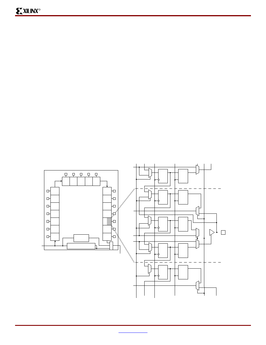
Architectural Description
Virtex Array
The Virtex user-programmable gate array, shown in
Figure 1
, comprises two major configurable elements: con-
figurable logic blocks (CLBs) and input/output blocks
(IOBs).
∑
CLBs provide the functional elements for constructing
logic
∑
IOBs provide the interface between the package pins
and the CLBs
CLBs interconnect through a general routing matrix (GRM).
The GRM comprises an array of routing switches located at
the intersections of horizontal and vertical routing channels.
Each CLB nests into a VersaBlockTM that also provides local
routing resources to connect the CLB to the GRM.
The VersaRingTM I/O interface provides additional routing
resources around the periphery of the device. This routing
improves I/O routability and facilitates pin locking.
The Virtex architecture also includes the following circuits
that connect to the GRM.
∑
Dedicated block memories of 4096 bits each
∑
Clock DLLs for clock-distribution delay compensation
and clock domain control
∑
3-State buffers (BUFTs) associated with each CLB that
drive dedicated segmentable horizontal routing
resources
Values stored in static memory cells control the configurable
logic elements and interconnect resources. These values
load into the memory cells on power-up, and can reload if
necessary to change the function of the device.
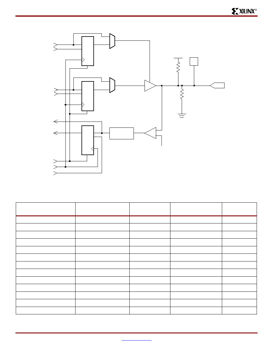
Input/Output Block
The Virtex IOB,
Figure 2
, features SelectIOTM inputs and
outputs that support a wide variety of I/O signalling stan-
dards, see
Table 1
.
The three IOB storage elements function either as edge-trig-
gered D-type flip-flops or as level sensitive latches. Each
IOB has a clock signal (CLK) shared by the three flip-flops
and independent clock enable signals for each flip-flop.
In addition to the CLK and CE control signals, the three
flip-flops share a Set/Reset (SR). For each flip-flop, this sig-
nal can be independently configured as a synchronous Set,
a synchronous Reset, an asynchronous Preset, or an asyn-
chronous Clear.
The output buffer and all of the IOB control signals have
independent polarity controls.
All pads are protected against damage from electrostatic
discharge (ESD) and from over-voltage transients. Two
forms of over-voltage protection are provided, one that per-
mits 5 V compliance, and one that does not. For 5 V compli-
ance, a Zener-like structure connected to ground turns on
when the output rises to approximately 6.5 V. When PCI
3.3 V compliance is required, a conventional clamp diode is
connected to the output supply voltage, V
CCO
.
Optional pull-up and pull-down resistors and an optional
weak-keeper circuit are attached to each pad. Prior to con-
figuration, all pins not involved in configuration are forced
into their high-impedance state. The pull-down resistors and
the weak-keeper circuits are inactive, but inputs can option-
ally be pulled up.
The activation of pull-up resistors prior to configuration is
controlled on a global basis by the configuration mode pins.
If the pull-up resistors are not activated, all the pins will float.
Consequently, external pull-up or pull-down resistors must
be provided on pins required to be at a well-defined logic
level prior to configuration.
All Virtex IOBs support IEEE 1149.1-compatible boundary
scan testing.
0
VirtexTM 2.5 V
Field Programmable Gate Arrays
DS003-2 (v2.8.1) December 9, 2002
0
0
Product Specification
R
Figure 1: Virtex Architecture Overview
vao_b.eps
IOBs
IOBs
IOBs
IOBs
DLL
DLL
DLL
DLL
VersaRing
V
e
r
saRing
VersaRing
V
e
r
saRing
CLBs
BRAMs
BRAMs
VirtexTM 2.5 V Field Programmable Gate Arrays
R
Module 2 of 4
www.xilinx.com
DS003-2 (v2.8.1) December 9, 2002
2
1-800-255-7778
Product Specification
Figure 2: Virtex Input/Output Block (IOB)
OBUFT
IBUF
Vref
ds022_02_091300
SR
CLK
ICE
OCE
O
I
IQ
T
TCE
D
CE
Q
SR
D
CE
Q
SR
D
CE
Q
SR
PAD
Programmable
Delay
Weak
Keeper
Table 1: Supported Select I/O Standards
I/O Standard
Input Reference
Voltage (V
REF
)
Output Source
Voltage (V
CCO
)
Board Termination
Voltage (V
TT
)
5 V Tolerant
LVTTL 2 ≠ 24 mA
N/A
3.3
N/A
Yes
LVCMOS2
N/A
2.5
N/A
Yes
PCI, 5 V
N/A
3.3
N/A
Yes
PCI, 3.3 V
N/A
3.3
N/A
No
GTL
0.8
N/A
1.2
No
GTL+
1.0
N/A
1.5
No
HSTL Class I
0.75
1.5
0.75
No
HSTL Class III
0.9
1.5
1.5
No
HSTL Class IV
0.9
1.5
1.5
No
SSTL3 Class I &II
1.5
3.3
1.5
No
SSTL2 Class I & II
1.25
2.5
1.25
No
CTT
1.5
3.3
1.5
No
AGP
1.32
3.3
N/A
No
VirtexTM 2.5 V Field Programmable Gate Arrays
R
DS003-2 (v2.8.1) December 9, 2002
www.xilinx.com
Module 2 of 4
Product Specification
1-800-255-7778
3
Input Path
A buffer In the Virtex IOB input path routes the input signal
either directly to internal logic or through an optional input
flip-flop.
An optional delay element at the D-input of this flip-flop elim-
inates pad-to-pad hold time. The delay is matched to the
internal clock-distribution delay of the FPGA, and when
used, assures that the pad-to-pad hold time is zero.
Each input buffer can be configured to conform to any of the
low-voltage signalling standards supported. In some of
these standards the input buffer utilizes a user-supplied
threshold voltage, V
REF
. The need to supply V
REF
imposes
constraints on which standards can used in close proximity
to each other. See I/O Banking
, page 3
.
There are optional pull-up and pull-down resistors at each
user I/O input for use after configuration. Their value is in
the range 50 k
≠ 100 k.
Output Path
The output path includes a 3-state output buffer that drives
the output signal onto the pad. The output signal can be
routed to the buffer directly from the internal logic or through
an optional IOB output flip-flop.
The 3-state control of the output can also be routed directly
from the internal logic or through a flip-flip that provides syn-
chronous enable and disable.
Each output driver can be individually programmed for a
wide range of low-voltage signalling standards. Each output
buffer can source up to 24 mA and sink up to 48mA. Drive
strength and slew rate controls minimize bus transients.
In most signalling standards, the output High voltage
depends on an externally supplied V
CCO
voltage. The need
to supply V
CCO
imposes constraints on which standards
can be used in close proximity to each other. See I/O Bank-
ing
, page 3
.
An optional weak-keeper circuit is connected to each out-
put. When selected, the circuit monitors the voltage on the
pad and weakly drives the pin High or Low to match the
input signal. If the pin is connected to a multiple-source sig-
nal, the weak keeper holds the signal in its last state if all
drivers are disabled. Maintaining a valid logic level in this
way eliminates bus chatter.
Because the weak-keeper circuit uses the IOB input buffer
to monitor the input level, an appropriate V
REF
voltage must
be provided if the signalling standard requires one. The pro-
vision of this voltage must comply with the I/O banking
rules.
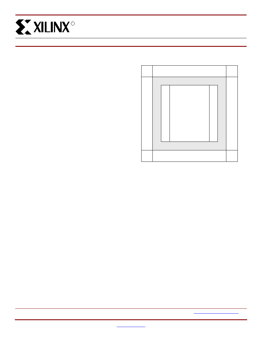
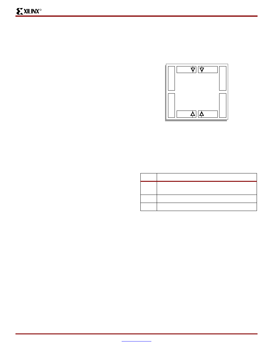
I/O Banking
Some of the I/O standards described above require V
CCO
and/or V
REF
voltages. These voltages externally and con-
nected to device pins that serve groups of IOBs, called
banks. Consequently, restrictions exist about which I/O
standards can be combined within a given bank.
Eight I/O banks result from separating each edge of the
FPGA into two banks, as shown in
Figure 3
. Each bank has
multiple V
CCO
pins, all of which must be connected to the
same voltage. This voltage is determined by the output
standards in use.
Within a bank, output standards can be mixed only if they
use the same V
CCO
. Compatible standards are shown in
Table 2
. GTL and GTL+ appear under all voltages because
their open-drain outputs do not depend on V
CCO
.
Some input standards require a user-supplied threshold
voltage, V
REF
. In this case, certain user-I/O pins are auto-
matically configured as inputs for the V
REF
voltage. Approx-
imately one in six of the I/O pins in the bank assume this
role.
The V
REF
pins within a bank are interconnected internally
and consequently only one V
REF
voltage can be used within
each bank. All V
REF
pins in the bank, however, must be con-
nected to the external voltage source for correct operation.
Within a bank, inputs that require V
REF
can be mixed with
those that do not. However, only one V
REF
voltage can be
used within a bank. Input buffers that use V
REF
are not 5 V
tolerant. LVTTL, LVCMOS2, and PCI 33 MHz 5 V, are 5 V
tolerant.
The V
CCO
and V
REF
pins for each bank appear in the device
Pinout tables and diagrams. The diagrams also show the
bank affiliation of each I/O.
Within a given package, the number of V
REF
and V
CCO
pins
can vary depending on the size of device. In larger devices,
Figure 3:
Virtex I/O Banks
Table 2: Compatible Output Standards
V
CCO
Compatible Standards
3.3 V
PCI, LVTTL, SSTL3 I, SSTL3 II, CTT, AGP, GTL,
GTL+
2.5 V
SSTL2 I, SSTL2 II, LVCMOS2, GTL, GTL+
1.5 V
HSTL I, HSTL III, HSTL IV, GTL, GTL+
X8778_b
Bank 0
GCLK3 GCLK2
GCLK1 GCLK0
Bank 1
Bank 5
Bank 4
Virtex
Device
Bank 7
Bank 6
Bank 2
Bank 3

VirtexTM 2.5 V Field Programmable Gate Arrays
R
Module 2 of 4
www.xilinx.com
DS003-2 (v2.8.1) December 9, 2002
4
1-800-255-7778
Product Specification
more I/O pins convert to V
REF
pins. Since these are always
a superset of the V
REF
pins used for smaller devices, it is
possible to design a PCB that permits migration to a larger
device if necessary. All the V
REF
pins for the largest device
anticipated must be connected to the V
REF
voltage, and not
used for I/O.
In smaller devices, some V
CCO
pins used in larger devices
do not connect within the package. These unconnected pins
can be left unconnected externally, or can be connected to
the V
CCO
voltage to permit migration to a larger device if
necessary.
In TQ144 and PQ/HQ240 packages, all V
CCO
pins are
bonded together internally, and consequently the same
V
CCO
voltage must be connected to all of them. In the
CS144 package, bank pairs that share a side are intercon-
nected internally, permitting four choices for V
CCO
. In both
cases, the V
REF
pins remain internally connected as eight
banks, and can be used as described previously.
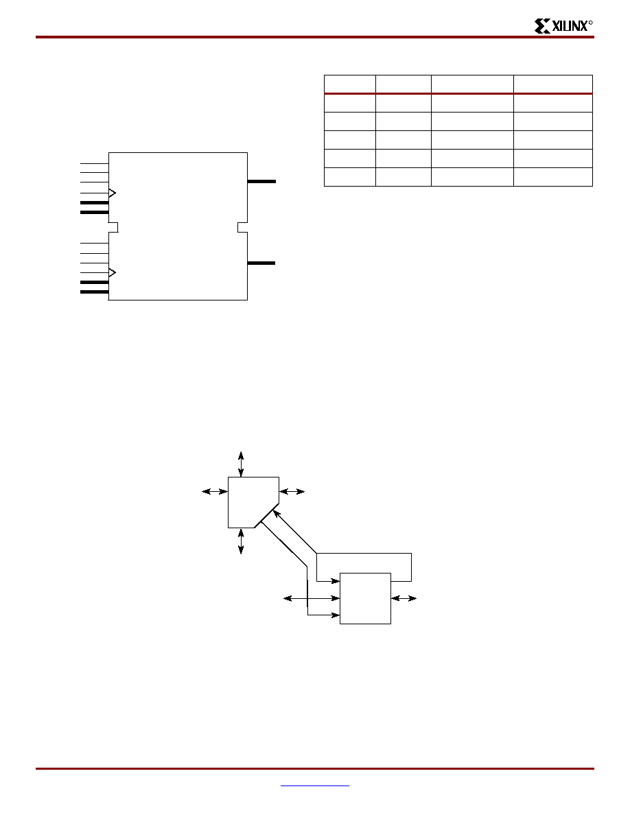
Configurable Logic Block
The basic building block of the Virtex CLB is the logic cell
(LC). An LC includes a 4-input function generator, carry
logic, and a storage element. The output from the function
generator in each LC drives both the CLB output and the D
input of the flip-flop. Each Virtex CLB contains four LCs,
organized in two similar slices, as shown in
Figure 4
.
Figure 5
shows a more detailed view of a single slice.
In addition to the four basic LCs, the Virtex CLB contains
logic that combines function generators to provide functions
of five or six inputs. Consequently, when estimating the
number of system gates provided by a given device, each
CLB counts as 4.5 LCs.
Look-Up Tables
Virtex function generators are implemented as 4-input
look-up tables (LUTs). In addition to operating as a function
generator, each LUT can provide a 16 x 1-bit synchronous
RAM. Furthermore, the two LUTs within a slice can be com-
bined to create a 16 x 2-bit or 32 x 1-bit synchronous RAM,
or a 16x1-bit dual-port synchronous RAM.
The Virtex LUT can also provide a 16-bit shift register that is
ideal for capturing high-speed or burst-mode data. This
mode can also be used to store data in applications such as
Digital Signal Processing.
Storage Elements
The storage elements in the Virtex slice can be configured
either as edge-triggered D-type flip-flops or as level-sensi-
tive latches. The D inputs can be driven either by the func-
tion generators within the slice or directly from slice inputs,
bypassing the function generators.
In addition to Clock and Clock Enable signals, each Slice
has synchronous set and reset signals (SR and BY). SR
forces a storage element into the initialization state speci-
fied for it in the configuration. BY forces it into the opposite
state. Alternatively, these signals can be configured to oper-
ate asynchronously. All of the control signals are indepen-
dently invertible, and are shared by the two flip-flops within
the slice.
Figure 4: 2-Slice Virtex CLB
F1
F2
F3
F4
G1
G2
G3
G4
Carry &
Control
Carry &
Control
Carry &
Control
Carry &
Control
LUT
CIN
CIN
COUT
COUT
YQ
XQ
XQ
YQ
X
XB
Y
YB
YB
Y
BX
BY
BX
BY
G1
G2
G3
G4
F1
F2
F3
F4
slice_b.eps
Slice 1
Slice 0
XB
X
LUT
LUT
LUT
D
EC
Q
RC
SP
D
EC
Q
RC
SP
D
EC
Q
RC
SP
D
EC
Q
RC
SP

VirtexTM 2.5 V Field Programmable Gate Arrays
R
DS003-2 (v2.8.1) December 9, 2002
www.xilinx.com
Module 2 of 4
Product Specification
1-800-255-7778
5
Additional Logic
The F5 multiplexer in each slice combines the function gen-
erator outputs. This combination provides either a function
generator that can implement any 5-input function, a 4:1
multiplexer, or selected functions of up to nine inputs.
Similarly, the F6 multiplexer combines the outputs of all four
function generators in the CLB by selecting one of the
F5-multiplexer outputs. This permits the implementation of
any 6-input function, an 8:1 multiplexer, or selected func-
tions of up to 19 inputs.
Each CLB has four direct feedthrough paths, one per LC.
These paths provide extra data input lines or additional local
routing that does not consume logic resources.
Arithmetic Logic
Dedicated carry logic provides fast arithmetic carry capabil-
ity for high-speed arithmetic functions. The Virtex CLB sup-
ports two separate carry chains, one per Slice. The height
of the carry chains is two bits per CLB.
The arithmetic logic includes an XOR gate that allows a
1-bit full adder to be implemented within an LC. In addition,
a dedicated AND gate improves the efficiency of multiplier
implementation.
The dedicated carry path can also be used to cascade func-
tion generators for implementing wide logic functions.
BUFTs
Each Virtex CLB contains two 3-state drivers (BUFTs) that
can drive on-chip busses. See Dedicated Routing
, page 7
.
Each Virtex BUFT has an independent 3-state control pin
and an independent input pin.
Block SelectRAM
Virtex FPGAs incorporate several large block SelectRAM
memories. These complement the distributed LUT
SelectRAMs that provide shallow RAM structures imple-
mented in CLBs.
Block SelectRAM memory blocks are organized in columns.
All Virtex devices contain two such columns, one along
each vertical edge. These columns extend the full height of
the chip. Each memory block is four CLBs high, and conse-
quently, a Virtex device 64 CLBs high contains 16 memory
blocks per column, and a total of 32 blocks.
Table 3
shows the amount of block SelectRAM memory that
is available in each Virtex device.
Figure 5: Detailed View of VIrtex Slice
BY
F5IN
SR
CLK
CE
BX
YB
Y
YQ
XB
X
XQ
G4
G3
G2
G1
F4
F3
F2
F1
CIN
0
1
1
0
F5
F5
viewslc4.eps
COUT
CY
D
EC
Q
D
EC
Q
F6
CK
WSO
WSH
WE
A4
BY DG
BX
DI
DI
O
WE
I3
I2
I1
I0
LUT
CY
I3
I2
I1
I0
O
DI
WE
LUT
INIT
INIT
REV
REV
Table 3: Virtex Block SelectRAM Amounts
Device
# of Blocks
Total Block SelectRAM Bits
XCV50
8
32,768
XCV100
10
40,960
XCV150
12
49,152
XCV200
14
57,344
XCV300
16
65,536
XCV400
20
81,920
XCV600
24
98,304
XCV800
28
114,688
XCV1000
32
131,072
VirtexTM 2.5 V Field Programmable Gate Arrays
R
Module 2 of 4
www.xilinx.com
DS003-2 (v2.8.1) December 9, 2002
6
1-800-255-7778
Product Specification
Each block SelectRAM cell, as illustrated in
Figure 6
, is a
fully synchronous dual-ported 4096-bit RAM with indepen-
dent control signals for each port. The data widths of the
two ports can be configured independently, providing
built-in bus-width conversion.
Table 4
shows the depth and width aspect ratios for the
block SelectRAM.
The Virtex block SelectRAM also includes dedicated routing
to provide an efficient interface with both CLBs and other
block SelectRAMs. Refer to XAPP130 for block SelectRAM
timing waveforms.
Programmable Routing Matrix
It is the longest delay path that limits the speed of any
worst-case design. Consequently, the Virtex routing archi-
tecture and its place-and-route software were defined in a
single optimization process. This joint optimization mini-
mizes long-path delays, and consequently, yields the best
system performance.
The joint optimization also reduces design compilation
times because the architecture is software-friendly. Design
cycles are correspondingly reduced due to shorter design
iteration times.
Local Routing
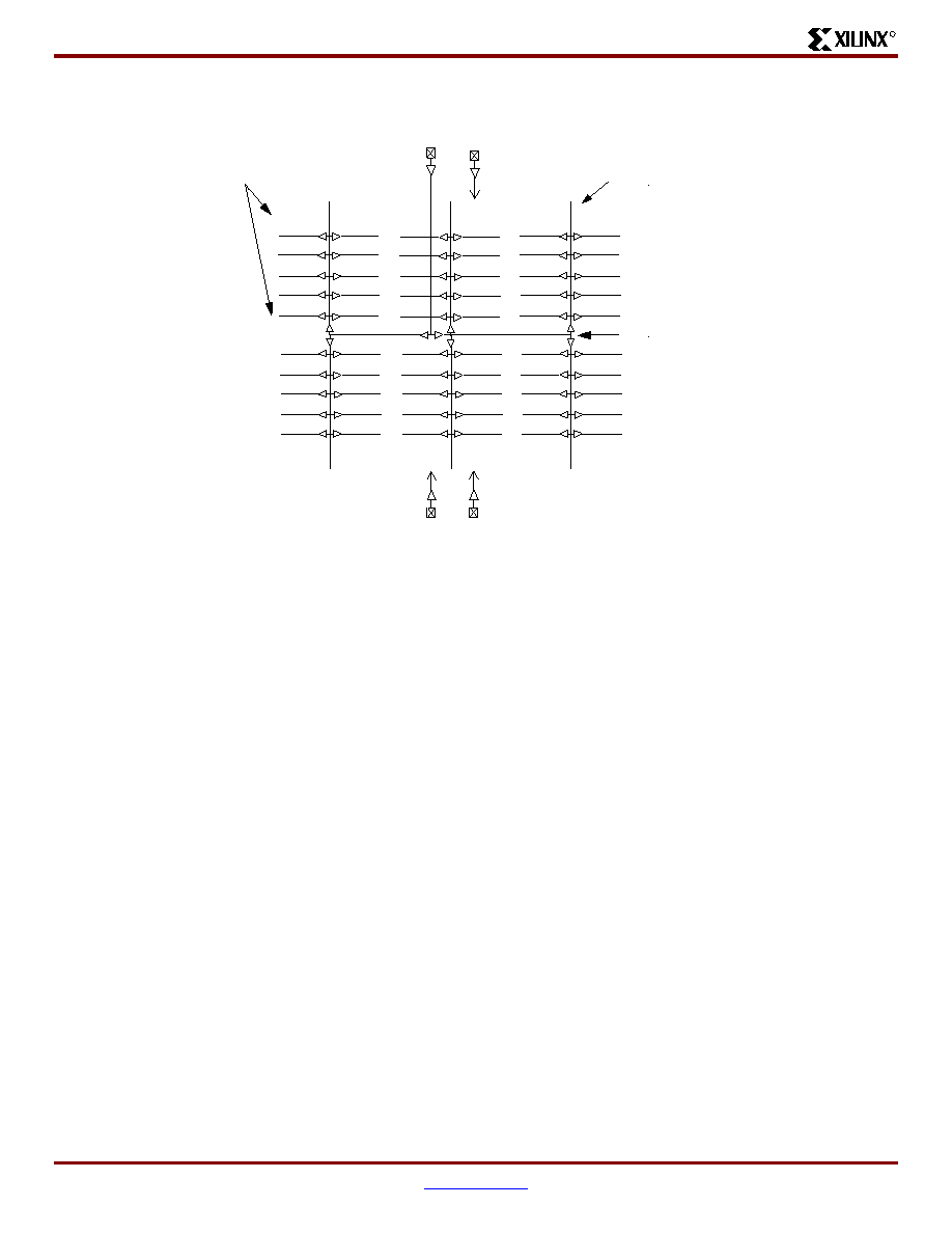
The VersaBlock provides local routing resources, as shown
in
Figure 7
, providing the following three types of connec-
tions.
∑
Interconnections among the LUTs, flip-flops, and GRM
∑
Internal CLB feedback paths that provide high-speed
connections to LUTs within the same CLB, chaining
them together with minimal routing delay
∑
Direct paths that provide high-speed connections
between horizontally adjacent CLBs, eliminating the
delay of the GRM.
Figure 6: Dual-Port Block SelectRAM
WEB
ENB
RSTB
CLKB
ADDRB[#:0]
DIB[#:0]
WEA
ENA
RSTA
CLKA
ADDRA[#:0]
DIA[#:0]
DOA[#:0]
DOB[#:0]
RAMB4_S#_S#
xcv_ds_006
Table 4: Block SelectRAM Port Aspect Ratios
Width
Depth
ADDR Bus
Data Bus
1
4096
ADDR<11:0>
DATA<0>
2
2048
ADDR<10:0>
DATA<1:0>
4
1024
ADDR<9:0>
DATA<3:0>
8
512
ADDR<8:0>
DATA<7:0>
16
256
ADDR<7:0>
DATA<15:0>
Figure 7: Virtex Local Routing
X8794b
CLB
GRM
To Adjacent
GRM
To Adjacent
GRM
Direct Connection
To Adjacent
CLB
To Adjacent
GRM
To Adjacent
GRM
Direct Connection
To Adjacent
CLB
VirtexTM 2.5 V Field Programmable Gate Arrays
R
DS003-2 (v2.8.1) December 9, 2002
www.xilinx.com
Module 2 of 4
Product Specification
1-800-255-7778
7
General Purpose Routing
Most Virtex signals are routed on the general purpose rout-
ing, and consequently, the majority of interconnect
resources are associated with this level of the routing hier-
archy. The general routing resources are located in horizon-
tal and vertical routing channels associated with the rows
and columns CLBs. The general-purpose routing resources
are listed below.
∑
Adjacent to each CLB is a General Routing Matrix
(GRM). The GRM is the switch matrix through which
horizontal and vertical routing resources connect, and
is also the means by which the CLB gains access to
the general purpose routing.
∑
24 single-length lines route GRM signals to adjacent
GRMs in each of the four directions.
∑
12 buffered Hex lines route GRM signals to another
GRMs six-blocks away in each one of the four
directions. Organized in a staggered pattern, Hex lines
can be driven only at their endpoints. Hex-line signals
can be accessed either at the endpoints or at the
midpoint (three blocks from the source). One third of
the Hex lines are bidirectional, while the remaining
ones are uni-directional.
∑
12 Longlines are buffered, bidirectional wires that
distribute signals across the device quickly and
efficiently. Vertical Longlines span the full height of the
device, and horizontal ones span the full width of the
device.
I/O Routing
Virtex devices have additional routing resources around
their periphery that form an interface between the CLB array
and the IOBs. This additional routing, called the VersaRing,
facilitates pin-swapping and pin-locking, such that logic
redesigns can adapt to existing PCB layouts. Time-to-mar-
ket is reduced, since PCBs and other system components
can be manufactured while the logic design is still in
progress.
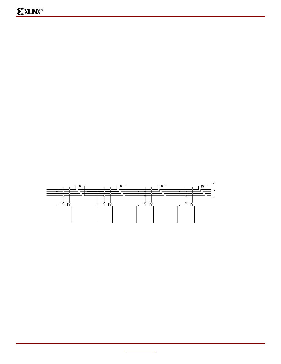
Dedicated Routing
Some classes of signal require dedicated routing resources
to maximize performance. In the Virtex architecture, dedi-
cated routing resources are provided for two classes of sig-
nal.
∑
Horizontal routing resources are provided for on-chip
3-state busses. Four partitionable bus lines are
provided per CLB row, permitting multiple busses
within a row, as shown in
Figure 8
.
∑
Two dedicated nets per CLB propagate carry signals
vertically to the adjacent CLB.
Global Routing
Global Routing resources distribute clocks and other sig-
nals with very high fanout throughout the device. Virtex
devices include two tiers of global routing resources
referred to as primary global and secondary local clock rout-
ing resources.
∑
The primary global routing resources are four
dedicated global nets with dedicated input pins that are
designed to distribute high-fanout clock signals with
minimal skew. Each global clock net can drive all CLB,
IOB, and block RAM clock pins. The primary global
nets can only be driven by global buffers. There are
four global buffers, one for each global net.
∑
The secondary local clock routing resources consist of
24 backbone lines, 12 across the top of the chip and 12
across bottom. From these lines, up to 12 unique
signals per column can be distributed via the 12
longlines in the column. These secondary resources
are more flexible than the primary resources since they
are not restricted to routing only to clock pins.
Clock Distribution
Virtex provides high-speed, low-skew clock distribution
through the primary global routing resources described
above. A typical clock distribution net is shown in
Figure 9
.
Four global buffers are provided, two at the top center of the
device and two at the bottom center. These drive the four
primary global nets that in turn drive any clock pin.
Figure 8: BUFT Connections to Dedicated Horizontal Bus Lines
CLB
CLB
CLB
CLB
buft_c.eps
Tri-State
Lines
VirtexTM 2.5 V Field Programmable Gate Arrays
R
Module 2 of 4
www.xilinx.com
DS003-2 (v2.8.1) December 9, 2002
8
1-800-255-7778
Product Specification
Four dedicated clock pads are provided, one adjacent to
each of the global buffers. The input to the global buffer is
selected either from these pads or from signals in the gen-
eral purpose routing.
Delay-Locked Loop (DLL)
Associated with each global clock input buffer is a fully digi-
tal Delay-Locked Loop (DLL) that can eliminate skew
between the clock input pad and internal clock-input pins
throughout the device. Each DLL can drive two global clock
networks.The DLL monitors the input clock and the distrib-
uted clock, and automatically adjusts a clock delay element.
Clock edges reach internal flip-flops one to four clock peri-
ods after they arrive at the input. This closed-loop system
effectively eliminates clock-distribution delay by ensuring
that clock edges arrive at internal flip-flops in synchronism
with clock edges arriving at the input.
In addition to eliminating clock-distribution delay, the DLL
provides advanced control of multiple clock domains. The
DLL provides four quadrature phases of the source clock,
can double the clock, or divide the clock by 1.5, 2, 2.5, 3, 4,
5, 8, or 16.
The DLL also operates as a clock mirror. By driving the out-
put from a DLL off-chip and then back on again, the DLL can
be used to de-skew a board level clock among multiple Vir-
tex devices.
In order to guarantee that the system clock is operating cor-
rectly prior to the FPGA starting up after configuration, the
DLL can delay the completion of the configuration process
until after it has achieved lock.
See DLL Timing Parameters
, page 21
of Module 3, for fre-
quency range information.
Boundary Scan
Virtex devices support all the mandatory boundary-scan
instructions specified in the IEEE standard 1149.1. A Test
Access Port (TAP) and registers are provided that implement
the EXTEST, INTEST, SAMPLE/PRELOAD, BYPASS,
IDCODE, USERCODE, and HIGHZ instructions. The TAP
also supports two internal scan chains and configura-
tion/readback of the device.The TAP uses dedicated package
pins that always operate using LVTTL. For TDO to operate
using LVTTL, the V
CCO
for Bank 2 should be 3.3 V. Other-
wise, TDO switches rail-to-rail between ground and V
CCO
.
Boundary-scan operation is independent of individual IOB
configurations, and unaffected by package type. All IOBs,
including un-bonded ones, are treated as independent
3-state bidirectional pins in a single scan chain. Retention of
the bidirectional test capability after configuration facilitates
the testing of external interconnections, provided the user
design or application is turned off.
Table 5
lists the boundary-scan instructions supported in
Virtex FPGAs. Internal signals can be captured during
EXTEST by connecting them to un-bonded or unused IOBs.
They can also be connected to the unused outputs of IOBs
defined as unidirectional input pins.
Before the device is configured, all instructions except
USER1 and USER2 are available. After configuration, all
instructions are available. During configuration, it is recom-
mended that those operations using the boundary-scan
register (SAMPLE/PRELOAD, INTEST, EXTEST) not be
performed.
Figure 9: Global Clock Distribution Network
Global Clock Spine
Global Clock Column
GCLKPAD2
GCLKBUF2
GCLKPAD3
GCLKBUF3
GCLKBUF1
GCLKPAD1
GCLKBUF0
GCLKPAD0
Global Clock Rows
gclkbu_2.eps
VirtexTM 2.5 V Field Programmable Gate Arrays
R
DS003-2 (v2.8.1) December 9, 2002
www.xilinx.com
Module 2 of 4
Product Specification
1-800-255-7778
9
In addition to the test instructions outlined above, the
boundary-scan circuitry can be used to configure the
FPGA, and also to read back the configuration data.
Figure 10
is a diagram of the Virtex Series boundary scan
logic. It includes three bits of Data Register per IOB, the
IEEE 1149.1 Test Access Port controller, and the Instruction
Register with decodes.
Instruction Set
The Virtex Series boundary scan instruction set also
includes instructions to configure the device and read back
configuration data (CFG_IN, CFG_OUT, and JSTART). The
complete instruction set is coded as shown in
Table 5
.
Data Registers
The primary data register is the boundary scan register. For
each IOB pin in the FPGA, bonded or not, it includes three
bits for In, Out, and 3-State Control. Non-IOB pins have
appropriate partial bit population if input-only or output-only.
Each EXTEST CAPTURED-OR state captures all In, Out,
and 3-state pins.
The other standard data register is the single flip-flop
BYPASS register. It synchronizes data being passed
through the FPGA to the next downstream boundary scan
device.
The FPGA supports up to two additional internal scan
chains that can be specified using the BSCAN macro. The
macro provides two user pins (SEL1 and SEL2) which are
decodes of the USER1 and USER2 instructions respec-
tively. For these instructions, two corresponding pins (TDO1
and TDO2) allow user scan data to be shifted out of TDO.
Likewise, there are individual clock pins (DRCK1 and
DRCK2) for each user register. There is a common input pin
(TDI) and shared output pins that represent the state of the
TAP controller (RESET, SHIFT, and UPDATE).
Bit Sequence
The order within each IOB is: In, Out, 3-State. The
input-only pins contribute only the In bit to the boundary
scan I/O data register, while the output-only pins contributes
all three bits.
From a cavity-up view of the chip (as shown in EPIC), start-
ing in the upper right chip corner, the boundary scan
data-register bits are ordered as shown in
Figure 11
.
BSDL (Boundary Scan Description Language) files for Vir-
tex Series devices are available on the Xilinx web site in the
File Download area.
Figure 10: Virtex Series Boundary Scan Logic
D
Q
D
Q
IOB
IOB
IOB
IOB
IOB
IOB
IOB
IOB
IOB
IOB
IOB
IOB
IOB
M
U
X
BYPASS
REGISTER
IOB
IOB
TDO
TDI
IOB
IOB
IOB
1
0
1
0
1
0
1
0
1
0
sd
LE
D
Q
D
Q
D
Q
1
0
1
0
1
0
1
0
D
Q
LE
sd
sd
LE
D
Q
sd
LE
D
Q
IOB
D
Q
1
0
D
Q
LE
sd
IOB.T
DATA IN
IOB.I
IOB.Q
IOB.T
IOB.I
SHIFT/
CAPTURE
CLOCK DATA
REGISTER
DATAOUT
UPDATE
EXTEST
X9016
INSTRUCTION REGISTER

VirtexTM 2.5 V Field Programmable Gate Arrays
R
Module 2 of 4
www.xilinx.com
DS003-2 (v2.8.1) December 9, 2002
10
1-800-255-7778
Product Specification
Identification Registers
The IDCODE register is supported. By using the IDCODE,
the device connected to the JTAG port can be determined.
The IDCODE register has the following binary format:
vvvv:ffff:fffa:aaaa:aaaa:cccc:cccc:ccc1
where
v = the die version number
f = the family code (03h for Virtex family)
a = the number of CLB rows (ranges from 010h for XCV50
to 040h for XCV1000)
c = the company code (49h for Xilinx)
The USERCODE register is supported. By using the USER-
CODE, a user-programmable identification code can be
loaded and shifted out for examination. The identification
code is embedded in the bitstream during bitstream gener-
ation and is valid only after configuration.
Including Boundary Scan in a Design
Since the boundary scan pins are dedicated, no special ele-
ment needs to be added to the design unless an internal
data register (USER1 or USER2) is desired.
If an internal data register is used, insert the boundary scan
symbol and connect the necessary pins as appropriate.
Development System
Virtex FPGAs are supported by the Xilinx Foundation and
Alliance CAE tools. The basic methodology for Virtex design
consists of three interrelated steps: design entry, imple-
mentation, and verification. Industry-standard tools are
used for design entry and simulation (for example, Synop-
sys FPGA Express), while Xilinx provides proprietary archi-
tecture-specific tools for implementation.
The Xilinx development system is integrated under the Xil-
inx Design Manager (XDMTM) software, providing designers
Figure 11: Boundary Scan Bit Sequence
Table 5: Boundary Scan Instructions
Boundary-Scan
Command
Binary
Code(4:0)
Description
EXTEST
00000
Enables boundary-scan
EXTEST operation
SAMPLE/PRELOAD
00001
Enables boundary-scan
SAMPLE/PRELOAD
operation
USER 1
00010
Access user-defined
register 1
USER 2
00011
Access user-defined
register 2
CFG_OUT
00100
Access the configuration
bus for read operations.
CFG_IN
00101
Access the configuration
bus for write operations.
INTEST
00111
Enables boundary-scan
INTEST operation
USERCODE
01000
Enables shifting out
USER code
IDCODE
01001
Enables shifting out of ID
Code
HIGHZ
01010
3-states output pins while
enabling the Bypass
Register
JSTART
01100
Clock the start-up
sequence when
StartupClk is TCK
BYPASS
11111
Enables BYPASS
RESERVED
All other
codes
Xilinx reserved
instructions
Bit 0 ( TDO end)
Bit 1
Bit 2
Right half of Top-edge IOBs (Right-to-Left)
GCLK2
GCLK3
Left half of Top-edge IOBs (Right-to-Left)
Left-edge IOBs (Top-to-Bottom)
M1
M0
M2
Left half of Bottom-edge IOBs (Left-to-Right)
GCLK1
GCLK0
Right half of Bottom-edge IOBs (Left-to-Right)
DONE
PROG
Right-edge IOBs (Bottom -to-Top)
CCLK
(TDI end)
990602001
Table 6: IDCODEs Assigned to Virtex FPGAs
FPGA
IDCODE
XCV50
v0610093h
XCV100
v0614093h
XCV150
v0618093h
XCV200
v061C093h
XCV300
v0620093h
XCV400
v0628093h
XCV600
v0630093h
XCV800
v0638093h
XCV1000
v0640093h

VirtexTM 2.5 V Field Programmable Gate Arrays
R
DS003-2 (v2.8.1) December 9, 2002
www.xilinx.com
Module 2 of 4
Product Specification
1-800-255-7778
11
with a common user interface regardless of their choice of
entry and verification tools. The XDM software simplifies the
selection of implementation options with pull-down menus
and on-line help.
Application programs ranging from schematic capture to
Placement and Routing (PAR) can be accessed through the
XDM software. The program command sequence is gener-
ated prior to execution, and stored for documentation.
Several advanced software features facilitate Virtex design.
RPMs, for example, are schematic-based macros with rela-
tive location constraints to guide their placement. They help
ensure optimal implementation of common functions.
For HDL design entry, the Xilinx FPGA Foundation develop-
ment system provides interfaces to the following synthesis
design environments.
∑
Synopsys (FPGA Compiler, FPGA Express)
∑
Exemplar (Spectrum)
∑
Synplicity (Synplify)
For schematic design entry, the Xilinx FPGA Foundation
and alliance development system provides interfaces to the
following schematic-capture design environments.
∑
Mentor Graphics V8 (Design Architect, QuickSim II)
∑
Viewlogic Systems (Viewdraw)
Third-party vendors support many other environments.
A standard interface-file specification, Electronic Design
Interchange Format (EDIF), simplifies file transfers into and
out of the development system.
Virtex FPGAs supported by a unified library of standard
functions. This library contains over 400 primitives and mac-
ros, ranging from 2-input AND gates to 16-bit accumulators,
and includes arithmetic functions, comparators, counters,
data registers, decoders, encoders, I/O functions, latches,
Boolean functions, multiplexers, shift registers, and barrel
shifters.
The "soft macro" portion of the library contains detailed
descriptions of common logic functions, but does not con-
tain any partitioning or placement information. The perfor-
mance of these macros depends, therefore, on the
partitioning and placement obtained during implementation.
RPMs, on the other hand, do contain predetermined parti-
tioning and placement information that permits optimal
implementation of these functions. Users can create their
own library of soft macros or RPMs based on the macros
and primitives in the standard library.
The design environment supports hierarchical design entry,
with high-level schematics that comprise major functional
blocks, while lower-level schematics define the logic in
these blocks. These hierarchical design elements are auto-
matically combined by the implementation tools. Different
design entry tools can be combined within a hierarchical
design, thus allowing the most convenient entry method to
be used for each portion of the design.
Design Implementation
The place-and-route tools (PAR) automatically provide the
implementation flow described in this section. The parti-
tioner takes the EDIF net list for the design and maps the
logic into the architectural resources of the FPGA (CLBs
and IOBs, for example). The placer then determines the
best locations for these blocks based on their interconnec-
tions and the desired performance. Finally, the router inter-
connects the blocks.
The PAR algorithms support fully automatic implementation
of most designs. For demanding applications, however, the
user can exercise various degrees of control over the pro-
cess. User partitioning, placement, and routing information
is optionally specified during the design-entry process. The
implementation of highly structured designs can benefit
greatly from basic floor planning.
The implementation software incorporates Timing Wizard
Æ
timing-driven placement and routing. Designers specify tim-
ing requirements along entire paths during design entry.
The timing path analysis routines in PAR then recognize
these user-specified requirements and accommodate them.
Timing requirements are entered on a schematic in a form
directly relating to the system requirements, such as the tar-
geted clock frequency, or the maximum allowable delay
between two registers. In this way, the overall performance
of the system along entire signal paths is automatically tai-
lored to user-generated specifications. Specific timing infor-
mation for individual nets is unnecessary.
Design Verification
In addition to conventional software simulation, FPGA users
can use in-circuit debugging techniques. Because Xilinx
devices are infinitely reprogrammable, designs can be veri-
fied in real time without the need for extensive sets of soft-
ware simulation vectors.
The development system supports both software simulation
and in-circuit debugging techniques. For simulation, the
system extracts the post-layout timing information from the
design database, and back-annotates this information into
the net list for use by the simulator. Alternatively, the user
can verify timing-critical portions of the design using the
TRACE
Æ
static timing analyzer.
For in-circuit debugging, the development system includes
a download and readback cable. This cable connects the
FPGA in the target system to a PC or workstation. After
downloading the design into the FPGA, the designer can
single-step the logic, readback the contents of the flip-flops,
and so observe the internal logic state. Simple modifica-
tions can be downloaded into the system in a matter of min-
utes.
VirtexTM 2.5 V Field Programmable Gate Arrays
R
Module 2 of 4
www.xilinx.com
DS003-2 (v2.8.1) December 9, 2002
12
1-800-255-7778
Product Specification
Configuration
Virtex devices are configured by loading configuration data
into the internal configuration memory. Some of the pins
used for this are dedicated configuration pins, while others
can be re-used as general purpose inputs and outputs once
configuration is complete.
The following are dedicated pins:
∑
Mode pins (M2, M1, M0)
∑
Configuration clock pin (CCLK)
∑
PROGRAM pin
∑
DONE pin
∑
Boundary-scan pins (TDI, TDO, TMS, TCK)
Depending on the configuration mode chosen, CCLK can
be an output generated by the FPGA, or it can be generated
externally and provided to the FPGA as an input. The
PROGRAM pin must be pulled High prior to reconfiguration.
Note that some configuration pins can act as outputs. For
correct operation, these pins can require a V
CCO
of 3.3 V to
permit LVTTL operation. All the pins affected are in banks 2
or 3. The configuration pins needed for SelectMap (CS,
Write) are located in bank 1.
After Virtex devices are configured, unused IOBs function
as 3-state OBUFTs with weak pull downs. For a more
detailed description than that given below, see the
XAPP138, Virtex Configuration and Readback.
Configuration Modes
Virtex supports the following four configuration modes.
∑
Slave-serial mode
∑
Master-serial mode
∑
SelectMAP mode
∑
Boundary-scan mode
The Configuration mode pins (M2, M1, M0) select among
these configuration modes with the option in each case of
having the IOB pins either pulled up or left floating prior to
configuration. The selection codes are listed in
Table 7
.
Configuration through the boundary-scan port is always
available, independent of the mode selection. Selecting the
boundary-scan mode simply turns off the other modes. The
three mode pins have internal pull-up resistors, and default
to a logic High if left unconnected. However, it is recom-
mended to drive the configuration mode pins externally.
Slave-Serial Mode
In slave-serial mode, the FPGA receives configuration data
in bit-serial form from a serial PROM or other source of
serial configuration data. The serial bitstream must be setup
at the DIN input pin a short time before each rising edge of
an externally generated CCLK.
For more information on serial PROMs, see the PROM data
sheet at:
http://www.xilinx.com/bvdocs/publications/ds026.pdf
.
Multiple FPGAs can be daisy-chained for configuration from a
single source. After a particular FPGA has been configured,
the data for the next device is routed to the DOUT pin. The
data on the DOUT pin changes on the rising edge of CCLK.
The change of DOUT on the rising edge of CCLK differs
from previous families, but does not cause a problem for
mixed configuration chains. This change was made to
improve serial configuration rates for Virtex-only chains.
Figure 12
shows a full master/slave system. A Virtex device
in slave-serial mode should be connected as shown in the
third device from the left.
Slave-serial mode is selected by applying <111> or <011>
to the mode pins (M2, M1, M0). A weak pull-up on the mode
pins makes slave-serial the default mode if the pins are left
unconnected. However, it is recommended to drive the con-
figuration mode pins externally.
Figure 13
shows
slave-serial mode programming switching characteristics.
Table 8
provides more detail about the characteristics
shown in
Figure 13
. Configuration must be delayed until the
INIT pins of all daisy-chained FPGAs are High.
Table 7: Configuration Codes
Configuration Mode
M2
M1
M0
CCLK Direction
Data Width
Serial D
out
Configuration Pull-ups
Master-serial mode
0
0
0
Out
1
Yes
No
Boundary-scan mode
1
0
1
N/A
1
No
No
SelectMAP mode
1
1
0
In
8
No
No
Slave-serial mode
1
1
1
In
1
Yes
No
Master-serial mode
1
0
0
Out
1
Yes
Yes
Boundary-scan mode
0
0
1
N/A
1
No
Yes
SelectMAP mode
0
1
0
In
8
No
Yes
Slave-serial mode
0
1
1
In
1
Yes
Yes
VirtexTM 2.5 V Field Programmable Gate Arrays
R
DS003-2 (v2.8.1) December 9, 2002
www.xilinx.com
Module 2 of 4
Product Specification
1-800-255-7778
13
Table 8: Master/Slave Serial Mode Programming Switching
Description
Figure
References
Symbol
Values
Units
CCLK
DIN setup/hold, slave mode
1/2
T
DCC
/T
CCD
5.0 / 0
ns, min
DIN setup/hold, master mode
1/2
T
DSCK
/T
CKDS
5.0 / 0
ns, min
DOUT
3
T
CCO
12.0
ns, max
High time
4
T
CCH
5.0
ns, min
Low time
5
T
CCL
5.0
ns, min
Maximum Frequency
F
CC
66
MHz, max
Frequency Tolerance, master mode with
respect to nominal
+45%
≠30%
Figure 12: Master/Slave Serial Mode Circuit Diagram
VIRTEX
MASTER
SERIAL
VIRTEX,
XC4000XL,
SLAVE
XC1701L
PROGRAM
M2
M0 M1
DOUT
CCLK
CLK
DATA
CE
CEO
RESET/OE
DONE
DIN
INIT
INIT
DONE
PROGRAM
PROGRAM
CCLK
DIN
DOUT
M2
M0 M1
(Low Reset Option Used)
4.7 K
xcv_12_091499
3.3V
V
CC
Optional Pull-up
Resistor on Done
Note 1: If none of the Virtex FPGAs have been selected to drive DONE, an external pull-up resistor of 330
should be added to the common DONE line.
1
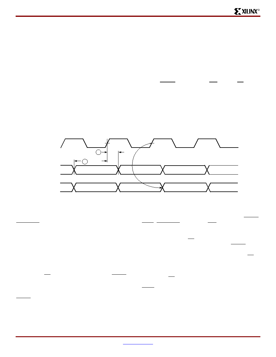
Figure 13: Slave-Serial Mode Programming Switching Characteristics
4 T
CCH
3 T
CCO
5 T
CCL
2 T
CCD
1 T
DCC
DIN
CCLK
DOUT
(Output)
X5379_a
VirtexTM 2.5 V Field Programmable Gate Arrays
R
Module 2 of 4
www.xilinx.com
DS003-2 (v2.8.1) December 9, 2002
14
1-800-255-7778
Product Specification
Master-Serial Mode
In master-serial mode, the CCLK output of the FPGA drives
a Xilinx Serial PROM that feeds bit-serial data to the DIN
input. The FPGA accepts this data on each rising CCLK
edge. After the FPGA has been loaded, the data for the next
device in a daisy-chain is presented on the DOUT pin after
the rising CCLK edge.
The interface is identical to slave-serial except that an inter-
nal oscillator is used to generate the configuration clock
(CCLK). A wide range of frequencies can be selected for
CCLK which always starts at a slow default frequency. Con-
figuration bits then switch CCLK to a higher frequency for
the remainder of the configuration. Switching to a lower fre-
quency is prohibited.
The CCLK frequency is set using the ConfigRate option in
the bitstream generation software. The maximum CCLK fre-
quency that can be selected is 60 MHz. When selecting a
CCLK frequency, ensure that the serial PROM and any
daisy-chained FPGAs are fast enough to support the clock
rate.
On power-up, the CCLK frequency is 2.5 MHz. This fre-
quency is used until the ConfigRate bits have been loaded
when the frequency changes to the selected ConfigRate.
Unless a different frequency is specified in the design, the
default ConfigRate is 4 MHz.
Figure 12
shows a full master/slave system. In this system,
the left-most device operates in master-serial mode. The
remaining devices operate in slave-serial mode. The
SPROM RESET pin is driven by INIT, and the CE input is
driven by DONE. There is the potential for contention on the
DONE pin, depending on the start-up sequence options
chosen.
Figure 14
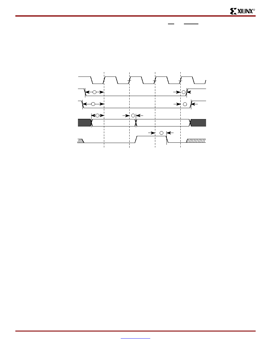
shows the timing of master-serial configuration.
Master-serial mode is selected by a <000> or <100> on the
mode pins (M2, M1, M0).
Table 8
shows the timing informa-
tion for
Figure 14
.
At power-up, V
CC
must rise from 1.0 V to V
CC
min in less
than 50 ms, otherwise delay configuration by pulling
PROGRAM Low until V
CC
is valid.
The sequence of operations necessary to configure a Virtex
FPGA serially appears in
Figure 15
.
SelectMAP Mode
The SelectMAP mode is the fastest configuration option.
Byte-wide data is written into the FPGA with a BUSY flag
controlling the flow of data.
An external data source provides a byte stream, CCLK, a
Chip Select (CS) signal and a Write signal (WRITE). If
BUSY is asserted (High) by the FPGA, the data must be
held until BUSY goes Low.
Data can also be read using the SelectMAP mode. If
WRITE is not asserted, configuration data is read out of the
FPGA as part of a readback operation.
In the SelectMAP mode, multiple Virtex devices can be
chained in parallel. DATA pins (D7:D0), CCLK, WRITE,
BUSY, PROGRAM, DONE, and INIT can be connected in
parallel between all the FPGAs. Note that the data is orga-
nized with the MSB of each byte on pin DO and the LSB of
each byte on D7. The CS pins are kept separate, insuring
that each FPGA can be selected individually. WRITE should
be Low before loading the first bitstream and returned High
after the last device has been programmed. Use CS to
select the appropriate FPGA for loading the bitstream and
sending the configuration data. at the end of the bitstream,
deselect the loaded device and select the next target FPGA
by setting its CS pin High. A free-running oscillator or other
externally generated signal can be used for CCLK. The
BUSY signal can be ignored for frequencies below 50 MHz.
For details about frequencies above 50 MHz, see
XAPP138, Virtex Configuration and Readback. Once all the
devices have been programmed, the DONE pin goes High.
Figure 14: Master-Serial Mode Programming Switching Characteristics
Serial Data In
CCLK
(Output)
Serial DOUT
(Output)
1 TDSCK
2
TCKDS
DS022_44_071201
VirtexTM 2.5 V Field Programmable Gate Arrays
R
DS003-2 (v2.8.1) December 9, 2002
www.xilinx.com
Module 2 of 4
Product Specification
1-800-255-7778
15
After configuration, the pins of the SelectMAP port can be
used as additional user I/O. Alternatively, the port can be
retained to permit high-speed 8-bit readback.
Retention of the SelectMAP port is selectable on a
design-by-design basis when the bitstream is generated. If
retention is selected, PROHIBIT constraints are required to
prevent the SelectMAP-port pins from being used as user
I/O.
Multiple Virtex FPGAs can be configured using the Select-
MAP mode, and be made to start-up simultaneously. To
configure multiple devices in this way, wire the individual
CCLK, Data, WRITE, and BUSY pins of all the devices in
parallel. The individual devices are loaded separately by
asserting the CS pin of each device in turn and writing the
appropriate data.
S
ee
Table 9
for SelectMAP Write Timing
Characteristics.
.
Write
Write operations send packets of configuration data into the
FPGA. The sequence of operations for a multi-cycle write
operation is shown below. Note that a configuration packet
can be split into many such sequences. The packet does
not have to complete within one assertion of CS, illustrated
in
Figure 16
.
1.
Assert WRITE and CS Low. Note that when CS is
asserted on successive CCLKs, WRITE must remain
either asserted or de-asserted. Otherwise an abort will
be initiated, as described below.
2.
Drive data onto D[7:0]. Note that to avoid contention,
the data source should not be enabled while CS is Low
and WRITE is High. Similarly, while WRITE is High, no
more that one CS should be asserted.
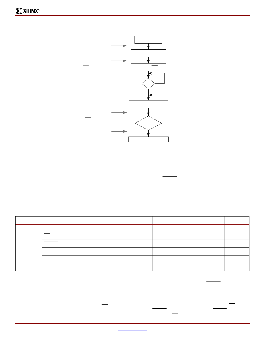
Figure 15: Serial Configuration Flowchart
Apply Power
Set PROGRAM = High
Release INIT
If used to delay
configuration
Load a Configuration Bit
High
Low
FPGA makes a final
clearing pass and releases
INIT when finished.
FPGA starts to clear
configuration memory.
ds003_154_111799
Configuration Completed
End of
Bitstream?
Yes
No
Once per bitstream,
FPGA checks data using CRC
and pulls INIT Low on error.
If no CRC errors found,
FPGA enters start-up phase
causing DONE to go High.
INIT?
Table 9: SelectMAP Write Timing Characteristics
Description
Symbol
Units
CCLK
D
0-7
Setup/Hold 1/2
T
SMDCC
/T
SMCCD
5.0 / 1.7
ns, min
CS Setup/Hold
3/4
T
SMCSCC
/T
SMCCCS
7.0 / 1.7
ns, min
WRITE Setup/Hold
5/6
T
SMCCW
/T
SMWCC
7.0 / 1.7
ns, min
BUSY Propagation Delay
7
T
SMCKBY
12.0
ns, max
Maximum Frequency
F
CC
66
MHz, max
Maximum Frequency with no handshake
F
CCNH
50
MHz, max
VirtexTM 2.5 V Field Programmable Gate Arrays
R
Module 2 of 4
www.xilinx.com
DS003-2 (v2.8.1) December 9, 2002
16
1-800-255-7778
Product Specification
3.
At the rising edge of CCLK: If BUSY is Low, the data is
accepted on this clock. If BUSY is High (from a previous
write), the data is not accepted. Acceptance will instead
occur on the first clock after BUSY goes Low, and the
data must be held until this has happened.
4.
Repeat steps 2 and 3 until all the data has been sent.
5.
De-assert CS and WRITE.
A flowchart for the write operation appears in
Figure 17
.
Note that if CCLK is slower than f
CCNH
, the FPGA never
asserts BUSY. In this case, the above handshake is unnec-
essary, and data can simply be entered into the FPGA every
CCLK cycle.
Figure 16: Write Operations
ds003_16_071902
CCLK
Write
Write
No Write
Write
DATA[0:7]
CS
WRITE
3
5
BUSY
4
6
7
1
2

VirtexTM 2.5 V Field Programmable Gate Arrays
R
DS003-2 (v2.8.1) December 9, 2002
www.xilinx.com
Module 2 of 4
Product Specification
1-800-255-7778
17
Abort
During a given assertion of CS, the user cannot switch from
a write to a read, or vice-versa. This action causes the cur-
rent packet command to be aborted. The device will remain
BUSY until the aborted operation has completed. Following
an abort, data is assumed to be unaligned to word bound-
aries, and the FPGA requires a new synchronization word
prior to accepting any new packets.
To initiate an abort during a write operation, de-assert
WRITE. At the rising edge of CCLK, an abort is initiated, as
shown in
Figure 18
.
Figure 17: SelectMAP Flowchart for Write Operation
Apply Power
Release INIT
If used to delay
configuration
On first FPGA
PROGRAM
from Low
to High
Set WRITE = Low
Enter Data Source
Set CS = Low
On first FPGA
Set CS = High
Apply Configuration Byte
INIT?
High
Low
Yes
No
Busy?
Low
High
Disable Data Source
Set WRITE = High
When all DONE pins
are released, DONE goes High
and start-up sequences complete.
If no errors,
later FPGAs enter start-up phase
releasing DONE.
If no errors,
first FPGAs enter start-up phase
releasing DONE.
Once per bitstream,
FPGA checks data using CRC
and pulls INIT Low on error.
FPGA makes a final
clearing pass and releases
INIT when finished.
FPGA starts to clear
configuration memory.
For any other FPGAs
ds003_17_090602
Repeat Sequence A
Configuration Completed
Sequence A
End of Data?
Yes
No

VirtexTM 2.5 V Field Programmable Gate Arrays
R
Module 2 of 4
www.xilinx.com
DS003-2 (v2.8.1) December 9, 2002
18
1-800-255-7778
Product Specification
Boundary-Scan Mode
In the boundary-scan mode, configuration is done through
the IEEE 1149.1 Test Access Port. Note that the
PROGRAM pin must be pulled High prior to reconfiguration.
A Low on the PROGRAM pin resets the TAP controller and
no JTAG operations can be performed.
Configuration through the TAP uses the CFG_IN instruc-
tion. This instruction allows data input on TDI to be con-
verted into data packets for the internal configuration bus.
The following steps are required to configure the FPGA
through the boundary-scan port (when using TCK as a
start-up clock).
1.
Load the CFG_IN instruction into the boundary-scan
instruction register (IR)
2.
Enter the Shift-DR (SDR) state
3.
Shift a configuration bitstream into TDI
4.
Return to Run-Test-Idle (RTI)
5.
Load the JSTART instruction into IR
6.
Enter the SDR state
7.
Clock TCK through the startup sequence
8.
Return to RTI
Configuration and readback via the TAP is always available.
The boundary-scan mode is selected by a <101> or 001>
on the mode pins (M2, M1, M0). For details on TAP charac-
teristics, refer to XAPP139.
Configuration Sequence
The configuration of Virtex devices is a three-phase pro-
cess. First, the configuration memory is cleared. Next, con-
figuration data is loaded into the memory, and finally, the
logic is activated by a start-up process.
Configuration is automatically initiated on power-up unless
it is delayed by the user, as described below. The configura-
tion process can also be initiated by asserting PROGRAM.
The end of the memory-clearing phase is signalled by INIT
going High, and the completion of the entire process is sig-
nalled by DONE going High.
The power-up timing of configuration signals is shown in
Figure 19
. The corresponding timing characteristics are
listed in
Table 10
.
Delaying Configuration
INIT can be held Low using an open-drain driver. An
open-drain is required since INIT is a bidirectional
open-drain pin that is held Low by the FPGA while the con-
figuration memory is being cleared. Extending the time that
the pin is Low causes the configuration sequencer to wait.
Thus, configuration is delayed by preventing entry into the
phase where data is loaded.
Start-Up Sequence
The default Start-up sequence is that one CCLK cycle after
DONE goes High, the global 3-state signal (GTS) is released.
This permits device outputs to turn on as necessary.
One CCLK cycle later, the Global Set/Reset (GSR) and Glo-
bal Write Enable (GWE) signals are released. This permits
the internal storage elements to begin changing state in
response to the logic and the user clock.
The relative timing of these events can be changed. In addi-
tion, the GTS, GSR, and GWE events can be made depen-
dent on the DONE pins of multiple devices all going High,
forcing the devices to start in synchronism. The sequence
can also be paused at any stage until lock has been
achieved on any or all DLLs.
Figure 18: SelectMAP Write Abort Waveforms
X8797_c
CCLK
CS
WRITE
Abort
DATA[0:7]
BUSY
Figure 19: Power-Up Timing Configuration Signals
Table 10: Power-up Timing Characteristics
Description
Symbol
Value
Units
Power-on Reset
T
POR
2.0
ms, max
Program Latency
T
PL
100.0
µ
s, max
CCLK (output) Delay
T
ICCK
0.5
µ
s, min
4.0
µ
s, max
Program Pulse Width
T
PROGRAM
300
ns, min
PROGRAM
V
CC
CCLK OUTPUT or INPUT
T
PI
T
ICCK
98122302
T
POR
INIT
M0, M1, M2
(Required)
VALID
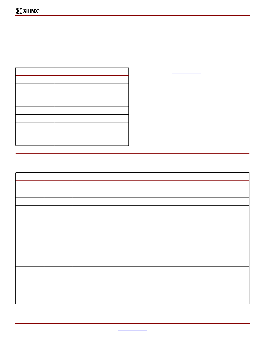
VirtexTM 2.5 V Field Programmable Gate Arrays
R
DS003-2 (v2.8.1) December 9, 2002
www.xilinx.com
Module 2 of 4
Product Specification
1-800-255-7778
19
Data Stream Format
Virtex devices are configured by sequentially loading
frames of data.
Table 11
lists the total number of bits
required to configure each device. For more detailed infor-
mation, see application note XAPP151 "Virtex Configura-
tion Architecture Advanced Users Guide".
Readback
The configuration data stored in the Virtex configuration
memory can be readback for verification. Along with the
configuration data it is possible to readback the contents all
flip-flops/latches, LUTRAMs, and block RAMs. This capabil-
ity is used for real-time debugging.
For more detailed information, see Application Note
XAPP138: Virtex FPGA Series Configuration and Readback,
available online at
www.xilinx.com
.
Revision History
Table 11: Virtex Bit-Stream Lengths
Device
# of Configuration Bits
XCV50
559,200
XCV100
781,216
XCV150
1,040,096
XCV200
1,335,840
XCV300
1,751,808
XCV400
2,546,048
XCV600
3,607,968
XCV800
4,715,616
XCV1000
6,127,744
Date
Version
Revision
11/98
1.0
Initial Xilinx release.
01/99
1.2
Updated package drawings and specs.
02/99
1.3
Update of package drawings, updated specifications.
05/99
1.4
Addition of package drawings and specifications.
05/99
1.5
Replaced FG 676 & FG680 package drawings.
07/99
1.6
Changed Boundary Scan Information and changed Figure 11, Boundary Scan Bit
Sequence. Updated IOB Input & Output delays. Added Capacitance info for different I/O
Standards. Added 5 V tolerant information. Added DLL Parameters and waveforms and
new Pin-to-pin Input and Output Parameter tables for Global Clock Input to Output and
Setup and Hold. Changed Configuration Information including Figures 12, 14, 17 & 19.
Added device-dependent listings for quiescent currents ICCINTQ and ICCOQ. Updated
IOB Input and Output Delays based on default standard of LVTTL, 12 mA, Fast Slew Rate.
Added IOB Input Switching Characteristics Standard Adjustments.
09/99
1.7
Speed grade update to preliminary status, Power-on specification and Clock-to-Out
Minimums additions, "0" hold time listing explanation, quiescent current listing update, and
Figure 6 ADDRA input label correction. Added T
IJITCC
parameter, changed T
OJIT
to T
OPHASE
.
01/00
1.8
Update to speed.txt file 1.96. Corrections for CRs 111036,111137, 112697, 115479,
117153, 117154, and 117612. Modified notes for Recommended Operating Conditions
(voltage and temperature). Changed Bank information for V
CCO
in CS144 package on p.43.

VirtexTM 2.5 V Field Programmable Gate Arrays
R
Module 2 of 4
www.xilinx.com
DS003-2 (v2.8.1) December 9, 2002
20
1-800-255-7778
Product Specification
Virtex Data Sheet
The Virtex Data Sheet contains the following modules:
∑
DS003-1, Virtex 2.5V FPGAs:
Introduction and Ordering Information (Module 1)
∑
DS003-2, Virtex 2.5V FPGAs:
Functional Description (Module 2)
∑
DS003-3, Virtex 2.5V FPGAs:
DC and Switching Characteristics (Module 3)
∑
DS003-4, Virtex 2.5V FPGAs:
Pinout Tables (Module 4)
01/00
1.9
Updated DLL Jitter Parameter table and waveforms, added Delay Measurement
Methodology table for different I/O standards, changed buffered Hex line info and
Input/Output Timing measurement notes.
03/00
2.0
New TBCKO values; corrected FG680 package connection drawing; new note about status
of CCLK pin after configuration.
05/00
2.1
Modified "Pins not listed ..." statement. Speed grade update to Final status.
05/00
2.2
Modified Table 18.
09/00
2.3
∑
Added XCV400 values to table under Minimum Clock-to-Out for Virtex Devices.
∑
Corrected Units column in table under IOB Input Switching Characteristics.
∑
Added values to table under CLB SelectRAM Switching Characteristics.
10/00
2.4
∑
Corrected Pinout information for devices in the BG256, BG432, and BG560 packages in
Table 18.
∑
Corrected BG256 Pin Function Diagram.
04/01
2.5
∑
Revised minimums for Global Clock Set-Up and Hold for LVTTL Standard, with DLL.
∑
Updated SelectMAP Write Timing Characteristics values in
Table 9
.
∑
Converted file to modularized format. See the
Virtex Data Sheet
section.
07/19/01
2.6
∑
Made minor edits to text under
Configuration
.
07/19/02
2.7
∑
Made minor edit to
Figure 16
and
Figure 18
.
09/10/02
2.8
∑
Added clarifications in the
Configuration
,
Boundary-Scan Mode
, and
Block
SelectRAM
sections. Revised
Figure 17
.
12/09/02
2.8.1
∑
Added clarification in the
Boundary Scan
section.
∑
Corrected number of buffered Hex lines listed in
General Purpose Routing
section.
Date
Version
Revision
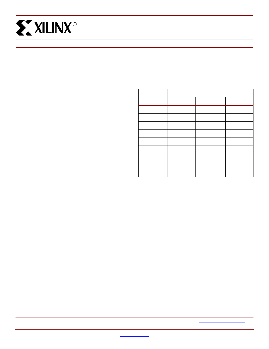
© 1999-2002 Xilinx, Inc. All rights reserved. All Xilinx trademarks, registered trademarks, patents, and disclaimers are as listed at
http://www.xilinx.com/legal.htm
.
All other trademarks and registered trademarks are the property of their respective owners. All specifications are subject to change without notice.
DS003-3 (v3.2) September 10, 2002
www.xilinx.com
Module 3 of 4
Production Product Specification
1-800-255-7778
1
Virtex Electrical Characteristics
Definition of Terms
Electrical and switching characteristics are specified on a
per-speed-grade basis and can be designated as Advance,
Preliminary, or Production. Each designation is defined as
follows:
Advance: These speed files are based on simulations only
and are typically available soon after device design specifi-
cations are frozen. Although speed grades with this desig-
nation are considered relatively stable and conservative,
some under-reporting might still occur.
Preliminary: These speed files are based on complete ES
(engineering sample) silicon characterization. Devices and
speed grades with this designation are intended to give a
better indication of the expected performance of production
silicon. The probability of under-reporting delays is greatly
reduced as compared to Advance data.
Production: These speed files are released once enough
production silicon of a particular device family member has
been characterized to provide full correlation between
speed files and devices over numerous production lots.
There is no under-reporting of delays, and customers
receive formal notification of any subsequent changes. Typ-
ically, the slowest speed grades transition to Production
before faster speed grades.
All specifications are representative of worst-case supply
voltage and junction temperature conditions. The parame-
ters included are common to popular designs and typical
applications. Contact the factory for design considerations
requiring more detailed information.
Table 1
correlates the current status of each Virtex device
with a corresponding speed file designation.
All specifications are subject to change without notice.
0
VirtexTM 2.5 V
Field Programmable Gate Arrays
DS003-3 (v3.2) September 10, 2002
0
0
Production Product Specification
R
Table 1: Virtex Device Speed Grade Designations
Device
Speed Grade Designations
Advance
Preliminary
Production
XCV50
≠6, ≠5, ≠4
XCV100
≠6, ≠5, ≠4
XCV150
≠6, ≠5, ≠4
XCV200
≠6, ≠5, ≠4
XCV300
≠6, ≠5, ≠4
XCV400
≠6, ≠5, ≠4
XCV600
≠6, ≠5, ≠4
XCV800
≠6, ≠5, ≠4
XCV1000
≠6, ≠5, ≠4
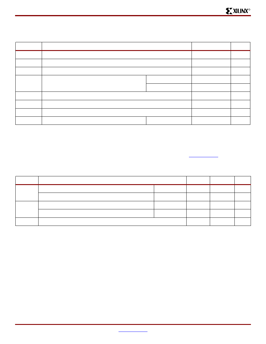
VirtexTM 2.5 V Field Programmable Gate Arrays
R
Module 3 of 4
www.xilinx.com
DS003-3 (v3.2) September 10, 2002
2
1-800-255-7778
Production Product Specification
Virtex DC Characteristics
Absolute Maximum Ratings
Recommended Operating Conditions
Symbol
Description
(1)
Units
V
CCINT
Supply voltage relative to GND
(2)
≠0.5 to 3.0
V
V
CCO
Supply voltage relative to GND
(2)
≠0.5 to 4.0
V
V
REF
Input Reference Voltage
≠0.5 to 3.6
V
V
IN
Input voltage relative to GND
(3)
Using V
REF
≠0.5 to 3.6
V
Internal threshold
≠0.5 to 5.5
V
V
TS
Voltage applied to 3-state output
≠0.5 to 5.5
V
V
CC
Longest Supply Voltage Rise Time from 1V-2.375V
50
ms
T
STG
Storage temperature (ambient)
≠65 to +150
∞C
T
J
Junction temperature
(4)
Plastic Packages
+125
∞C
Notes:
1.
Stresses beyond those listed under Absolute Maximum Ratings can cause permanent damage to the device. These are stress
ratings only, and functional operation of the device at these or any other conditions beyond those listed under Operating Conditions
is not implied. Exposure to Absolute Maximum Ratings conditions for extended periods of time can affect device reliability.
2.
Power supplies can turn on in any order.
3.
For protracted periods (e.g., longer than a day), V
IN
should not exceed V
CCO
by more than 3.6 V.
4.
For soldering guidelines and thermal considerations, see the "Device Packaging" infomation on
www.xilinx.com
.
Symbol
Description
Min
Max
Units
V
CCINT
(1)
Input Supply voltage relative to GND, T
J
= 0
∞C to +85∞C
Commercial
2.5 ≠ 5%
2.5 + 5%
V
Input Supply voltage relative to GND, T
J
= ≠40
∞C to +100∞C Industrial
2.5 ≠ 5%
2.5 + 5%
V
V
CCO
(4)
Supply voltage relative to GND, T
J
= 0
∞C to +85∞C
Commercial
1.4
3.6
V
Supply voltage relative to GND, T
J
= ≠40
∞C to +100∞C
Industrial
1.4
3.6
V
T
IN
Input signal transition time
250
ns
Notes:
1.
Correct operation is guaranteed with a minimum V
CCINT
of 2.375 V (Nominal V
CCINT
≠5%). Below the minimum value, all delay
parameters increase by 3% for each 50-mV reduction in V
CCINT
below the specified range.
2.
At junction temperatures above those listed as Operating Conditions, delay parameters do increase. Please refer to the TRCE report.
3.
Input and output measurement threshold is ~50% of V
CC
.
4.
Min and Max values for V
CCO
are I/O Standard dependant.

VirtexTM 2.5 V Field Programmable Gate Arrays
R
DS003-3 (v3.2) September 10, 2002
www.xilinx.com
Module 3 of 4
Production Product Specification
1-800-255-7778
3
DC Characteristics Over Recommended Operating Conditions
Symbol
Description
Device
Min
Max
Units
V
DRINT
Data Retention V
CCINT
Voltage
(below which configuration data can be lost)
All
2.0
V
V
DRIO
Data Retention V
CCO
Voltage
(below which configuration data can be lost)
All
1.2
V
I
CCINTQ
Quiescent V
CCINT
supply current
(1,3)
XCV50
50
mA
XCV100
50
mA
XCV150
50
mA
XCV200
75
mA
XCV300
75
mA
XCV400
75
mA
XCV600
100
mA
XCV800
100
mA
XCV1000
100
mA
I
CCOQ
Quiescent V
CCO
supply current
(1)
XCV50
2
mA
XCV100
2
mA
XCV150
2
mA
XCV200
2
mA
XCV300
2
mA
XCV400
2
mA
XCV600
2
mA
XCV800
2
mA
XCV1000
2
mA
I
REF
V
REF
current per V
REF
pin
All
20
µA
I
L
Input or output leakage current
All
≠10
+10
µA
C
IN
Input capacitance (sample tested)
BGA, PQ, HQ, packages
All
8
pF
I
RPU
Pad pull-up (when selected) @ V
in
= 0 V, V
CCO
= 3.3 V (sample
tested)
All
Note (2)
0.25
mA
I
RPD
Pad pull-down (when selected) @ V
in
= 3.6 V (sample tested)
Note (2)
0.15
mA
Notes:
1.
With no output current loads, no active input pull-up resistors, all I/O pins 3-stated and floating.
2.
Internal pull-up and pull-down resistors guarantee valid logic levels at unconnected input pins. These pull-up and pull-down resistors
do not guarantee valid logic levels when input pins are connected to other circuits.
3.
Multiply I
CCINTQ
limit by two for industrial grade.
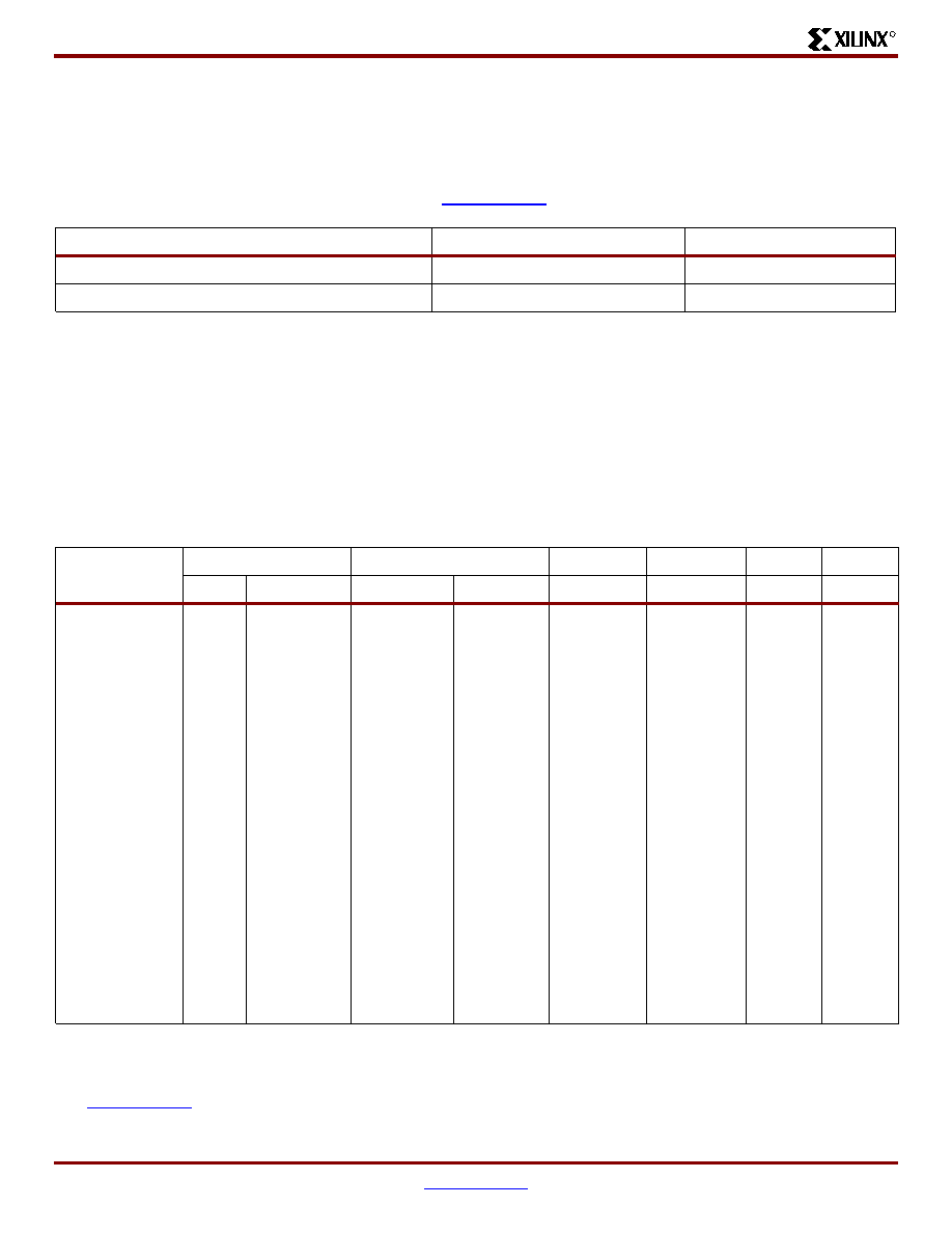
VirtexTM 2.5 V Field Programmable Gate Arrays
R
Module 3 of 4
www.xilinx.com
DS003-3 (v3.2) September 10, 2002
4
1-800-255-7778
Production Product Specification
Power-On Power Supply Requirements
Xilinx FPGAs require a certain amount of supply current during power-on to insure proper device operation. The actual
current consumed depends on the power-on ramp rate of the power supply. This is the time required to reach the nominal
power supply voltage of the device
(1)
from 0 V. The current is highest at the fastest suggested ramp rate (0 V to nominal
voltage in 2 ms) and is lowest at the slowest allowed ramp rate (0 V to nominal voltage in 50 ms). For more details on power
supply requirements, see Application Note XAPP158
on
www.xilinx.com
.
DC Input and Output Levels
Values for V
IL
and V
IH
are recommended input voltages. Values for I
OL
and I
OH
are guaranteed output currents over the
recommended operating conditions at the V
OL
and V
OH
test points. Only selected standards are tested. These are chosen
to ensure that all standards meet their specifications. The selected standards are tested at minimum V
CCO
for each standard
with the respective V
OL
and V
OH
voltage levels shown. Other standards are sample tested.
Product
Description
(2)
Current
Requirement
(1,3)
Virtex Family, Commercial Grade
Minimum required current supply
500 mA
Virtex Family, Industrial Grade
Minimum required current supply
2 A
Notes:
1.
Ramp rate used for this specification is from 0 - 2.7 VDC. Peak current occurs on or near the internal power-on reset threshold of
1.0V and lasts for less than 3 ms.
2.
Devices are guaranteed to initialize properly with the minimum current available from the power supply as noted above.
3.
Larger currents can result if ramp rates are forced to be faster.
Input/Output
Standard
V
IL
V
IH
V
OL
V
OH
I
OL
I
OH
V, min
V, max
V, min
V, max
V, Max
V, Min
mA
mA
LVTTL
(1)
≠ 0.5
0.8
2.0
5.5
0.4
2.4
24
≠24
LVCMOS2
≠ 0.5
.7
1.7
5.5
0.4
1.9
12
≠12
PCI, 3.3 V
≠ 0.5
44% V
CCINT
60% V
CCINT
V
CCO
+ 0.5
10% V
CCO
90% V
CCO
Note 2
Note 2
PCI, 5.0 V
≠ 0.5
0.8
2.0
5.5
0.55
2.4
Note 2
Note 2
GTL
≠ 0.5
V
REF
≠ 0.05
V
REF
+ 0.05
3.6
0.4
n/a
40
n/a
GTL+
≠ 0.5
V
REF
≠ 0.1
V
REF
+ 0.1
3.6
0.6
n/a
36
n/a
HSTL I
(3)
≠ 0.5
V
REF
≠ 0.1
V
REF
+ 0.1
3.6
0.4
V
CCO
≠ 0.4
8
≠8
HSTL III
≠ 0.5
V
REF
≠ 0.1
V
REF
+ 0.1
3.6
0.4
V
CCO
≠ 0.4
24
≠8
HSTL IV
≠ 0.5
V
REF
≠ 0.1
V
REF
+ 0.1
3.6
0.4
V
CCO
≠ 0.4
48
≠8
SSTL3 I
≠ 0.5
V
REF
≠ 0.2
V
REF
+ 0.2
3.6
V
REF
≠ 0.6
V
REF
+ 0.6
8
≠8
SSTL3 II
≠ 0.5
V
REF
≠ 0.2
V
REF
+ 0.2
3.6
V
REF
≠ 0.8
V
REF
+ 0.8
16
≠16
SSTL2 I
≠ 0.5
V
REF
≠ 0.2
V
REF
+ 0.2
3.6
V
REF
≠ 0.61
V
REF
+ 0.61
7.6
≠7.6
SSTL2 II
≠ 0.5
V
REF
≠ 0.2
V
REF
+ 0.2
3.6
V
REF
≠ 0.80
V
REF
+ 0.80
15.2
≠15.2
CTT
≠ 0.5
V
REF
≠ 0.2
V
REF
+ 0.2
3.6
V
REF
≠ 0.4
V
REF
+ 0.4
8
≠8
AGP
≠ 0.5
V
REF
≠ 0.2
V
REF
+ 0.2
3.6
10% V
CCO
90% V
CCO
Note 2
Note 2
Notes:
1.
V
OL
and V
OH
for lower drive currents are sample tested.
2.
Tested according to the relevant specifications.
3.
DC input and output levels for HSTL18 (HSTL I/O standard with V
CCO
of 1.8 V) are provided in an HSTL white paper on
www.xilinx.com
.

VirtexTM 2.5 V Field Programmable Gate Arrays
R
DS003-3 (v3.2) September 10, 2002
www.xilinx.com
Module 3 of 4
Production Product Specification
1-800-255-7778
5
Virtex Switching Characteristics
All devices are 100% functionally tested. Internal timing
parameters are derived from measuring internal test pat-
terns. Listed below are representative values. For more
specific, more precise, and worst-case guaranteed data,
use the values reported by the static timing analyzer (TRCE
in the Xilinx Development System) and back-annotated to
the simulation net list. All timing parameters assume
worst-case operating conditions (supply voltage and junc-
tion temperature). Values apply to all Virtex devices unless
otherwise noted.
IOB Input Switching Characteristics
Input delays associated with the pad are specified for LVTTL levels. For other standards, adjust the delays with the values
shown in
, page 6
.
Description
Device
Symbol
Speed Grade
Units
Min
-6
-5
-4
Propagation Delays
Pad to I output, no delay
All
T
IOPI
0.39
0.8
0.9
1.0
ns, max
Pad to I output, with delay
XCV50
T
IOPID
0.8
1.5
1.7
1.9
ns, max
XCV100
0.8
1.5
1.7
1.9
ns, max
XCV150
0.8
1.5
1.7
1.9
ns, max
XCV200
0.8
1.5
1.7
1.9
ns, max
XCV300
0.8
1.5
1.7
1.9
ns, max
XCV400
0.9
1.8
2.0
2.3
ns, max
XCV600
0.9
1.8
2.0
2.3
ns, max
XCV800
1.1
2.1
2.4
2.7
ns, max
XCV1000
1.1
2.1
2.4
2.7
ns, max
Pad to output IQ via transparent
latch, no delay
All
T
IOPLI
0.8
1.6
1.8
2.0
ns, max
Pad to output IQ via transparent
latch, with delay
XCV50
T
IOPLID
1.9
3.7
4.2
4.8
ns, max
XCV100
1.9
3.7
4.2
4.8
ns, max
XCV150
2.0
3.9
4.3
4.9
ns, max
XCV200
2.0
4.0
4.4
5.1
ns, max
XCV300
2.0
4.0
4.4
5.1
ns, max
XCV400
2.1
4.1
4.6
5.3
ns, max
XCV600
2.1
4.2
4.7
5.4
ns, max
XCV800
2.2 4.4
4.9
5.6
ns,
max
XCV1000
2.3
4.5
5.1
5.8
ns, max
Sequential Delays
Clock CLK
All
Minimum Pulse Width, High
T
CH
0.8
1.5
1.7
2.0
ns, min
Minimum Pulse Width, Low
T
CL
0.8
1.5
1.7
2.0
ns, min
Clock CLK to output IQ
T
IOCKIQ
0.2
0.7
0.7
0.8
ns, max
VirtexTM 2.5 V Field Programmable Gate Arrays
R
Module 3 of 4
www.xilinx.com
DS003-3 (v3.2) September 10, 2002
6
1-800-255-7778
Production Product Specification
Setup and Hold Times with respect to Clock CLK at IOB input
register
(1)
Setup Time / Hold Time
Pad, no delay
All
T
IOPICK
/T
IOICKP
0.8 / 0
1.6 / 0
1.8 / 0
2.0 / 0
ns, min
Pad, with delay
XCV50
T
IOPICKD
/T
IOICKPD
1.9 / 0
3.7 / 0
4.1 / 0
4.7 / 0
ns, min
XCV100
1.9 / 0
3.7 / 0
4.1 / 0
4.7 / 0
ns, min
XCV150
1.9 / 0
3.8 / 0
4.3 / 0
4.9 / 0
ns, min
XCV200
2.0 / 0
3.9 / 0
4.4 / 0
5.0 / 0
ns, min
XCV300
2.0 / 0
3.9 / 0
4.4 / 0
5.0 / 0
ns, min
XCV400
2.1 / 0
4.1 / 0
4.6 / 0
5.3 / 0
ns, min
XCV600
2.1 / 0
4.2 / 0
4.7 / 0
5.4 / 0
ns, min
XCV800
2.2 / 0
4.4 / 0
4.9 / 0
5.6 / 0
ns, min
XCV1000
2.3 / 0
4.5 / 0
5.0 / 0
5.8 / 0
ns, min
ICE input
All
T
IOICECK
/T
IOCKICE
0.37/ 0
0.8 / 0
0.9 / 0
1.0 / 0
ns, max
Set/Reset Delays
SR input (IFF, synchronous)
All
T
IOSRCKI
0.49
1.0
1.1
1.3
ns, max
SR input to IQ (asynchronous)
All
T
IOSRIQ
0.70
1.4
1.6
1.8
ns, max
GSR to output IQ
All
T
GSRQ
4.9
9.7
10.9
12.5
ns, max
Notes:
1.
A Zero "0" Hold Time listing indicates no hold time or a negative hold time. Negative values cannot be guaranteed "best-case", but
if a "0" is listed, there is no positive hold time.
2.
Input timing for LVTTL is measured at 1.4 V. For other I/O standards, see
Table 3
.
Description
Device
Symbol
Speed Grade
Units
Min
-6
-5
-4
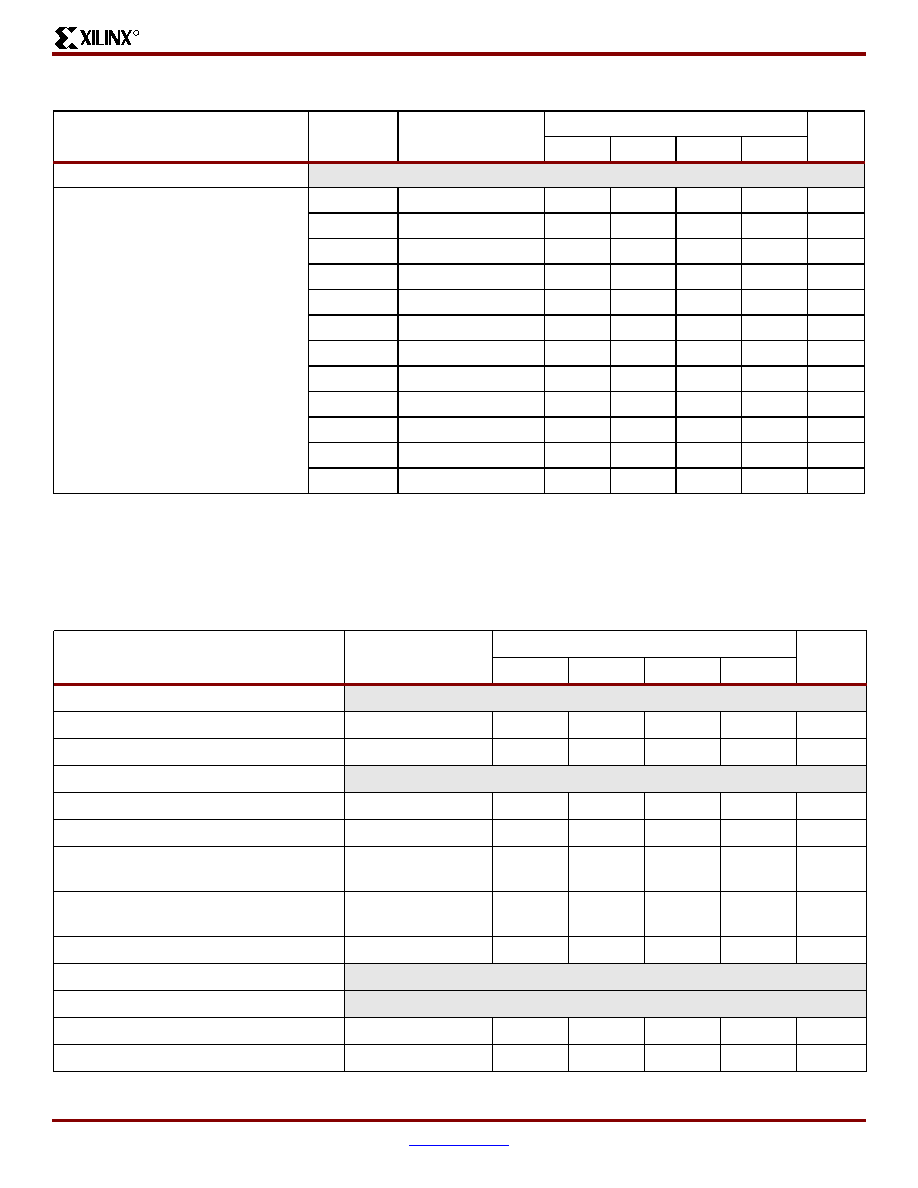
VirtexTM 2.5 V Field Programmable Gate Arrays
R
DS003-3 (v3.2) September 10, 2002
www.xilinx.com
Module 3 of 4
Production Product Specification
1-800-255-7778
7
IOB Input Switching Characteristics Standard Adjustments
IOB Output Switching Characteristics
Output delays terminating at a pad are specified for LVTTL with 12 mA drive and fast slew rate. For other standards, adjust
the delays with the values shown in IOB Output Switching Characteristics Standard Adjustments
, page 9
.
Description
Symbol
Standard
(1)
Speed Grade
Units
Min
-6
-5
-4
Data Input Delay Adjustments
Standard-specific data input delay
adjustments
T
ILVTTL
LVTTL
0
0
0
0
ns
T
ILVCMOS2
LVCMOS2
≠0.02
≠0.04
≠0.04
≠0.05
ns
T
IPCI33_3
PCI, 33 MHz, 3.3 V
≠0.05
≠0.11
≠0.12
≠0.14
ns
T
IPCI33_5
PCI, 33 MHz, 5.0 V
0.13
0.25
0.28
0.33
ns
T
IPCI66_3
PCI, 66 MHz, 3.3 V
≠0.05
≠0.11
≠0.12
≠0.14
ns
T
IGTL
GTL
0.10
0.20
0.23
0.26
ns
T
IGTLP
GTL+
0.06
0.11
0.12
0.14
ns
T
IHSTL
HSTL
0.02
0.03
0.03
0.04
ns
T
ISSTL2
SSTL2
≠0.04
≠0.08
≠0.09
≠0.10
ns
T
ISSTL3
SSTL3
≠0.02
≠0.04
≠0.05
≠0.06
ns
T
ICTT
CTT
0.01
0.02
0.02
0.02
ns
T
IAGP
AGP
≠0.03
≠0.06
≠0.07
≠0.08
ns
Notes:
1.
Input timing for LVTTL is measured at 1.4 V. For other I/O standards, see
Table 3
.
Description
Symbol
Speed Grade
Units
Min
-6
-5
-4
Propagation Delays
O input to Pad
T
IOOP
1.2
2.9
3.2
3.5
ns, max
O input to Pad via transparent latch
T
IOOLP
1.4
3.4
3.7
4.0
ns, max
3-State Delays
T input to Pad high-impedance
(1)
T
IOTHZ
1.0
2.0
2.2
2.4
ns, max
T input to valid data on Pad
T
IOTON
1.4
3.1
3.3
3.7
ns, max
T input to Pad high-impedance via
transparent latch
(1)
T
IOTLPHZ
1.2
2.4
2.6
3.0
ns, max
T input to valid data on Pad via
transparent latch
T
IOTLPON
1.6
3.5
3.8
4.2
ns, max
GTS to Pad high impedance
(1)
T
GTS
2.5
4.9
5.5
6.3
ns, max
Sequential Delays
Clock CLK
Minimum Pulse Width, High
T
CH
0.8
1.5
1.7
2.0
ns, min
Minimum Pulse Width, Low
T
CL
0.8
1.5
1.7
2.0
ns, min
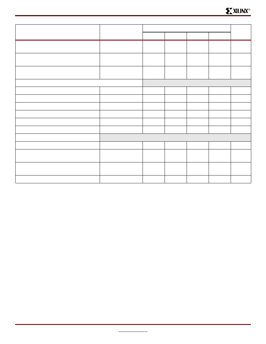
VirtexTM 2.5 V Field Programmable Gate Arrays
R
Module 3 of 4
www.xilinx.com
DS003-3 (v3.2) September 10, 2002
8
1-800-255-7778
Production Product Specification
Clock CLK to Pad delay with OBUFT
enabled (non-3-state)
T
IOCKP
1.0
2.9
3.2
3.5
ns, max
Clock CLK to Pad high-impedance
(synchronous)
(1)
T
IOCKHZ
1.1
2.3
2.5
2.9
ns, max
Clock CLK to valid data on Pad delay, plus
enable delay for OBUFT
T
IOCKON
1.5
3.4
3.7
4.1
ns, max
Setup and Hold Times before/after Clock CLK
(2)
Setup Time / Hold Time
O input
T
IOOCK
/T
IOCKO
0.51 / 0
1.1 / 0
1.2 / 0
1.3 / 0
ns, min
OCE input
T
IOOCECK
/T
IOCKOCE
0.37 / 0
0.8 / 0
0.9 / 0
1.0 / 0
ns, min
SR input (OFF)
T
IOSRCKO
/T
IOCKOSR
0.52 / 0
1.1 / 0
1.2 / 0
1.4 / 0
ns, min
3-State Setup Times, T input
T
IOTCK
/T
IOCKT
0.34 / 0
0.7 / 0
0.8 / 0
0.9 / 0
ns, min
3-State Setup Times, TCE input
T
IOTCECK
/T
IOCKTCE
0.41 / 0
0.9 / 0
0.9 / 0
1.1 / 0
ns, min
3-State Setup Times, SR input (TFF)
T
IOSRCKT
/T
IOCKTSR
0.49 / 0
1.0 / 0
1.1 / 0
1.3 / 0
ns, min
Set/Reset Delays
SR input to Pad (asynchronous)
T
IOSRP
1.6
3.8
4.1
4.6
ns, max
SR input to Pad high-impedance
(asynchronous)
(1)
T
IOSRHZ
1.6
3.1
3.4
3.9
ns, max
SR input to valid data on Pad
(asynchronous)
T
IOSRON
2.0
4.2
4.6
5.1
ns, max
GSR to Pad
T
IOGSRQ
4.9
9.7
10.9
12.5
ns, max
Notes:
1.
3-state turn-off delays should not be adjusted.
2.
A Zero "0" Hold Time listing indicates no hold time or a negative hold time. Negative values can not be guaranteed "best-case", but
if a "0" is listed, there is no positive hold time.
Description
Symbol
Speed Grade
Units
Min
-6
-5
-4
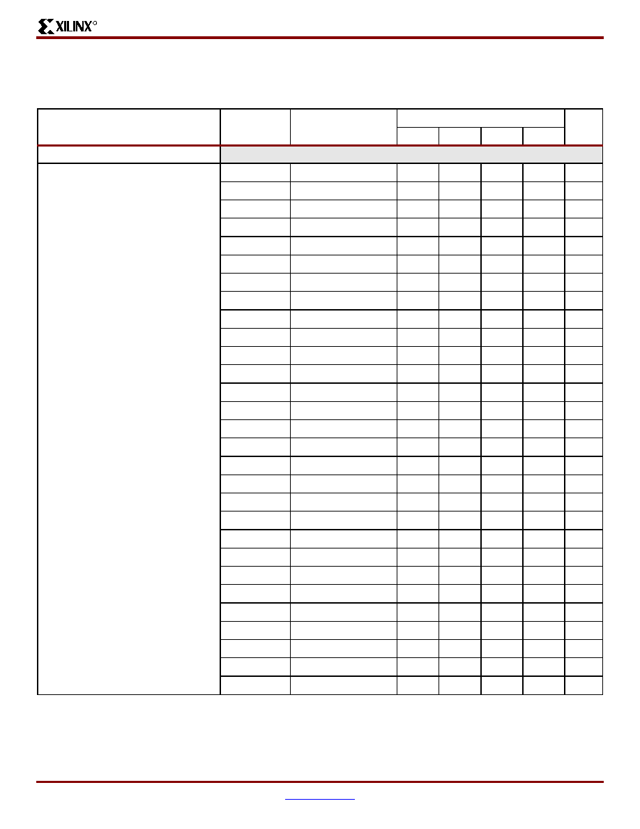
VirtexTM 2.5 V Field Programmable Gate Arrays
R
DS003-3 (v3.2) September 10, 2002
www.xilinx.com
Module 3 of 4
Production Product Specification
1-800-255-7778
9
IOB Output Switching Characteristics Standard Adjustments
Output delays terminating at a pad are specified for LVTTL with 12 mA drive and fast slew rate. For other standards, adjust
the delays by the values shown.
Description
Symbol
Standard
(1)
Speed Grade
Unit
s
Min
-6
-5
-4
Output Delay Adjustments
Standard-specific adjustments for
output delays terminating at pads
(based on standard capacitive load,
Csl)
T
OLVTTL_S2
LVTTL, Slow, 2 mA
4.2
14.7
15.8
17.0
ns
T
OLVTTL_S4
4 mA
2.5
7.5
8.0
8.6
ns
T
OLVTTL_S6
6 mA
1.8
4.8
5.1
5.6
ns
T
OLVTTL_S8
8 mA
1.2
3.0
3.3
3.5
ns
T
OLVTTL_S12
12 mA
1.0
1.9
2.1
2.2
ns
T
OLVTTL_S16
16 mA
0.9
1.7
1.9
2.0
ns
T
OLVTTL_S24
24 mA
0.8
1.3
1.4
1.6
ns
T
OLVTTL_F2
LVTTL, Fast, 2mA
1.9
13.1
14.0
15.1
ns
T
OLVTTL_F4
4 mA
0.7
5.3
5.7
6.1
ns
T
OLVTTL_F6
6 mA
0.2
3.1
3.3
3.6
ns
T
OLVTTL_F8
8 mA
0.1
1.0
1.1
1.2
ns
T
OLVTTL_F12
12 mA
0
0
0
0
ns
T
OLVTTL_F16
16 mA
≠0.10
≠0.05
≠0.05
≠0.05
ns
T
OLVTTL_F24
24 mA
≠0.10
≠0.20
≠0.21
≠0.23
ns
T
OLVCMOS2
LVCMOS2
0.10
0.10
0.11
0.12
ns
T
OPCI33_3
PCI, 33 MHz, 3.3 V
0.50
2.3
2.5
2.7
ns
T
OPCI33_5
PCI, 33 MHz, 5.0 V
0.40
2.8
3.0
3.3
ns
T
OPCI66_3
PCI, 66 MHz, 3.3 V
0.10
≠0.40
≠0.42
≠0.46
ns
T
OGTL
GTL
0.6
0.50
0.54
0.6
ns
T
OGTLP
GTL+
0.7
0.8
0.9
1.0
ns
T
OHSTL_I
HSTL I
0.10
≠0.50
≠0.53
≠0.5
ns
T
OHSTL_III
HSTL III
≠0.10
≠0.9
≠0.9
≠1.0
ns
T
OHSTL_IV
HSTL IV
≠0.20
≠1.0
≠1.0
≠1.1
ns
T
OSSTL2_I
SSTL2 I
≠0.10
≠0.50
≠0.53
≠0.5
ns
T
OSSLT2_II
SSTL2 II
≠0.20
≠0.9
≠0.9
≠1.0
ns
T
OSSTL3_I
SSTL3 I
≠0.20
≠0.50
≠0.53
≠0.5
ns
T
OSSTL3_II
SSTL3 II
≠0.30
≠1.0
≠1.0
≠1.1
ns
T
OCTT
CTT
0
≠0.6
≠0.6
≠0.6
ns
T
OAGP
AGP
0
≠0.9
≠0.9
≠1.0
ns
Notes:
1.
Output timing is measured at 1.4 V with 35 pF external capacitive load for LVTTL. For other I/O standards and different loads, see
Table 2
and
Table 3
.
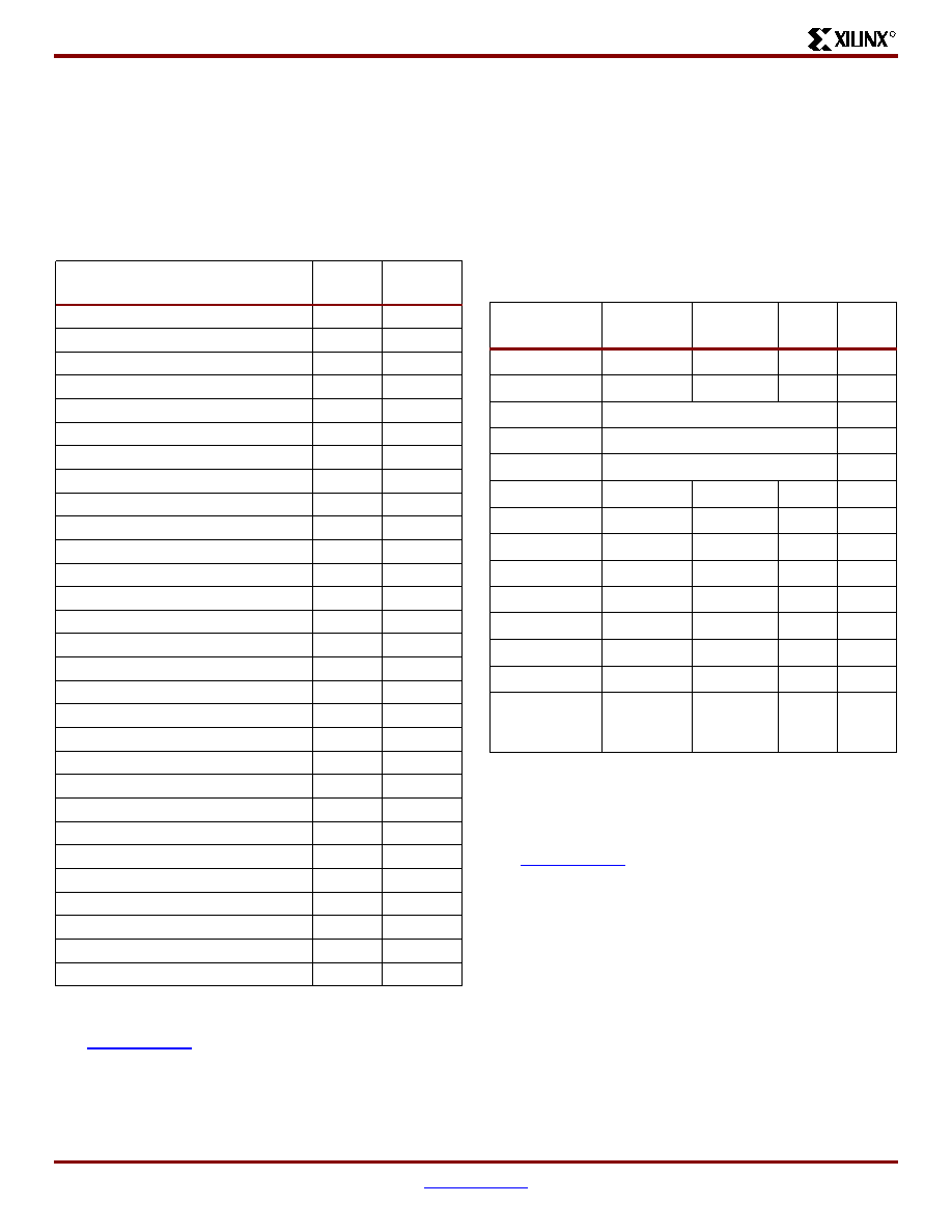
VirtexTM 2.5 V Field Programmable Gate Arrays
R
Module 3 of 4
www.xilinx.com
DS003-3 (v3.2) September 10, 2002
10
1-800-255-7778
Production Product Specification
Calculation of T
ioop
as a Function of
Capacitance
T
ioop
is the propagation delay from the O Input of the IOB to
the pad. The values for T
ioop
were based on the standard
capacitive load (Csl) for each I/O standard as listed in
Table 2
.
For other capacitive loads, use the formulas below to calcu-
late the corresponding T
ioop
.
T
ioop
= T
ioop
+ T
opadjust
+
(C
load
≠ C
sl
) * fl
Where:
T
opadjust
is reported above in the Output Delay
Adjustment section.
C
load
is the capacitive load for the design.
Table 2: Constants for Calculating T
ioop
Standard
Csl
(pF)
fl
(ns/pF)
LVTTL Fast Slew Rate, 2mA drive
35
0.41
LVTTL Fast Slew Rate, 4mA drive
35
0.20
LVTTL Fast Slew Rate, 6mA drive
35
0.13
LVTTL Fast Slew Rate, 8mA drive
35
0.079
LVTTL Fast Slew Rate, 12mA drive
35
0.044
LVTTL Fast Slew Rate, 16mA drive
35
0.043
LVTTL Fast Slew Rate, 24mA drive
35
0.033
LVTTL Slow Slew Rate, 2mA drive
35
0.41
LVTTL Slow Slew Rate, 4mA drive
35
0.20
LVTTL Slow Slew Rate, 6mA drive
35
0.100
LVTTL Slow Slew Rate, 8mA drive
35
0.086
LVTTL Slow Slew Rate, 12mA drive
35
0.058
LVTTL Slow Slew Rate, 16mA drive
35
0.050
LVTTL Slow Slew Rate, 24mA drive
35
0.048
LVCMOS2
35
0.041
PCI 33MHz 5V
50
0.050
PCI 33MHZ 3.3 V
10
0.050
PCI 66 MHz 3.3 V
10
0.033
GTL
0
0.014
GTL+
0
0.017
HSTL Class I
20
0.022
HSTL Class III
20
0.016
HSTL Class IV
20
0.014
SSTL2 Class I
30
0.028
SSTL2 Class II
30
0.016
SSTL3 Class I
30
0.029
SSTL3 Class II
30
0.016
CTT
20
0.035
AGP
10
0.037
Notes:
1.
I/O parameter measurements are made with the capacitance
values shown above. See Application Note XAPP133 on
www.xilinx.com
for appropriate terminations.
2.
I/O standard measurements are reflected in the IBIS model
information except where the IBIS format precludes it.
Table 3: Delay Measurement Methodology
Standard
V
L
(1)
V
H
(1)
Meas.
Point
V
REF
Typ
(2)
LVTTL
0
3
1.4
-
LVCMOS2
0
2.5
1.125
-
PCI33_5
Per PCI Spec
-
PCI33_3
Per PCI Spec
-
PCI66_3
Per PCI Spec
-
GTL
V
REF
≠0.2
V
REF
+0.2
V
REF
0.80
GTL+
V
REF
≠0.2
V
REF
+0.2
V
REF
1.0
HSTL Class I
V
REF
≠0.5
V
REF
+0.5
V
REF
0.75
HSTL Class III
V
REF
≠0.5
V
REF
+0.5
V
REF
0.90
HSTL Class IV
V
REF
≠0.5
V
REF
+0.5
V
REF
0.90
SSTL3 I & II
V
REF
≠1.0
V
REF
+1.0
V
REF
1.5
SSTL2 I & II
V
REF
≠0.75
V
REF
+0.75
V
REF
1.25
CTT
V
REF
≠0.2
V
REF
+0.2
V
REF
1.5
AGP
V
REF
≠
(0.2xV
CCO
)
V
REF
+
(0.2xV
CCO
)
V
REF
Per
AGP
Spec
Notes:
1.
Input waveform switches between V
L
and V
H
.
2.
Measurements are made at VREF (Typ), Maximum, and
Minimum. Worst-case values are reported.
3.
I/O parameter measurements are made with the capacitance
values shown in
Table 2
. See Application Note XAPP133
on
www.xilinx.com
for appropriate terminations.
4.
I/O standard measurements are reflected in the IBIS model
information except where the IBIS format precludes it.
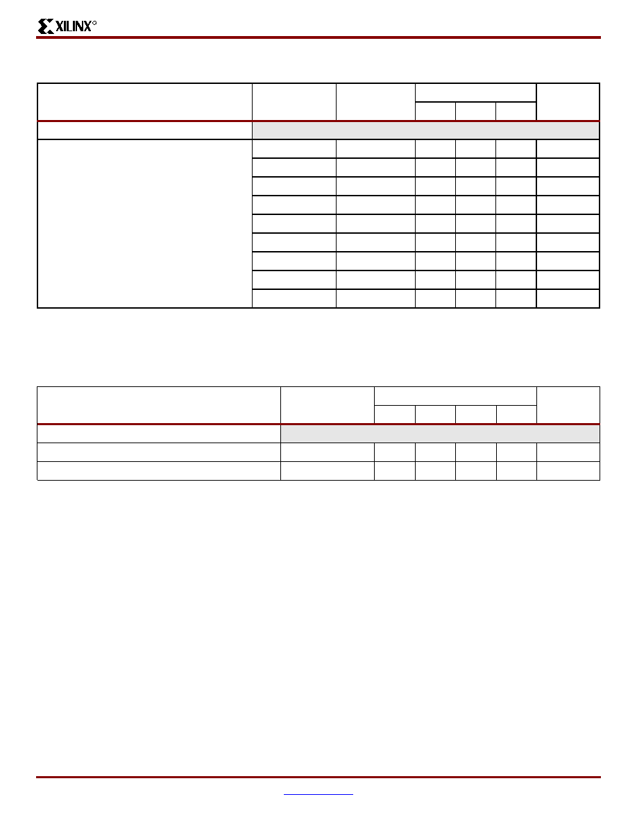
VirtexTM 2.5 V Field Programmable Gate Arrays
R
DS003-3 (v3.2) September 10, 2002
www.xilinx.com
Module 3 of 4
Production Product Specification
1-800-255-7778
11
Clock Distribution Guidelines
Clock Distribution Switching Characteristics
Description
Device
Symbol
Speed Grade
Units
-6
-5
-4
Global Clock Skew
(1)
Global Clock Skew between IOB Flip-flops
XCV50
T
GSKEWIOB
0.10
0.12
0.14
ns, max
XCV100
0.12
0.13
0.15
ns, max
XCV150
0.12
0.13
0.15
ns, max
XCV200
0.13
0.14
0.16
ns, max
XCV300
0.14
0.16
0.18
ns, max
XCV400
0.13
0.13
0.14
ns, max
XCV600
0.14
0.15
0.17
ns, max
XCV800
0.16
0.17
0.20
ns, max
XCV1000
0.20
0.23
0.25
ns, max
Notes:
1.
These clock-skew delays are provided for guidance only. They reflect the delays encountered in a typical design under worst-case
conditions. Precise values for a particular design are provided by the timing analyzer.
Description
Symbol
Speed Grade
Units
Min
-6
-5
-4
GCLK IOB and Buffer
Global Clock PAD to output.
T
GPIO
0.33
0.7
0.8
0.9
ns, max
Global Clock Buffer I input to O output
T
GIO
0.34
0.7
0.8
0.9
ns, max
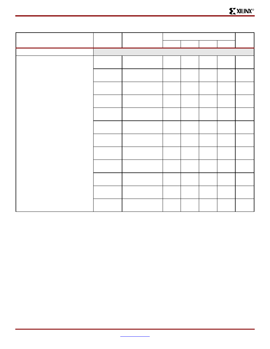
VirtexTM 2.5 V Field Programmable Gate Arrays
R
Module 3 of 4
www.xilinx.com
DS003-3 (v3.2) September 10, 2002
12
1-800-255-7778
Production Product Specification
I/O Standard Global Clock Input Adjustments
Description
Symbol
Standard
(1)
Speed Grade
Units
Min
-6
-5
-4
Data Input Delay Adjustments
Standard-specific global clock input
delay adjustments
T
GPLVTTL
LVTTL
0
0
0
0
ns,
max
T
GPLVCMOS
2
LVCMOS2
≠0.02
≠0.04
≠0.04
≠0.05
ns,
max
T
GPPCI33_3
PCI, 33 MHz, 3.3
V
≠0.05
≠0.11
≠0.12
≠0.14
ns,
max
T
GPPCI33_5
PCI, 33 MHz, 5.0
V
0.13
0.25
0.28
0.33
ns,
max
T
GPPCI66_3
PCI, 66 MHz, 3.3
V
≠0.05
≠0.11
≠0.12
≠0.14
ns,
max
T
GPGTL
GTL
0.7
0.8
0.9
0.9
ns,
max
T
GPGTLP
GTL+
0.7
0.8
0.8
0.8
ns,
max
T
GPHSTL
HSTL
0.7
0.7
0.7
0.7
ns,
max
T
GPSSTL2
SSTL2
0.6
0.52
0.51
0.50
ns,
max
T
GPSSTL3
SSTL3
0.6
0.6
0.55
0.54
ns,
max
T
GPCTT
CTT
0.7
0.7
0.7
0.7
ns,
max
T
GPAGP
AGP
0.6
0.54
0.53
0.52
ns,
max
Notes:
1.
Input timing for GPLVTTL is measured at 1.4 V. For other I/O standards, see
Table 3
.
VirtexTM 2.5 V Field Programmable Gate Arrays
R
DS003-3 (v3.2) September 10, 2002
www.xilinx.com
Module 3 of 4
Production Product Specification
1-800-255-7778
13
CLB Switching Characteristics
Delays originating at F/G inputs vary slightly according to the input used. The values listed below are worst-case. Precise
values are provided by the timing analyzer.
Description
Symbol
Speed Grade
Units
Min
-6
-5
-4
Combinatorial Delays
4-input function: F/G inputs to X/Y outputs
T
ILO
0.29
0.6
0.7
0.8
ns, max
5-input function: F/G inputs to F5 output
T
IF5
0.32
0.7
0.8
0.9
ns, max
5-input function: F/G inputs to X output
T
IF5X
0.36
0.8
0.8
1.0
ns, max
6-input function: F/G inputs to Y output via F6 MUX
T
IF6Y
0.44
0.9
1.0
1.2
ns, max
6-input function: F5IN input to Y output
T
F5INY
0.17
0.32
0.36
0.42
ns, max
Incremental delay routing through transparent latch
to XQ/YQ outputs
T
IFNCTL
0.31
0.7
0.7
0.8
ns, max
BY input to YB output
T
BYYB
0.27
0.53
0.6
0.7
ns, max
Sequential Delays
FF Clock CLK to XQ/YQ outputs
T
CKO
0.54
1.1
1.2
1.4
ns, max
Latch Clock CLK to XQ/YQ outputs
T
CKLO
0.6
1.2
1.4
1.6
ns, max
Setup and Hold Times before/after Clock CLK
(1)
Setup Time / Hold Time
4-input function: F/G Inputs
T
ICK
/T
CKI
0.6 / 0
1.2 / 0
1.4 / 0
1.5 / 0
ns, min
5-input function: F/G inputs
T
IF5CK
/T
CKIF5
0.7 / 0
1.3 / 0
1.5 / 0
1.7 / 0
ns, min
6-input function: F5IN input
T
F5INCK
/T
CKF5IN
0.46 / 0
1.0 / 0
1.1 / 0
1.2 / 0
ns, min
6-input function: F/G inputs via F6 MUX
T
IF6CK
/T
CKIF6
0.8 / 0
1.5 / 0
1.7 / 0
1.9 / 0
ns, min
BX/BY inputs
T
DICK
/T
CKDI
0.30 / 0
0.6 / 0
0.7 / 0
0.8 / 0
ns, min
CE input
T
CECK
/T
CKCE
0.37 / 0
0.8 / 0
0.9 / 0
1.0 / 0
ns, min
SR/BY inputs (synchronous)
T
RCK
T
CKR
0.33 / 0
0.7 / 0
0.8 / 0
0.9 / 0
ns, min
Clock CLK
Minimum Pulse Width, High
T
CH
0.8
1.5
1.7
2.0
ns, min
Minimum Pulse Width, Low
T
CL
0.8
1.5
1.7
2.0
ns, min
Set/Reset
Minimum Pulse Width, SR/BY inputs
T
RPW
1.3
2.5
2.8
3.3
ns, min
Delay from SR/BY inputs to XQ/YQ outputs
(asynchronous)
T
RQ
0.54
1.1
1.3
1.4
ns, max
Delay from GSR to XQ/YQ outputs
T
IOGSRQ
4.9
9.7
10.9
12.5
ns, max
Toggle Frequency (MHz) (for export control)
F
TOG
(MHz)
625
333
294
250
MHz
Notes:
1.
A Zero "0" Hold Time listing indicates no hold time or a negative hold time. Negative values cannot be guaranteed "best-case", but
if a "0" is listed, there is no positive hold time.
VirtexTM 2.5 V Field Programmable Gate Arrays
R
Module 3 of 4
www.xilinx.com
DS003-3 (v3.2) September 10, 2002
14
1-800-255-7778
Production Product Specification
CLB Arithmetic Switching Characteristics
Setup times not listed explicitly can be approximated by decreasing the combinatorial delays by the setup time adjustment
listed. Precise values are provided by the timing analyzer.
Description
Symbol
Speed Grade
Units
Min
-6
-5
-4
Combinatorial Delays
F operand inputs to X via XOR
T
OPX
0.37
0.8
0.9
1.0
ns, max
F operand input to XB output
T
OPXB
0.54
1.1
1.3
1.4
ns, max
F operand input to Y via XOR
T
OPY
0.8
1.5
1.7
2.0
ns, max
F operand input to YB output
T
OPYB
0.8
1.5
1.7
2.0
ns, max
F operand input to COUT output
T
OPCYF
0.6
1.2
1.3
1.5
ns, max
G operand inputs to Y via XOR
T
OPGY
0.46
1.0
1.1
1.2
ns, max
G operand input to YB output
T
OPGYB
0.8
1.6
1.8
2.1
ns, max
G operand input to COUT output
T
OPCYG
0.7
1.3
1.4
1.6
ns, max
BX initialization input to COUT
T
BXCY
0.41
0.9
1.0
1.1
ns, max
CIN input to X output via XOR
T
CINX
0.21
0.41
0.46
0.53
ns, max
CIN input to XB
T
CINXB
0.02
0.04
0.05
0.06
ns, max
CIN input to Y via XOR
T
CINY
0.23
0.46
0.52
0.6
ns, max
CIN input to YB
T
CINYB
0.23
0.45
0.51
0.6
ns, max
CIN input to COUT output
T
BYP
0.05
0.09
0.10
0.11
ns, max
Multiplier Operation
F1/2 operand inputs to XB output via AND
T
FANDXB
0.18
0.36
0.40
0.46
ns, max
F1/2 operand inputs to YB output via AND
T
FANDYB
0.40
0.8
0.9
1.1
ns, max
F1/2 operand inputs to COUT output via AND
T
FANDCY
0.22
0.43
0.48
0.6
ns, max
G1/2 operand inputs to YB output via AND
T
GANDYB
0.25
0.50
0.6
0.7
ns, max
G1/2 operand inputs to COUT output via AND
T
GANDCY
0.07
0.13
0.15
0.17
ns, max
Setup and Hold Times before/after Clock CLK
(1)
Setup Time / Hold Time
CIN input to FFX
T
CCKX
/T
CKCX
0.50 / 0
1.0 / 0
1.2 / 0
1.3 / 0
ns, min
CIN input to FFY
T
CCKY
/T
CKCY
0.53 / 0
1.1 / 0
1.2 / 0
1.4 / 0
ns, min
Notes:
1.
A Zero "0" Hold Time listing indicates no hold time or a negative hold time. Negative values can not be guaranteed "best-case", but
if a "0" is listed, there is no positive hold time.

VirtexTM 2.5 V Field Programmable Gate Arrays
R
DS003-3 (v3.2) September 10, 2002
www.xilinx.com
Module 3 of 4
Production Product Specification
1-800-255-7778
15
CLB SelectRAM Switching Characteristics
Description
Symbol
Speed Grade
Units
Min
-6
-5
-4
Sequential Delays
Clock CLK to X/Y outputs (WE active) 16 x 1 mode
T
SHCKO16
1.2
2.3
2.6
3.0
ns, max
Clock CLK to X/Y outputs (WE active) 32 x 1 mode
T
SHCKO32
1.2
2.7
3.1
3.5
ns, max
Shift-Register Mode
Clock CLK to X/Y outputs
T
REG
1.2
3.7
4.1
4.7
ns, max
Setup and Hold Times before/after Clock CLK
(1)
Setup Time / Hold Time
F/G address inputs
T
AS
/T
AH
0.25 / 0
0.5 / 0
0.6 / 0
0.7 / 0
ns, min
BX/BY data inputs (DIN)
T
DS
/T
DH
0.34 / 0
0.7 / 0
0.8 / 0
0.9 / 0
ns, min
CE input (WE)
T
WS
/T
WH
0.38 / 0
0.8 / 0
0.9 / 0
1.0 / 0
ns, min
Shift-Register Mode
BX/BY data inputs (DIN)
T
SHDICK
0.34
0.7 0.8
0.9
ns,
min
CE input (WS)
T
SHCECK
0.38
0.8
0.9
1.0
ns, min
Clock CLK
Minimum Pulse Width, High
T
WPH
1.2
2.4
2.7
3.1
ns, min
Minimum Pulse Width, Low
T
WPL
1.2
2.4
2.7
3.1
ns, min
Minimum clock period to meet address write cycle
time
T
WC
2.4
4.8
5.4
6.2
ns, min
Shift-Register Mode
Minimum Pulse Width, High
T
SRPH
1.2
2.4
2.7
3.1
ns, min
Minimum Pulse Width, Low
T
SRPL
1.2
2.4
2.7
3.1
ns, min
Notes:
1.
A Zero "0" Hold Time listing indicates no hold time or a negative hold time. Negative values can not be guaranteed "best-case", but
if a "0" is listed, there is no positive hold time.
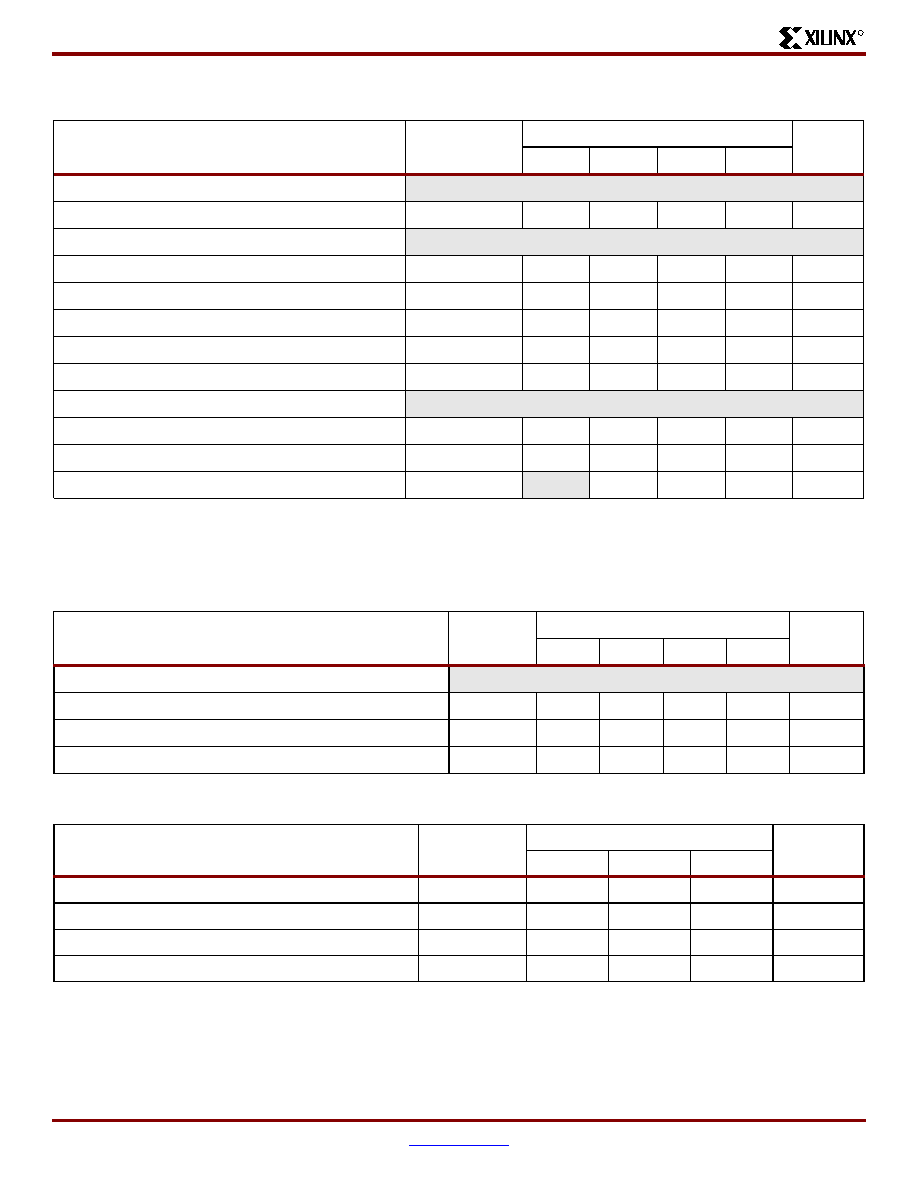
VirtexTM 2.5 V Field Programmable Gate Arrays
R
Module 3 of 4
www.xilinx.com
DS003-3 (v3.2) September 10, 2002
16
1-800-255-7778
Production Product Specification
Block RAM Switching Characteristics
TBUF Switching Characteristics
JTAG Test Access Port Switching Characteristics
Description
Symbol
Speed Grade
Units
Min
-6
-5
-4
Sequential Delays
Clock CLK to DOUT output
T
BCKO
1.7
3.4
3.8
4.3
ns, max
Setup and Hold Times before/after Clock CLK
(1)
Setup Time / Hold Time
ADDR inputs
T
BACK
/T
BCKA
0.6 / 0
1.2 / 0
1.3 / 0
1.5 / 0
ns, min
DIN inputs
T
BDCK
/T
BCKD
0.6 / 0
1.2 / 0
1.3 / 0
1.5 / 0
ns, min
EN input
T
BECK
/T
BCKE
1.3 / 0
2.6 / 0
3.0 / 0
3.4 / 0
ns, min
RST input
T
BRCK
/T
BCKR
1.3 / 0
2.5 / 0
2.7 / 0
3.2 / 0
ns, min
WEN input
T
BWCK
/T
BCKW
1.2 / 0
2.3 / 0
2.6 / 0
3.0 / 0
ns, min
Clock CLK
Minimum Pulse Width, High
T
BPWH
0.8
1.5
1.7
2.0
ns, min
Minimum Pulse Width, Low
T
BPWL
0.8
1.5
1.7
2.0
ns, min
CLKA -> CLKB setup time for different ports
T
BCCS
3.0
3.5
4.0
ns, min
Notes:
1.
A Zero "0" Hold Time listing indicates no hold time or a negative hold time. Negative values can not be guaranteed "best-case", but
if a "0" is listed, there is no positive hold time.
Description
Symbol
Speed Grade
Units
Min
-6
-5
-4
Combinatorial Delays
IN input to OUT output
T
IO
0
0
0
0
ns, max
TRI input to OUT output high-impedance
T
OFF
0.05
0.09
0.10
0.11
ns, max
TRI input to valid data on OUT output
T
ON
0.05
0.09
0.10
0.11
ns, max
Description
Symbol
Speed Grade
Units
-6
-5
-4
TMS and TDI Setup times before TCK
T
TAPTCK
4.0
4.0
4.0
ns, min
TMS and TDI Hold times after TCK
T
TCKTAP
2.0
2.0
2.0
ns, min
Output delay from clock TCK to output TDO
T
TCKTDO
11.0
11.0
11.0
ns, max
Maximum TCK clock frequency
F
TCK
33
33
33
MHz, max

VirtexTM 2.5 V Field Programmable Gate Arrays
R
DS003-3 (v3.2) September 10, 2002
www.xilinx.com
Module 3 of 4
Production Product Specification
1-800-255-7778
17
Virtex Pin-to-Pin Output Parameter Guidelines
All devices are 100% functionally tested. Listed below are representative values for typical pin locations and normal clock
loading. Values are expressed in nanoseconds unless otherwise noted.
Global Clock Input to Output Delay for LVTTL, 12 mA, Fast Slew Rate, with DLL
Global Clock Input-to-Output Delay for LVTTL, 12 mA, Fast Slew Rate, without DLL
Description
Symbol
Device
Speed Grade
Units
Min
-6
-5
-4
LVTTL Global Clock Input to Output Delay using
Output Flip-flop, 12 mA, Fast Slew Rate, with DLL.
For data output with different standards, adjust
delays with the values shown in Output Delay
Adjustments.
T
ICKOFDLL
XCV50
1.0
3.1
3.3
3.6
ns, max
XCV100
1.0
3.1
3.3
3.6
ns, max
XCV150
1.0
3.1
3.3
3.6
ns, max
XCV200
1.0
3.1
3.3
3.6
ns, max
XCV300
1.0
3.1
3.3
3.6
ns, max
XCV400
1.0
3.1
3.3
3.6
ns, max
XCV600
1.0
3.1
3.3
3.6
ns, max
XCV800
1.0
3.1
3.3
3.6
ns, max
XCV1000
1.0
3.1
3.3
3.6
ns, max
Notes:
1.
Listed above are representative values where one global clock input drives one vertical clock line in each accessible column, and
where all accessible IOB and CLB flip-flops are clocked by the global clock net.
2.
Output timing is measured at 1.4 V with 35 pF external capacitive load for LVTTL. The 35 pF load does not apply to the Min values.
For other I/O standards and different loads, see
Table 2
and
Table 3
.
3.
DLL output jitter is already included in the timing calculation.
Description
Symbol
Device
Speed Grade
Units
Min
-6
-5
-4
LVTTL Global Clock Input to Output Delay using
Output Flip-flop, 12 mA, Fast Slew Rate, without DLL.
For data output with different standards, adjust
delays with the values shown in Input and Output
Delay Adjustments.
For I/O standards requiring V
REF
, such as GTL,
GTL+, SSTL, HSTL, CTT, and AGO, an additional
600 ps must be added.
T
ICKOF
XCV50
1.5
4.6
5.1
5.7
ns, max
XCV100
1.5
4.6
5.1
5.7
ns, max
XCV150
1.5
4.7
5.2
5.8
ns, max
XCV200
1.5
4.7
5.2
5.8
ns, max
XCV300
1.5
4.7
5.2
5.9
ns, max
XCV400
1.5
4.8
5.3
6.0
ns, max
XCV600
1.6
4.9
5.4
6.0
ns, max
XCV800
1.6
4.9
5.5
6.2
ns, max
XCV1000
1.7
5.0
5.6
6.3
ns, max
Notes:
1.
Listed above are representative values where one global clock input drives one vertical clock line in each accessible column, and
where all accessible IOB and CLB flip-flops are clocked by the global clock net.
2.
Output timing is measured at 1.4 V
with 35 pF external capacitive load for LVTTL. The 35 pF load does not apply to the Min values.
For other I/O standards and different loads, see
Table 2
and
Table 3
.

VirtexTM 2.5 V Field Programmable Gate Arrays
R
Module 3 of 4
www.xilinx.com
DS003-3 (v3.2) September 10, 2002
18
1-800-255-7778
Production Product Specification
Minimum Clock-to-Out for Virtex Devices
I/O Standard
With DLL
Without DLL
All Devices
V50
V100
V150
V200
V300
V400
V600
V800
V1000
Units
*LVTTL_S2
5.2
6.0
6.0
6.0
6.0
6.1
6.1
6.1
6.1
6.1
ns
*LVTTL_S4
3.5
4.3
4.3
4.3
4.3
4.4
4.4
4.4
4.4
4.4
ns
*LVTTL_S6
2.8
3.6
3.6
3.6
3.6
3.7
3.7
3.7
3.7
3.7
ns
*LVTTL_S8
2.2
3.1
3.1
3.1
3.1
3.1
3.1
3.2
3.2
3.2
ns
*LVTTL_S12
2.0
2.9
2.9
2.9
2.9
2.9
2.9
3.0
3.0
3.0
ns
*LVTTL_S16
1.9
2.8
2.8
2.8
2.8
2.8
2.8
2.9
2.9
2.9
ns
*LVTTL_S24
1.8
2.6
2.6
2.7
2.7
2.7
2.7
2.7
2.7
2.8
ns
*LVTTL_F2
2.9
3.8
3.8
3.8
3.8
3.8
3.8
3.9
3.9
3.9
ns
*LVTTL_F4
1.7
2.6
2.6
2.6
2.6
2.6
2.6
2.7
2.7
2.7
ns
*LVTTL_F6
1.2
2.0
2.0
2.0
2.1
2.1
2.1
2.1
2.1
2.2
ns
*LVTTL_F8
1.1
1.9
1.9
1.9
1.9
2.0
2.0
2.0
2.0
2.0
ns
*LVTTL_F12
1.0
1.8
1.8
1.8
1.8
1.9
1.9
1.9
1.9
1.9
ns
*LVTTL_F16
0.9
1.7
1.8
1.8
1.8
1.8
1.8
1.8
1.9
1.9
ns
*LVTTL_F24
0.9
1.7
1.7
1.7
1.8
1.8
1.8
1.8
1.8
1.9
ns
LVCMOS2
1.1
1.9
1.9
1.9
2.0
2.0
2.0
2.0
2.0
2.1
ns
PCI33_3
1.5
2.4
2.4
2.4
2.4
2.4
2.4
2.5
2.5
2.5
ns
PCI33_5
1.4
2.2
2.2
2.3
2.3
2.3
2.3
2.3
2.3
2.4
ns
PCI66_3
1.1
1.9
1.9
2.0
2.0
2.0
2.0
2.0
2.1
2.1
ns
GTL
1.6
2.5
2.5
2.5
2.5
2.5
2.5
2.6
2.6
2.6
ns
GTL+
1.7
2.5
2.5
2.6
2.6
2.6
2.6
2.6
2.6
2.7
ns
HSTL I
1.1
1.9
1.9
1.9
1.9
2.0
2.0
2.0
2.0
2.0
ns
HSTL III
0.9
1.7
1.7
1.8
1.8
1.8
1.8
1.8
1.8
1.9
ns
HSTL IV
0.8
1.6
1.6
1.6
1.7
1.7
1.7
1.7
1.7
1.8
ns
SSTL2 I
0.9
1.7
1.7
1.7
1.7
1.8
1.8
1.8
1.8
1.8
ns
SSTL2 II
0.8
1.6
1.6
1.6
1.6
1.7
1.7
1.7
1.7
1.7
ns
SSTL3 I
0.8
1.6
1.7
1.7
1.7
1.7
1.7
1.7
1.8
1.8
ns
SSTL3 II
0.7
1.5
1.5
1.6
1.6
1.6
1.6
1.6
1.6
1.7
ns
CTT
1.0
1.8
1.8
1.8
1.9
1.9
1.9
1.9
1.9
2.0
ns
AGP
1.0
1.8
1.8
1.9
1.9
1.9
1.9
1.9
1.9
2.0
ns
*S = Slow Slew Rate, F = Fast Slew Rate
Notes:
1.
Listed above are representative values where one global clock input drives one vertical clock line in each accessible column, and
where all accessible IOB and CLB flip-flops are clocked by the global clock net.
2.
Input and output timing is measured at 1.4 V for LVTTL. For other I/O standards, see
Table 3
. In all cases, an 8 pF external capacitive
load is used.
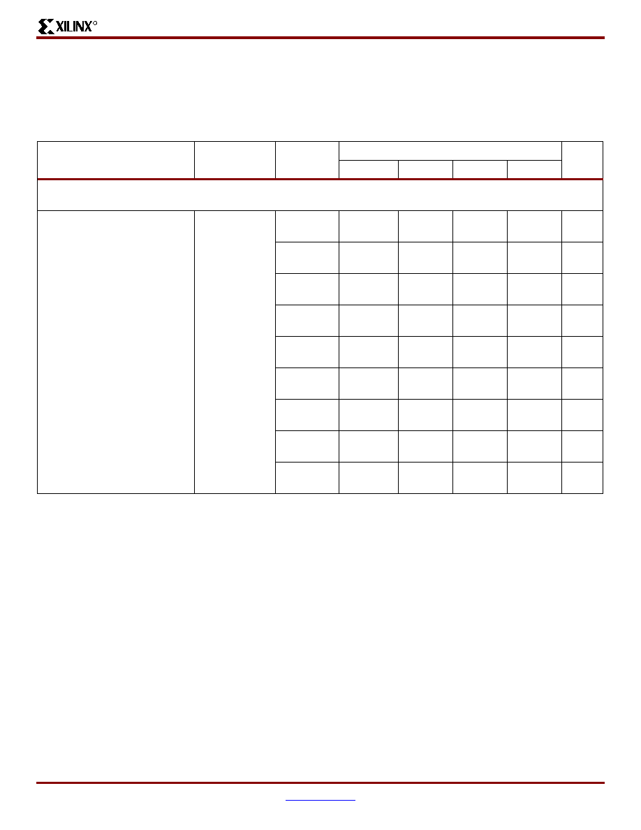
VirtexTM 2.5 V Field Programmable Gate Arrays
R
DS003-3 (v3.2) September 10, 2002
www.xilinx.com
Module 3 of 4
Production Product Specification
1-800-255-7778
19
Virtex Pin-to-Pin Input Parameter Guidelines
All devices are 100% functionally tested. Listed below are representative values for typical pin locations and normal clock
loading. Values are expressed in nanoseconds unless otherwise noted
Global Clock Set-Up and Hold for LVTTL Standard, with DLL
Description
Symbol
Device
Speed Grade
Units
Min
-6
-5
-4
Input Setup and Hold Time Relative to Global Clock Input Signal for LVTTL Standard. For data input with different
standards, adjust the setup time delay by the values shown in Input Delay Adjustments.
No Delay
Global Clock and IFF, with DLL
T
PSDLL
/T
PHDLL
XCV50
0.40 / ≠0.4
1.7 /≠0.4
1.8 /≠0.4
2.1 /≠0.4
ns,
min
XCV100
0.40 /≠0.4
1.7 /≠0.4
1.9 /≠0.4
2.1 /≠0.4
ns,
min
XCV150
0.40 /≠0.4
1.7 /≠0.4
1.9 /≠0.4
2.1 /≠0.4
ns,
min
XCV200
0.40 /≠0.4
1.7 /≠0.4
1.9 /≠0.4
2.1 /≠0.4
ns,
min
XCV300
0.40 /≠0.4
1.7 /≠0.4
1.9 /≠0.4
2.1 /≠0.4
ns,
min
XCV400
0.40 /≠0.4
1.7 /≠0.4
1.9 /≠0.4
2.1 /≠0.4
ns,
min
XCV600
0.40 /≠0.4
1.7 /≠0.4
1.9 /≠0.4
2.1 /≠0.4
ns,
min
XCV800
0.40 /≠0.4
1.7 /≠0.4
1.9 /≠0.4
2.1 /≠0.4
ns,
min
XCV1000
0.40 /≠0.4
1.7 /≠0.4
1.9 /≠0.4
2.1 /≠0.4
ns,
min
IFF = Input Flip-Flop or Latch
Notes:
1.
Set-up time is measured relative to the Global Clock input signal with the fastest route and the lightest load. Hold time is measured
relative to the Global Clock input signal with the slowest route and heaviest load.
2.
DLL output jitter is already included in the timing calculation.
3.
A Zero "0" Hold Time listing indicates no hold time or a negative hold time. Negative values can not be guaranteed "best-case", but
if a "0" is listed, there is no positive hold time.
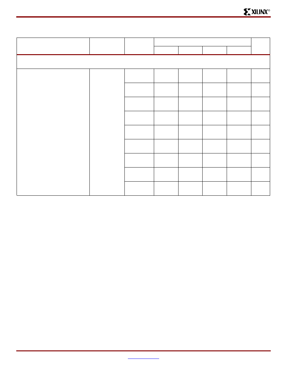
VirtexTM 2.5 V Field Programmable Gate Arrays
R
Module 3 of 4
www.xilinx.com
DS003-3 (v3.2) September 10, 2002
20
1-800-255-7778
Production Product Specification
Global Clock Set-Up and Hold for LVTTL Standard, without DLL
Description
Symbol
Device
Speed Grade
Units
Min
-6
-5
-4
Input Setup and Hold Time Relative to Global Clock Input Signal for LVTTL Standard.
(2)
For data input with different
standards, adjust the setup time delay by the values shown in Input Delay Adjustments.
Full Delay
Global Clock and IFF, without
DLL
T
PSFD
/T
PHFD
XCV50
0.6 / 0
2.3 / 0
2.6 / 0
2.9 / 0
ns,
min
XCV100
0.6 / 0
2.3 / 0
2.6 / 0
3.0 / 0
ns,
min
XCV150
0.6 / 0
2.4 / 0
2.7 / 0
3.1 / 0
ns,
min
XCV200
0.7 / 0
2.5 / 0
2.8 / 0
3.2 / 0
ns,
min
XCV300
0.7 / 0
2.5 / 0
2.8 / 0
3.2 / 0
ns,
min
XCV400
0.7 / 0
2.6 / 0
2.9 / 0
3.3 / 0
ns,
min
XCV600
0.7 / 0
2.6 / 0
2.9 / 0
3.3 / 0
ns,
min
XCV800
0.7 / 0
2.7 / 0
3.1 / 0
3.5 / 0
ns,
min
XCV1000
0.7 / 0
2.8 / 0
3.1 / 0
3.6 / 0
ns,
min
IFF = Input Flip-Flop or Latch
Notes: Notes:
1.
Set-up time is measured relative to the Global Clock input signal with the fastest route and the lightest load. Hold time is measured
relative to the Global Clock input signal with the slowest route and heaviest load.
2.
A Zero "0" Hold Time listing indicates no hold time or a negative hold time. Negative values can not be guaranteed "best-case", but
if a "0" is listed, there is no positive hold time.

VirtexTM 2.5 V Field Programmable Gate Arrays
R
DS003-3 (v3.2) September 10, 2002
www.xilinx.com
Module 3 of 4
Production Product Specification
1-800-255-7778
21
DLL Timing Parameters
All devices are 100 percent functionally tested. Because of the difficulty in directly measuring many internal timing
parameters, those parameters are derived from benchmark timing patterns. The following guidelines reflect worst-case
values across the recommended operating conditions.
DLL Clock Tolerance, Jitter, and Phase Information
All DLL output jitter and phase specifications determined through statistical measurement at the package pins using a clock
mirror configuration and matched drivers.
Description
Symbol
Speed Grade
Units
-6
-5
-4
Min
Max
Min
Max
Min
Max
Input Clock Frequency (CLKDLLHF)
FCLKINHF
60
200
60
180
60
180
MHz
Input Clock Frequency (CLKDLL)
FCLKINLF
25
100
25
90
25
90
MHz
Input Clock Pulse Width (CLKDLLHF)
T
DLLPWHF
2.0
-
2.4
-
2.4
-
ns
Input Clock Pulse Width (CLKDLL)
T
DLLPWLF
2.5
-
3.0
3.0
-
ns
Notes:
1.
All specifications correspond to Commercial Operating Temperatures (0∞C to + 85∞C).
Description
Symbol
F
CLKIN
CLKDLLHF
CLKDLL
Units
Min
Max
Min
Max
Input Clock Period Tolerance
T
IPTOL
-
1.0
-
1.0
ns
Input Clock Jitter Tolerance (Cycle to Cycle)
T
IJITCC
-
± 150
-
± 300
ps
Time Required for DLL to Acquire Lock
T
LOCK
> 60 MHz
-
20
-
20
µs
50 - 60 MHz
-
-
-
25
µs
40 - 50 MHz
-
-
-
50
µs
30 - 40 MHz
-
-
-
90
µs
25 - 30 MHz
-
-
-
120
µs
Output Jitter (cycle-to-cycle) for any DLL Clock Output
(1)
T
OJITCC
± 60
± 60
ps
Phase Offset between CLKIN and CLKO
(2)
T
PHIO
± 100
± 100
ps
Phase Offset between Clock Outputs on the DLL
(3)
T
PHOO
± 140
± 140
ps
Maximum Phase Difference between CLKIN and
CLKO
(4)
T
PHIOM
± 160
± 160
ps
Maximum Phase Difference between Clock Outputs on
the DLL
(5)
T
PHOOM
± 200
± 200
ps
Notes:
1.
Output Jitter is cycle-to-cycle jitter measured on the DLL output clock, excluding input clock jitter.
2.
Phase Offset between CLKIN and CLKO is the worst-case fixed time difference between rising edges of CLKIN and CLKO,
excluding Output Jitter and input clock jitter.
3.
Phase Offset between Clock Outputs on the DLL is the worst-case fixed time difference between rising edges of any two DLL
outputs, excluding Output Jitter and input clock jitter.
4.
Maximum Phase Difference between CLKIN an CLKO is the sum of Output Jitter and Phase Offset between CLKIN and CLKO,
or the greatest difference between CLKIN and CLKO rising edges due to DLL alone (excluding input clock jitter).
5.
Maximum Phase DIfference between Clock Outputs on the DLL is the sum of Output JItter and Phase Offset between any DLL
clock outputs, or the greatest difference between any two DLL output rising edges sue to DLL alone (excluding input clock jitter).
6.
All specifications correspond to Commercial Operating Temperatures (0∞C to +85∞C).

VirtexTM 2.5 V Field Programmable Gate Arrays
R
Module 3 of 4
www.xilinx.com
DS003-3 (v3.2) September 10, 2002
22
1-800-255-7778
Production Product Specification
Revision History
Figure 1: Frequency Tolerance and Clock Jitter
Date
Version
Revision
11/98
1.0
Initial Xilinx release.
01/99
1.2
Updated package drawings and specs.
02/99
1.3
Update of package drawings, updated specifications.
05/99
1.4
Addition of package drawings and specifications.
05/99
1.5
Replaced FG 676 & FG680 package drawings.
07/99
1.6
Changed Boundary Scan Information and changed Figure 11, Boundary Scan Bit
Sequence. Updated IOB Input & Output delays. Added Capacitance info for different I/O
Standards. Added 5 V tolerant information. Added DLL Parameters and waveforms and
new Pin-to-pin Input and Output Parameter tables for Global Clock Input to Output and
Setup and Hold. Changed Configuration Information including Figures 12, 14, 17 & 19.
Added device-dependent listings for quiescent currents ICCINTQ and ICCOQ. Updated
IOB Input and Output Delays based on default standard of LVTTL, 12 mA, Fast Slew Rate.
Added IOB Input Switching Characteristics Standard Adjustments.
09/99
1.7
Speed grade update to preliminary status, Power-on specification and Clock-to-Out
Minimums additions, "0" hold time listing explanation, quiescent current listing update, and
Figure 6 ADDRA input label correction. Added T
IJITCC
parameter, changed T
OJIT
to T
OPHASE
.
01/00
1.8
Update to speed.txt file 1.96. Corrections for CRs 111036,111137, 112697, 115479,
117153, 117154, and 117612. Modified notes for Recommended Operating Conditions
(voltage and temperature). Changed Bank information for V
CCO
in CS144 package on p.43.
TCLKIN
TCLKIN + TIPTOL
Period Tolerance: the allowed input clock period change in nanoseconds.
Output Jitter: the difference between an ideal
reference clock edge and the actual design.
_
ds003_20c_110399
Ideal Period
Actual Period
+ Jitter
+/- Jitter
+ Maximum
Phase Difference
Phase Offset and Maximum Phase Difference
+ Phase Offset
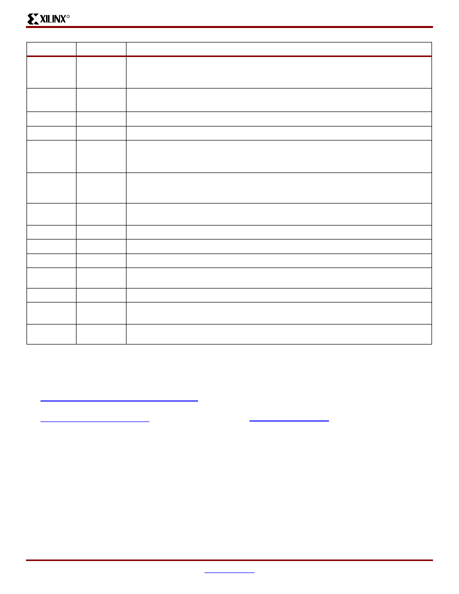
VirtexTM 2.5 V Field Programmable Gate Arrays
R
DS003-3 (v3.2) September 10, 2002
www.xilinx.com
Module 3 of 4
Production Product Specification
1-800-255-7778
23
Virtex Data Sheet
The Virtex Data Sheet contains the following modules:
∑
DS003-1, Virtex 2.5V FPGAs:
Introduction and Ordering Information (Module 1)
∑
DS003-2, Virtex 2.5V FPGAs:
Functional Description (Module 2)
∑
DS003-3, Virtex 2.5V FPGAs:
DC and Switching Characteristics (Module 3)
∑
DS003-4, Virtex 2.5V FPGAs:
Pinout Tables (Module 4)
01/00
1.9
Updated DLL Jitter Parameter table and waveforms, added Delay Measurement
Methodology table for different I/O standards, changed buffered Hex line info and
Input/Output Timing measurement notes.
03/00
2.0
New TBCKO values; corrected FG680 package connection drawing; new note about status
of CCLK pin after configuration.
05/00
2.1
Modified "Pins not listed ..." statement. Speed grade update to Final status.
05/00
2.2
Modified Table 18.
09/00
2.3
∑
Added XCV400 values to table under Minimum Clock-to-Out for Virtex Devices.
∑
Corrected Units column in table under IOB Input Switching Characteristics.
∑
Added values to table under CLB SelectRAM Switching Characteristics.
10/00
2.4
∑
Corrected Pinout information for devices in the BG256, BG432, and BG560 packages in
Table 18.
∑
Corrected BG256 Pin Function Diagram.
04/02/01
2.5
∑
Revised minimums for Global Clock Set-Up and Hold for LVTTL Standard, with DLL.
∑
Converted file to modularized format. See the
Virtex Data Sheet
section.
04/19/01
2.6
∑
Clarified
TIOCKP
and
TIOCKON
IOB Output Switching Characteristics
descriptors.
07/19/01
2.7
∑
Under
Absolute Maximum Ratings
, changed (T
SOL
) to 220
∞C .
07/26/01
2.8
∑
Removed T
SOL
parameter and added footnote to
Absolute Maximum Ratings
table.
10/29/01
2.9
∑
Updated the speed grade designations used in data sheets, and added
Table 1
, which
shows the current speed grade designation for each device.
02/01/02
3.0
∑
Added footnote to
DC Input and Output Levels
table.
07/19/02
3.1
∑
Removed mention of MIL-M-38510/605 specification.
∑
Added link to xapp158 from the
Power-On Power Supply Requirements
section.
09/10/02
3.2
∑
Added Clock CLK to
IOB Input Switching Characteristics
and
IOB Output Switching
Characteristics
.
Date
Version
Revision

VirtexTM 2.5 V Field Programmable Gate Arrays
R
Module 3 of 4
www.xilinx.com
DS003-3 (v3.2) September 10, 2002
24
1-800-255-7778
Production Product Specification
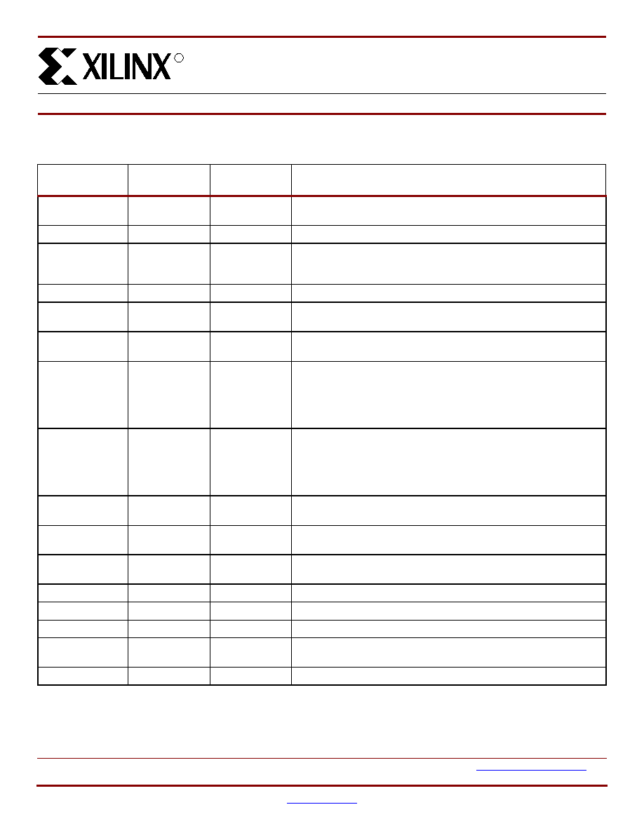
© 1999-2002 Xilinx, Inc. All rights reserved. All Xilinx trademarks, registered trademarks, patents, and disclaimers are as listed at
http://www.xilinx.com/legal.htm
.
All other trademarks and registered trademarks are the property of their respective owners. All specifications are subject to change without notice.
DS003-4 (v2.8) July 19, 2002
www.xilinx.com
Module 4 of 4
Production Product Specification
1-800-255-7778
1
Virtex Pin Definitions
0
VirtexTM 2.5 V
Field Programmable Gate Arrays
DS003-4 (v2.8) July 19, 2002
0
0
Production Product Specification
Table 1: Special Purpose Pins
Pin Name
Dedicated
Pin
Direction
Description
GCK0, GCK1,
GCK2, GCK3
Yes
Input
Clock input pins that connect to Global Clock Buffers. These pins become
user inputs when not needed for clocks.
M0, M1, M2
Yes
Input
Mode pins are used to specify the configuration mode.
CCLK
Yes
Input or
Output
The configuration Clock I/O pin: it is an input for SelectMAP and
slave-serial modes, and output in master-serial mode. After configuration,
it is input only, logic level = Don't Care.
PROGRAM
Yes
Input
Initiates a configuration sequence when asserted Low.
DONE
Yes
Bidirectional
Indicates that configuration loading is complete, and that the start-up
sequence is in progress. The output can be open drain.
INIT
No
Bidirectional
(Open-drain)
When Low, indicates that the configuration memory is being cleared. The
pin becomes a user I/O after configuration.
BUSY/
DOUT
No
Output
In SelectMAP mode, BUSY controls the rate at which configuration data
is loaded. The pin becomes a user I/O after configuration unless the
SelectMAP port is retained.
In bit-serial modes, DOUT provides header information to downstream
devices in a daisy-chain. The pin becomes a user I/O after configuration.
D0/DIN,
D1, D2,
D3, D4,
D5, D6,
D7
No
Input or
Output
In SelectMAP mode, D0 - D7 are configuration data pins. These pins
become user I/Os after configuration unless the SelectMAP port is
retained.
In bit-serial modes, DIN is the single data input. This pin becomes a user
I/O after configuration.
WRITE
No
Input
In SelectMAP mode, the active-low Write Enable signal. The pin becomes
a user I/O after configuration unless the SelectMAP port is retained.
CS
No
Input
In SelectMAP mode, the active-low Chip Select signal. The pin becomes
a user I/O after configuration unless the SelectMAP port is retained.
TDI, TDO,
TMS, TCK
Yes
Mixed
Boundary-scan Test-Access-Port pins, as defined in IEEE 1149.1.
DXN, DXP
Yes
N/A
Temperature-sensing diode pins. (Anode: DXP, cathode: DXN)
V
CCINT
Yes
Input
Power-supply pins for the internal core logic.
V
CCO
Yes
Input
Power-supply pins for the output drivers (subject to banking rules)
V
REF
No
Input
Input threshold voltage pins. Become user I/Os when an external
threshold voltage is not needed (subject to banking rules).
GND
Yes
Input
Ground
R

VirtexTM 2.5 V Field Programmable Gate Arrays
R
Module 4 of 4
www.xilinx.com
DS003-4 (v2.8) July 19, 2002
2
1-800-255-7778
Production Product Specification
Virtex Pinout Information
Pinout Tables
See
www.xilinx.com
for updates or additional pinout information. For convenience,
Table 2
,
Table 3
and
Table 4
list the
locations of special-purpose and power-supply pins. Pins not listed are either user I/Os or not connected, depending on the
device/package combination. See the Pinout Diagrams starting on
page 17
for any pins not listed for a particular
part/package combination.
Table 2: Virtex Pinout Tables (Chip-Scale and QFP Packages)
Pin Name
Device
CS144
TQ144
PQ/HQ240
GCK0
All
K7
90
92
GCK1
All
M7
93
89
GCK2
All
A7
19
210
GCK3
All
A6
16
213
M0
All
M1
110
60
M1
All
L2
112
58
M2
All
N2
108
62
CCLK
All
B13
38
179
PROGRAM
All
L12
72
122
DONE
All
M12
74
120
INIT
All
L13
71
123
BUSY/DOUT
All
C11
39
178
D0/DIN
All
C12
40
177
D1
All
E10
45
167
D2
All
E12
47
163
D3
All
F11
51
156
D4
All
H12
59
145
D5
All
J13
63
138
D6
All
J11
65
134
D7
All
K10
70
124
WRITE
All
C10
32
185
CS
All
D10
33
184
TDI
All
A11
34
183
TDO
All
A12
36
181
TMS
All
B1
143
2
TCK
All
C3
2
239
V
CCINT
All
A9, B6, C5, G3,
G12, M5, M9, N6
10, 15, 25, 57, 84, 94,
99, 126
16, 32, 43, 77, 88, 104,
137, 148, 164, 198,
214, 225
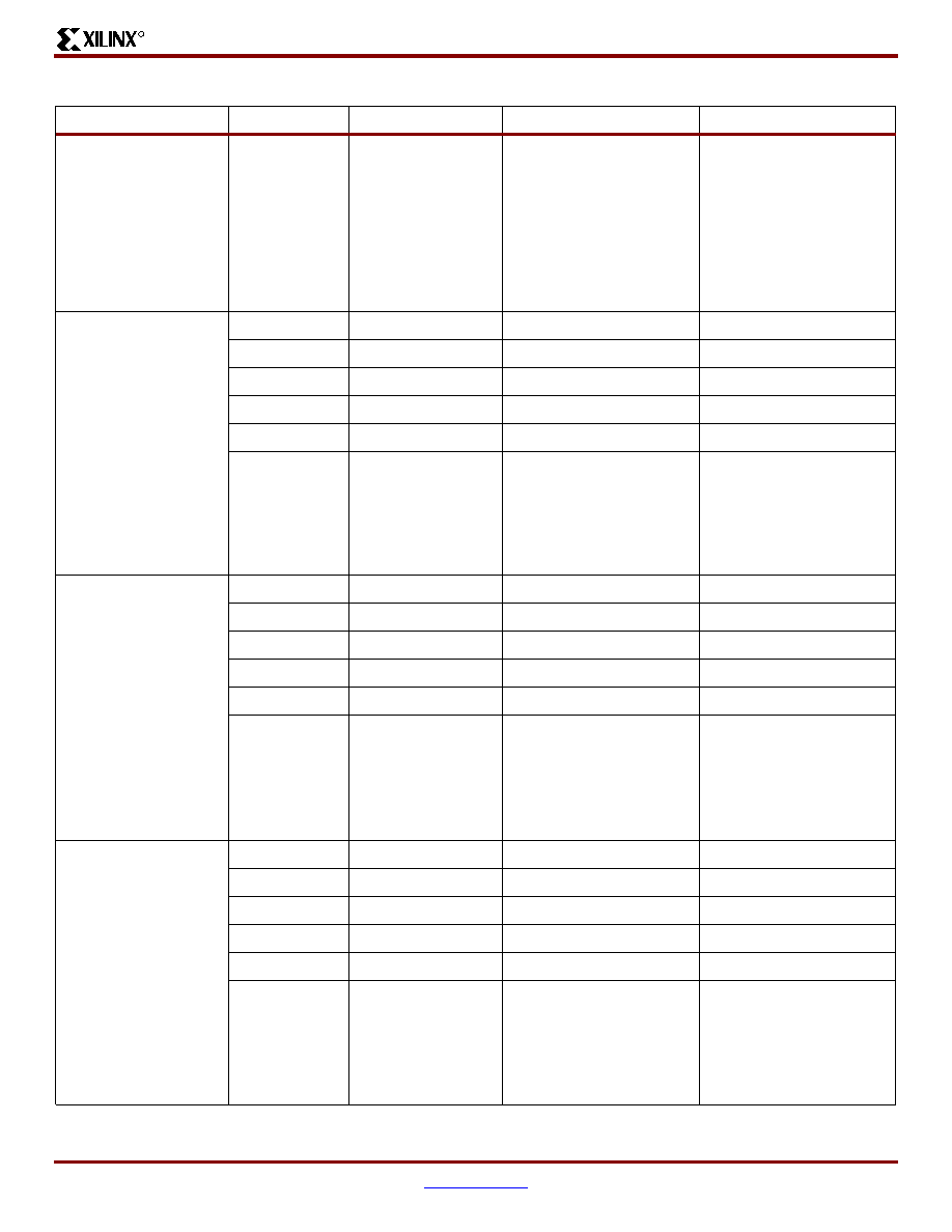
VirtexTM 2.5 V Field Programmable Gate Arrays
R
DS003-4 (v2.8) July 19, 2002
www.xilinx.com
Module 4 of 4
Production Product Specification
1-800-255-7778
3
V
CCO
All
Banks 0 and 1:
A2, A13, D7
Banks 2 and 3:
B12, G11, M13
Banks 4 and 5:
N1, N7, N13
Banks 6 and 7:
B2, G2, M2
No I/O Banks in this
package:
1, 17, 37, 55, 73, 92,
109, 128
No I/O Banks in this
package:
15, 30, 44, 61, 76, 90,
105, 121, 136, 150, 165,
180, 197, 212, 226, 240
V
REF
, Bank 0
(V
REF
pins are listed
incrementally. Connect
all pins listed for both
the required device
and all smaller devices
listed in the same
package.)
Within each bank, if
input reference voltage
is not required, all
V
REF
pins are general
I/O.
XCV50
C4, D6
5, 13
218, 232
XCV100/150
... + B4
... + 7
... + 229
XCV200/300
N/A
N/A
... + 236
XCV400
N/A
N/A
... + 215
XCV600
N/A
N/A
... + 230
XCV800
N/A
N/A
... + 222
V
REF
, Bank 1
(V
REF
pins are listed
incrementally. Connect
all pins listed for both
the required device
and all smaller devices
listed in the same
package.)
Within each bank, if
input reference voltage
is not required, all
V
REF
pins are general
I/O.
XCV50
A10, B8
22, 30
191, 205
XCV100/150
... + D9
... + 28
... + 194
XCV200/300
N/A
N/A
... + 187
XCV400
N/A
N/A
... + 208
XCV600
N/A
N/A
... + 193
XCV800
N/A
N/A
... + 201
V
REF
, Bank 2
(V
REF
pins are listed
incrementally. Connect
all pins listed for both
the required device
and all smaller devices
listed in the same
package.)
Within each bank, if
input reference voltage
is not required, all
V
REF
pins are general
I/O.
XCV50
D11, F10
42, 50
157, 171
XCV100/150
... + D13
... + 44
... + 168
XCV200/300
N/A
N/A
... + 175
XCV400
N/A
N/A
... + 154
XCV600
N/A
N/A
... + 169
XCV800
N/A
N/A
... + 161
Table 2: Virtex Pinout Tables (Chip-Scale and QFP Packages) (Continued)
Pin Name
Device
CS144
TQ144
PQ/HQ240
VirtexTM 2.5 V Field Programmable Gate Arrays
R
Module 4 of 4
www.xilinx.com
DS003-4 (v2.8) July 19, 2002
4
1-800-255-7778
Production Product Specification
V
REF
, Bank 3
(V
REF
pins are listed
incrementally. Connect
all pins listed for both
the required device
and all smaller devices
listed in the same
package.)
Within each bank, if
input reference voltage
is not required, all
V
REF
pins are general
I/O.
XCV50
H11, K12
60, 68
130, 144
XCV100/150
... + J10
... + 66
... + 133
XCV200/300
N/A
N/A
... + 126
XCV400
N/A
N/A
... + 147
XCV600
N/A
N/A
... + 132
XCV800
N/A
N/A
... + 140
V
REF
, Bank 4
(V
REF
pins are listed
incrementally. Connect
all pins listed for both
the required device
and all smaller devices
listed in the same
package.)
Within each bank, if
input reference voltage
is not required, all
V
REF
pins are general
I/O.
XCV50
L8, L10
79, 87
97, 111
XCV100/150
... + N10
... + 81
... + 108
XCV200/300
N/A
N/A
... + 115
XCV400
N/A
N/A
... + 94
XCV600
N/A
N/A
... + 109
XCV800
N/A
N/A
... + 101
V
REF
, Bank 5
(V
REF
pins are listed
incrementally. Connect
all pins listed for both
the required device
and all smaller devices
listed in the same
package.)
Within each bank, if
input reference voltage
is not required, all
V
REF
pins are general
I/O.
XCV50
L4, L6
96, 104
70, 84
XCV100/150
... + N4
... + 102
... + 73
XCV200/300
N/A
N/A
... + 66
XCV400
N/A
N/A
... + 87
XCV600
N/A
N/A
... + 72
XCV800
N/A
N/A
... + 80
Table 2: Virtex Pinout Tables (Chip-Scale and QFP Packages) (Continued)
Pin Name
Device
CS144
TQ144
PQ/HQ240
VirtexTM 2.5 V Field Programmable Gate Arrays
R
DS003-4 (v2.8) July 19, 2002
www.xilinx.com
Module 4 of 4
Production Product Specification
1-800-255-7778
5
V
REF
, Bank 6
(V
REF
pins are listed
incrementally. Connect
all pins listed for both
the required device
and all smaller devices
listed in the same
package.)
Within each bank, if
input reference voltage
is not required, all
V
REF
pins are general
I/O.
XCV50
H2, K1
116, 123
36, 50
XCV100/150
... + J3
... + 118
... + 47
XCV200/300
N/A
N/A
... + 54
XCV400
N/A
N/A
... + 33
XCV600
N/A
N/A
... + 48
XCV800
N/A
N/A
... + 40
V
REF
, Bank 7
(V
REF
pins are listed
incrementally. Connect
all pins listed for both
the required device
and all smaller devices
listed in the same
package.)
Within each bank, if
input reference voltage
is not required, all
V
REF
pins are general
I/O.
XCV50
D4, E1
133, 140
9, 23
XCV100/150
... + D2
... + 138
... + 12
XCV200/300
N/A
N/A
... + 5
XCV400
N/A
N/A
... + 26
XCV600
N/A
N/A
... + 11
XCV800
N/A
N/A
... + 19
GND
All
A1, B9, B11, C7,
D5, E4, E11, F1,
G10, J1, J12, L3,
L5, L7, L9, N12
9, 18, 26, 35, 46, 54, 64,
75, 83, 91, 100, 111, 120,
129, 136, 144,
1, 8, 14, 22, 29, 37, 45, 51,
59, 69, 75, 83, 91, 98, 106,
112, 119, 129, 135, 143,
151, 158, 166, 172, 182,
190, 196, 204, 211, 219,
227, 233
Table 2: Virtex Pinout Tables (Chip-Scale and QFP Packages) (Continued)
Pin Name
Device
CS144
TQ144
PQ/HQ240
VirtexTM 2.5 V Field Programmable Gate Arrays
R
Module 4 of 4
www.xilinx.com
DS003-4 (v2.8) July 19, 2002
6
1-800-255-7778
Production Product Specification
Table 3: Virtex Pinout Tables (BGA)
Pin Name
Device
BG256
BG352
BG432
BG560
GCK0
All
Y11
AE13
AL16
AL17
GCK1
All
Y10
AF14
AK16
AJ17
GCK2
All
A10
B14
A16
D17
GCK3
All
B10
D14
D17
A17
M0
All
Y1
AD24
AH28
AJ29
M1
All
U3
AB23
AH29
AK30
M2
All
W2
AC23
AJ28
AN32
CCLK
All
B19
C3
D4
C4
PROGRAM
All
Y20
AC4
AH3
AM1
DONE
All
W19
AD3
AH4
AJ5
INIT
All
U18
AD2
AJ2
AH5
BUSY/DOUT
All
D18
E4
D3
D4
D0/DIN
All
C19
D3
C2
E4
D1
All
E20
G1
K4
K3
D2
All
G19
J3
K2
L4
D3
All
J19
M3
P4
P3
D4
All
M19
R3
V4
W4
D5
All
P19
U4
AB1
AB5
D6
All
T20
V3
AB3
AC4
D7
All
V19
AC3
AG4
AJ4
WRITE
All
A19
D5
B4
D6
CS
All
B18
C4
D5
A2
TDI
All
C17
B3
B3
D5
TDO
All
A20
D4
C4
E6
TMS
All
D3
D23
D29
B33
TCK
All
A1
C24
D28
E29
DXN
All
W3
AD23
AH27
AK29
DXP
All
V4
AE24
AK29
AJ28
VirtexTM 2.5 V Field Programmable Gate Arrays
R
DS003-4 (v2.8) July 19, 2002
www.xilinx.com
Module 4 of 4
Production Product Specification
1-800-255-7778
7
V
CCINT
Notes:
∑ Superset includes all pins,
including the ones in bold
type. Subset excludes pins in
bold type.
∑ In BG352, for XCV300 all the
V
CCINT
pins in the superset
must be connected. For
XCV150/200, V
CCINT
pins in
the subset must be
connected, and pins in bold
type can be left unconnected
(these unconnected pins
cannot be used as user I/O.)
∑ In BG432, for
XCV400/600/800 all V
CCINT
pins in the superset must be
connected. For XCV300,
V
CCINT
pins in the subset
must be connected, and pins
in bold type can be left
unconnected (these
unconnected pins cannot be
used as user I/O.)
∑ In BG560, for XCV800/1000
all V
CCINT
pins in the
superset must be connected.
For XCV400/600, V
CCINT
pins in the subset must be
connected, and pins in bold
type can be left unconnected
(these unconnected pins
cannot be used as user I/O.)
XCV50/100
C10, D6,
D15, F4,
F17, L3,
L18, R4,
R17, U6,
U15, V10
N/A
N/A
N/A
XCV150/200/300
Same as
above
A20, C14,
D10, J24,
K4, P2, P25,
V24, W2,
AC10, AE14,
AE19,
B16, D12,
L1, L25,
R23, T1,
AF11, AF16
A10, A17, B23,
C14, C19, K3,
K29, N2, N29,
T1, T29, W2,
W31, AB2,
AB30, AJ10,
AJ16, AK13,
AK19, AK22,
B26, C7, F1,
F30, AE29, AF1,
AH8, AH24
N/A
XCV400/600/800/1000
N/A
N/A
Same as above
A21, B14, B18,
B28, C24, E9,
E12, F2, H30,
J1, K32, N1,
N33, U5, U30,
Y2, Y31, AD2,
AD32, AG3,
AG31, AK8,
AK11, AK17,
AK20, AL14,
AL27, AN25,
B12, C22, M3,
N29, AB2,
AB32, AJ13,
AL22
V
CCO
, Bank 0
All
D7, D8
A17, B25,
D19
A21, C29, D21
A22, A26, A30,
B19, B32
V
CCO
, Bank 1
All
D13, D14
A10, D7,
D13
A1, A11, D11
A10, A16, B13,
C3, E5
V
CCO
, Bank 2
All
G17, H17
B2, H4, K1
C3, L1, L4
B2, D1, H1, M1,
R2
V
CCO
, Bank 3
All
N17, P17
P4, U1, Y4
AA1, AA4, AJ3
V1, AA2, AD1,
AK1, AL2
V
CCO
, Bank 4
All
U13, U14
AC8, AE2,
AF10
AH11, AL1,
AL11
AM2, AM15,
AN4, AN8, AN12
V
CCO
, Bank 5
All
U7, U8
AC14, AC20,
AF17
AH21, AJ29,
AL21
AL31, AM21,
AN18, AN24,
AN30
V
CCO
, Bank 6
All
N4, P4
U26, W23,
AE25
AA28, AA31,
AL31
W32, AB33,
AF33, AK33,
AM32
Table 3: Virtex Pinout Tables (BGA) (Continued)
Pin Name
Device
BG256
BG352
BG432
BG560
VirtexTM 2.5 V Field Programmable Gate Arrays
R
Module 4 of 4
www.xilinx.com
DS003-4 (v2.8) July 19, 2002
8
1-800-255-7778
Production Product Specification
V
CCO
, Bank 7
All
G4, H4
G23, K26,
N23
A31, L28, L31
C32, D33, K33,
N32, T33
V
REF
, Bank 0
(VREF pins are listed
incrementally. Connect all
pins listed for both the
required device and all
smaller devices listed in the
same package.)
Within each bank, if input
reference voltage is not
required, all V
REF
pins are
general I/O.
XCV50
A8, B4
N/A
N/A
N/A
XCV100/150
... + A4
A16,C19,
C21
N/A
N/A
XCV200/300
... + A2
... + D21
B19, D22, D24,
D26
N/A
XCV400
N/A
N/A
... + C18
A19, D20,
D26, E23, E27
XCV600
N/A
N/A
... + C24
... + E24
XCV800
N/A
N/A
... + B21
... + E21
XCV1000
N/A
N/A
N/A
... + D29
V
REF
, Bank 1
(VREF pins are listed
incrementally. Connect all
pins listed for both the
required device and all
smaller devices listed in the
same package.)
Within each bank, if input
reference voltage is not
required, all V
REF
pins are
general I/O.
XCV50
A17, B12
N/A
N/A
N/A
XCV100/150
... + B15
B6, C9,
C12
N/A
N/A
XCV200/300
... + B17
... + D6
A13, B7,
C6, C10
N/A
XCV400
N/A
N/A
... + B15
A6, D7,
D11, D16, E15
XCV600
N/A
N/A
... + D10
... + D10
XCV800
N/A
N/A
... + B12
... + D13
XCV1000
N/A
N/A
N/A
... + E7
V
REF
, Bank 2
(V
REF
pins are listed
incrementally. Connect all
pins listed for both the
required device and all
smaller devices listed in the
same package.)
Within each bank, if input
reference voltage is not
required, all V
REF
pins are
general I/O.
XCV50
C20, J18
N/A
N/A
N/A
XCV100/150
... + F19
E2, H2,
M4
N/A
N/A
XCV200/300
... + G18
... + D2
E2, G3,
J2, N1
N/A
XCV400
N/A
N/A
... + R3
G5, H4,
L5, P4, R1
XCV600
N/A
N/A
... + H1
... + K5
XCV800
N/A
N/A
... + M3
... + N5
XCV1000
N/A
N/A
N/A
... + B3
Table 3: Virtex Pinout Tables (BGA) (Continued)
Pin Name
Device
BG256
BG352
BG432
BG560
VirtexTM 2.5 V Field Programmable Gate Arrays
R
DS003-4 (v2.8) July 19, 2002
www.xilinx.com
Module 4 of 4
Production Product Specification
1-800-255-7778
9
V
REF
, Bank 3
(V
REF
pins are listed
incrementally. Connect all
pins listed for both the
required device and all
smaller devices listed in the
same package.)
Within each bank, if input
reference voltage is not
required, all V
REF
pins are
general I/O.
XCV50
M18, V20
N/A
N/A
N/A
XCV100/150
... + R19
R4, V4, Y3
N/A
N/A
XCV200/300
... + P18
... + AC2
V2, AB4, AD4,
AF3
N/A
XCV400
N/A
N/A
... + U2
V4, W5,
AD3, AE5, AK2
XCV600
N/A
N/A
... + AC3
... + AF1
XCV800
N/A
N/A
... + Y3
... + AA4
XCV1000
N/A
N/A
N/A
... + AH4
V
REF
, Bank 4
(V
REF
pins are listed
incrementally. Connect all
pins listed for both the
required device and all
smaller devices listed in the
same package.)
Within each bank, if input
reference voltage is not
required, all V
REF
pins are
general I/O.
XCV50
V12, Y18
N/A
N/A
N/A
XCV100/150
... + W15
AC12, AE5,
AE8,
N/A
N/A
XCV200/300
... + V14
... + AE4
AJ7, AL4, AL8,
AL13
N/A
XCV400
N/A
N/A
... + AK15
AL7, AL10,
AL16, AM4,
AM14
XCV600
N/A
N/A
... + AK8
... + AL9
XCV800
N/A
N/A
... + AJ12
... + AK13
XCV1000
N/A
N/A
N/A
... + AN3
V
REF
, Bank 5
(V
REF
pins are listed
incrementally. Connect all
pins listed for both the
required device and all
smaller devices listed in the
same package.)
Within each bank, if input
reference voltage is not
required, all V
REF
pins are
general I/O.
XCV50
V9, Y3
N/A
N/A
N/A
XCV100/150
... + W6
AC15, AC18,
AD20
N/A
N/A
XCV200/300
... + V7
... + AE23
AJ18, AJ25,
AK23, AK27
N/A
XCV400
N/A
N/A
... + AJ17
AJ18, AJ25,
AL20, AL24,
AL29
XCV600
N/A
N/A
... + AL24
... + AM26
XCV800
N/A
N/A
... + AH19
... + AN23
XCV1000
N/A
N/A
N/A
... + AK28
V
REF
, Bank 6
(V
REF
pins are listed
incrementally. Connect all
pins listed for both the
required device and all
smaller devices listed in the
same package.)
Within each bank, if input
reference voltage is not
required, all V
REF
pins are
general I/O.
XCV50
M2, R3
N/A
N/A
N/A
XCV100/150
... + T1
R24, Y26,
AA25,
N/A
N/A
XCV200/300
... + T3
... + AD26
V28, AB28,
AE30, AF28
N/A
XCV400
N/A
N/A
... + U28
V29, Y32, AD31,
AE29, AK32
XCV600
N/A
N/A
... + AC28
... + AE31
XCV800
N/A
N/A
... + Y30
... + AA30
XCV1000
N/A
N/A
N/A
... + AH30
Table 3: Virtex Pinout Tables (BGA) (Continued)
Pin Name
Device
BG256
BG352
BG432
BG560
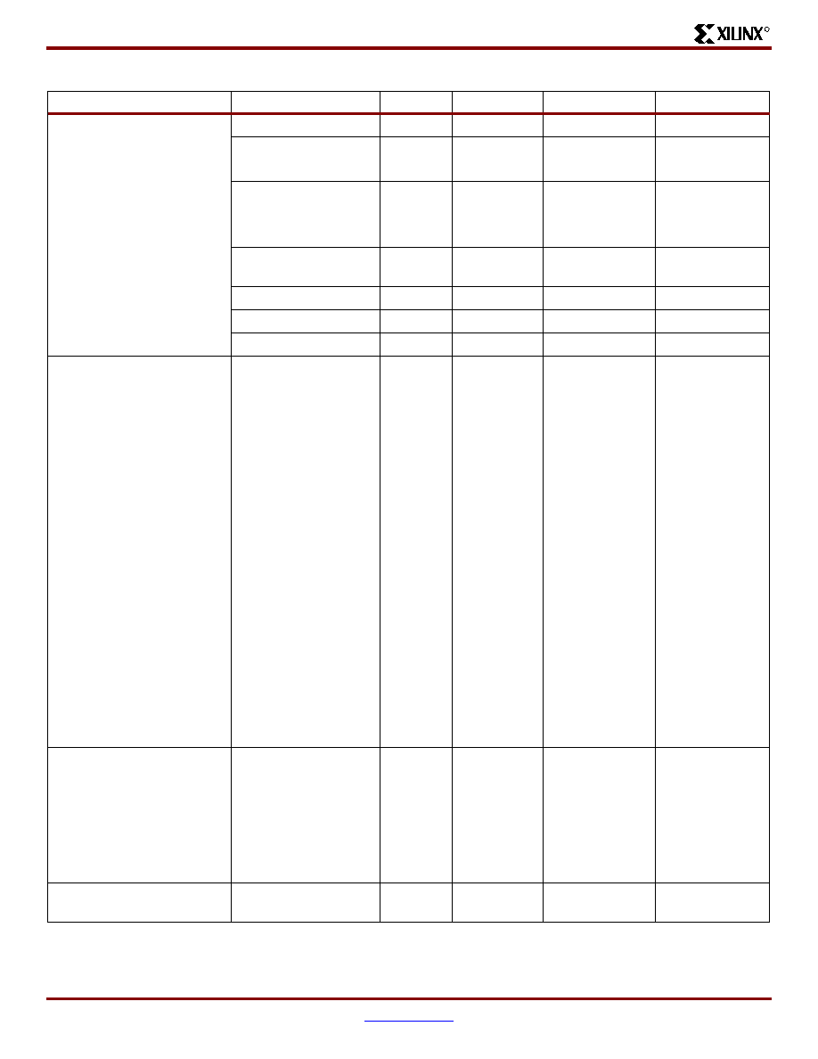
VirtexTM 2.5 V Field Programmable Gate Arrays
R
Module 4 of 4
www.xilinx.com
DS003-4 (v2.8) July 19, 2002
10
1-800-255-7778
Production Product Specification
V
REF
, Bank 7
(V
REF
pins are listed
incrementally. Connect all
pins listed for both the
required device and all
smaller devices listed in the
same package.)
Within each bank, if input
reference voltage is not
required, all V
REF
pins are
general I/O.
XCV50
G3, H1
N/A
N/A
N/A
XCV100/150
... + D1
D26, G26,
L26
N/A
N/A
XCV200/300
... + B2
... + E24
F28, F31,
J30, N30
N/A
XCV400
N/A
N/A
... + R31
E31, G31, K31,
P31, T31
XCV600
N/A
N/A
... + J28
... + H32
XCV800
N/A
N/A
... + M28
... + L33
XCV1000
N/A
N/A
N/A
... + D31
GND
All
C3, C18,
D4, D5,
D9, D10,
D11,
D12,
D16,
D17, E4,
E17, J4,
J17, K4,
K17, L4,
L17, M4,
M17, T4,
T17, U4,
U5, U9,
U10,
U11,
U12,
U16,
U17, V3,
V18
A1, A2, A5,
A8, A14,
A19, A22,
A25, A26,
B1, B26, E1,
E26, H1,
H26, N1,
P26, W1,
W26, AB1,
AB26, AE1,
AE26, AF1,
AF2, AF5,
AF8, AF13,
AF19, AF22,
AF25, AF26
A2, A3, A7, A9,
A14, A18, A23,
A25, A29, A30,
B1, B2, B30,
B31, C1, C31,
D16, G1, G31,
J1, J31, P1, P31,
T4, T28, V1,
V31, AC1, AC31,
AE1, AE31,
AH16, AJ1,
AJ31, AK1, AK2,
AK30, AK31,
AL2, AL3, AL7,
AL9 AL14, AL18
AL23, AL25,
AL29, AL30
A1, A7, A12,
A14, A18, A20,
A24, A29, A32,
A33, B1, B6, B9,
B15, B23, B27,
B31, C2, E1,
F32, G2, G33,
J32, K1, L2,
M33, P1, P33,
R32, T1, V33,
W2, Y1, Y33,
AB1, AC32,
AD33, AE2,
AG1, AG32,
AH2, AJ33,
AL32, AM3,
AM7, AM11,
AM19, AM25,
AM28, AM33,
AN1, AN2, AN5,
AN10, AN14,
AN16, AN20,
AN22, AN27,
AN33
GND
(1)
All
J9, J10,
J11, J12,
K9, K10,
K11, K12,
L9, L10,
L11, L12,
M9, M10,
M11, M12
N/A
N/A
N/A
No Connect
All
N/A
N/A
N/A
C31, AC2, AK4,
AL3
Notes:
1.
16 extra balls (grounded) at package center.
Table 3: Virtex Pinout Tables (BGA) (Continued)
Pin Name
Device
BG256
BG352
BG432
BG560
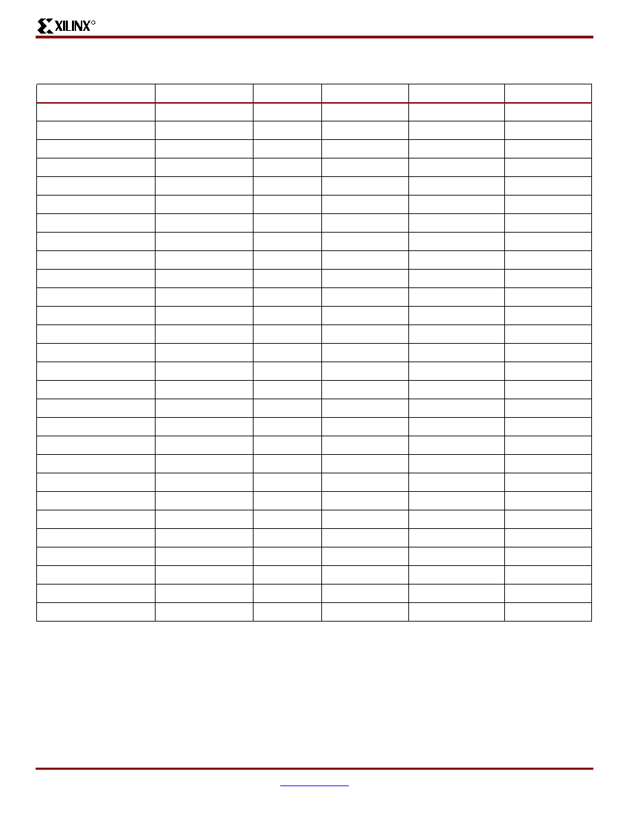
VirtexTM 2.5 V Field Programmable Gate Arrays
R
DS003-4 (v2.8) July 19, 2002
www.xilinx.com
Module 4 of 4
Production Product Specification
1-800-255-7778
11
Table 4: Virtex Pinout Tables (Fine-Pitch BGA)
Pin Name
Device
FG256
FG456
FG676
FG680
GCK0
All
N8
W12
AA14
AW19
GCK1
All
R8
Y11
AB13
AU22
GCK2
All
C9
A11
C13
D21
GCK3
All
B8
C11
E13
A20
M0
All
N3
AB2
AD4
AT37
M1
All
P2
U5
W7
AU38
M2
All
R3
Y4
AB6
AT35
CCLK
All
D15
B22
D24
E4
PROGRAM
All
P15
W20
AA22
AT5
DONE
All
R14
Y19
AB21
AU5
INIT
All
N15
V19
Y21
AU2
BUSY/DOUT
All
C15
C21
E23
E3
D0/DIN
All
D14
D20
F22
C2
D1
All
E16
H22
K24
P4
D2
All
F15
H20
K22
P3
D3
All
G16
K20
M22
R1
D4
All
J16
N22
R24
AD3
D5
All
M16
R21
U23
AG2
D6
All
N16
T22
V24
AH1
D7
All
N14
Y21
AB23
AR4
WRITE
All
C13
A20
C22
B4
CS
All
B13
C19
E21
D5
TDI
All
A15
B20
D22
B3
TDO
All
B14
A21
C23
C4
TMS
All
D3
D3
F5
E36
TCK
All
C4
C4
E6
C36
DXN
All
R4
Y5
AB7
AV37
DXP
All
P4
V6
Y8
AU35
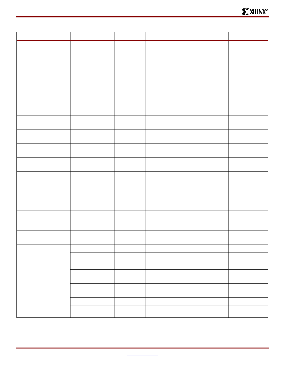
VirtexTM 2.5 V Field Programmable Gate Arrays
R
Module 4 of 4
www.xilinx.com
DS003-4 (v2.8) July 19, 2002
12
1-800-255-7778
Production Product Specification
V
CCINT
All
C3, C14, D4,
D13, E5,
E12, M5,
M12, N4,
N13, P3,
P14
E5, E18, F6,
F17, G7, G8, G9,
G14, G15, G16,
H7, H16, J7,
J16, P7, P16,
R7, R16, T7, T8,
T9, T14, T15,
T16, U6, U17,
V5, V18
G7, G20, H8, H19,
J9, J10, J11, J16,
J17, J18, K9, K18,
L9, L18, T9, T18,
U9, U18, V9, V10,
V11, V16, V17,
V18, W8, W19, Y7,
Y20
AD5, AD35,
AE5, AE35, AL5,
AL35, AM5,
AM35, AR8,
AR9, AR15,
AR16, AR24,
AR25, AR31,
AR32, E8, E9,
E15, E16, E24,
E25, E31, E32,
H5, H35, J5,
J35, R5, R35,
T5, T35
V
CCO
, Bank 0
All
E8, F8
F7, F8, F9, F10
G10, G11
H9, H10, H11,
H12, J12, J13
E26, E27, E29,
E30, E33, E34
V
CCO
, Bank 1
All
E9, F9
F13, F14, F15,
F16, G12, G13
H15, H16, H17,
H18, J14, J15
E6, E7, E10,
E11, E13, E14
V
CCO
, Bank 2
All
H11, H12
G17, H17, J17,
K16, K17, L16
J19, K19, L19,
M18, M19, N18
F5, G5, K5, L5,
N5, P5
V
CCO
, Bank 3
All
J11, J12
M16, N16, N17,
P17, R17, T17
P18, R18, R19,
T19, U19, V19
AF5, AG5, AN5,
AK5, AJ5, AP5
V
CCO
, Bank 4
All
L9. M9
T12, T13, U13,
U14, U15, U16,
V14, V15, W15,
W16, W17, W18
AR6, AR7,
AR10, AR11,
AR13, AR14
V
CCO
, Bank 5
All
L8, M8
T10, T11, U7,
U8, U9, U10
V12, V13,
W9,W10, W11,
W12
AR26, AR27,
AR29, AR30,
AR33, AR34
V
CCO
, Bank 6
All
J5, J6
M7, N6, N7, P6,
R6, T6
P9, R8, R9, T8,
U8, V8
AF35, AG35,
AJ35, AK35,
AN35, AP35
V
CCO
, Bank 7
All
H5, H6
G6, H6, J6, K6,
K7, L7
J8, K8, L8, M8,
M9, N9
F35, G35, K35,
L35, N35, P35
V
REF
, Bank 0
(VREF pins are listed
incrementally. Connect
all pins listed for both
the required device and
all smaller devices
listed in the same
package.)
Within each bank, if
input reference voltage
is not required, all V
REF
pins are general I/O.
XCV50
B4, B7
N/A
N/A
N/A
XCV100/150
... + C6
A9, C6, E8
N/A
N/A
XCV200/300
... + A3
... + B4
N/A
N/A
XCV400
N/A
N/A
A12, C11, D6, E8,
G10
XCV600
N/A
N/A
... + B7
A33, B28, B30,
C23, C24, D33
XCV800
N/A
N/A
... + B10
... + A26
XCV1000
N/A
N/A
N/A
... + D34
Table 4: Virtex Pinout Tables (Fine-Pitch BGA) (Continued)
Pin Name
Device
FG256
FG456
FG676
FG680
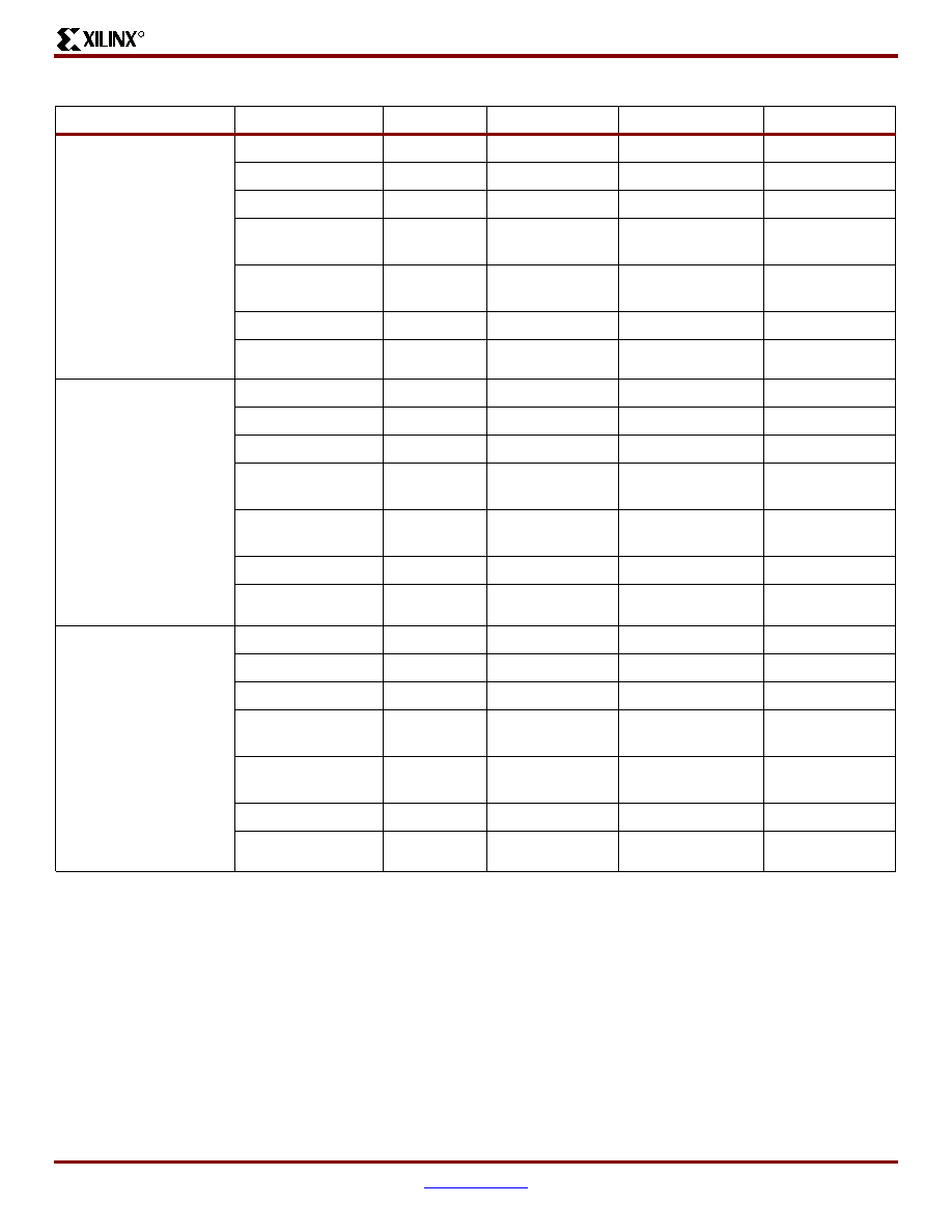
VirtexTM 2.5 V Field Programmable Gate Arrays
R
DS003-4 (v2.8) July 19, 2002
www.xilinx.com
Module 4 of 4
Production Product Specification
1-800-255-7778
13
V
REF
, Bank 1
(VREF pins are listed
incrementally. Connect
all pins listed for both
the required device and
all smaller devices
listed in the same
package.)
Within each bank, if
input reference voltage
is not required, all V
REF
pins are general I/O.
XCV50
B9, C11
N/A
N/A
N/A
XCV100/150
... + E11
A18, B13, E14
N/A
N/A
XCV200/300
... + A14
... + A19
N/A
N/A
XCV400
N/A
N/A
A14, C20, C21,
D15, G16
N/A
XCV600
N/A
N/A
... + B19
B6, B8, B18,
D11, D13, D17
XCV800
N/A
N/A
... + A17
... + B14
XCV1000
N/A
N/A
N/A
... + B5
V
REF
, Bank 2
(V
REF
pins are listed
incrementally. Connect
all pins listed for both
the required device and
all smaller devices
listed in the same
package.)
Within each bank, if
input reference voltage
is not required, all V
REF
pins are general I/O.
XCV50
F13, H13
N/A
N/A
N/A
XCV100/150
... + F14
F21, H18, K21
N/A
N/A
XCV200/300
... + E13
... + D22
N/A
N/A
XCV400
N/A
N/A
F24, H23, K20,
M23, M26
N/A
XCV600
N/A
N/A
... + G26
G1, H4, J1, L2,
V5, W3
XCV800
N/A
N/A
... + K25
... + N1
XCV1000
N/A
N/A
N/A
... + D2
V
REF
, Bank 3
(V
REF
pins are listed
incrementally. Connect
all pins listed for both
the required device and
all smaller devices
listed in the same
package.)
Within each bank, if
input reference voltage
is not required, all V
REF
pins are general I/O.
XCV50
K16, L14
N/A
N/A
N/A
XCV100/150
... + L13
N21, R19, U21
N/A
N/A
XCV200/300
... + M13
... + U20
N/A
N/A
XCV400
N/A
N/A
R23, R25, U21,
W22, W23
N/A
XCV600
N/A
N/A
... + W26
AC1, AJ2, AK3,
AL4, AR1, Y1
XCV800
N/A
N/A
... + U25
... + AF3
XCV1000
N/A
N/A
N/A
... + AP4
Table 4: Virtex Pinout Tables (Fine-Pitch BGA) (Continued)
Pin Name
Device
FG256
FG456
FG676
FG680
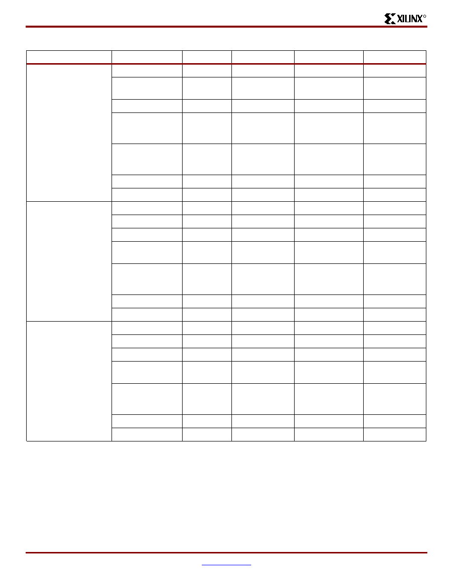
VirtexTM 2.5 V Field Programmable Gate Arrays
R
Module 4 of 4
www.xilinx.com
DS003-4 (v2.8) July 19, 2002
14
1-800-255-7778
Production Product Specification
V
REF
, Bank 4
(V
REF
pins are listed
incrementally. Connect
all pins listed for both
the required device and
all smaller devices
listed in the same
package.)
Within each bank, if
input reference voltage
is not required, all V
REF
pins are general I/O.
XCV50
P9, T12
N/A
N/A
N/A
XCV100/150
... + T11
AA13, AB16,
AB19
N/A
N/A
XCV200/300
... + R13
... + AB20
N/A
N/A
XCV400
N/A
N/A
AC15, AD18,
AD21, AD22,
AF15
N/A
XCV600
N/A
N/A
... + AF20
AT19, AU7,
AU17, AV8,
AV10, AW11
XCV800
N/A
N/A
... + AF17
... + AV14
XCV1000
N/A
N/A
N/A
... + AU6
V
REF
, Bank 5
(V
REF
pins are listed
incrementally. Connect
all pins listed for both
the required device and
all smaller devices
listed in the same
package.)
Within each bank, if
input reference voltage
is not required, all V
REF
pins are general I/O.
XCV50
T4, P8
N/A
N/A
N/A
XCV100/150
... + R5
W8, Y10, AA5
N/A
N/A
XCV200/300
... + T2
... + Y6
N/A
N/A
XCV400
N/A
N/A
AA10, AB8, AB12,
AC7, AF12
N/A
XCV600
N/A
N/A
... + AF8
AT27, AU29,
AU31, AV35,
AW21, AW23
XCV800
N/A
N/A
... + AE10
... + AT25
XCV1000
N/A
N/A
N/A
... + AV36
V
REF
, Bank 6
(V
REF
pins are listed
incrementally. Connect
all pins listed for both
the required device and
all smaller devices
listed in the same
package.)
Within each bank, if
input reference voltage
is not required, all V
REF
pins are general I/O.
XCV50
J3, N1
N/A
N/A
N/A
XCV100/150
... + M1
N2, R4, T3
N/A
N/A
XCV200/300
... + N2
... + Y1
N/A
N/A
XCV400
N/A
N/A
AB3, R1, R4, U6,
V5
N/A
XCV600
N/A
N/A
... + Y1
AB35, AD37,
AH39, AK39,
AM39, AN36
XCV800
N/A
N/A
... + U2
... + AE39
XCV1000
N/A
N/A
N/A
... + AT39
Table 4: Virtex Pinout Tables (Fine-Pitch BGA) (Continued)
Pin Name
Device
FG256
FG456
FG676
FG680

VirtexTM 2.5 V Field Programmable Gate Arrays
R
DS003-4 (v2.8) July 19, 2002
www.xilinx.com
Module 4 of 4
Production Product Specification
1-800-255-7778
15
V
REF
, Bank 7
(V
REF
pins are listed
incrementally. Connect
all pins listed for both
the required device and
all smaller devices
listed in the same
package.)
Within each bank, if
input reference voltage
is not required, all V
REF
pins are general I/O.
XCV50
C1, H3
N/A
N/A
N/A
XCV100/150
... + D1
E2, H4, K3
N/A
N/A
XCV200/300
... + B1
... + D2
N/A
N/A
XCV400
N/A
N/A
F4, G4, K6, M2,
M5
N/A
XCV600
N/A
N/A
... + H1
E38, G38, L36,
N36, U36, U38
XCV800
N/A
N/A
... + K1
... + N38
XCV1000
N/A
N/A
N/A
... + F36
GND
All
A1, A16, B2,
B15, F6, F7,
F10, F11,
G6, G7, G8,
G9, G10,
G11, H7,
H8, H9, H10,
J7, J8, J9,
J10, K6, K7,
K8, K9, K10,
K11, L6, L7,
L10, L11,
R2, R15, T1,
T16
A1, A22, B2,
B21, C3, C20,
J9, J10, J11,
J12, J13, J14,
K9, K10, K11,
K12, K13, K14,
L9, L10, L11,
L12, L13, L14,
M9, M10, M11,
M12, M13, M14,
N9, N10, N11,
N12, N13, N14,
P9, P10, P11,
P12, P13, P14,
Y3, Y20, AA2,
AA21, AB1,
AB22
A1, A26, B2, B9,
B14, B18, B25,
C3, C24, D4, D23,
E5, E22, J2, J25,
K10, K11, K12,
K13, K14, K15,
K16, K17, L10,
L11, L12, L13,
L14, L15, L16,
L17, M10, M11,
M12, M13, M14,
M15, M16, M17,
N2, N10, N11,
N12, N13, N14,
N15, N16, N17,
P10, P11, P12,
P13, P14, P15,
P16, P17, P25,
R10, R11, R12,
R13, R14, R15,
R16, R17, T10,
T11, T12, T13,
T14, T15, T16,
T17, U10, U11,
U12, U13, U14,
U15, U16, U17,
V2, V25, AB5,
AB22, AC4, AC23,
AD3, AD24, AE2,
AE9, AE13, AE18,
AE25, AF1, AF26
A1, A2, A3, A37,
A38, A39, AA5,
AA35, AH4,
AH5, AH35,
AH36, AR5,
AR12, AR19,
AR20, AR21,
AR28, AR35,
AT4, AT12, AT20,
AT28, AT36,
AU1, AU3, AU20,
AU37, AU39,
AV1, AV2, AV38,
AV39, AW1,
AW2, AW3,
AW37, AW38,
AW39, B1, B2,
B38, B39, C1,
C3, C20, C37,
C39, D4, D12,
D20, D28, D36,
E5, E12, E19,
E20, E21, E28,
E35, M4, M5,
M35, M36, W5,
W35, Y3, Y4, Y5,
Y35, Y36, Y37
Table 4: Virtex Pinout Tables (Fine-Pitch BGA) (Continued)
Pin Name
Device
FG256
FG456
FG676
FG680

VirtexTM 2.5 V Field Programmable Gate Arrays
R
Module 4 of 4
www.xilinx.com
DS003-4 (v2.8) July 19, 2002
16
1-800-255-7778
Production Product Specification
No Connect
(No-connect pins are
listed incrementally. All
pins listed for both the
required device and all
larger devices listed in
the same package are
no connects.)
XCV800
N/A
N/A
A2, A3, A15, A25,
B1, B6, B11, B16,
B21, B24, B26,
C1, C2, C25, C26,
F2, F6, F21, F25,
L2, L25, N25, P2,
T2, T25, AA2,
AA6, AA21, AA25,
AD1, AD2, AD25,
AE1, AE3, AE6,
AE11, AE14,
AE16, AE21,
AE24, AE26, AF2,
AF24, AF25
N/A
XCV600
N/A
N/A
same as above
N/A
XCV400
N/A
N/A
... + A9, A10, A13,
A16, A24, AC1,
AC25, AE12,
AE15, AF3, AF10,
AF11, AF13,
AF14, AF16,
AF18, AF23, B4,
B12, B13, B15,
B17, D1, D25,
H26, J1, K26, L1,
M1, M25, N1, N26,
P1, P26, R2, R26,
T1, T26, U26, V1
N/A
XCV300
N/A
D4, D19, W4,
W19
N/A
N/A
XCV200
N/A
... + A2, A6, A12,
B11, B16, C2,
D1, D18, E17,
E19, G2, G22,
L2, L19, M2,
M21, R3, R20,
U3, U18, Y22,
AA1, AA3, AA11,
AA16, AB7,
AB12, AB21,
N/A
N/A
XCV150
N/A
... + A13, A14,
C8, C9, E13,
F11, H21, J1, J4,
K2, K18, K19,
M17, N1, P1, P5,
P22, R22, W13,
W15, AA9,
AA10, AB8,
AB14
N/A
N/A
Table 4: Virtex Pinout Tables (Fine-Pitch BGA) (Continued)
Pin Name
Device
FG256
FG456
FG676
FG680
VirtexTM 2.5 V Field Programmable Gate Arrays
R
DS003-4 (v2.8) July 19, 2002
www.xilinx.com
Module 4 of 4
Production Product Specification
1-800-255-7778
17
Pinout Diagrams
The following diagrams, CS144 Pin Function Diagram
,
page 17
through FG680 Pin Function Diagram
, page 27
,
illustrate the locations of special-purpose pins on Virtex
FPGAs.
Table 5
lists the symbols used in these diagrams.
The diagrams also show I/O-bank boundaries.
CS144 Pin Function Diagram
Table 5: Pinout Diagram Symbols
Symbol
Pin Function
General I/O
Device-dependent general I/O, n/c on
smaller devices
V
V
CCINT
v
Device-dependent V
CCINT
, n/c on smaller
devices
O
V
CCO
R
V
REF
r
Device-dependent V
REF
, remains I/O on
smaller devices
G
Ground
ÿ, 1, 2, 3
Global Clocks
, ,
M0, M1, M2
, , ,
,
, , ,
D0/DIN, D1, D2, D3, D4, D5, D6, D7
B
DOUT/BUSY
D
DONE
P
PROGRAM
I
INIT
K
CCLK
W
WRITE
S
CS
T
Boundary-scan Test Access Port
+
Temperature diode, anode
≠
Temperature diode, cathode
n
No connect
Table 5: Pinout Diagram Symbols (Continued)
Symbol
Pin Function
Figure 1: CS144 Pin Function Diagram
1 2 3 4 5 6 7
9
10 11 12 13
8
1
ÿ
CS144
(Top view)
2
3
K
P
D
I
B
W
S
T
A
G
1 2 3 4 5 6 7
9
10 11 12 13
8
B
C
D
E
F
G
H
J
K
L
M
N
A
B
C
D
E
F
G
H
J
K
L
M
N
T
V
O
R
G
A
B
C
D
E
F
G
H
J
K
L
M
N
T
T
V
V
V
V
V
V
V
O
O
O
O
O
O
O
O
O
O
O
R
r
R
R
r
R
R
r
R
R
r
R
R
R
R
r
R
R
r
R
R
r
G
G
G
G
G
G
G
G
G
G
G
G
G
G
r
Bank 0
Bank 1
Bank 5
Bank 3
Bank 4
Bank 6
Bank 2
Bank 7

VirtexTM 2.5 V Field Programmable Gate Arrays
R
Module 4 of 4
www.xilinx.com
DS003-4 (v2.8) July 19, 2002
18
1-800-255-7778
Production Product Specification
TQ144 Pin Function Diagram
Figure 2: TQ144 Pin Function Diagram
1
2
3
4
5
6
7
9
10
11
12
13
14
15
16
17
19
20
21
22
23
24
25
26
27
29
30
31
32
33
34
35
36
8
18
28
37
39 40 41 42 43 44 45 46 47
49 50 51 52 53 54 55 56 57
59 60 61 62 63 64 65 66
38
48
58
67
69 70 71 72
68
73
74
75
76
77
79
80
81
82
83
84
85
86
87
89
90
91
92
93
94
95
96
78
88
97
99
100
98
101
102
103
104
105
106
107
108
109
110
111
112
113
114
115
116
117
119
120
121
122
123
124
125
126
127
129
130
131
132
133
134
135
136
118
128
137
139
140
141
142
143
144
138
1
ÿ
TQ144
(Top view)
2
3
K
P
D
I
B
W
S
T
T
T
T
V
V
V
V
V
V
V
V
O
O
O
O
O
O
O
O
R
r
R
R
R
R
R
R
R
R
R
R
R
R
R
R
R
G
G
G
G
G
G
G
G
G
G
G
G
G
G
G
G
r
r
r
r
r
r
r
Bank 0
Bank 7
Bank 6
Bank 5
Bank 1
Bank 4
Bank 2
Bank 3

VirtexTM 2.5 V Field Programmable Gate Arrays
R
DS003-4 (v2.8) July 19, 2002
www.xilinx.com
Module 4 of 4
Production Product Specification
1-800-255-7778
19
PQ240/HQ240 Pin Function Diagram
Figure 3: PQ240/HQ240 Pin Function Diagram
T
O
T
r
G
R
r
r
G
O
V
G
R
r
V
3
O
G
2
r
R
G
V
O
G
r
r
R
G
r
W
S
T
G
T
r
G
R
r
r
G
O
V
G
R
r
G
O
V
r
R
G
V
O
G
r
r
R
G
r
G
O
K
B
r
G
R
r
r
G
O
V
G
R
r
G
O
V
r
R
G
V
O
G
r
r
R
G
r
I
P
O
r
G
R
r
r
G
O
V
G
R
r
V
1
O
G
ÿ
r
R
G
V
O
G
r
r
R
G
r
G
D
O
1
G
3
5
7
9
11
13
15
17
19
21
23
25
27
29
31
33
35
37
39
41
43
45
47
49
51
53
55
57
59
61
63
65
67
69
71
73
75
77
79
81
83
85
87
89
91
93
95
97
99
101
103
105
107
109
111
113
115
117
119
121
123
125
127
129
131
133
135
137
139
141
143
145
147
149
151
153
155
157
159
161
163
165
167
169
171
173
175
177
179
181
18
3
185
187
18
9
191
19
3
195
197
19
9
201
20
3
205
207
20
9
211
21
3
215
217
21
9
221
22
3
225
227
22
9
231
23
3
235
237
23
9
PQ240/HQ240
(Top view)
Pins are shown staggered
for readability
Bank 0
Bank 7
Bank 6
Bank 5
Bank 4
Bank 3
Bank 2
Bank 1
r
r
r
r
r
r
r
r
VirtexTM 2.5 V Field Programmable Gate Arrays
R
Module 4 of 4
www.xilinx.com
DS003-4 (v2.8) July 19, 2002
20
1-800-255-7778
Production Product Specification
BG256 Pin Function Diagram
Figure 4: BG256 Pin Function Diagram
1
2
3
4
5
6
7
8
9
10
11
12
13
14
15
16
17
18
19
20
B
C
D
E
F
G
H
J
K
L
M
N
P
R
T
U
V
W
Y
A
ÿ
r
B
C
D
E
F
G
H
J
K
L
M
N
P
R
T
U
V
W
Y
A
1
2
3
4
5
6
7
8
9
10
11
12
13
14
15
16
17
18
19
20
Bank 0
Bank 1
Bank 5
Bank 3
Bank 4
Bank 6
Bank 2
Bank 7
BG256
(Top View)
r
r
r
r
r
r
r
r
T
R
2
R
W T
R
V
R
S K
G
3
T G
R
T G G V O O G G G G O O V G G B
G
G
V
V
R O
O
R
O
O
G
G G G G
G G G G
G G G G
G G G G
G R
G
G
V G
G V
R
G
G R
O
O
O
O
R V
V
G
G
G G V O O G G G G O O V G G I
G +
R V
R
G
R
≠
D
R
1
R
P
r
r
r
r
r
r
r
DS003_18_100300

VirtexTM 2.5 V Field Programmable Gate Arrays
R
DS003-4 (v2.8) July 19, 2002
www.xilinx.com
Module 4 of 4
Production Product Specification
1-800-255-7778
21
BG352 Pin Function Diagram
Figure 5: BG352 Pin Function Diagram
G
1
2
3
4
5
6
7
8
9
10
11
12
13
14
15
16
17
18
19
20
21
22
23
24
25
26
B
C
D
E
F
G
H
J
K
L
M
N
P
R
T
U
V
W
Y
AA
AB
AC
AD
AE
AF
G
G
V
G
O
R
G
O
G
G
G
G
A
G
O
V
2
R
T
O
G
T
R
R
V
R
R
S
K
R
T
r
O
3
O
V
V
O
r
T
r
O
R
R
O
R
V
O
P
r
r
≠
R
D
I
G
O
+
r
V
V
ÿ
R
R
r
O
G
G
G
G
G
O
V
1
G
V
O
G
G
G
G
G
r
R
O
G
V
O
R
V
O
G
V
R
V
O
V
G
O
R
R
G
B
R
G
O
R
G
V
O
V
R
G
O
V
R
V
O
R
V
G
O
R
G
B
C
D
E
F
G
H
J
K
L
M
N
P
R
T
U
V
W
Y
AA
AB
AC
AD
AE
AF
A
1
2
3
4
5
6
7
8
9
10
11
12
13
14
15
16
17
18
19
20
21
22
23
24
25
26
Bank 1
Bank 0
Bank 4
Bank 6
Bank 5
Bank 3
Bank 7
Bank 2
BG352
(Top View)
W
DS003_19_100600
VirtexTM 2.5 V Field Programmable Gate Arrays
R
Module 4 of 4
www.xilinx.com
DS003-4 (v2.8) July 19, 2002
22
1-800-255-7778
Production Product Specification
BG432 Pin Function Diagram
Figure 6: BG432 Pin Function Diagram
1
2
3
4
5
6
7
8
9
10
11
12
13
14
15
16
17
18
19
20
21
22
23
24
25
26
B
C
D
E
F
G
H
J
K
L
M
N
P
R
T
U
V
W
Y
AA
AB
AC
AD
AE
AF
A
r
B
C
D
E
F
G
H
J
K
L
M
N
P
R
T
U
V
W
Y
AA
AB
AC
AD
AE
AF
A
1
2
3
4
5
6
7
8
9
10
11
12
13
14
15
16
17
18
19
20
21
22
23
24
25
26
Bank 1
Bank 0
Bank 4
Bank 6
Bank 5
Bank 3
Bank 7
Bank 2
BG432
(Top View)
27
28
29
30
31
27
28
29
30
31
AG
AH
AJ
AK
AL
AG
AH
AJ
AK
AL
R
R
O
G
V
G
R
V
1
V
G I O
O
O
R
V R
R
+
D
G G
G
O
G G
G
R G
ÿ
G
O G
P
G R
G
G R
≠
O
R
V
G
O
G
V
R
G O
G
R
O
V
R
O
O
G
R
O G G
G
G V O
R G
2 V G
O
G
G
G
G
O
G G T W
R
R
V
G
G
G
O T
R
R
V
V
R
O
G
B K S
O
G 3
O R
R
T T
R
R
R
G
R
G
G R
R G
V
O
O
O
O
R V
V R
G
G
V
G
G V
G R
R
G
V
V
V
V
V
r
r
r
r
r
r
V
r
r
r
V
V
r
r
r
V
V
r
r
r
r
r
r
r
r
r
r
r
V
G
DS003_21_100300
VirtexTM 2.5 V Field Programmable Gate Arrays
R
DS003-4 (v2.8) July 19, 2002
www.xilinx.com
Module 4 of 4
Production Product Specification
1-800-255-7778
23
BG560 Pin Function Diagram
Figure 7: BG560 Pin Function Diagram
1
2
3
4
5
6
7
8
9
10
11
12
13
14
15
16
17
18
19
20
21
22
23
24
25
26
K
T
≠
I
+
ÿ
O
1
B
1
2
3
4
5
6
7
8
9
10
11
12
13
14
15
16
17
18
19
20
21
22
23
24
25
26
Bank 1
Bank 0
Bank 4
Bank 6
Bank 5
Bank 3
Bank 7
Bank 2
BG560
(Top View)
W
27
28
29
30
31
32
33
27
28
29
30
31
32
33
B
C
D
E
F
G
H
J
K
L
M
N
P
R
T
U
V
W
Y
AA
AB
AC
AD
AE
AF
A
AG
AH
AJ
AK
AL
AM
AN
B
C
D
E
F
G
H
J
K
L
M
N
P
R
T
U
V
W
Y
AA
AB
AC
AD
AE
AF
A
AG
AH
AJ
AK
AL
AM
AN
R
O
R
O
G
O
G
G
R
G
O
G
P
R
V
V
G
R
R V G
G
R
R
G
R
G
n
O
R
O
V
R
R
V
n
R
O
G
O
O
G
G
G
O
G
O
O
V
V G
O V R
O G
G
O
G
G
G
O
V
G
V
G
V
O
R
G
G
G
R
G S
R G
O
G
G
O 3 G
G
R
V O
G
O
G O
G G
G O
G
G
V
V
O
G
V O
G
G V
G O T
G O
V
n O
O
T
R
R
R 2
R
R
R
O
G
O T r
V
V
R
R
R
V
G
G
R
R
G
O
R
V
V
G
G
R V O
G
R
O
G
V
O V
G
R
R
G
O
R
G
G
R
O
V
V
O
R
R
G
G
R
O
G V
V R G
D
n
V
V
V
V
V
V
V
r
r
r
r
r
r
r
r
r
r
r
r
r
r
r
r
r
r
r
r
r
r
r
DS003_22_100300

VirtexTM 2.5 V Field Programmable Gate Arrays
R
Module 4 of 4
www.xilinx.com
DS003-4 (v2.8) July 19, 2002
24
1-800-255-7778
Production Product Specification
FG256 Pin Function Diagram
Figure 8: FG256 Pin Function Diagram
3
1
ÿ
FG256
(Top view)
2
3
K
P
D
I
B
W
S
T
V
O
≠
G
1 2
4 5 6 7
9
10 11 12 13
8
A
B
C
D
E
F
G
H
J
K
L
M
N
P
R
T
16
14 15
1 2 3 4 5 6 7
9
10 11 12 13
8
16
14 15
A
B
C
D
E
F
G
H
J
K
L
M
N
P
R
T
T
T
T
+
V
V
V
V
V
V
V
V
V
V
V
O
O O
O O
O O
O O
O O
O O
O O
R
R
r
R
R
R
R
R
R
R
R
R
R
R
R
R
R
G
G
G
G
G
G
G
G G
G
G
G G
G
G
G G
G
G
G G
G
G
G G
G
G
G G
G
G
G G
G G
r
r
r
r
r
r
r
r
r
r
r
r
r
r
r
Bank 0
Bank 1
Bank 5
Bank 3
Bank 4
Bank 6
Bank 2
Bank 7
VirtexTM 2.5 V Field Programmable Gate Arrays
R
DS003-4 (v2.8) July 19, 2002
www.xilinx.com
Module 4 of 4
Production Product Specification
1-800-255-7778
25
FG456 Pin Function Diagram
Notes:
Packages FG456 and FG676 are layout compatible.
Figure 9: FG456 Pin Function Diagram
2
1
3 4 5 6 7
9
10 11 12 13
8
16
14 15
17 18 19 20 21 22
1
ÿ
FG456
(Top view)
2
3
K
P
D
I
B
W
S
T
V
O
R
n
≠
G
A
B
C
D
E
F
G
H
J
K
L
M
N
P
R
T
U
V
W
Y
AA
AB
A
B
C
D
E
F
G
H
J
K
L
M
N
P
R
T
U
V
W
Y
AA
AB
1 2 3 4 5 6 7
9
10 11 12 13
8
16
14 15
17 18 19 20 21 22
T
T
T
+
V
V
V
V
V
V
V V V
V
V
V
V
V
V
V
V V
V
V
V
V
V
V
V
V
V
O O O
O O O O
O O O O
O O O O
O O O O
O O O O
O
O
O
O O
O
O
O
O
O
O
O
O
O
O
O
O
O
O
O
O
O
O
O
r
R
R
R
R
R
R
R
R
R
R
R
R
R
R
R
R
R
R
R
R
R
R
R
G
G
G
G
G
G
G
G
G
G
G
G G G G G G
G G G G G G
G G G G G G
G G G G G G
G G G G G G
G G G G G G
n
n
n
r
r
r
r
r
r
r
Bank 0
Bank 1
Bank 5
Bank 3
Bank 4
Bank 6
Bank 2
Bank 7

VirtexTM 2.5 V Field Programmable Gate Arrays
R
Module 4 of 4
www.xilinx.com
DS003-4 (v2.8) July 19, 2002
26
1-800-255-7778
Production Product Specification
FG676 Pin Function Diagram
Notes:
Packages FG456 and FG676 are layout compatible.
Figure 10: FG676 Pin Function Diagram
1
2
3
4
5
6
7
8
9
10
11
12
13
14
15
16
17
18
19
20
21
22
23
24
25
26
A
G n n
R R n r n G
A
B
n G
n r G r n G n G r n n G n
B
C
n n G
R 2 R R W T G n n
C
D
G R R T G K
D
E
G T R 3 S G B
E
Bank 7
F
n R T n n
R n
F
Bank 2
G
R V R R V r
G
H
r
V O O O O O O O O V R
H
J
G O V V V O O O O V V V O G
J
K
r
R O V G G G G G G G G V O R
r
K
L
n O V G G G G G G G G V O n
L
M
R R O O G G G G G G G G O O
R
R
M
N
G O G G G G G G G G O n
N
P
n O G G G G G G G G O G
P
R
R
R O O G G G G G G G G O O R
R
R
T
n O V G G G G G G G G V O n
T
U
r R O V G G G G G G G G V O R
r
U
V
G R O V V V O O O O V V V O
G
V
Bank 6
W
V O O O O
O O O O V R R r
W
Bank 3
Y
r
V
+
V I
Y
AA
n n R 0 n P n
AA
AB
R G
R
R 1 D G
AB
AC
G R R G
AC
AD
n n G
R R R G
n
AD
AE
n G n
n G r n G n n G n n G n
AE
AF
G n
r R R r r n n G
AF
1
2
3
4
5
6
7
8
9
10
11
12
13
14
15
16
17
18
19
20
21
22
23
24
25
26
Bank 0
Bank 1
Bank 5
Bank 4
fg676a
-
FG676
(Top view)
VirtexTM 2.5 V Field Programmable Gate Arrays
R
DS003-4 (v2.8) July 19, 2002
www.xilinx.com
Module 4 of 4
Production Product Specification
1-800-255-7778
27
FG680 Pin Function Diagram
Figure 11: FG680 Pin Function Diagram
Bank 1
Bank 0
1
2
3
4
5
6
7
8
9
10
11
12
13
14
15
16
17
18
19
20
21
22
23
24
25
26
27
28
29
30
31
32
33
34
35
36
37
38
39
A
G G G
3 r R G G G
A
B
G G T W r
R
R r R R R G G
B
C
G
G T
G R R T G G
C
D
r G S R G R R G 2 G R r G
D
E
B K G O O V V O O G O O V V G G G V V O O G O O V V O O G T R
E
Bank 2
F
O
O
r
F
Bank 7
G
R
O
O
R
G
H
R V
V
H
J
R
V
V
J
K
O
O
K
L
R O
O R
L
M
G G
G G
M
N
r
O
O R
r
N
P
O
O
P
R
V
V
R
T
V
V
T
U
R R
U
V
R
V
W
R G
G
W
Y
R
G G G
G G G
Y
AA
G
G
AA
AB
R
AB
AC
R
AC
AD
V
V
R
AD
AE
V
V
r
AE
AF
r O
O
AF
AG
O
O
AG
AH
G G
G G
R
AH
AJ
R O
O
AJ
AK
R O
O
R
AK
AL
R V
V
AL
AM
V
V
R
AM
AN
O
O R
AN
Bank 3
AP
r O
O
AP
Bank 6
AR
R
G O O V V O O G O O V V
G G G V V O O G O O V V O O G
AR
AT
G P G R G r R G
G
r
AT
AU
G
I
G
D r R R G 1 R R
+
G
G
AU
AV
G G
R R r R r
G G
AV
AW
G G G
R 0 R R G G G
AW
1
2
3
4
5
6
7
8
9
10
11
12
13
14
15
16
17
18
19
20
21
22
23
24
25
26
27
28
29
30
31
32
33
34
35
36
37
38
39
Bank 4
Bank 5
fg680_12a
-
FG680
(
Top View)
Bank 2
Note: AA3, AA4, and AB2 are in Bank 2
Bank 7
Note: AA37 is in Bank 7
VirtexTM 2.5 V Field Programmable Gate Arrays
R
Module 4 of 4
www.xilinx.com
DS003-4 (v2.8) July 19, 2002
28
1-800-255-7778
Production Product Specification
Revision History
Virtex Data Sheet
The Virtex Data Sheet contains the following modules:
∑
DS003-1, Virtex 2.5V FPGAs:
Introduction and Ordering Information (Module 1)
∑
DS003-2, Virtex 2.5V FPGAs:
Functional Description (Module 2)
∑
DS003-3, Virtex 2.5V FPGAs:
DC and Switching Characteristics (Module 3)
∑
DS003-4, Virtex 2.5V FPGAs:
Pinout Tables (Module 4)
Date
Version
Revision
11/98
1.0
Initial Xilinx release.
01/99
1.2
Updated package drawings and specs.
02/99
1.3
Update of package drawings, updated specifications.
05/99
1.4
Addition of package drawings and specifications.
05/99
1.5
Replaced FG 676 & FG680 package drawings.
07/99
1.6
Changed Boundary Scan Information and changed Figure 11, Boundary Scan Bit
Sequence. Updated IOB Input & Output delays. Added Capacitance info for different I/O
Standards. Added 5 V tolerant information. Added DLL Parameters and waveforms and
new Pin-to-pin Input and Output Parameter tables for Global Clock Input to Output and
Setup and Hold. Changed Configuration Information including Figures 12, 14, 17 & 19.
Added device-dependent listings for quiescent currents ICCINTQ and ICCOQ. Updated
IOB Input and Output Delays based on default standard of LVTTL, 12 mA, Fast Slew Rate.
Added IOB Input Switching Characteristics Standard Adjustments.
09/99
1.7
Speed grade update to preliminary status, Power-on specification and Clock-to-Out
Minimums additions, "0" hold time listing explanation, quiescent current listing update, and
Figure 6 ADDRA input label correction. Added T
IJITCC
parameter, changed T
OJIT
to T
OPHASE
.
01/00
1.8
Update to speed.txt file 1.96. Corrections for CRs 111036,111137, 112697, 115479,
117153, 117154, and 117612. Modified notes for Recommended Operating Conditions
(voltage and temperature). Changed Bank information for V
CCO
in CS144 package on p.43.
01/00
1.9
Updated DLL Jitter Parameter table and waveforms, added Delay Measurement
Methodology table for different I/O standards, changed buffered Hex line info and
Input/Output Timing measurement notes.
03/00
2.0
New TBCKO values; corrected FG680 package connection drawing; new note about status
of CCLK pin after configuration.
05/00
2.1
Modified "Pins not listed ..." statement. Speed grade update to Final status.
05/00
2.2
Modified Table 18.
09/00
2.3
∑
Added XCV400 values to table under Minimum Clock-to-Out for Virtex Devices.
∑
Corrected Units column in table under IOB Input Switching Characteristics.
∑
Added values to table under CLB SelectRAM Switching Characteristics.
10/00
2.4
∑
Corrected pinout info for devices in the BG256, BG432, and BG560 pkgs in Table 18.
∑
Corrected BG256 Pin Function Diagram.
04/02/01
2.5
∑
Revised minimums for Global Clock Set-Up and Hold for LVTTL Standard, with DLL.
∑
Converted file to modularized format. See section
Virtex Data Sheet
, below.
04/19/01
2.6
∑
Corrected pinout information for FG676 device in
Table 4
. (Added AB22 pin.)
07/19/01
2.7
∑
Clarified V
CCINT
pinout information and added AE19 pin for BG352 devices in
Table 3
.
∑
Changed pinouts listed for BG352 XCV400 devices in banks 0 thru 7.
07/19/02
2.8
∑
Changed pinouts listed for GND in TQ144 devices (see
Table 2
).