
September 16, 1999
1
7810 South Hardy Drive, Suite 104
Tempe, Arizona 85284 USA
Phone:
+1 888-845-5585 (USA)
+1 480-753-5585
Fax:
+1 480-753-5899
E-mail:
info@memecdesign.com
URL:
www.memecdesign.com
Features
∑
I
2
C-compatible two-wire serial interface core;
I
2
C is a
trademark of Philips, Inc
.
∑
Multi-master operation with arbitration and clock
synchronization
∑
Slave transmit and receive operation
∑
Support for reads, writes, burst reads, burst writes, and
repeated start
∑
User-defined timing and clock frequency
∑
Fast mode and standard mode operation
Applications
∑
Embedded microprocessor boards and any circuit
needing I
2
C peripherals.
AllianceCORE
TM
Facts
Core Specifics
See Table 1
Provided with Core
Documentation
Datasheet,
Implementation instructions
Design File Formats
VHDL Source RTL
Constraints File
.ucf
Verification
VHDL Testbench
Instantiation
Templates
VHDL, Verilog
Reference designs &
Application notes
None
Additional Items
Warranty by MDS
Simulation Tool Used
Model Technology
Support
Support provided by Memec Design Services.
September 16, 1999
Product Specification
XF-TWSI-MS Two-Wire Serial
Interface Master-Slave
Table 1: Core Implementation Data
Supported
Family
Device
Tested
CLBs
2
Clock
IOBs
IOBs
1
Performance
(MHz)
Xilinx
Tools
Special
Features
Core
Core+
Ext logic
Core
Core+
Ext logic
4000XL
4005XL-1
156
156
2
31
29
31
M1.5i
TBUFs
Spartan
S10-4
164
164
2
31
29
30
M1.5i
TBUFs
Virtex
V50-4
185
2
185
2
2
31
29
59
M1.5i
TBUFs
Notes:
1. Assuming all core I/O are routed off-chip.
2. Utilization numbers for Virtex are in CLB slices.
XF-TWSI-MS Two-Wire Serial Interface Master-Slave
2
September 16, 1999
General Description
XF-TWSI-MS is an industry standard two-wire serial inter-
face supporting multiple masters. This core will operate as
a master or a slave. This core does not support General
Call Addressing, 10-bit slave addressing, or START byte
data transfers.
MDS cores are designed with the philosophy that no global
elements should be embedded within the core itself. Global
elements include any of the following components: STAR-
TUP, STARTBUF, BSCAN, READBACK, Global Buffers,
Fast Output Primitives, IOB Elements, Clock Delay Compo-
nents, and any of the Oscillator Macros. MDS cores only
contain resources present in the CLB array. This is done to
allow flexibility in using the cores with other logic. For
instance, if a global clock buffer is embedded within the
core, but some external logic also requires that same clock,
then an additional global buffer would have to be used.
In any instance, where one of our cores generates a clock,
that signal is brought out of the core, run through a global
buffer, and then brought back into the core. This philosophy
allows external logic to use that clock without using another
global buffer.
A result of this philosophy is that the cores are not self-con-
tained. External logic must be connected to the core inor-
der to complete it. MDS cores include tested sample
designs that add the external logic required to complete the
functionality. This datasheet describes both the core and
the supplied external logic.
The Absolute Maximum Ratings, Operating Conditions, DC
Electrical Specifications, and Capacitance are device
dependent and can be found in the Xilinx datasheet for the
target device.
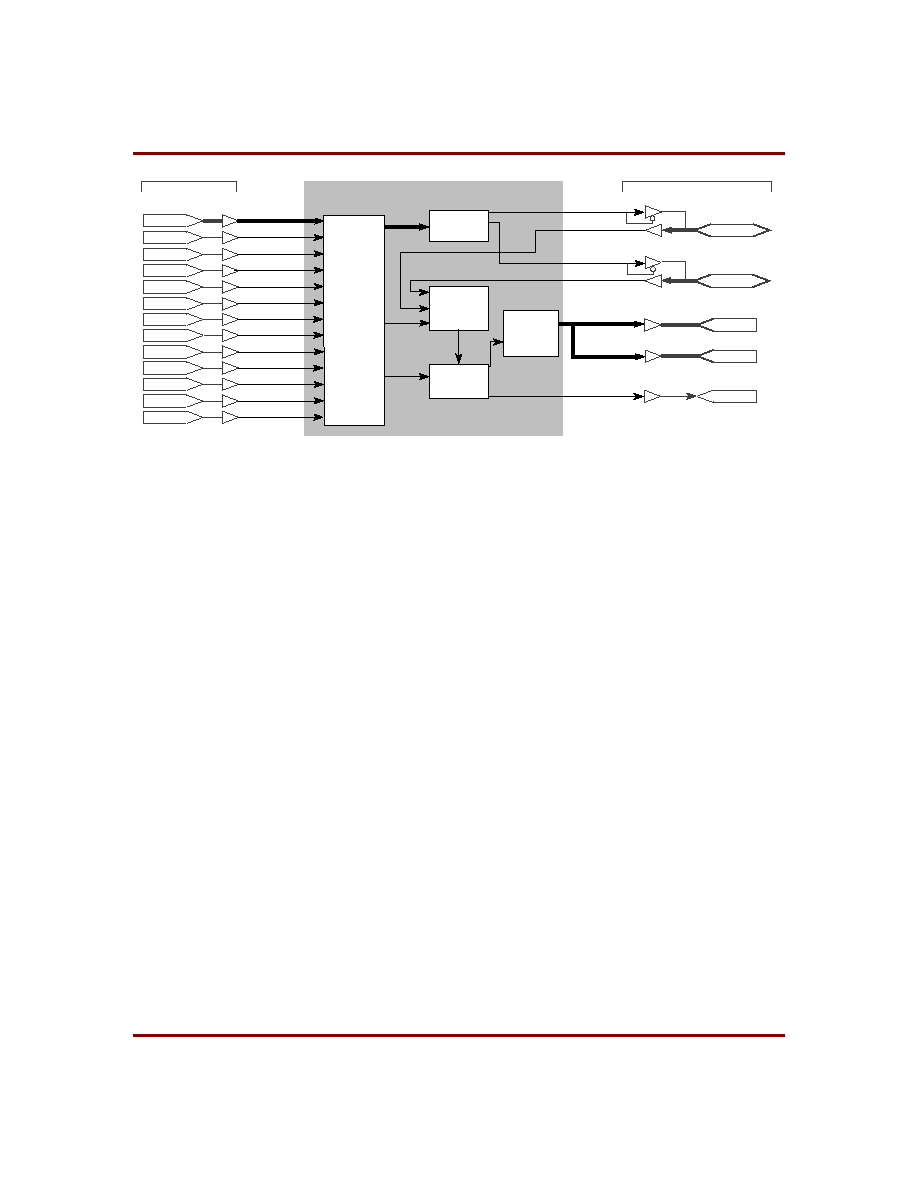
Functional Description
The XF-TWSI-MS is partitioned into modules as shown in
Figure 1 and described below.
Microprocessor Interface Control
Logic
There are four registers used to interface to the host: the
Data Register, the Address Register, the Own_Address
Register, and the Command Register. The Own_Address
Register is used for slave operations to set the unique
address of the device on the IIC bus. The strobes
WR_DATA, WR_ADDR, WR_OWN_ADDR, and
CMD_STAT are directly connected to the clock enable pins
of these register flip-flops for ease of interface.
Shiftlgc
The basic cycle on the XF-TWSI-MS serial interface con-
sists of an address cycle followed by a data cycle. The
address consists of seven bits and the read/write bit (the
LSB). The MSB is always transmitted first on the SDA line.
The data cycle can either be a read or a write. For a write
operation the macro shifts the data from the Data Register
onto the SDA line. For a read operation the macro captures
the data into the Shift Register. The data cycle can end in
three different ways:
1. A stop can be generated which terminates the current
cycle.
2. Another data cycle can take place (a burst).
Figure 1: XF-TWSI Block Diagram
X8902
RESET
MPU_DIN[7:0]
WR_L
WR_DATA
WR_ADDR
CMD_STAT
Micro-
Processor
Interface
Control
Logic
Synchrs
SCL_IN
RD_L
SCL_OUT
SDA_OUT
MPU_DOUT[3:0]
MPU_DOUT[7:0]
INTERRUPT
SDA_IN
I Pad
IBUF
IBUF
I Pad
IBUF
I Pad
IBUF
I Pad
IBUF
I Pad
IBUF
I Pad
IBUF
IBUF
OBUFT
I/O Pad
OBUFT
OBUF
I/O Pad
O Pad
OBUF
O Pad
OBUF
O Pad
(HOST DATA)
(STATUS REGISTER)
XFTWSI CORE
External Logic
External Logic
Shift
Register
AT TOP LEVEL
State
Machine
Shiftlgc
WR_FREE_CNT
WR_HI_CNT
WR_LO_CNT
TWSI_DATA
CLK
I Pad
IBUF
I Pad
IBUF
I Pad
IBUF
I Pad
IBUF
I Pad
BUFG
>
I Pad
WR_OWN_ADDR
IBUF
I Pad

September 16, 1999
3
Memec Design Services
3. A repeated start can be generated by the inter-face.
There is always one interrupt generated for each data cycle
independent of the type of cycle. For example, for a burst
read cycle an interrupt will be generated for each byte read.
For a burst write cycle an interrupt will be generated when
each byte transfer is completed.
A repeated start is used to turn the bus around; when a
read cycle must be followed directly by a write cycle without
a stop in-between. Since the READ bit is a part of the
address, if a read followed by write is desired without a stop
command, a second address must be issued following the
data cycle. The sequence of events in a repeated start
cycle is: start, address cycle, data cycle, repeated start,
address cycle, data cycle, stop. Each of the data cycles can
be repeated if bursting is desired, and the stop cycle could
actually be another repeated start, if desired.
Synchrs
The SDA and SCL inputs are passed through this module
that performs a dual-rank synchronization and glitch filter-
ing when enabled by the FILTER_EN signal. The synchro-
nized versions of the SDA and SCL signals are used in all
macro modules.
The XF-TWSI-MS macro treats both the SDA and SCL
lines as data lines. The SDA line is actually sampled some
number of clocks after the rising edge of SCL is detected.
This allows for greater noise immunity and more robust
operation.
State Machine
The control for the serial interface comes from the state
machine. This state machine controls the loading and
enabling of all shift registers and counters, and is responsi-
ble for implementing the basic interface protocol.
Shift Register
There is a single parallel-in, parallel-out, serial-in, serial-out
shift register called NUPSHIFT_MS, which performs the
shifting of data for address cycles, write cycles, and read
cycles. The parallel output drives the macro interface pins
MPU_DOUT which are used to return read data to the host.
Core Modifications
With minor exception, the XF-TWSI-MS meets or exceeds
the industry standard. However, in most cases the
Timespecs can be tightened significantly. Proper operation
with 100ns bus cycles has been verified. In all cases, a
post-route timing analysis should be performed to verify
performance. Implementation beyond specified perfor-
mance and other customizing is available through Memec
Design Services at additional cost.
External Crystal Support
This core does not support connection of a crystal directly
to the device; a clock input is required.
Pinout
Due to the open collector nature of the Serial Data
(SDA_IN and SDA_OUT) and Serial Clock (SCL_IN and
SCL_OUT) pins, the XF-TWSI-MS must be implemented
internally with the user's design using an OBUFT and IBUF
combination. Signal names are provided in the block dia-
gram shown in Figure 1 and Table 2.
Verification Methods
Complete functional and timing simulation has been per-
formed on the XF-TWSI-MS using Model Technology
VSIM. (Simulation command files and test bench used for
verification are provided with the core.)
Recommended Design Experience
Users should be familiar with VHDL, Xilinx design flows and
have experience with microprocessor systems and periph-
erals. For the source code version, users should also be
familiar with Synplicity's synthesis and Model Technology's
simulation tools.
Ordering Information
The XF-TWSI Two Wire Serial Interface Core is provided
under license from Memec Design Services for use in Xilinx
programmable logic devices and Xilinx HardWire gate
arrays. Please contact Memec for pricing and more infor-
mation.
Memec Design Services warrants that the design delivered
by Memec Design Services will conform to the design
specification. This warranty expires 3 months from the date
of delivery of the design database. Contact Memec De-sign
Services for the Design License Agreement with complete
Terms and Conditions of Sale.
Information furnished by Memec Design Services is
believed to be accurate and reliable. Memec Design Ser-
vices reserves the right to change specifications detailed in
this data sheet at any time without notice, in order to
improve reliability, function or design, and assumes no
responsibility for any errors within this document. Memec
Design Services does not make any commitment to update
this information.
Memec Design Services assumes no obligation to correct
any errors contained herein or to advise any user of this
text of any correction, if such be made, nor does the Com-
pany assume responsibility for the functioning of unde-
scribed features or parameters. Memec Design Services
will not assume any liability for the accuracy or correctness
of any support or assistance provided to a user.

XF-TWSI-MS Two-Wire Serial Interface Master-Slave
4
September 16, 1999
Memec Design Services does not represent that products
described herein are free from patent infringement or from
any other third-party right. No license is granted by implica-
tion or otherwise under any patent or patent rights of
Memec Design Services.

September 16, 1999
5
Memec Design Services
Table 2: Core Signal Pinout
Memec Design Services products are not intended for use
in life support appliances, devices, or systems. Use of a
Memec Design Services product in such application with-
out the written consent of the appropriate Memec Design
Services officer is prohibited.
All trademarks, registered trademarks, or servicemarks are
property of their respective owners.
Related Information
The I2C-Bus And How To Use It
Contact:
Philips Semiconductors
URL: www-eu.semiconductors.philips.com/i2c/
Signal
Signal
Direction
Description
MPU_DIN[7:0]
Input
Microprocessor Data In
lines; used to program Da-
ta, Address, and Command
Registers.
RESET
Input
Reset; active high.
RD_L
Input
Allows reads on
MPU_DOUT when active
"0" with proper read buffer/
register is selected.
WR_L
Input
Rising edge of this signal
registers data in internal
registers when proper ad-
dress is selected.
WR_DATA
Input
When active "1" with WR_L
strobes 8-bits from
MPU_DIN into Data Regis-
ter for serial bus write cycle.
WR_ADDR
Input
When active "1" with WR_L
strobes least significant 7-
bits of MPU_DIN into Ad-
dress Register for all Serial
Bus Operations.
WR_OWN_ADDR
Input
When active "1" with WR_L
strobes 8-bits from the
MPU_DIN into
OWN_ADDR register to set
address of device on I2C
bus.
CMD_STAT
Input
When active "1" with WR_L
strobes least significant 5-
bits from MPU_DIN into
Command Register, ini-
tiates serial bus cycle and
clears the Interrupt line.
When active "1" with RD_L
reads
status register.
WR_FREE_CNT
Input
When active "1" with WR_L
strobes 8-bits from
MPU_DIN into
BUSFREE_COUNT regis-
ter, used to set the bus free
period.
WR_HI_CNT
Input
When active "1" with WR_L
strobes 8-bits from
MPU_DIN into HI_COUNT
register, used to set number
of CLK clock periods for low
period of SCL and setup
time for repeated start oper-
ation.
Signal
Signal
Direction
Description
WR_LO_CNT
Input
When active "1" with WR_L
strobes 8-bits from the
MPU_DIN into LO_COUNT
register used to set number
of CLK clock periods for
high count of SCL, hold
time for start command, and
setup time for stop com-
mand.
TWSI_DATA
Input
Allows reads on
MPU_DOUT when active
"1" with RD_L.
CLK
Input
Primary clock.
SCL_OUT
Output
Serial clock with open col-
lector output.
SCL_IN
Input
Serial clock with open col-
lector input.
SDA_OUT
Output
Serial data with open col-
lector output.
SDA_IN
Input
Serial data with open col-
lector input.
MPU_DOUT[7:0]
Output
Returns read data after acti-
vation of Interrupt pin and
error free status; lower
three bits are also Status
Register.
INTERRUPT
Output
Interrupt line set upon com-
pletion or abort of serial cy-
cle; active high.

XF-TWSI-MS Two-Wire Serial Interface Master-Slave
6
September 16, 1999
Xilinx Programmable Logic
For information on Xilinx programmable logic or develop-
ment system software, contact your local Xilinx sales office,
or:
Xilinx, Inc.
2100 Logic Drive
San Jose, CA 95124
Phone:
+1 408-559-7778
Fax:
+1 408-559-7114
URL:
www.xilinx.com
For general Xilinx literature, contact:
Phone:
+1 800-231-3386 (inside the US)
+1 408-879-5017 (outside the US)
E-mail:
literature@xilinx.com
For AllianceCORE
TM
specific information, contact:
Phone:
+1 408-879-5381
E-mail:
alliancecore@xilinx.com
URL:
www.xilinx.com/products
/logicore/alliance/tblpart.htm