Document Outline
- QPRO XQR4000XL Radiation Hardened FPGAs
- XQR4000XL Series Features
- Radiation Specifications
- XQR4000XL Switching Characteristics
- XQR4000XL AC Switching Characteristic
- XQR4000XL RAM Synchronous (Edge-Triggered) Write Operation Guidelines
- XQR4000XL Pin-to-Pin Output Parameter Guidelines
- Output Flip-Flop, Clock to Out(1,2,3)
- Output Flip-Flop, Clock to Out, BUFGEs 1, 2, 5, and 6
- Output Flip-Flop, Clock to Out, BUFGEs 3, 4, 7, and 8
- Capacitive Load Factor
- XQR4000XL Pin-to-Pin Input Parameter Guidelines
- Global Low Skew Clock, Input Setup and Hold Times(1,2)
- Global Early Clock BUFEs 1, 2, 5, and 6 Setup and Hold for IFF and FCL(1,2)
- Global Early Clock BUFEs 3, 4, 7, and 8 Setup and Hold for IFF and FCL(1,2)
- XQR4000XL IOB Input Switching Characteristic Guidelines
- XQR4000XL IOB Output Switching Characteristic Guidelines
- Pinouts
- Ordering Information
DS071 (v1.1) June 25, 2000
www.xilinx.com
1
Product Specification
1-800-255-7778
© 2000 Xilinx, Inc. All rights reserved. All Xilinx trademarks, registered trademarks, patents, and disclaimers are as listed at
http://www.xilinx.com/legal.htm
.
All other trademarks and registered trademarks are the property of their respective owners. All specifications are subject to change without notice.
XQR4000XL Series Features
∑
Radiation-hardened FPGAs for space and satellite
applications
∑
Guaranteed total ionizing dose
∑
Latch-up immune
∑
Low soft upset rate
∑
Guaranteed to meet full electrical specifications over
≠55∞C to +125∞C
∑
Available in -3 speed
∑
System featured FPGAs
-
SelectRAMTM memory: on-chip ultra-fast RAM with
∑
synchronous write option
∑
dual-port RAM option
-
Abundant flip-flops
-
Flexible function generators
-
Dedicated high-speed carry logic
-
Wide edge decoders on each edge
-
Hierarchy of interconnect lines
-
Internal 3-state bus capability
-
Eight global low-skew clock or signal distribution
networks
∑
System performance beyond 60 MHz
∑
Flexible array architecture
∑
Low power segmented routing architecture
∑
Systems-oriented features
-
IEEE 1149.1-compatible boundary scan logic
support
-
Individually programmable output slew rate
-
Programmable input pull-up or pull-down resistors
-
12 mA sink current per output
∑
Configured by loading binary file
-
Unlimited reprogrammability
∑
Readback capability
-
Program verification
-
Internal node observability
∑
Development system runs on most common computer
platforms
-
Interfaces to popular design environments
-
Fully automatic mapping, placement and routing
-
Interactive design editor for design optimization
∑
Highest capacity: over 130,000 usable gates
∑
Buffered interconnect for maximum speed
∑
New latch capability in configurable logic blocks
∑
Improved VersaRingTM I/O interconnect for better fixed
pinout flexibility
-
Virtually unlimited number of clock signals
∑
Optional multiplexer or 2-input function generator on
device outputs
∑
5V tolerant I/Os
∑
Advanced 0.35
µ
process
∑
Processed on Xilinx QML line
0
QPRO XQR4000XL Radiation
Hardened FPGAs
DS071 (v1.1) June 25, 2000
0
2
Product Specification
R
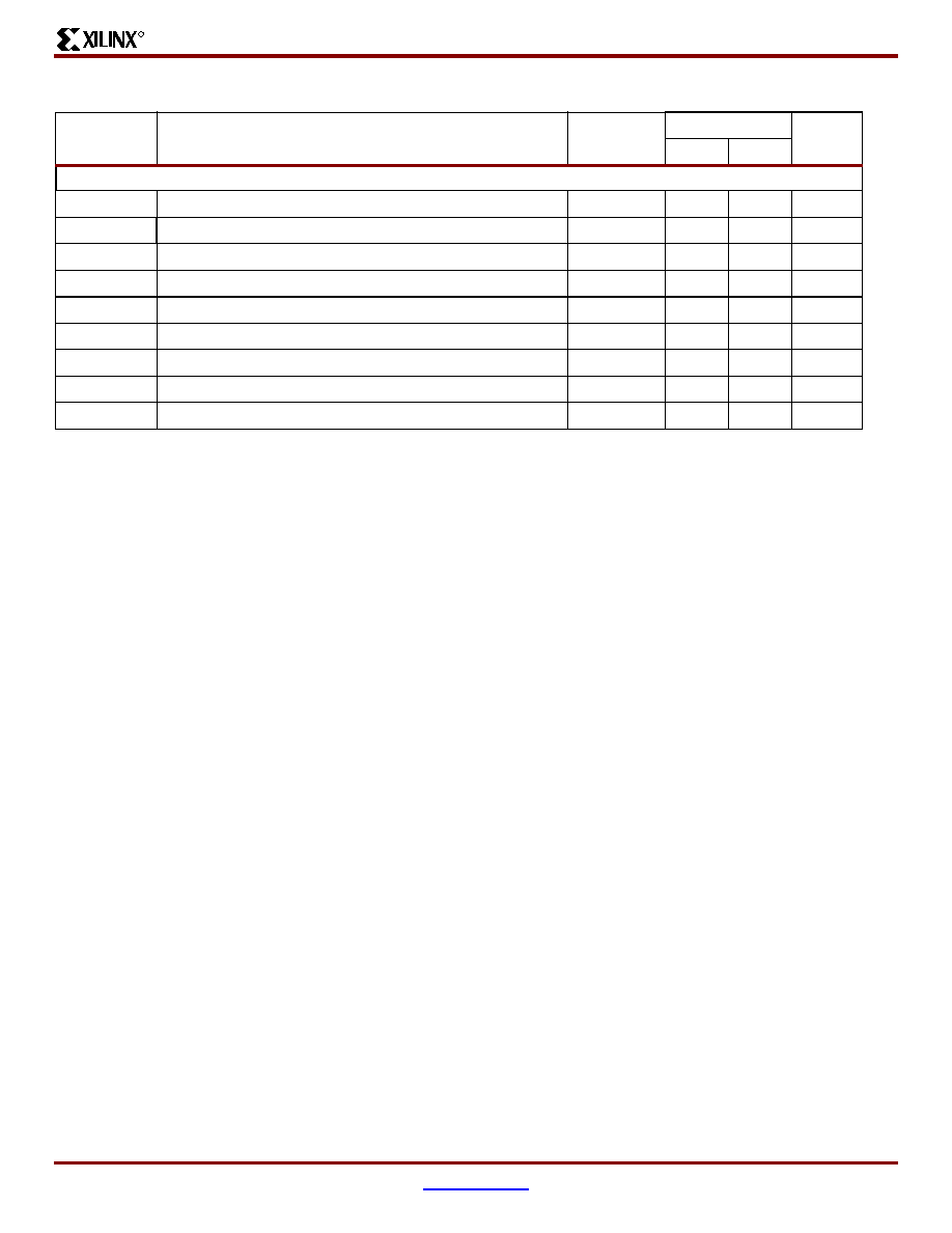
Table 1: XQR4000XL Series Radiation Hardened Field Programmable Gate Arrays
Device
Logic
Cells
Max.
Logic
Gates
(No RAM)
Max. RAM
Bits
(No Logic)
Typical
Gate Range
(Logic and
RAM)
(1)
CLB
Matrix
Total
CLBs
Number
of
Flip-Flops
Max.
User
I/O
Packages
XQR4013XL
1,368
13,000
18,432
10,000 - 30,000
24 x 24
576
1,536
192
CB228
XQR4036XL
3,078
36,000
41,472
22,000 - 65,000
36 x 36
1,296
3,168
288
CB228
XQR4062XL
5,472
62,000
73,728
40,000 - 130,000
48 x 48
2,304
5,376
384
CB228
Notes:
1.
Max values of Typical Gate Range include 20-30% of CLBs used as RAM.
QPRO XQR4000XL Radiation Hardened FPGAs
2
www.xilinx.com
DS071 (v1.1) June 25, 2000
1-800-255-7778
Product Specification
R
Radiation Specifications
Symbol
Description
Min
Max
Units
TID
Total ionizing dose
-
60K
RAD(Si)
SEL
Single event Latch-up LET> 100 MeV CM
2
/mg. @ +125∞C
-
0
SEU
Single event upset galactic p+
(1)
-
2.43E ≠ 8
Upsets/
Bit-Day
SEU
Single event upset galactic heavy Ion
(1)
-
9.54E ≠ 8
Upsets/
Bit-Day
SEU
Single event upset trapped p+
(1)
-
2.50E ≠ 7
Upsets/
Bit-Day
SEU
Single event upset galactic p+
(2)
-
5.62E ≠ 8
Upsets/
Bit-Day
SEU
Single event upset galactic heavy Ion
(2)
-
2.43E ≠ 7
Upsets/
Bit-Day
Notes:
1.
680 Km LEO, 98
o
Inclination, 100-mil Al Shielding
2.
35,000 Km GEO, 0
o
Inclination, 100-mil Al Shielding
3.
Simulations done using Space Radiation Version 2.5 code from Severn Communication Corp.
QPRO XQR4000XL Radiation Hardened FPGAs
DS071 (v1.1) June 25, 2000
www.xilinx.com
3
Product Specification
1-800-255-7778
R
XQR4000XL Switching Characteristics
Definition of Terms
In the following tables, some specifications may be designated as Advance or Preliminary. These terms are defined as
follows:
Advance:
Initial estimates based on simulation and/or extrapolation from other speed grades, devices, or
devicefamilies. Values are subject to change. Use as estimates, not for production.
Preliminary:
Based on preliminary characterization. Further changes are not expected.
Unmarked:
Specifications not identified as either Advance or Preliminary are to be considered Final.
Except for pin-to-pin input and output parameters, the AC parameter delay specifications included in this document are
derived from measuring internal test patterns. All specifications are representative of worst-case supply voltage and junction
temperature conditions.
All specifications subject to change without notice.
Additional Specifications
Except for pin-to-pin input and output parameters, the a.c.
parameter delay specifications included in this document
are derived from measuring internal test patterns. All speci-
fications are representative of worst-case supply voltage
and junction temperature conditions. The parameters
included are common to popular designs and typical appli-
cations. For design considerations requiring more detailed
timing information, see the appropriate family AC supple-
ments available on the Xilinx web site at:
http://www.xilinx.com/partinfo/databook.htm
.
Absolute Maximum Ratings
(1)
Recommended Operating Conditions
(1)
Symbol
Description
Units
V
CC
Supply voltage relative to GND
≠0.5 to 4.0
V
V
IN
Input voltage relative to GND
(2)
≠0.5 to 5.5
V
V
TS
Voltage applied to High-Z output
(2)
≠0.5 to 5.5
V
V
CCt
Longest supply voltage rise time from 1V to 3V
50
ms
T
STG
Storage temperature (ambient)
≠65 to +150
∞
C
T
SOL
Maximum soldering temperature (10s @ 1/16 in. = 1.5 mm)
+260
∞
C
T
J
Junction temperature
+150
∞
C
Notes:
1.
Stresses beyond those listed under Absolute Maximum Ratings may cause permanent damage to the device. These are stress
ratings only, and functional operation of the device at these or any other conditions beyond those listed under Operating Conditions
is not implied. Exposure to Absolute Maximum Ratings conditions for extended periods of time may affect device reliability.
2.
Maximum DC overshoot or undershoot above V
CC
or below GND must be limited to either 0.5V or 10 mA, whichever is easier to
achieve. During transitions, the device pins may undershoot to ≠2.0 V or overshoot to V
CC
+ 2.0V, provided this over- or undershoot
lasts less than 10 ns and with the forcing current being limited to 200 mA.
Symbol
Description
Min
Max
Units
V
CC
Supply voltage relative to GND, T
C
= ≠55
∞
C to +125
∞
C
3.0
3.6
V
V
IH
High-level input voltage
(2)
50% of V
CC
5.5
V
V
IL
Low-level input voltage
0
30% of V
CC
V
T
IN
Input signal transition time
-
250
ns
Notes:
1.
At junction temperatures above those listed as Operating Conditions, all delay parameters increase by 0.35% per ∞C.
2.
Input and output measurement threshold is ~50% of V
CC
.
QPRO XQR4000XL Radiation Hardened FPGAs
4
www.xilinx.com
DS071 (v1.1) June 25, 2000
1-800-255-7778
Product Specification
R
XQR4000XL DC Characteristics Over Recommended Operating Conditions
Power-On Power Supply Requirements
Xilinx FPGAs require a minimum rated power supply current
capacity to insure proper initialization, and the power supply
ramp-up time does affect the current required. A fast
ramp-up time requires more current than a slow ramp-up
time. The slowest ramp-up time is 50 ms. Current capacity
is not specified for a ramp-up time faster than 2 ms. The cur-
rent capacity varies linealy with ramp-up time, e.g., an
XQR4036XL with a ramp-up time of 25 ms would require a
capacity predicted by the point on the straight line drawn
from 1A at 120
µ
s to 500 mA at 50 ms at the 25 ms time
mark. This point is approximately 750 mA
.
Symbol
Description
Min
Max
Units
V
OH
High-level output voltage at I
OH
= ≠4 mA, V
CC
min (LVTTL)
2.4
-
V
High-level output voltage at I
OH
= ≠500
µ
A, (LVCMOS)
90% V
CC
-
V
V
OL
Low-level output voltage at I
OL
= 12 mA, V
CC
min (LVTTL)
(1)
-
0.4
V
Low-level output voltage at I
OL
= 1500
µ
A, (LVCMOS)
-
10% V
CC
V
V
DR
Data retention supply voltage (below which configuration data may be lost)
2.5
-
V
I
CCO
Quiescent FPGA supply current
(2)
-
5
mA
I
L
Input or output leakage current
≠10
+10
µ
A
C
IN
Input capacitance (sample tested)
-
10
pF
I
RPU
Pad pull-up (when selected) at V
IN
= 0V (sample tested)
0.02
0.25
mA
I
RPD
Pad pull-down (when selected) at V
IN
= 3.6V (sample tested)
0.02
0.15
mA
I
RLL
Horizontal longline pull-up (when selected) at logic Low
0.3
2.0
mA
Notes:
1.
With up to 64 pins simultaneously sinking 12 mA.
2.
With no output current loads, no active input or Longline pull-up resistors, all I/O pins in a High-Z state and floating.
Product
Description
Ramp-up Time
Fast (120
µ
s)
Slow (50 ms)
XQR4013 - 36XL
Minimum required current supply
1A
500 mA
XC4062XL
Minimum required current supply
2A
500 mA
Notes:
1.
Devices are guaranteed to initialize properly with the minimum current listed above. A larger capacity power supply may result in a
larger initialization current.
2.
This specification applies to Commercial and Industrial grade products only.
3.
Ramp-up Time is measured from 0V
DC
to 3.6V
DC
. Peak current required lasts less than 3 ms, and occurs near the internal power
on reset threshold voltage. After initialization and before configuration, I
CC
max is less than 10 mA.
QPRO XQR4000XL Radiation Hardened FPGAs
DS071 (v1.1) June 25, 2000
www.xilinx.com
5
Product Specification
1-800-255-7778
R
XQR4000XL AC Switching Characteristic
Testing of the switching parameters is modeled after testing
methods specified by MIL-M-38510/605. All devices are
100% functionally tested. Internal timing parameters are
derived from measuring internal test patterns. Listed below
are representative values where one global clock input
drives one vertical clock line in each accessible column, and
where all accessible IOB and CLB flip-flops are clocked by
the global clock net.
When fewer vertical clock lines are connected, the clock dis-
tribution is faster; when multiple clock lines per column are
driven from the same global clock, the delay is longer. For
more specific, more precise, and worst-case guaranteed
data, reflecting the actual routing structure, use the values
provided by the static timing analyzer (TRCE in the Xilinx
Development System) and back-annotated to the simulation
netlist. These path delays, provided as a guideline, have
been extracted from the static timing analyzer report. All
timing parameters assume worst-case operating conditions
(supply voltage and junction temperature)
Global Buffer Switching Characteristics
Global Early BUFGEs 1, 2, 5, and 6 to IOB Clock Characteristics
Global Early BUFGEs 3, 4, 7, and 8 to IOB Clock Characteristics
Symbol
Description
Device
-3
Units
Min
Max
T
GLS
Delay from pad through Global Low Skew buffer, to any
clock K
XQR4013XL
0.6
3.6
ns
XQR4036XL
1.1
4.8
ns
XQR4062XL
1.4
6.3
ns
Symbol
Description
Device
-3
Units
Min
Max
T
GE
Delay from pad through Global Early buffer, to any IOB
clock. Values are for BUFGEs 1, 2, 5 and 6.
XQR4013XL
0.4
2.4
ns
XQR4036XL
0.3
3.1
ns
XQR4062XL
0.3
4.9
ns
Symbol
Description
Device
-3
Units
Min
Max
T
GE
Delay from pad through Global Early buffer, to any IOB
clock. Values are for BUFGEs 3, 4, 7 and 8.
XQR4013XL
0.7
2.4
ns
XQR4036XL
0.9
4.7
ns
XQR4062XL
1.2
5.9
ns
QPRO XQR4000XL Radiation Hardened FPGAs
6
www.xilinx.com
DS071 (v1.1) June 25, 2000
1-800-255-7778
Product Specification
R
XQR4000XL CLB Switching Characteristic Guidelines
Testing of switching parameters is modeled after testing
methods specified by MIL-M-38510/605. All devices are
100% functionally tested. Internal timing parameters are
derived from measuring internal test patterns. Listed below
are representative values. For more specific, more precise,
and worst-case guaranteed data, use the values reported
by the static timing analyzer (TRCE in the Xilinx Develop-
ment System) and back-annotated to the simulation netlist.
All timing parameters assume worst-case operating condi-
tions (supply voltage and junction temperature). Values
apply to all XQR4000XL devices and expressed in nano-
seconds unless otherwise noted.
CLB Switching Characteristics
Symbol
Description
-3
Units
Min
Max
Combinatorial Delays
T
ILO
F/G inputs to X/Y outputs
-
1.6
ns
T
IHO
F/G inputs via H' to X/Y outputs
-
2.7
ns
T
ITO
F/G inputs via transparent latch to Q outputs
-
2.9
ns
T
HH0O
C inputs via SR/H0 via H to X/Y outputs
-
2.5
ns
T
HH1O
C inputs via H1 via H to X/Y outputs
-
2.4
ns
T
HH2O
C inputs via D
IN
/H2 via H to X/Y outputs
-
2.5
ns
T
CBYP
C inputs via EC, D
IN
/H2 to YQ, XQ output (bypass)
-
1.5
ns
CLB Fast Carry Logic
T
OPCY
Operand inputs (F1, F2, G1, G4) to C
OUT
-
2.7
ns
T
ASCY
Add/subtract input (F3) to C
OUT
-
3.3
ns
T
INCY
Initialization inputs (F1, F3) to C
OUT
-
2.0
ns
T
SUM
C
IN
through function generators to X/Y outputs
-
2.8
ns
T
BYP
C
IN
to C
OUT
, bypass function generators
-
0.26
ns
T
NET
Carry net delay, C
OUT
to C
IN
-
0.32
ns
Sequential Delays
T
CKO
Clock K to flip-flop outputs Q
-
2.1
ns
T
CKLO
Clock K to latch outputs Q
-
2.1
ns
Setup Time Before Clock K
T
ICK
F/G inputs
1.1
-
ns
T
IHCK
F/G inputs via H
2.2
-
ns
T
HH0CK
C inputs via H0 through H
2.0
-
ns
T
HH1CK
C inputs via H1 through H
1.9
-
ns
T
HH2CK
C inputs via H2 through H
2.0
-
ns
T
DICK
C inputs via D
IN
0.9
-
ns
T
ECCK
C inputs via EC
1.0
-
ns
T
RCK
C inputs via S/R, going Low (inactive)
0.6
-
ns
T
CCK
C
IN
input via F/G
2.3
-
ns
T
CHCK
C
IN
input via F/G and H
3.4
-
ns
QPRO XQR4000XL Radiation Hardened FPGAs
DS071 (v1.1) June 25, 2000
www.xilinx.com
7
Product Specification
1-800-255-7778
R
Hold Time After Clock K
T
CKI
F/G inputs
0
-
ns
T
CKIH
F/G inputs via H
0
-
ns
T
CKHH0
C inputs via SR/H0 through H
0
-
ns
T
CKHH1
C inputs via H1 through H
0
-
ns
T
CKHH2
C inputs via D
IN
/H2 through H
0
-
ns
T
CKDI
C inputs via D
IN
/H2
0
-
ns
T
CKEC
C inputs via EC
0
-
ns
T
CKR
C inputs via SR, going Low (inactive)
0
-
ns
Clock
T
CH
Clock High time
3.0
-
ns
T
CL
Clock Low time
3.0
-
ns
Set/Reset Direct
T
RPW
Width (High)
3.0
-
ns
T
RIO
Delay from C inputs via S/R, going High to Q
-
3.7
ns
Global Set/Reset
T
MRW
Minimum GSR pulse width
-
19.8
ns
T
MRQ
Delay from GSR input to any Q
See
page 16
for T
RRI
values per device.
F
TOG
Toggle frequency (MHz) (for export control)
-
166
MHz
CLB Switching Characteristics (Continued)
Symbol
Description
-3
Units
Min
Max
QPRO XQR4000XL Radiation Hardened FPGAs
8
www.xilinx.com
DS071 (v1.1) June 25, 2000
1-800-255-7778
Product Specification
R
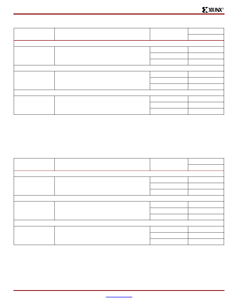
XQR4000XL RAM Synchronous (Edge-Triggered) Write Operation Guidelines
Testing of switching parameters is modeled after testing
methods specified by MIL-M-38510/605. All devices are
100% functionally tested. Internal timing parameters are
derived from measuring internal test patterns. Listed below
are representative values. For more specific, more precise,
and worst-case guaranteed data, use the values reported
by the static timing analyzer (TRCE in the Xilinx Develop-
ment System) and back-annotated to the simulation netlist.
All timing parameters assume worst-case operating condi-
tions (supply voltage and junction temperature). Values
apply to all XQR4000XL devices and are expressed in
nanoseconds unless otherwise noted.
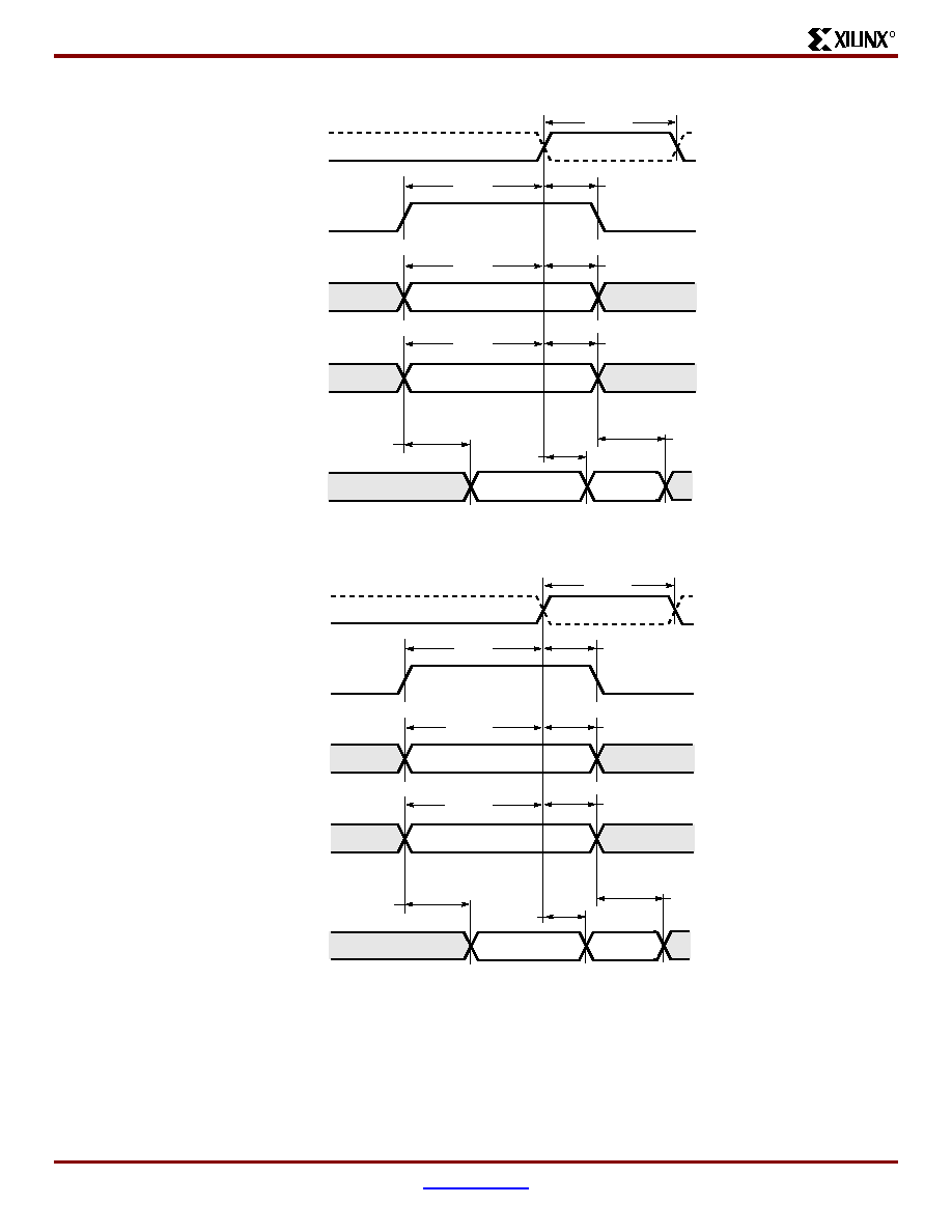
Single-Port RAM Synchronous (Edge-Triggered) Write Operation Characteristics
Symbol
Single Port RAM
Size
-3
Units
Min
Max
Write Operation
T
WCS
Address write cycle time (clock K period)
16x2
9.0
-
ns
T
WCTS
32x1
9.0
-
ns
T
WPS
Clock K pulse width (active edge)
16x2
4.5
-
ns
T
WPTS
32x1
4.5
-
ns
T
ASS
Address setup time before clock K
16x2
2.2
-
ns
T
ASTS
32x1
2.2
-
ns
T
AHS
Address hold time after clock K
16x2
0
-
ns
T
AHTS
32x1
0
-
ns
T
DSS
D
IN
setup time before clock K
16x2
2.0
-
ns
T
DSTS
32x1
2.5
-
ns
T
DHS
D
IN
hold time after clock K
16x2
0
-
ns
T
DHTS
32x1
0
-
ns
T
WSS
WE setup time before clock K
16x2
2.0
-
ns
T
WSTS
32x1
1.8
-
ns
T
WHS
WE hold time after clock K
16x2
0
-
ns
T
WHTS
32x1
0
-
ns
T
WOS
Data valid after clock K
16x2
-
6.8
ns
T
WOTS
32x1
-
8.1
ns
Read Operation
T
RC
Address read cycle time
16x2
4.5
-
ns
T
RCT
32x1
6.5
-
ns
T
ILO
Data valid after address change (no Write Enable)
16x2
-
1.6
ns
T
IHO
32x1
-
2.7
ns
T
ICK
Address setup time before clock K
16x2
1.1
-
ns
T
IHCK
32x1
2.2
-
ns
QPRO XQR4000XL Radiation Hardened FPGAs
DS071 (v1.1) June 25, 2000
www.xilinx.com
9
Product Specification
1-800-255-7778
R
Dual-Port RAM Synchronous (Edge-Triggered) Write Operation Characteristics
Symbol
Dual Port RAM
Size
-3
Units
Min
Max
Write Operation
T
WCDS
Address write cycle time (clock K period)
16x1
9.0
ns
T
WPDS
Clock K pulse width (active edge)
16x1
4.5
-
ns
T
ASDS
Address setup time before clock K
16x1
2.5
-
ns
T
AHDS
Address hold time after clock K
16x1
0
-
ns
T
DSDS
D
IN
setup time before clock K
16x1
2.5
-
ns
T
DHDS
D
IN
hold time after clock K
16x1
0
-
ns
T
WSDS
WE setup time before clock K
16x1
1.8
-
ns
T
WHDS
WE hold time after clock K
16x1
0
-
ns
T
WODS
Data valid after clock K
16x1
-
7.8
ns
QPRO XQR4000XL Radiation Hardened FPGAs
10
www.xilinx.com
DS071 (v1.1) June 25, 2000
1-800-255-7778
Product Specification
R
XQR4000XL CLB Single-Port RAM Synchronous (Edge-Triggered) Write Timing
XQR4000XL CLB Dual-Port RAM Synchronous (Edge-Triggered) Write Timing
DS029_01_011300
WCLK (K)
WE
ADDRESS
DATA IN
DATA OUT
OLD
NEW
T
DSS
T
DHS
T
ASS
T
AHS
T
WSS
T
WPS
T
WHS
T
WOS
T
ILO
T
ILO
DS029_02_011300
WCLK (K)
WE
ADDRESS
DATA IN
DATA OUT
OLD
NEW
T
DSDS
T
DHDS
T
ASDS
T
AHDS
T
WSS
T
WPDS
T
WHS
T
WODS
T
ILO
T
ILO
QPRO XQR4000XL Radiation Hardened FPGAs
DS071 (v1.1) June 25, 2000
www.xilinx.com
11
Product Specification
1-800-255-7778
R
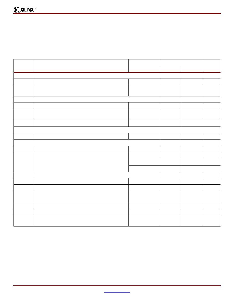
XQR4000XL Pin-to-Pin Output Parameter Guidelines
Testing of switching parameters is modeled after testing
methods specified by MIL-M-38510/605. All devices are
100% functionally tested. Pin-to-pin timing parameters are
derived from measuring external and internal test patterns
and are guaranteed over worst-case operating conditions
(supply voltage and junction temperature). Listed below are
representative values for typical pin locations and normal
clock loading. For more specific, more precise, and
worst-case guaranteed data, reflecting the actual routing
structure, use the values provided by the static timing ana-
lyzer (TRCE in the Xilinx Development System) and
back-annotated to the simulation netlist. These path delays,
provided as a guideline, have been extracted from the static
timing analyzer report. Values are expressed in nanosec-
onds unless otherwise noted.
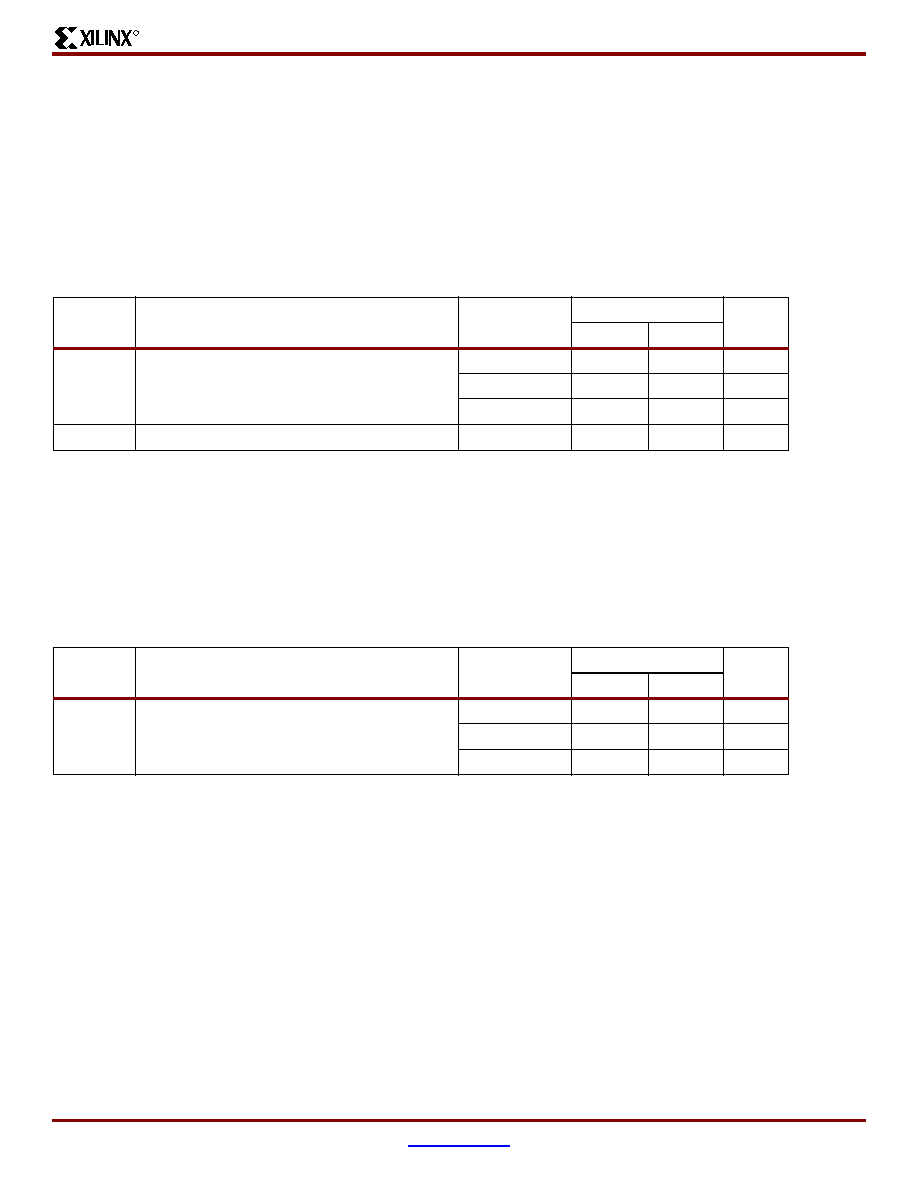
Output Flip-Flop, Clock to Out
(1,2,3)
Output Flip-Flop, Clock to Out, BUFGEs 1, 2, 5, and 6
Symbol
Description
Device
-3
Units
Min
Max
T
ICKOF
Global low skew clock to output using OFF
(4)
XQR4013XL
1.5
8.6
ns
XQR4036XL
2.0
9.8
ns
XQR4062XL
2.3
11.3
ns
T
SLOW
For output SLOW option add
All Devices
3.0
3.0
ns
Notes:
1.
Listed above are representative values where one global clock input drives one vertical clock line in each accessible
column, and where all accessible IOB and CLB flip-flops are clocked by the global clock net.
2.
Clock-to-out minimum delay is measured with the fastest route and the lightest load, Clock-to-out maximum delay is
measured using the farthest distance and a reference load of one clock pin (IK or OK) per IOB as well as driving all
accessible CLB flip-flops. For designs with a smaller number of clock loads, the pad-to-IOB clock pin delay as
determined by the static timing analyzer (TRCE) can be added to the AC parameter Tokpof and used as a worst-case
pin-to-pin clock-to-out delay for clocked outputs for FAST mode configurations.
3.
Output timing is measured at ~50% V
CC
threshold with 50 pF external capacitive load.
4.
OFF = Output Flip-Flop
Symbol
Description
Device
-3
Units
Min
Max
T
ICKEOF
Global early clock to output using OFF
Values are for BUFGEs 1, 2, 5, and 6.
XQR4013XL
1.3
7.4
ns
XQR4036XL
1.2
8.1
ns
XQR4062XL
1.2
9.9
ns
Notes:
1.
Clock-to-out minimum delay is measured with the fastest route and the lightest load, Clock-to-out maximum delay is
measured using the farthest distance and a reference load of one clock pin (IK or OK) per IOB as well as driving all
accessible CLB flip-flops. For designs with a smaller number of clock loads, the pad-to-IOB clock pin delay as
determined by the static timing analyzer (TRCE) can be added to the AC parameter T
OKPOF
and used as a worst-case
pin-to-pin clock-to-out delay for clocked outputs for FAST mode configurations.
2.
Output timing is measured at ~50% V
CC
threshold with 50 pF external capacitive load.

QPRO XQR4000XL Radiation Hardened FPGAs
12
www.xilinx.com
DS071 (v1.1) June 25, 2000
1-800-255-7778
Product Specification
R
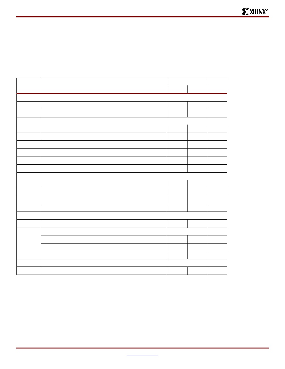
Output Flip-Flop, Clock to Out, BUFGEs 3, 4, 7, and 8
Capacitive Load Factor
Figure 1
shows the relationship between I/O output delay
and load capacitance. It allows a user to adjust the specified
output delay if the load capacitance is different than 50 pF.
For example, if the actual load capacitance is 120 pF, add
2.5 ns to the specified delay. If the load capacitance is
20 pF, subtract 0.8 ns from the specified output delay.
Figure 1
is usable over the specified operating conditions of
voltage and temperature and is independent of the output
slew rate control.
Symbol
Description
Device
-3
Units
Min
Max
T
ICKEOF
Global early clock to output using OFF
Values are for BUFGEs 3, 4, 7, and 8.
XQR4013XL
1.8
8.8
ns
XQR4036XL
1.8
9.7
ns
XQR4062XL
2.0
10.9
ns
Notes:
1.
Clock-to-out minimum delay is measured with the fastest route and the lightest load, Clock-to-out maximum delay is
measured using the farthest distance and a reference load of one clock pin (IK or OK) per IOB as well as driving all
accessible CLB flip-flops. For designs with a smaller number of clock loads, the pad-to-IOB clock pin delay as
determined by the static timing analyzer (TRCE) can be added to the AC parameter T
OKPOF
and used as a worst-case
pin-to-pin clock-to-out delay for clocked outputs for FAST mode configurations.
2.
Output timing is measured at ~50% V
CC
threshold with 50 pF external capacitive load.
Figure 1: Delay Factor at Various Capacitive Loads
DS029_03_011300
-2
0
20
40
60
80
Capacitance (pF)
Delta Dela
y (ns)
100
120
140
-1
0
1
2
3
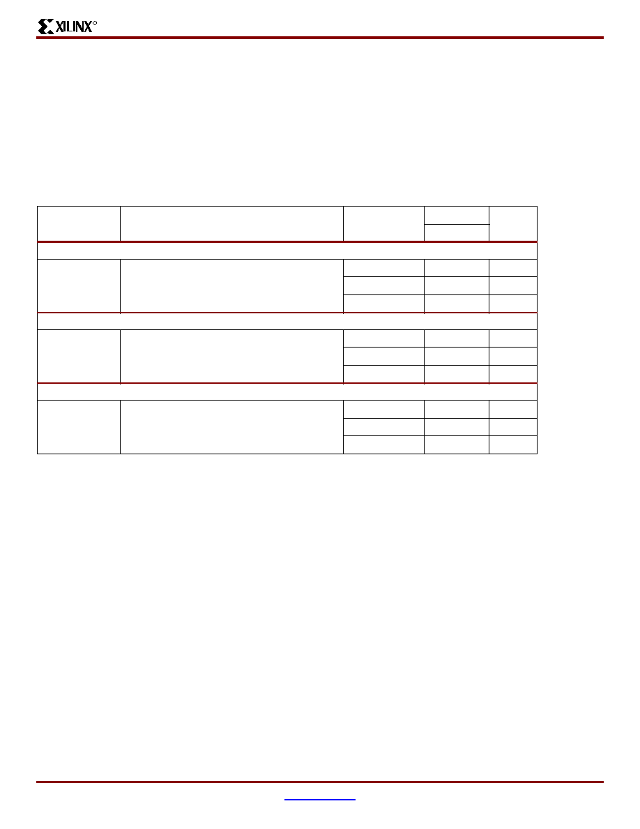
QPRO XQR4000XL Radiation Hardened FPGAs
DS071 (v1.1) June 25, 2000
www.xilinx.com
13
Product Specification
1-800-255-7778
R
XQR4000XL Pin-to-Pin Input Parameter Guidelines
Testing of switching parameters is modeled after testing
methods specified by MIL-M-38510/605. All devices are
100% functionally tested. Pin-to-pin timing parameters are
derived from measuring external and internal test patterns
and are guaranteed over worst-case operating conditions
(supply voltage and junction temperature). Listed below are
representative values for typical pin locations and normal
clock loading. For more specific, more precise, and
worst-case guaranteed data, reflecting the actual routing
structure, use the values provided by the static timing ana-
lyzer (TRCE in the Xilinx Development System) and
back-annotated to the simulation netlist. These path delays,
provided as a guideline, have been extracted from the static
timing analyzer report. Values are expressed in nanosec-
onds unless otherwise noted.
Global Low Skew Clock, Input Setup and Hold Times
(1,2)
Symbol
Description
Device
(1)
-3
Units
Min
No Delay
T
PSN
/T
PHN
Global early clock and IFF
(3)
Global early clock and FCL
(4)
XQR4013XL
1.2 / 3.2
ns
XQR4036XL
1.2 / 5.5
ns
XQR4062XL
1.2 / 7.0
ns
Partial Delay
T
PSP
/T
PHP
Global early clock and IFF
(3)
Global early clock and FCL
(4)
XQR4013XL
6.1 / 0.0
ns
XQR4036XL
6.4 / 1.0
ns
XQR4062XL
6.7 / 1.2
ns
Full Delay
T
PSD
/T
PHD
Global early clock and IFF
(3)
XQR4013XL
6.4 / 0.0
ns
XQR4036XL
6.6 / 0.0
ns
XQR4062XL
6.8 / 0.0
ns
Notes:
1.
The XQR4013XL, XQR4036XL, and XQR4062XL have significantly faster partial and full delay setup times than
other devices.
2.
Input setup time is measured with the fastest route and the lightest load. Input hold time is measured using the
furthest distance and a reference load of one clock pin per IOB as well as driving all accessible CLB flip-flops. For
designs with a smaller number of clock loads, the pad-to-IOB clock pin delay as determined by the static timing
analyzer (TRCE) can be used as a worst-case pin-to-pin no-delay input hold specification.
3.
IFF = Input Flip-Flop or Latch
4.
FCL = Fast Capture Latch
QPRO XQR4000XL Radiation Hardened FPGAs
14
www.xilinx.com
DS071 (v1.1) June 25, 2000
1-800-255-7778
Product Specification
R
Global Early Clock BUFEs 1, 2, 5, and 6 Setup and Hold for IFF and FCL
(1,2)
Global Early Clock BUFEs 3, 4, 7, and 8 Setup and Hold for IFF and FCL
(1,2)
Symbol
Description
Device
-3
Min
No Delay
T
PSEN
/T
PHEN
T
PFSEN
/T
PFHEN
Global early clock and IFF
(3)
Global early clock and FCL
(4)
XQR4013XL
1.2 / 4.7
XQR4036XL
1.2 / 6.7
XQR4062XL
1.2 / 8.4
Partial Delay
T
PSEPN
/T
PHEP
T
PFSEP
/T
PFHEP
Global early clock and IFF
(3)
Global early clock and FCL
(4)
XQR4013XL
6.4 / 0.0
XQR4036XL
7.0 / 0.8
XQR4062XL
9.0 / 0.8
Full Delay
T
PSEPD
/T
PHED
Global early clock and IFF
(3)
XQR4013XL
12.0 / 0.0
XQR4036XL
13.8 / 0.0
XQR4062XL
13.1 / 0.0
Notes:
1.
The XQR4013XL, XQR4036XL, and XQR4062XL have significantly faster partial and full delay setup times than other devices.
2.
Input setup time is measured with the fastest route and the lightest load. Input hold time is measured using the furthest distance and
a reference load of one clock pin per IOB as well as driving all accessible CLB flip-flops. For designs with a smaller number of clock
loads, the pad-to-IOB clock pin delay as determined by the static timing analyzer (TRCE) can be used as a worst-case pin-to-pin
no-delay input hold specification.
3.
IFF = Input Flip-Flop or Latch
4.
FCL = Fast Capture Latch
Symbol
Description
Device
-3
Min
No Delay
T
PSEN
/T
PHEN
T
PFSEN
/T
PFHEN
Global early clock and IFF
(3)
Global early clock and FCL
(4)
XQR4013XL
1.2 / 4.7
XQR4036XL
1.2 / 6.7
XQR4062XL
1.2 / 8.4
Partial Delay
T
PSEPN
/T
PHEP
T
PFSEP
/T
PFHEP
Global early clock and IFF
(3)
Global early clock and FCL
(4)
XQR4013XL
5.4 / 0.0
XQR4036XL
6.4 / 0.8
XQR4062XL
8.4 / 1.5
Full Delay
T
PSEPD
/T
PHED
Global early clock and IFF
(3)
XQR4013XL
10.0 / 0.0
XQR4036XL
12.2 / 0.0
XQR4062XL
13.1 / 0.0
Notes:
1.
The XQR4013XL, XQR4036XL, and XQR4062XL have significantly faster partial and full delay setup times than other devices.
2.
Input setup time is measured with the fastest route and the lightest load. Input hold time is measured using the furthest distance and
a reference load of one clock pin per IOB as well as driving all accessible CLB flip-flops. For designs with a smaller number of clock
loads, the pad-to-IOB clock pin delay as determined by the static timing analyzer (TRCE) can be used as a worst-case pin-to-pin
no-delay input hold specification.
3.
IFF = Input Flip-Flop or Latch
4.
FCL = Fast Capture Latch
QPRO XQR4000XL Radiation Hardened FPGAs
DS071 (v1.1) June 25, 2000
www.xilinx.com
15
Product Specification
1-800-255-7778
R
XQR4000XL IOB Input Switching Characteristic Guidelines
Testing of switching parameters is modeled after testing
methods specified by MIL-M-38510/605. All devices are
100% functionally tested. Internal timing parameters are
derived from measuring internal test patterns. Listed below
are representative values. For more specific, more precise,
and worst-case guaranteed data, use the values reported
by the static timing analyzer (TRCE in the Xilinx Develop-
ment System) and back-annotated to the simulation netlist.
These path delays, provided as a guideline, have been
extracted from the static timing analyzer report. All timing
parameters assume worst-case operating conditions (sup-
ply voltage and junction temperature)
.
Symbol
Description
Device
-3
Units
Min
Max
Clocks
T
ECIK
Clock enable (EC) to clock (IK)
All devices
0.1
-
ns
T
OKIK
Delay from FCL enable (OK) active edge to IFF clock
(IK) active edge
All devices
2.2
-
ns
Setup Times
T
PICK
Pad to clock (IK), no delay
All devices
1.7
-
ns
T
PICKF
Pad to clock (IK), via transparent fast capture latch, no
delay
All devices
2.3
-
ns
T
POCK
Pad to fast capture latch enable (OK), no delay
All devices
1.2
-
ns
Hold Times
All Hold Times
All devices
0
-
ns
Global Set/Reset
T
MRW
Minimum GSR pulse width
All devices
-
19.8
ns
T
RRI
Delay from GSR input to any Q
(2)
XQR4013XL
-
15.9
ns
XQR4036XL
-
22.5
ns
XQR4062XL
-
29.1
ns
Propagation Delays
T
PID
Pad to I1, I2
All devices
-
1.6
ns
T
PLI
Pad to I1, I2 via transparent input latch, no delay
All devices
-
3.1
ns
T
PFLI
Pad to I1, I2 via transparent FCL and input latch, no
delay
All devices
-
3.7
ns
T
IKRI
Clock (IK) to I1, I2 (flip-flop)
All devices
-
1.7
ns
T
IKLI
Clock (IK) to I1, I2 (latch enable, active Low)
All devices
-
1.8
ns
T
OKLI
FCL enable (OK) active edge to I1, I2
(via transparent standard input latch)
All devices
-
3.6
ns
Notes:
1.
IFF = Input Flip-Flop or Latch, FCL = Fast Capture Latch
2.
Indicates Minimum Amount of Time to Assure Valid Data.
QPRO XQR4000XL Radiation Hardened FPGAs
16
www.xilinx.com
DS071 (v1.1) June 25, 2000
1-800-255-7778
Product Specification
R
XQR4000XL IOB Output Switching Characteristic Guidelines
Testing of switching parameters is modeled after testing
methods specified by MIL-M-38510/605. All devices are
100% functionally tested. Internal timing parameters are
derived from measuring internal test patterns. Listed below
are representative values. For more specific, more precise,
and worst-case guaranteed data, use the values reported
by the static timing analyzer (TRCE in the Xilinx Develop-
ment System) and back-annotated to the simulation netlist.
These path delays, provided as a guideline, have been
extracted from the static timing analyzer report. All timing
parameters assume worst-case operating conditions (sup-
ply voltage and junction temperature). For Propagation
Delays, slew-rate = fast unless otherwise noted. Values are
expressed in nanoseconds unless otherwise noted.
Symbol
Description
-3
Units
Min
Max
Clocks
T
CH
Clock High
3.0
-
ns
T
CL
Clock Low
3.0
-
ns
Propagation Delays
T
OKPOF
Clock (OK) to pad
-
5.0
ns
T
OPF
Output (O) to pad
-
4.1
ns
T
TSHZ
High-Z to pad High-Z (slew-rate independent)
-
4.4
ns
T
TSONF
High-Z to pad active and valid
-
4.1
ns
T
OFPF
Output (O) to pad via fast output MUX
-
5.5
ns
T
OKFPF
Select (OK) to pad via fast MUX
-
5.1
ns
Setup and Hold Times
T
OOK
Output (O) to clock (OK) setup time
0.5
-
ns
T
OKO
Output (O) to clock (OK) hold time
0
-
ns
T
ECOK
Clock Enable (EC) to clock (OK) setup time
0
-
ns
T
OKEC
Clock Enable (EC) to clock (OK) hold time
0.3
-
ns
Global Set/Reset
T
MRW
Minimum GSR pulse width
19.8
-
ns
T
RPO
Delay from GSR input to any pad
(2)
XQR4013XL
-
20.5
ns
XQR4036XL
-
27.1
ns
XQR4062XL
-
33.7
ns
Slew Rate Adjustment
T
SLOW
For output SLOW option add
-
3.0
ns
Notes:
1.
Output timing is measured at ~50% V
CC
threshold, with 50 pF external capacitive loads.
2.
Indicates Minimum Amount of Time to Assure Valid Data.
QPRO XQR4000XL Radiation Hardened FPGAs
DS071 (v1.1) June 25, 2000
www.xilinx.com
17
Product Specification
1-800-255-7778
R
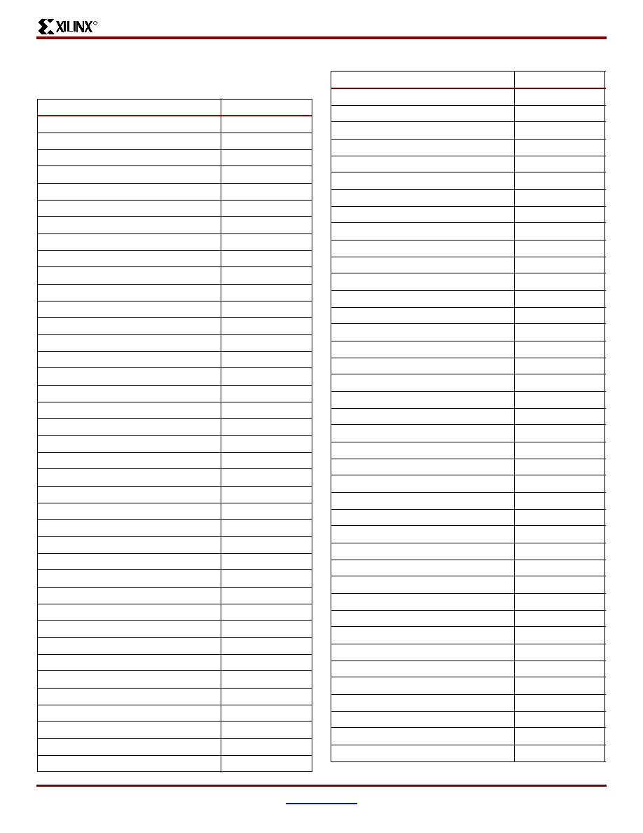
Pinouts
CB228 Package for XQR4013XL/4036XL/4062XL
Pin Name
CB228
GND
P1
BUFGP_TL_A16_GCK1_IO
P2
A17_IO
P3
IO
P4
IO
P5
TDI_IO
P6
TCK_IO
P7
IO
P8
IO
P9
IO
P10
IO
P11
IO
P12
IO
P13
GND
P14
IO_FCLK1
P15
IO
P16
TMS_IO
P17
IO
P18
IO
P19
IO
P20
IO
P21
IO
P22
IO
P23
IO
P24
IO
P25
IO
P26
GND
P27
VCC
P28
IO
P29
IO
P30
IO
P31
IO
P32
IO
P33
IO
P34
IO
P35
IO
P36
VCC
P37
IO
P38
IO
P39
IO
P40
IO_FCKL2
P41
GND
P42
IO
P43
IO
P44
IO
P45
IO
P46
IO
P47
IO
P48
IO
P49
IO
P50
IO
P51
IO
P52
IO
P53
BUFGS_BL_GCK2_IO
P54
M1
P55
GND
P56
M0
P57
VCC
P58
M2
P59
BUFGP_BL_GCK3_IO
P60
HDC_IO
P61
IO
P62
IO
P63
IO
P64
LDC_IO
P65
IO
P66
IO
P67
IO
P68
IO
P69
IO
P70
IO
P71
GND
P72
IO
P73
IO
P74
IO
P75
IO
P76
IO
P77
IO
P78
IO
P79
CB228 Package for XQR4013XL/4036XL/4062XL
Pin Name
CB228
QPRO XQR4000XL Radiation Hardened FPGAs
18
www.xilinx.com
DS071 (v1.1) June 25, 2000
1-800-255-7778
Product Specification
R
IO
P80
IO
P81
IO
P82
IO
P83
/ERR_INIT_IO
P84
VCC
P85
GND
P86
IO
P87
IO
P88
IO
P89
IO
P90
IO
P91
IO
P92
IO
P93
IO
P94
VCC
P95
IO
P96
IO
P97
IO
P98
IO
P99
GND
P100
IO
P101
IO
P102
IO
P103
IO
P104
IO
P105
IO
P106
IO
P107
IO
P108
IO
P109
IO
P110
IO
P111
BUFGS_BR_GCK4_IO
P112
GND
P113
DONE
P114
VCC
P115
/PROG
P116
D7_IO
P117
BUFGP_BR_GCK5_IO
P118
IO
P119
CB228 Package for XQR4013XL/4036XL/4062XL
Pin Name
CB228
IO
P120
IO
P121
IO
P122
D6_IO
P123
IO
P124
IO
P125
IO
P126
IO
P127
IO
P128
GND
P129
IO
P130
IO
P131
IO
P132
IO
P133
D5_IO
P134
/CS0_IO
P135
IO
P136
IO
P137
IO
P138
IO
P139
D4_IO
P140
IO
P141
VCC
P142
GND
P143
D3_IO
P144
/RS_IO
P145
IO
P146
IO
P147
IO
P148
IO
P149
D2_IO
P150
IO
P151
VCC
P152
IO
P153
IO
P154
IO
P155
IO
P156
GND
P157
IO
P158
IO
P159
CB228 Package for XQR4013XL/4036XL/4062XL
Pin Name
CB228
QPRO XQR4000XL Radiation Hardened FPGAs
DS071 (v1.1) June 25, 2000
www.xilinx.com
19
Product Specification
1-800-255-7778
R
IO
P160
IO
P161
IO
P162
IO
P163
D1_IO
P164
BUSY_/RDY_RCLK_IO
P165
IO
P166
IO
P167
D0_DIN_IO
P168
BUFGS_TR_GCK6_DOUT_IO
P169
CCLK
P170
VCC
P171
TDO
P172
GND
P173
A0_/WS_IO
P174
BUFGP_TR_GCK7_A1_IO
P175
IO
P176
IO
P177
CSI_A2_IO
P178
A3_IO
P179
IO
P180
IO
P181
IO
P182
IO
P183
IO
P184
IO
P185
GND
P186
IO
P187
IO
P188
IO
P189
IO
P190
VCC
P191
A4_IO
P192
A5_IO
P193
IO
P194
IO
P195
A21_IO
P196
A20_IO
P197
A6_IO
P198
A7_IO
P199
CB228 Package for XQR4013XL/4036XL/4062XL
Pin Name
CB228
GND
P200
VCC
P201
A8_IO
P202
A9_IO
P203
A19_IO
P204
A18_IO
P205
IO
P206
IO
P207
A10_IO
P208
A11_IO
P209
VCC
P210
IO
P211
IO
P212
IO
P213
IO
P214
GND
P215
IO
P216
IO
P217
IO
P218
IO
P219
A12_IO
P220
A13_IO
P221
IO
P222
IO
P223
IO
P224
IO
P225
A14_IO
P226
BUFGS_TL_GCK8_A15_IO
P227
VCC
P228
CB228 Package for XQR4013XL/4036XL/4062XL
Pin Name
CB228

QPRO XQR4000XL Radiation Hardened FPGAs
20
www.xilinx.com
DS071 (v1.1) June 25, 2000
1-800-255-7778
Product Specification
R
Ordering Information
Revision History
The following table shows the revision history for this document
Date
Version
Description
10/05/98
1.0
Original document release.
06/25/00
1.1
Updated format, added DS071 number. Updated timing specifications to match with
commercial data sheet.
Device Type
XQR4062XL
XQR4036XL
XQR4013XL
Package Type
CB = Top Brazed Ceramic Quad Flat Pack
Temperature Range
M = Military Ceramic (T
C
= ≠55∞C to +125∞C)
QPRO
Radiation Hardened
Number of Pins
Speed Grade
XQR 4062XL -3 CB 228 M