DS002 (v1.5) December 5, 2001
www.xilinx.com
1
Preliminary Product Specification
1-800-255-7778
© 2001 Xilinx, Inc. All rights reserved. All Xilinx trademarks, registered trademarks, patents, and disclaimers are as listed at
http://www.xilinx.com/legal.htm
.
All other trademarks and registered trademarks are the property of their respective owners. All specifications are subject to change without notice.
7
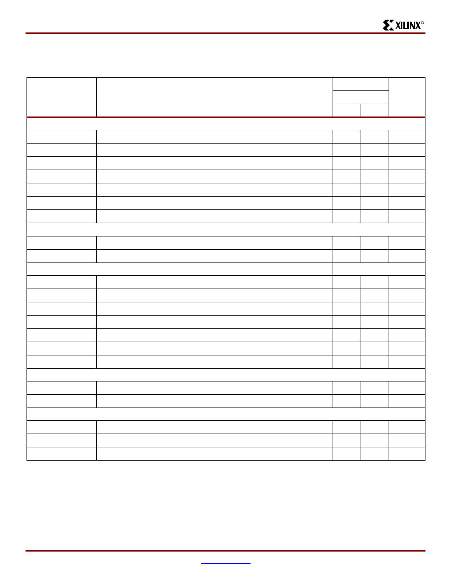
Features
∑
Certified to MIL-PRF-38535 (Qualified Manufacturer
Listing)
∑
Guaranteed over the full military temperature range
(≠55
∞
C to +125
∞
C)
∑
Ceramic and Plastic Packages
∑
Fast, high-density Field-Programmable Gate Arrays
-
Densities from 100K to 1M system gates
-
System performance up to 200 MHz
-
Hot-swappable for Compact PCI
∑
Multi-standard SelectI/OTM interfaces
-
16 high-performance interface standards
-
Connects directly to ZBTRAM devices
∑
Built-in clock-management circuitry
-
Four dedicated delay-locked loops (DLLs) for
advanced clock control
-
Four primary low-skew global clock distribution
nets, plus 24 secondary global nets
∑
Hierarchical memory system
-
LUTs configurable as 16-bit RAM, 32-bit RAM,
16-bit dual-ported RAM, or 16-bit Shift Register
-
Configurable synchronous dual-ported 4K-bit
RAMs
-
Fast interfaces to external high-performance RAMs
∑
Flexible architecture that balances speed and density
-
Dedicated carry logic for high-speed arithmetic
-
Dedicated multiplier support
-
Cascade chain for wide-input functions
-
Abundant registers/latches with clock enable, and
dual synchronous/asynchronous set and reset
-
Internal 3-state bussing
-
IEEE 1149.1 boundary-scan logic
-
Die-temperature sensing device
∑
Supported by FPGA FoundationTM and Alliance
Development Systems
-
Complete support for Unified Libraries, Relationally
Placed Macros, and Design Manager
-
Wide selection of PC and workstation platforms
∑
SRAM-based in-system configuration
-
Unlimited reprogrammability
-
Four programming modes
∑
0.22
µ
m 5-layer metal process
∑
100% factory tested
∑
Available to Standard Microcircuit Drawings
-
5962-99572 for XQV300
-
5962-99573 for XQV600
-
5962-99574 for XQV1000
-
Contact Defense Supply Center Columbus (DSCC)
for more information at
http://www.dscc.dla.mil
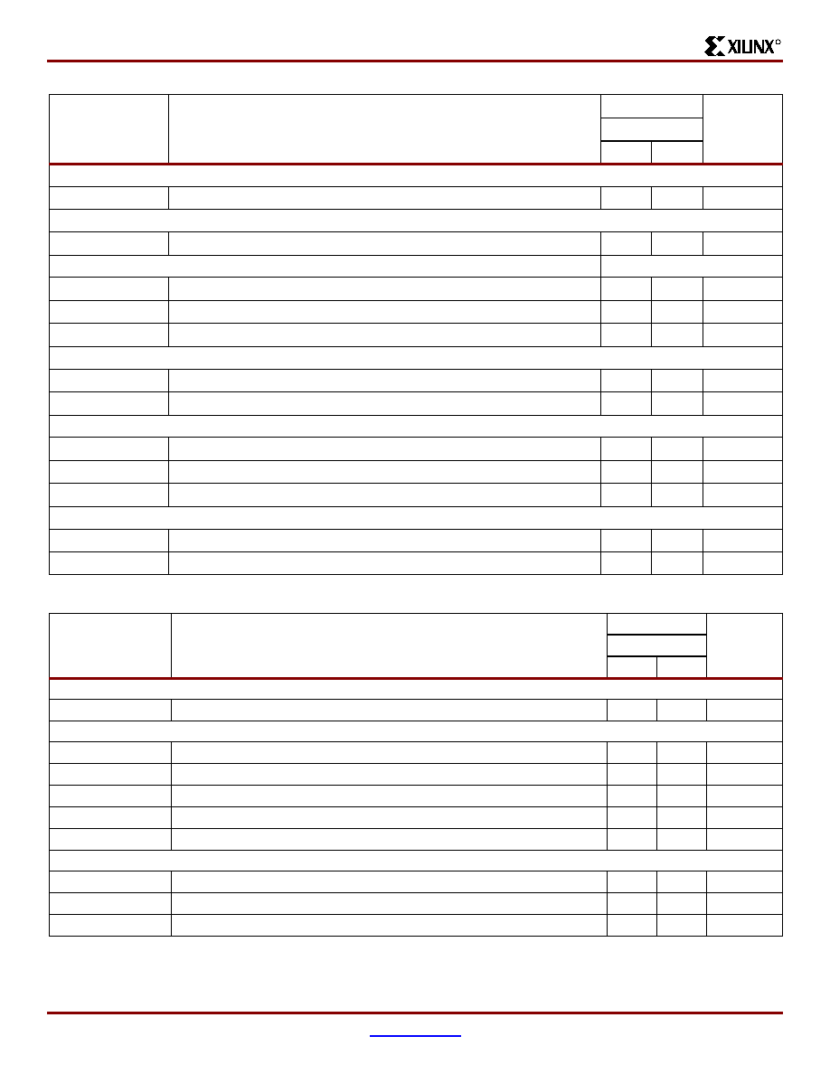
Description
The QProTM VirtexTM FPGA family delivers high-perfor-
mance, high-capacity programmable logic solutions. Dra-
matic increases in silicon efficiency result from optimizing
the new architecture for place-and-route efficiency and
exploiting an aggressive 5-layer-metal 0.22
µ
m CMOS pro-
cess. These advances make QPro Virtex FPGAs powerful
and flexible alternatives to mask-programmed gate arrays.
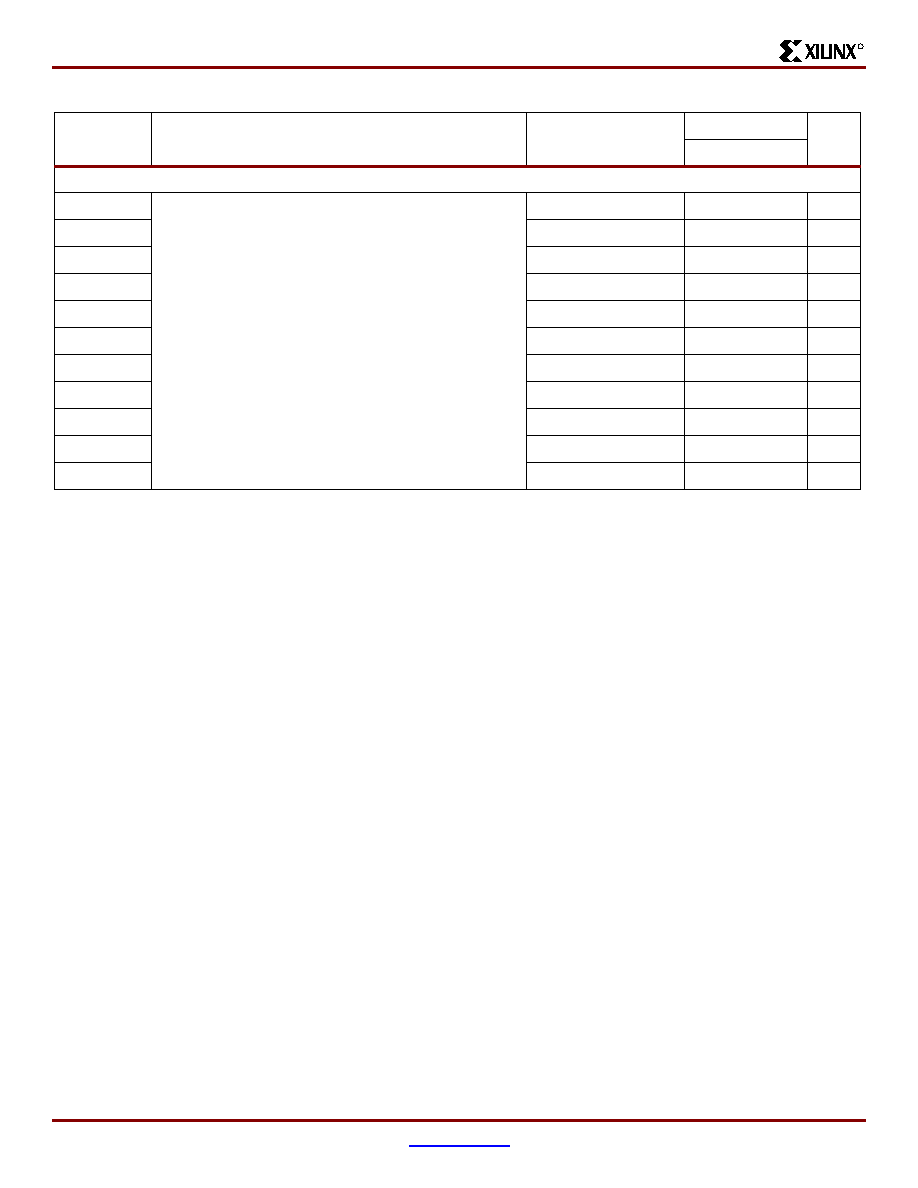
The Virtex family comprises the four members shown in
Table 1
.
Building on experience gained from previous generations of
FPGAs, the Virtex family represents a revolutionary step
forward in programmable logic design. Combining a wide
variety of programmable system features, a rich hierarchy of
fast, flexible interconnect resources, and advanced process
technology, the QPro Virtex family delivers a high-speed
and high-capacity programmable logic solution that
enhances design flexibility while reducing time-to-market.
Refer to the
"VirtexTM 2.5V Field Programmable Gate
Arrays"
commercial data sheet for more information on
device architecture and timing specifications.
0
QPro
Virtex 2.5V QML
High-Reliability FPGAs
DS002 (v1.5) December 5, 2001
0
2
Preliminary Product Specification
R

QPro Virtex 2.5V QML High-Reliability FPGAs
2
www.xilinx.com
DS002 (v1.5) December 5, 2001
1-800-255-7778
Preliminary Product Specification
R
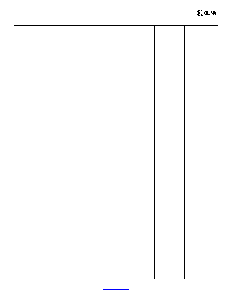
Virtex Electrical Characteristics
Based on preliminary characterization. Further changes are not expected.
All specifications are representative of worst-case supply voltage and junction temperature conditions. The parameters
included are common to popular designs and typical applications. Contact the factory for design considerations requiring
more detailed information.
Virtex DC Characteristics
Absolute Maximum Ratings
Table 1: QPro Virtex Field-Programmable Gate Array Family Members
Device
System Gates
CLB Array
Logic Cells
Maximum
Available I/O
Block RAM Bits
Max Select
RAM Bits
XQV100
108,904
20 x 30
2,700
180
40,960
38,400
XQV300
322,970
32 x 48
6,912
316
65,536
98,304
XQV600
661,111
48 x 72
15,552
316
98,304
221,184
XQV1000
1,124,022
64 x 96
27,648
404
131,072
393,216
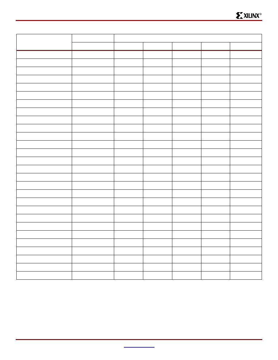
Symbol
Description Min/Max
Units
V
CCINT
Supply voltage relative to GND
≠0.5 to 3.0
V
V
CCO
Supply voltage relative to GND
≠0.5 to 4.0
V
V
REF
Input reference Voltage
≠0.5 to 3.6
V
V
IN
(3)
Input voltage relative to GND
Using V
REF
≠0.5 to 3.6
V
Internal threshold
≠0.5 to 5.5
V
V
TS
Voltage applied to 3-state output
≠0.5 to 5.5
V
V
CC
Longest supply voltage rise time from 1V to 2.375V
50
ms
T
STG
Storage temperature (ambient)
≠65 to +150
∞
C
T
J
Junction temperature
Ceramic packages
+150
∞
C
Plastic packages
+125
∞
C
Notes:
1.
Stresses beyond those listed under Absolute Maximum Ratings may cause permanent damage to the device. These are stress
ratings only, and functional operation of the device at these or any other conditions beyond those listed under Operating Conditions
is not implied. Exposure to Absolute Maximum Ratings conditions for extended periods of time may affect device reliability.
2.
Power supplies may turn on in any order.
3.
For protracted periods (e.g., longer than a day), V
IN
should not exceed V
CCO
by more that 3.6V.
QPro Virtex 2.5V QML High-Reliability FPGAs
DS002 (v1.5) December 5, 2001
www.xilinx.com
3
Preliminary Product Specification
1-800-255-7778
R
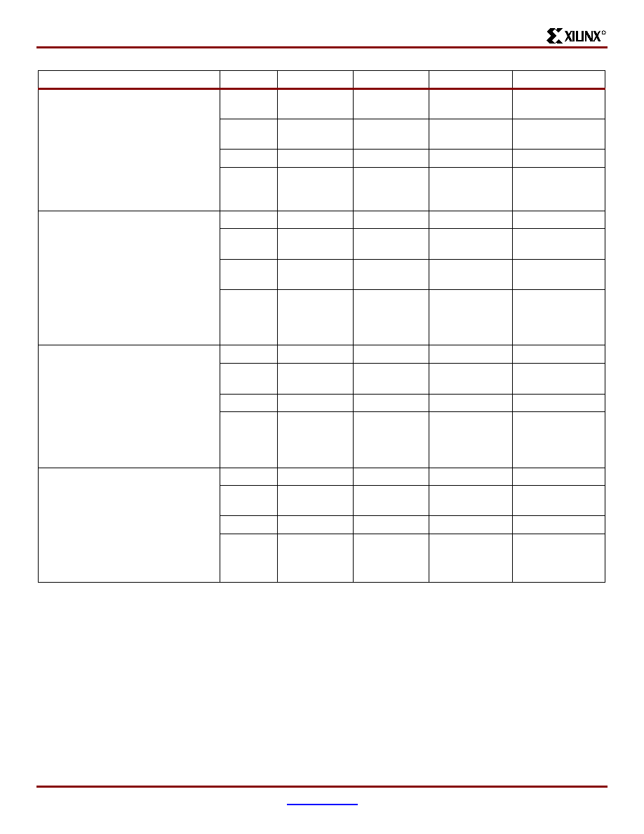
Recommended Operating Conditions
DC Characteristics Over Recommended Operating Conditions
Symbol
Description
Min
Max
Units
V
CCINT
Supply voltage relative to GND, T
C
= ≠55
∞
C to +125
∞
C
Ceramic packages
2.5 ≠ 5%
2.5 + 5%
V
Supply voltage relative to GND, T
J
= ≠55
∞
C to +125
∞
C
Plastic packages
2.5 ≠ 5%
2.5 + 5%
V
V
CCO
Supply voltage relative to GND, T
C
= ≠55
∞
C to +125
∞
C
Ceramic packages
1.2
3.6
V
Supply voltage relative to GND, T
J
= ≠55
∞
C to +125
∞
C
Plastic packages
1.2
3.6
V
T
IN
Input signal transition time
-
250
ns
T
IC
Initialization Temperature Range
(4)
XQVR300
≠55
+125
∞
C
XQVR600
≠55
+125
∞
C
XQVR1000
≠40
+125
∞
C
T
OC
Operational Temperature Range
(5)
XQVR300
≠55
+125
∞
C
XQVR600
≠55
+125
∞
C
XQVR1000
≠55
+125
∞
C
Notes:
1.
Correct operation is guaranteed with a minimum V
CCINT
of 2.25V (Nominal V
CCINT
≠ 10%). Below the minimum value stated above,
all delay parameters increase by 3% for each 50 mV reduction in V
CCINT
below the specified range.
2.
At junction temperatures above those listed as Operating Conditions, all delay parameters increase by 0.35% per
∞
C.
3.
Input and output measurement threshold is ~50% of V
CC
.
4.
Initialization occurs from the moment of V
CC
ramp-up to the rising transition of the INIT pin.
5.
The device is operational after the INIT pin has transitioned high.
Symbol
Description
Device
Min
Max
Units
V
DRINT
Data retention V
CCINT
voltage
(below which configuration data may be lost)
All
2.0
-
V
V
DRIO
Data retention V
CCO
voltage
(below which configuration data may be lost)
All
1.2
-
V
I
CCINTQ
Quiescent V
CCINT
supply current
(1)
XQV100
-
50
mA
XQV300
-
75
mA
XQV600
-
100
mA
XQV1000
-
100
mA
I
CCOQ
Quiescent V
CCINT
supply current
(1)
XQV100
-
2
mA
XQV300
-
2
mA
XQV600
-
2
mA
XQV1000
-
2
mA
I
REF
V
REF
current per V
REF
pin
-
-
20
µ
A
I
L
Input or output leakage current
-
≠10
+10
µ
A
C
IN
Input capacitance (sample tested)
-
-
8
pF
I
RPU
Pad pull-up (when selected) at V
IN
= 0V, V
CCO
= 3.3V (sample tested)
-
(2)
0.25
mA
I
RPD
Pad pull-down (when selected) at V
IN
= 3.6V (sample tested)
-
(2)
0.15
mA
Notes:
1.
With no output current loads, no active input pull-up resistors, all I/O pins in a High-Z state and floating.
2.
Internal pull-up and pull-down resistors guarantee valid logic levels at unconnected input pins. These pull-up and pull-down resistors
do not guarantee valid logic levels when input pins are connected to other circuits.
QPro Virtex 2.5V QML High-Reliability FPGAs
4
www.xilinx.com
DS002 (v1.5) December 5, 2001
1-800-255-7778
Preliminary Product Specification
R
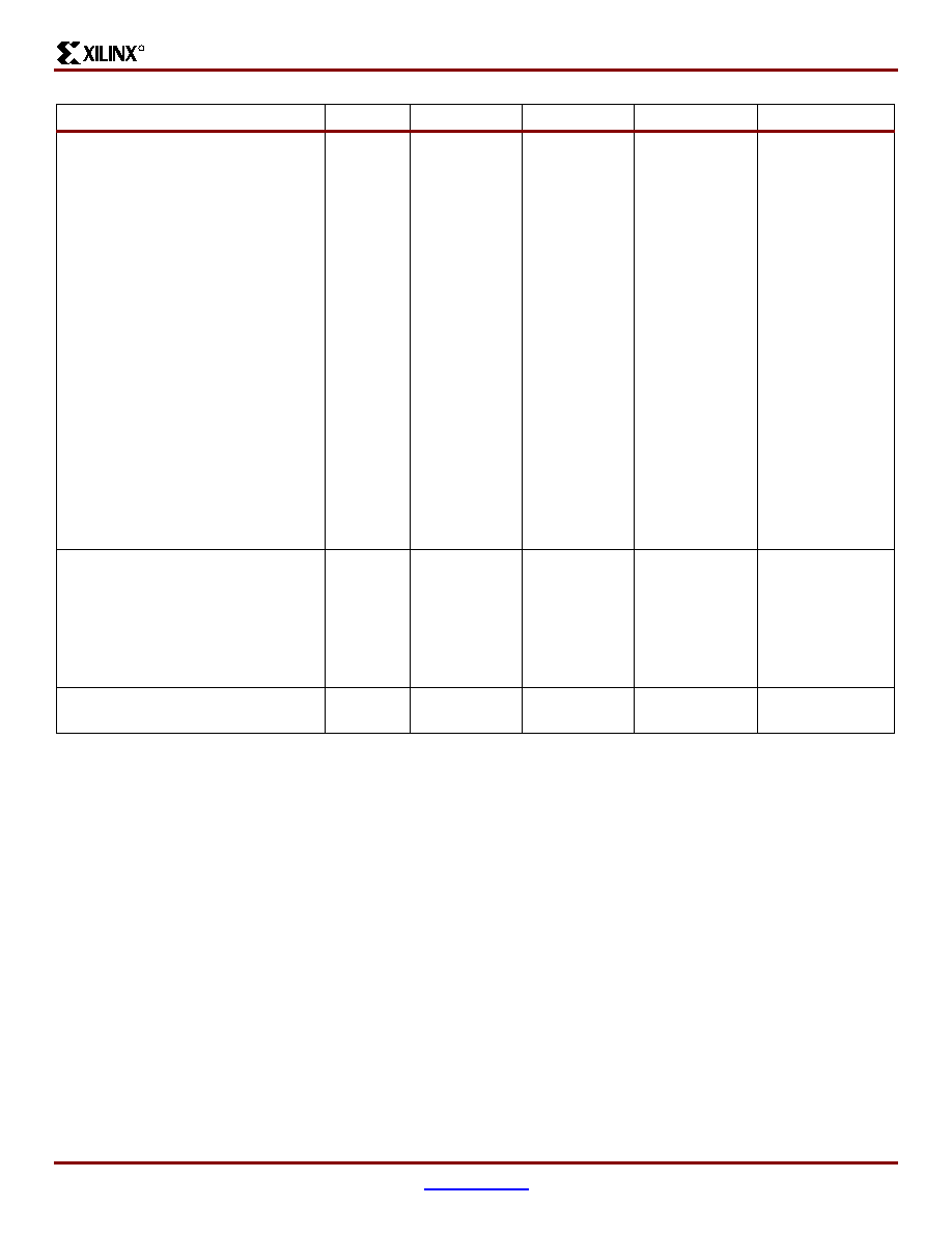
DC Input and Output Levels
Values for V
IL
and V
IH
are recommended input voltages.
Values for I
OL
and I
OH
are guaranteed output currents over
the recommended operating conditions at the V
OL
and V
OH
test points. Only selected standards are tested. These are
chosen to ensure that all standards meet their specifica-
tions. The selected standards are tested at minimum V
CCO
with the respective V
OL
and V
OH
voltage levels shown.
Other standards are sample tested.
Input/Output
Standard
V
IL
V
IH
V
OL
V
OH
I
OL
I
OH
V, min
V, max
V, min
V, max
V, max
V, min
mA
mA
LVTTL
(1)
≠0.5
0.8
2.0
5.5
0.4
2.4
24
≠24
LVCMOS2
≠0.5
0.7
1.7
5.5
0.4
1.9
12
≠12
PCI, 3.3V
≠0.5
44% V
CCINT
60% V
CCINT
V
CCO
+ 0.5
10% V
CCO
90% V
CCO
(2)
(2)
PCI, 5.0V
≠0.5
0.8
2.0
5.5
0.55
2.4
(2)
(2)
GTL
≠0.5
V
REF
≠ 0.05
V
REF
+ 0.05
3.6
0.4
n/a
40
n/a
GTL+
≠0.5
V
REF
≠ 0.1
V
REF
+ 0.1
3.6
0.6
n/a
36
n/a
HSTL I
≠0.5
V
REF
≠ 0.1
V
REF
+ 0.1
3.6
0.4
V
CCO
≠ 0.4
8
-8
HSTL III
≠0.5
V
REF
≠ 0.1
V
REF
+ 0.1
3.6
0.4
V
CCO
≠ 0.4
24
≠8
HSTL IV
≠0.5
V
REF
≠ 0.1
V
REF
+ 0.1
3.6
0.4
V
CCO
≠ 0.4
48
≠8
SSTL3 I
≠0.5
V
REF
≠ 0.2
V
REF
+ 0.2
3.6
V
REF
≠ 0.6
V
REF
+ 0.6
8
≠8
SSTL3 II
≠0.5
V
REF
≠ 0.2
V
REF
+ 0.2
3.6
V
REF
≠ 0.8
V
REF
+ 0.8
16
≠16
SSTL2 I
≠0.5
V
REF
≠ 0.2
V
REF
+ 0.2
3.6
V
REF
≠ 0.65
V
REF
+ 0.65
7.6
≠7.6
SSTL2 II
≠0.5
V
REF
≠ 0.2
V
REF
+ 0.2
3.6
V
REF
≠ 0.80
V
REF
+ 0.80
15.2
≠15.2
CTT
≠0.5
V
REF
≠ 0.2
V
REF
+ 0.2
3.6
V
REF
≠ 0.4
V
REF
+ 0.4
8
≠8
AGP
≠0.5
V
REF
≠ 0.2
V
REF
+ 0.2
3.6
10% V
CCO
90% V
CCO
(2)
(2)
Notes:
1.
V
OL
and V
OH
for lower drive currents are sample tested.
2.
Tested according to the relevant specifications.
QPro Virtex 2.5V QML High-Reliability FPGAs
DS002 (v1.5) December 5, 2001
www.xilinx.com
5
Preliminary Product Specification
1-800-255-7778
R
Virtex Switching Characteristics
Testing of switching parameters is modeled after testing
methods specified by MIL-M-38510/605. All devices are
100% functionally tested. Internal timing parameters are
derived from measuring internal test patterns. Listed below
are representative values. For more specific, more precise,
and worst-case guaranteed data, use the values reported
by the static timing analyzer (TRCE in the Xilinx Develop-
ment System) and back-annotated to the simulation netlist.
All timing parameters assume worst-case operating condi-
tions (supply voltage and junction temperature). Values
apply to all Virtex devices unless otherwise noted.
IOB Input Switching Characteristics
Input delays associated with the pad are specified for
LVTTL levels. For other standards, adjust the delays with
the values shown in
"IOB Input Switching Characteristics
Standard Adjustments" on page 6
.
Symbol
Description
Device
Speed Grade
Units
-4
Min
Max
Propagation Delays
T
IOPI
Pad to I output, no delay
All
-
1.0
ns
T
IOPID
Pad to I output, with delay
XQV100
-
1.9
ns
XQV300
-
1.9
ns
XQV600
-
2.3
ns
XQV1000
-
2.7
ns
T
IOPLI
Pad to output IQ via transparent latch, no
delay
All
-
2.0
ns
T
IOPLID
Pad to output IQ via transparent latch, with
delay
XQV100
-
4.8
ns
XQV300
-
5.1
ns
XQV600
-
5.5
ns
XQV1000
-
5.9
ns
Sequential Delays
T
IOCKIQ
Clock CLK to output IQ
All
-
0.8
ns
Setup and Hold Times with Respect to Clock CLK
Setup Time / Hold Time
T
IOPICK
/ T
IOICKP
Pad, no delay
All
2.0 / 0
-
ns
T
IOPICKD
/ T
IOICKPD
Pad, with delay
All
5.0 / 0
-
ns
T
IOICECK
/ T
IOCKICE
ICE input
All
1.0 / 0
-
ns
T
IOSRCKI
/ T
IOCKISR
SR input (IFF, synchronous)
All
1.3 / 0
-
ns
Set/Reset Delays
T
IOSRIQ
SR input to IQ (asynchronous)
All
-
1.8
ns
T
GSRQ
GSR to output IQ
All
-
12.5
ns
Notes:
1.
A Zero "0" Hold Time listing indicates no hold time or a negative hold time. Negative values can not be guaranteed "best-case",
but if a "0" is listed, there is no positive hold time.
QPro Virtex 2.5V QML High-Reliability FPGAs
6
www.xilinx.com
DS002 (v1.5) December 5, 2001
1-800-255-7778
Preliminary Product Specification
R
IOB Input Switching Characteristics Standard Adjustments
Symbol
Description
Standard
Speed Grade
Units
-4
Data Input Delay Adjustments
T
ILVTTL
Standard-specific data input delay adjustments
LVTTL
0.0
ns
T
ILVCMOS2
LVCMOS2
≠0.05
ns
T
IPCI33_3
PCI, 33 MHz, 3.3V
≠0.14
ns
T
IPCI33_5
PCI, 33 MHz, 5.0V
0.33
ns
T
IGTL
GTL
0.26
ns
T
IGTLP
GTL+
0.14
ns
T
IHSTL
HSTL
0.04
ns
T
ISSTL2
SSTL2
≠0.10
ns
T
ISSTL3
SSTL3
≠0.06
ns
T
ICTT
CTT
0.02
ns
T
IAGP
AGP
≠0.08
ns
QPro Virtex 2.5V QML High-Reliability FPGAs
DS002 (v1.5) December 5, 2001
www.xilinx.com
7
Preliminary Product Specification
1-800-255-7778
R
IOB Output Switching Characteristics
Output delays terminating at a pad are specified for LVTTL with 12 mA drive and fast slew rate. For other standards, adjust
the delays with the values shown in
"IOB Output Switching Characteristics Standard Adjustments" on page 8
.
Symbol
Description
Speed Grade
Units
-4
Min
Max
Propagation Delays
T
IOOP
O input to pad
-
3.5
ns
T
IOOLP
O input to pad via transparent latch
-
4.0
ns
3-State Delays
T
IOTHZ
T input to pad high-impedance
(1)
-
2.4
ns
T
IOTON
T input to valid data on pad
-
3.7
ns
T
IOTLPHZ
T input to pad high-impedance via transparent latch
(1)
-
3.0
ns
T
IOTLPON
T input to valid data on pad via transparent latch
-
4.2
ns
T
GTS
GTS to pad high-impedance
(1)
-
6.3
ns
Sequential Delays
T
IOCKP
Clock CLK to pad
-
3.5
ns
T
IOCKHZ
Clock CLK to pad high-impedance (synchronous)
(1)
-
2.9
ns
T
IOCKON
Clock CLK to valid data on pad (synchronous)
-
4.1
ns
Setup and Hold Times before/after Clock CLK
Setup Time / Hold Time
(2)
T
IOOCK
/T
IOCKO
O input
1.3 / 0
-
ns
T
IOOCECK
/T
IOCKOCE
OCE input
1.0 / 0
-
ns
T
IOSRCKO
/T
IOCKOSR
SR input (OFF)
1.4 / 0
-
ns
T
IOTCK
/T
IOCKT
3-state setup times, T input
0.9 / 0
-
ns
T
IOTCECK
/T
IOCKTCE
3-state setup times, TCE input
1.1 / 0
-
ns
T
IOSRCKT
/T
IOCKTSR
3-state setup times, SR input (TFF)
1.3 / 0
-
ns
Set/Reset Delays
T
IOSRP
SR input to pad (asynchronous)
4.6
-
ns
T
IOSRHZ
SR input to pad high-impedance (asynchronous)
(1)
3.9
-
ns
T
IOSRON
SR input to valid data on pad (asynchronous)
5.1
-
ns
Notes:
1.
High-impedance turn-off delays should not be adjusted.
2.
A Zero "0" Hold Time listing indicates no hold time or a negative hold time. Negative values can not be guaranteed "best-case", but
if a "0" is listed, there is no positive hold time.
QPro Virtex 2.5V QML High-Reliability FPGAs
8
www.xilinx.com
DS002 (v1.5) December 5, 2001
1-800-255-7778
Preliminary Product Specification
R
IOB Output Switching Characteristics Standard Adjustments
Output delays terminating at a pad are specified for LVTTL with 12 mA drive and fast slew rate. For other standards, adjust
the delays by the values shown.
Symbol
Description
Standard
Speed Grade
Units
-4
Output Delay Adjustments
T
OLVTTL_S2
Standard-specific adjustments for output delays
terminating at pads (based on standard capacitive
load, C
sl
)
LVTTL, slow
2 mA
17.0
ns
T
OLVTTL_S4
4 mA
8.6
ns
T
OLVTTL_S6
6 mA
5.6
ns
T
OLVTTL_S8
8 mA
3.5
ns
T
OLVTTL_S12
12 mA
2.2
ns
T
OLVTTL_S16
16 mA
2.0
ns
T
OLVTTL_S24
24 mA
1.6
ns
T
OLVTTL_F2
LVTTL, fast
2 mA
15.1
ns
T
OLVTTL_F4
4 mA
6.1
ns
T
OLVTTL_F6
6 mA
3.6
ns
T
OLVTTL_F8
8 mA
1.2
ns
T
OLVTTL_F12
12 mA
0.0
ns
T
OLVTTL_F16
16 mA
≠0.05
ns
T
OLVTTL_F24
24 mA
≠0.23
ns
T
OLVCMOS2
LVCMOS2
0.12
ns
T
OPCI33_3
PCI, 33 MHz, 3.3V
2.7
ns
T
OPCI33_5
PCI, 33 MHz, 5.0V
3.3
ns
T
OGTL
GTL
0.6
ns
T
OGTLP
GTL+
1.0
ns
T
OHSTL_I
HSTL I
≠0.5
ns
T
OHSTL_III
HSTL III
≠1.0
ns
T
OHSTL_IV
HSTL IV
≠1.1
ns
T
OSSTL2_I
SSTL2 I
≠0.5
ns
T
OSSTL2_II
SSTL2 II
≠1.0
ns
T
OSSTL3_I
SSTL3 I
≠0.5
ns
T
OSSTL3_II
SSTL3 II
≠1.1
ns
T
OCTT
CTT
≠0.6
ns
T
OAGP
AGP
≠1.0
ns
QPro Virtex 2.5V QML High-Reliability FPGAs
DS002 (v1.5) December 5, 2001
www.xilinx.com
9
Preliminary Product Specification
1-800-255-7778
R
Calculation of T
ioop
as a Function of Capacitance
The values for T
ioop
were based on the standard capacitive
load (Csl) for each I/O standard as listed in
Table 2
.
For other capacitive loads, use the formulas below to calcu-
late the corresponding T
ioop
:
T
ioop
= T
ioopl
+ T
opadjust
+
(C
load
- C
sl
) * fl
Where:
T
opadjust
is reported above in the Output Delay
Adjustment section.
C
load
is the capacitive load for the design.
Clock Distribution Guidelines and Switching Characteristics
Table 2: Constants for Use in Calculation of T
op
Standard
C
sl
(pF)
fl (ns/pF)
LVTTL slow
slew rate
2 mA drive
35
0.41
4 mA drive
35
0.20
6 mA drive
35
0.100
8 mA drive
35
0.086
12 mA drive
35
0.058
16 mA drive
35
0.050
24 mA drive
35
0.048
LVTTL fast
slew rate
2 mA drive
35
0.41
4 mA drive
35
0.20
6 mA drive
35
0.13
8 mA drive
35
0.079
12 mA drive
35
0.044
16 mA drive
35
0.043
24 mA drive
35
0.033
LVCMOS2
35
0.041
PCI 33 MHz 5V
50
0.050
PCI 33 MHZ 3.3V
10
0.050
GTL
0
0.014
GTL+
0
0.017
HSTL Class I
20
0.022
HSTL Class III
20
0.016
HSTL Class IV
20
0.014
SSTL2 Class I
30
0.028
SSTL2 Class II
30
0.016
SSTL3 Class 1
30
0.029
SSTL3 Class II
30
0.016
CTT
20
0.035
AGP
10
0.037
Table 2: Constants for Use in Calculation of T
op
Standard
C
sl
(pF)
fl (ns/pF)
Symbol
Description
Device
Speed Grade
Units
-4
Min
Max
Global Clock Skew
T
GSKEWIOB
Global clock skew between IOB flip-flops
XQV100
-
0.15
ns
XQV300
-
0.18
ns
XQV600
-
0.17
ns
XQV1000
-
0.25
ns
T
GPIO
Global clock PAD to output
All
-
0.9
ns
T
GIO
Global clock buffer I input to O output
All
-
0.9
ns
Notes:
1.
These clock-distribution delays are provided for guidance only. They reflect the delays encountered in a typical design under
worst-case conditions. Precise values for a particular design are provided by the timing analyzer.
QPro Virtex 2.5V QML High-Reliability FPGAs
10
www.xilinx.com
DS002 (v1.5) December 5, 2001
1-800-255-7778
Preliminary Product Specification
R
CLB Switching Characteristics
Delays originating at F/G inputs vary slightly according to the input used. The values listed below are worst-case. Precise
values are provided by the timing analyzer.
Symbol
Description
Speed Grade
Units
-4
Min
Max
Combinatorial Delays
T
ILO
4-input function: F/G inputs to X/Y outputs
-
0.8
ns
T
IF5
5-input function: F/G inputs to F5 output
-
0.9
ns
T
IF5X
5-input function: F/G inputs to X output
-
1.0
ns
T
IF6Y
6-input function: F/G inputs to Y output via F6 MUX
-
1.2
ns
T
F5INY
6-input function: F5IN input to Y output
-
0.5
ns
T
IFNCTL
Incremental delay routing through transparent latch to XQ/YQ outputs
-
0.8
ns
T
BYYB
BY input to YB output
-
0.7
ns
Sequential Delays
T
CKO
FF clock CLK to XQ/YQ outputs
-
1.4
ns
T
CKLO
Latch clock CLK to XQ/YQ outputs
-
1.6
ns
Setup and Hold Times before/after Clock CLK
Setup Time / Hold Time
T
ICK
/T
CKI
4-input function: F/G Inputs
1.5 / 0
-
ns
T
IF5CK
/T
CKIF5
5-input function: F/G inputs
1.7 / 0
-
ns
T
F5INCK
/T
CKF5IN
6-input function: F5IN input
1.2 / 0
-
ns
T
IF6CK
/T
CKIF6
6-input function: F/G inputs via F6 MUX
1.9 / 0
-
ns
T
DICK
/T
CKDI
BX/BY inputs
0.8 / 0
-
ns
T
CECK
/T
CKCE
CE input
1.0 / 0
-
ns
T
RCK
T
CKR
SR/BY inputs (synchronous)
0.9 / 0
-
ns
Clock CLK
T
CH
Minimum pulse width, High
2.0
-
ns
T
CL
Minimum pulse width, Low
2.0
-
ns
Set/Reset
T
RPW
Minimum pulse width, SR/BY inputs
3.3
-
ns
T
RQ
Delay from SR/BY inputs to XQ/YQ outputs (asynchronous)
-
1.4
ns
T
IOGSRQ
Delay from GSR to XQ/YQ outputs
-
12.5
ns
Notes:
1.
A Zero "0" Hold Time listing indicates no hold time or a negative hold time. Negative values can not be guaranteed "best-case", but
if a "0" is listed, there is no positive hold time.

QPro Virtex 2.5V QML High-Reliability FPGAs
DS002 (v1.5) December 5, 2001
www.xilinx.com
11
Preliminary Product Specification
1-800-255-7778
R
CLB Arithmetic Switching Characteristics
Setup times not listed explicitly can be approximated by decreasing the combinatorial delays by the setup time adjustment
listed. Precise values are provided by the timing analyzer.
Symbol
Description
Speed Grade
Units
-4
Min
Max
Combinatorial Delays
T
OPX
F operand inputs to X via XOR
-
1.0
ns
T
OPXB
F operand input to XB output
-
1.4
ns
T
OPY
F operand input to Y via XOR
-
2.0
ns
T
OPYB
F operand input to YB output
-
2.0
ns
T
OPCYF
F operand input to COUT output
-
1.5
ns
T
OPGY
G operand inputs to Y via XOR
-
1.2
ns
T
OPGYB
G operand input to YB output
-
2.1
ns
T
OPCYG
G operand input to COUT output
-
1.6
ns
T
BXCY
BX initialization input to COUT
-
1.1
ns
T
CINX
CIN input to X output via XOR
-
0.6
ns
T
CINXB
CIN input to XB
-
0.1
ns
T
CINY
CIN input to Y via XOR
-
0.6
ns
T
CINYB
CIN input to YB
-
0.6
ns
T
BYP
CIN input to COUT output
-
0.2
ns
Multiplier Operation
T
FANDXB
F1/2 operand inputs to XB output via AND
-
0.5
ns
T
FANDYB
F1/2 operand inputs to YB output via AND
-
1.1
ns
T
FANDCY
F1/2 operand inputs to COUT output via AND
-
0.6
ns
T
GANDYB
G1/2 operand inputs to YB output via AND
-
0.7
ns
T
GANDCY
G1/2 operand inputs to COUT output via AND
-
0.2
ns
Setup and Hold Times before/after Clock CLK
Setup Time / Hold Time
T
CCKX
/T
CKCX
CIN input to FFX
1.3 / 0
-
ns
T
CCKY
/T
CKCY
CIN input to FFY
1.4 / 0
-
ns
Notes:
1.
A Zero "0" Hold Time listing indicates no hold time or a negative hold time. Negative values can not be guaranteed "best-case", but if
a "0" is listed, there is no positive hold time.
QPro Virtex 2.5V QML High-Reliability FPGAs
12
www.xilinx.com
DS002 (v1.5) December 5, 2001
1-800-255-7778
Preliminary Product Specification
R
CLB SelectRAM Switching Characteristics
BLOCKRAM Switching Characteristics
Symbol
Description
Speed Grade
Units
-4
Min
Max
Sequential Delays
T
SHCKO
Clock CLK to X/Y outputs (WE active)
-
3.0
ns
Shift-Register Mode
T
SHCKO
Clock CLK to X/Y outputs
-
3.0
ns
Setup Times before Clock CLK
Setup Time / Hold Time
T
AS
/T
AH
F/G address inputs
0.7 / 0
-
ns
T
DS
/T
DH
BX/BY data inputs (DIN)
0.9 / 0
-
ns
T
WS
/T
WH
CE input (WE)
1.0 / 0
-
ns
Shift-Register Mode
T
SHDICK
BX/BY data inputs (DIN)
0.9
-
ns
T
SHCECK
CE input (WS)
1.0
-
ns
Clock CLK
T
WPH
Minimum pulse width, High
3.1
-
ns
T
WPL
Minimum pulse width, Low
3.1
-
ns
T
WC
Minimum clock period to meet address write cycle time
6.2
-
ns
Shift-Register Mode
T
SRPH
Minimum pulse width, High
3.1
-
ns
T
SRPL
Minimum pulse width, Low
3.1
-
ns
Symbol
Description
Speed Grade
Units
-4
Min
Max
Sequential Delays
T
BCKO
Clock CLK to DOUT output
-
4.1
ns
Setup Times Before Clock Clk
T
BACK
/T
BCKA
ADDR inputs
1.5 / 0
-
ns
T
BDCK
/T
BCKD
DIN inputs
1.5 / 0
-
ns
T
BECK
/T
BCKE
EN input
3.4 / 0
-
ns
T
BRCK
/T
BCKR
RST input
3.2 / 0
-
ns
T
BWCK
/T
BCKW
WEN input
3.0 / 0
-
ns
Clock CLK
T
BPWH
Minimum pulse width, High
2.0
-
ns
T
BPWL
Minimum pulse width, Low
2.0
-
ns
T
BCCS
CLKA -> CLKB setup time for different ports
4.0
-
ns
Notes:
1.
A Zero "0" Hold Time listing indicates no hold time or a negative hold time. Negative values can not be guaranteed "best-case", but
if a "0" is listed, there is no positive hold time.

QPro Virtex 2.5V QML High-Reliability FPGAs
DS002 (v1.5) December 5, 2001
www.xilinx.com
13
Preliminary Product Specification
1-800-255-7778
R
TBUF Switching Characteristics
JTAG Test Access Port Switching Characteristics
Virtex Pin-to-Pin Output Parameter Guidelines
Testing of switching parameters is modeled after testing
methods specified by MIL-M-38510/605. All devices are
100% functionally tested. Listed below are representative
values for typical pin locations and normal clock loading.
Values are expressed in nanoseconds unless otherwise
noted.
Global Clock Input to Output Delay for LVTTL, 12 mA, Fast Slew Rate, with DLL
Global Clock Input to Output Delay for LVTTL, 12 mA, Fast Slew Rate, without DLL
Symbol
Description
Speed Grade
Units
-4
Min
Max
Combinatorial Delays
T
IO
IN input to OUT output
-
0.0
ns
T
OFF
TRI input to OUT output high-impedance
-
0.2
ns
T
ON
Tri input to valid data on OUT output
-
0.2
ns
Symbol
Description
Speed Grade
Units
-4
Min
Max
T
TAPTCK
TMS and TDI setup times before TCK
4.0
-
ns
T
TCKTAP
TMS and TDI hold times after TCK
2.0
-
ns
T
TCKTDO
Output delay from clock TCK to output TDO
-
11.0
ns
F
TCK
Maximum TCK clock frequency
-
33
MHz
Symbol
Description
Device
Speed Grade
Units
-4
Min
Max
LVTTL Global Clock Input to Output Delay using Output Flip-flop,
12 mA, Fast Slew Rate, with DLL. For data output with different
standards, adjust the delays with the values shown in
"IOB Output
Switching Characteristics Standard Adjustments" on page 8
.
XQV100
-
3.6
ns
XQV300
-
3.6
ns
XQV600
-
3.6
ns
XQV1000
-
3.6
ns
Notes:
1.
Listed above are representative values where one global clock input drives one vertical clock line in each accessible column, and
where all accessible IOB and CLB flip-flops are clocked by the global clock net.
2.
Output timing is measured at 50% V
CC
threshold with 35 pF external capacitive load. For different loads, see
Table 2
.
3.
DLL output jitter is already included in the timing calculation.
Symbol
Description
Device
Speed Grade
Units
-4
Min
Max
LVTTL Global Clock Input to Output Delay using Output Flip-flop,
12 mA, Fast Slew Rate, without DLL. For data output with different
standards, adjust the delays with the values shown in
"IOB Output
Switching Characteristics Standard Adjustments" on page 8
.
XQV100
-
5.7
ns
XQV300
-
5.9
ns
XQV600
-
6.0
ns
XQV1000
-
6.3
ns
Notes:
1.
Listed above are representative values where one global clock input drives one vertical clock line in each accessible column,and
where all accessible IOB and CLB flip-flops are clocked by the global clock net.
2.
Output timing is measured at 50% V
CC
threshold with 35 pF external capacitive load. For different loads, see
Table 2
.
QPro Virtex 2.5V QML High-Reliability FPGAs
14
www.xilinx.com
DS002 (v1.5) December 5, 2001
1-800-255-7778
Preliminary Product Specification
R
Minimum Clock to Out for Virtex Devices
I/O Standard
With DLL
Without DLL
All Devices
V100
V300
V600
V1000
Units
LVTTL_S2
(1)
5.2
6.0
6.1
6.1
6.1
ns
LVTTL_S4
(1)
3.5
4.3
4.4
4.4
4.4
ns
LVTTL_S6
(1)
2.8
3.6
3.7
3.7
3.7
ns
LVTTL_S8
(1)
2.2
3.1
3.1
3.2
3.2
ns
LVTTL_S12
(1)
2.0
2.9
2.9
3.0
3.0
ns
LVTTL_S16
(1)
1.9
2.8
2.8
2.9
2.9
ns
LVTTL_S24
(1)
1.8
2.6
2.7
2.7
2.8
ns
LVTTL_F2
(1)
2.9
3.8
3.8
3.9
3.9
ns
LVTTL_F4
(1)
1.7
2.6
2.6
2.7
2.7
ns
LVTTL_F6
(1)
1.2
2.0
2.1
2.1
2.2
ns
LVTTL_F8
(1)
1.1
1.9
2.0
2.0
2.0
ns
LVTTL_F12
(1)
1.0
1.8
1.9
1.9
1.9
ns
LVTTL_F16
(1)
0.9
1.8
1.8
1.8
1.9
ns
LVTTL_F24
(1)
0.9
1.7
1.8
1.8
1.9
ns
LVCMOS2
1.1
1.9
2.0
2.0
2.1
ns
PCI33_3
1.5
2.4
2.4
2.5
2.5
ns
PCI33_5
1.4
2.2
2.3
2.3
2.4
ns
GTL
1.6
2.5
2.5
2.6
2.6
ns
GTL+
1.7
2.5
2.6
2.6
2.7
ns
HSTL I
1.1
1.9
2.0
2.0
2.0
ns
HSTL III
0.9
1.7
1.8
1.8
1.9
ns
HSTL IV
0.8
1.6
1.7
1.7
1.8
ns
SSTL2 I
0.9
1.7
1.8
1.8
1.8
ns
SSTL2 II
0.8
1.6
1.7
1.7
1.7
ns
SSTL3 I
0.8
1.7
1.7
1.7
1.8
ns
SSTL3 II
0.7
1.5
1.6
1.6
1.7
ns
CTT
1.0
1.8
1.9
1.9
2.0
ns
AGP
1.0
1.8
1.9
1.9
2.0
ns
Notes:
1.
S = Slow Slew Rate, F = Fast Slew Rate
2.
Listed above are representative values where one global clock input drives one vertical clock line in each accessible column. and
where all accessible IOB and CLB flip-flops are clocked by the global clock net.
3.
Output timing is measured at 50% V
CC
threshold with 8 pF external capacitive load.
QPro Virtex 2.5V QML High-Reliability FPGAs
DS002 (v1.5) December 5, 2001
www.xilinx.com
15
Preliminary Product Specification
1-800-255-7778
R
Virtex Pin-to-Pin Input Parameter Guidelines
Testing of switching parameters is modeled after testing
methods specified by MIL-M-38510/605. All devices are
100% functionally tested. Listed below are representative
values for typical pin locations and normal clock loading.
Values are expressed in nanoseconds unless otherwise
noted
Global Clock Setup and Hold for LVTTL Standard, with DLL
Global Clock Setup and Hold for LVTTL Standard, without DLL
Symbol
Description
Device
Speed Grade
Units
-4
Min
Max
Input Setup and Hold Time Relative to Global Clock Input Signal for LVTTL Standard. For data input with different
standards, adjust the setup time delay by the values shown in Input Delay Adjustments.
T
PSDLL
/T
PHDLL
No Delay
Global clock and IFF, with DLL
XQV100
2.1 / ≠0.4
-
ns
XQV300
2.1 / ≠0.4
-
ns
XQV600
2.1 / ≠0.4
-
ns
XQV1000
2.1 / ≠0.4
-
ns
Notes:
1.
IFF = Input Flip-Flop or Latch
2.
Setup time is measured relative to the Global Clock input signal with the fastest route and the lightest load. Hold time is measured
relative to the Global Clock input signal with the slowest route and heaviest load.
3.
DLL output jitter is already included in the timing calculation.
Symbol
Description
Device
Speed Grade
Units
-4
Min
Max
Input Setup and Hold Time Relative to Global Clock Input Signal for LVTTL Standard. For data input with different
standards, adjust the setup time delay by the values shown in Input Delay Adjustments.
T
PSFD
/T
PHFD
Full Delay
Global clock and IFF, without DLL
XQV100
3.0 / 0.0
-
ns
XQV300
3.1 / 0.0
-
ns
XQV600
3.3 / 0.0
-
ns
XQV1000
3.6 / 0.0
-
ns
Notes:
1.
IFF = Input Flip-Flop or Latch
2.
Setup time is measured relative to the Global Clock input signal with the fastest route and the lightest load. Hold time is measured
relative to the Global Clock input signal with the slowest route and heaviest load.
3.
A Zero "0" Hold Time listing indicates no hold time or a negative hold time. Negative values can not be guaranteed "best-case", but
if a "0" is listed, there is no positive hold time.
QPro Virtex 2.5V QML High-Reliability FPGAs
16
www.xilinx.com
DS002 (v1.5) December 5, 2001
1-800-255-7778
Preliminary Product Specification
R
DLL Timing Parameters
Switching parameters testing is modeled after testing meth-
ods specified by MIL-M-38510/605; all devices are 100 per-
cent functionally tested. Because of the difficulty in directly
measuring many internal timing parameters, those parame-
ters are derived from benchmark timing patterns. The fol-
lowing guidelines reflect worst-case values across the
recommended operating conditions.
Symbol
Description
Speed Grade -4
Units
Min
Max
F
CLKINHF
Input clock frequency (CLKDLLHF)
60
180
MHz
F
CLKINLF
Inputclock frequency (CLKDLL)
25
90
MHz
T
DLLPWHF
Input clock pulse width (CLKDLLHF)
2.4
-
ns
T
DLLPWLF
Input clock pulse width (CLKDLL)
3.0
-
ns
Notes:
1.
All specifications correspond to Commercial Operating Temperatures (0∞C to +100∞C).
Symbol
Description
CLKDLLHF
CLKDLL
Units
Min
Max
Min
Max
T
IPTOL
Input clock period tolerance
-
1.0
-
1.0
ns
T
IJITCC
Input clock jitter cycle to cycle
-
±
150
-
±
300
ps
T
LOCK
Time required for DLL to acquire Lock
F
CLKIN
> 60 MHz
-
20
-
20
µ
s
50-60 MHz
-
-
-
25
µ
s
40-50 MHz
-
-
-
50
µ
s
30-40 MHz
-
-
-
90
µ
s
25-30 MHz
-
-
-
120
µ
s
T
SKEW
DLL output skew (between any DLL output)
-
±
150
-
±
150
ps
T
OPHASE
DLL output long term phase differential
-
±
100
-
±
100
ps
T
OJITCC
DLL output ditter cycle to cycle
-
±
60
-
±
60
ps
Notes:
1.
All specifications correspond to Commercial Operating Temperatures (0∞C to +100∞C).
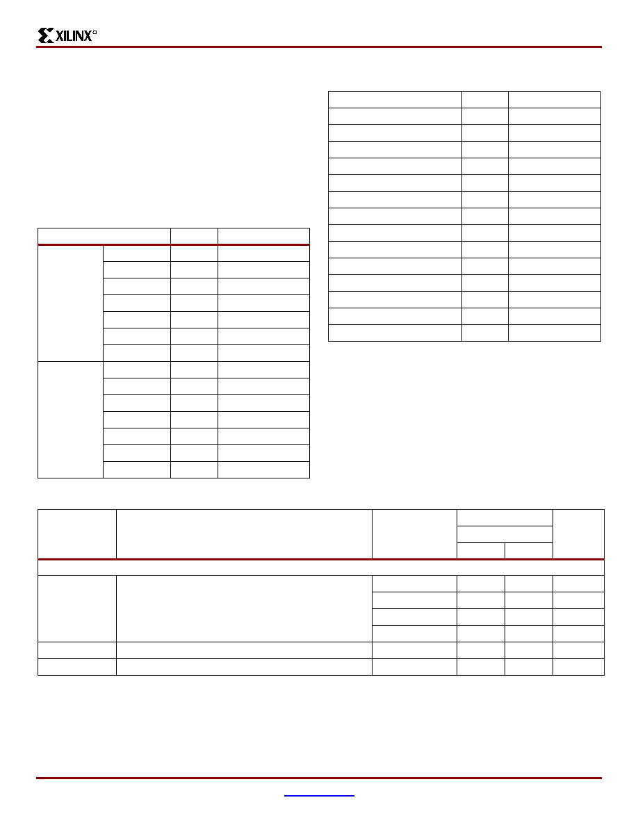
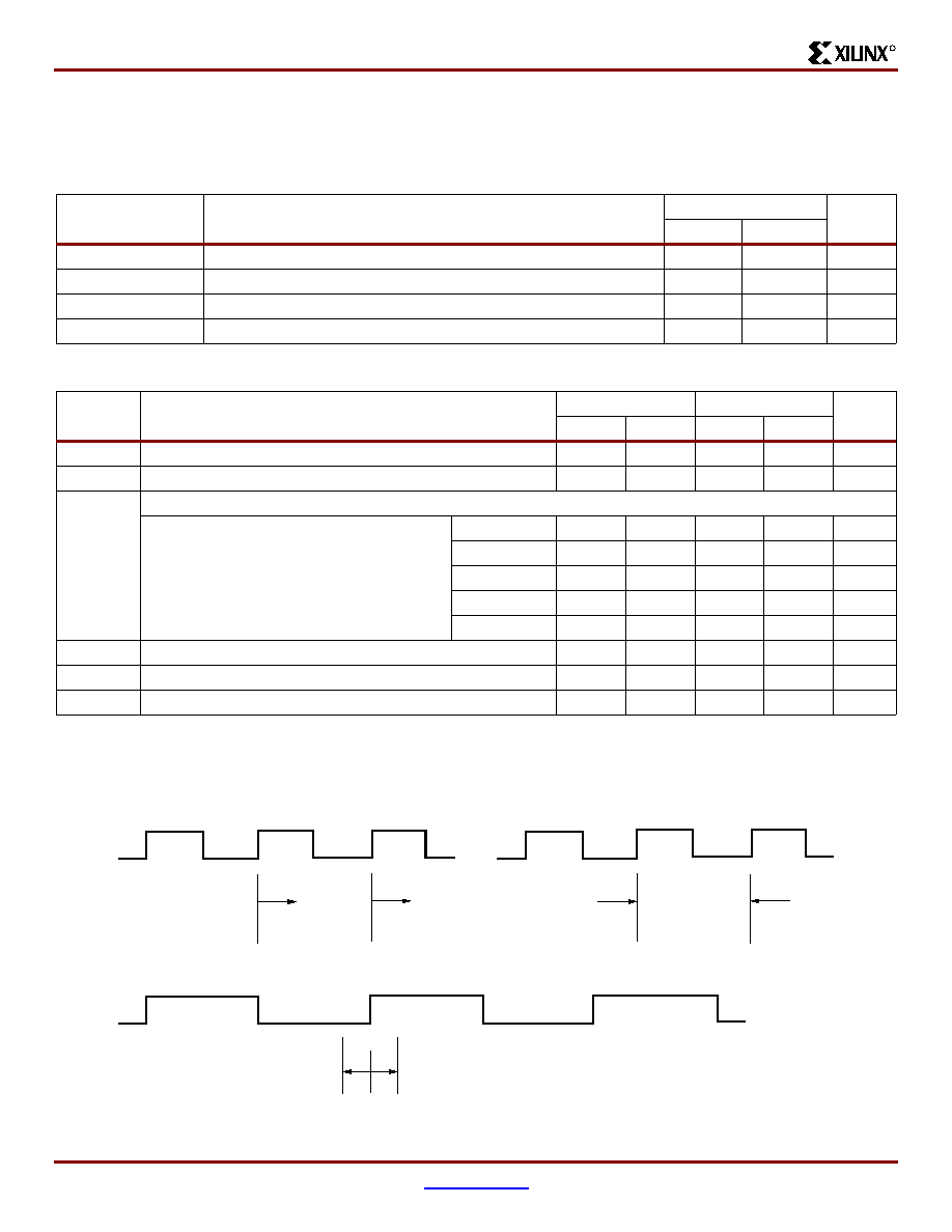
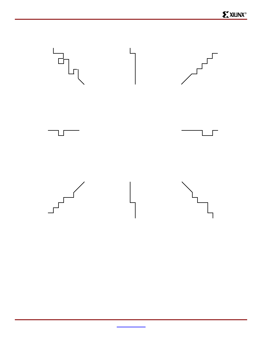
Figure 1: Frequency Tolerance and Clock Jitter
TCLKIN
TCLKIN + TIPTOL
Period Tolerance: the allowed input clock period change in nanoseconds.
Clock Jitter: the difference between an ideal reference clock edgfe and the actual design.
TOJITCC
+
_
_
DS002_01_060100
QPro Virtex 2.5V QML High-Reliability FPGAs
DS002 (v1.5) December 5, 2001
www.xilinx.com
17
Preliminary Product Specification
1-800-255-7778
R
QPro Virtex Pinouts
Pinout Tables
See the Xilinx WebLINX web site (
http://www.xil-
inx.com/partinfo/databook.htm
) for updates or additional
pinout information. For convenience,
Table 3
,
Table 4
and
Table 5
list the locations of special-purpose and power-sup-
ply pins. Pins not listed are user I/Os.
Table 3: Virtex QFP Package Pinout Information
Pin Name
Device
PQ/HQ240
GCK0
All
92
GCK1
All
89
GCK2
All
210
GCK3
All
213
M0
All
60
M1
All
58
M2
All
62
CCLK
All
179
PROGRAM
All
122
DONE
All
120
INIT
All
123
BUSY/DOUT
All
178
D0/DIN
All
177
D1
All
167
D2
All
163
D3
All
156
D4
All
145
D5
All
138
D6
All
134
D7
All
124
WRITE
All
185
CS
All
184
TDI
All
183
TDO
All
181
TMS
All
2
TCK
All
239
V
CCINT
All
16, 32, 43, 77, 88, 104,
137, 148, 164, 198, 214,
225
V
CCO
(The V
CCO
for the PQ/HQ240 package is common to all eight I/O
banks. Different output standards per I/O bank that require different
V
CCO
values cannot be supported.)
All
15, 30, 44, 61, 76, 90,
105, 121, 136, 150, 165,
180, 197, 212, 226, 240
QPro Virtex 2.5V QML High-Reliability FPGAs
18
www.xilinx.com
DS002 (v1.5) December 5, 2001
1-800-255-7778
Preliminary Product Specification
R
V
REF
, Bank 0
(V
REF
pins are listed incrementally. Connect all pins listed for both
the required device and all smaller devices listed in the same
package.)
Within each bank, if input reference voltage is not required, all V
REF
pins are general I/O.
XQV100
... + 229
XQV300
... + 236
XQV600
... + 230
V
REF
, Bank 1
(V
REF
pins are listed incrementally. Connect all pins listed for both
the required device and all smaller devices listed in the same
package.)
Within each bank, if input reference voltage is not required, all V
REF
pins are general I/O.
XQV100
... + 194
XQV300
... + 187
XQV600
... + 193
V
REF
, Bank 2
(V
REF
pins are listed incrementally. Connect all pins listed for both
the required device and all smaller devices listed in the same
package.)
Within each bank, if input reference voltage is not required, all V
REF
pins are general I/O.
XQV100
... + 168
XQV300
... + 175
XQV600
... + 169
V
REF
, Bank 3
(V
REF
pins are listed incrementally. Connect all pins listed for both
the required device and all smaller devices listed in the same
package.)
Within each bank, if input reference voltage is not required, all V
REF
pins are general I/O.
XQV100
... + 133
XQV300
... + 126
XQV600
... + 132
V
REF
, Bank 4
(V
REF
pins are listed incrementally. Connect all pins listed for both
the required device and all smaller devices listed in the same
package.)
Within each bank, if input reference voltage is not required, all V
REF
pins are general I/O.
XQV100
... + 108
XQV300
... + 115
XQV600
... + 109
V
REF
, Bank 5
(V
REF
pins are listed incrementally. Connect all pins listed for both
the required device and all smaller devices listed in the same
package.)
Within each bank, if input reference voltage is not required, all V
REF
pins are general I/O.
XQV100
... + 73
XQV300
... + 66
XQV600
... + 72
V
REF
, Bank 6
(V
REF
pins are listed incrementally. Connect all pins listed for both
the required device and all smaller devices listed in the same
package.)
Within each bank, if input reference voltage is not required, all V
REF
pins are general I/O.
XQV100
... + 47
XQV300
... + 54
XQV600
... + 48
Table 3: Virtex QFP Package Pinout Information (Continued)
Pin Name
Device
PQ/HQ240
QPro Virtex 2.5V QML High-Reliability FPGAs
DS002 (v1.5) December 5, 2001
www.xilinx.com
19
Preliminary Product Specification
1-800-255-7778
R
V
REF
, Bank 7 (V
REF
pins are listed incrementally. Connect all pins
listed for both the required device and all smaller devices listed in the
same package.)
Within each bank, if input reference voltage is not required, all V
REF
pins are general I/O.
XQV100
... + 12
XQV300
... + 5
XQV600
... + 11
GND
All
1, 8, 14, 22, 29, 37, 45, 51,
59, 69, 75, 83, 91, 98,
106, 112, 119, 129, 135,
143, 151, 158, 166, 172,
182, 190, 196, 204, 211,
219, 227, 233
Table 4: Virtex Plastic Ball Grid and Ceramic Column Grid Pinout Information
Pin Name
Device
BG256
BG352
BG432
BG560/CG560
GCK0
All
Y11
AE13
AL16
AL17
GCK1
All
Y10
AF14
AK16
AJ17
GCK2
All
A10
B14
A16
D17
GCK3
All
B10
D14
D17
A17
M0
All
Y1
AD24
AH28
AJ29
M1
All
U3
AB23
AH29
AK30
M2
All
W2
AC23
AJ28
AN32
CCLK
All
B19
C3
D4
C4
PROGRAM
All
Y20
AC4
AH3
AM1
DONE
All
W19
AD3
AH4
AJ5
INIT
All
U18
AD2
AJ2
AH5
BUSY/DOUT
All
D18
E4
D3
D4
D0/DIN
All
C19
D3
C2
E4
D1
All
E20
G1
K4
K3
D2
All
G19
J3
K2
L4
D3
All
J19
M3
P4
P3
D4
All
M19
R3
V4
W4
D5
All
P19
U4
AB1
AB5
D6
All
T20
V3
AB3
AC4
D7
All
V19
AC3
AG4
AJ4
WRITE
All
A19
D5
B4
D6
CS
All
B18
C4
D5
A2
TDI
All
C17
B3
B3
D5
TDO
All
A20
D4
C4
E6
TMS
All
D3
D23
D29
B33
TCK
All
A1
C24
D28
E29
DXN
All
W3
AD23
AH27
AK29
Table 3: Virtex QFP Package Pinout Information (Continued)
Pin Name
Device
PQ/HQ240
QPro Virtex 2.5V QML High-Reliability FPGAs
20
www.xilinx.com
DS002 (v1.5) December 5, 2001
1-800-255-7778
Preliminary Product Specification
R
DXP
All
V4
AE24
AK29
AJ28
V
CCINT
(V
CCINT
pins are listed incrementally.
Connect all pins listed for both the
required device and all smaller
devices listed in the same package.)
XQV100
C10, D6, D15,
F4, F17, L3,
L18, R4, R17,
U6, U15, V10
-
-
-
XQV300
-
A20, B16,
C14, D10,
D12, J24, K4,
L1, L25, P2,
P25, R23, T1,
V24, W2,
AC10, AE14,
AE19, AF11,
AF16,
A10, A17, B23,
C14, C19, K3,
K29, N2, N29,
T1, T29, W2,
W31, AB2,
AB30, AJ10,
AJ16, AK13,
AK19, AK22
-
XQV600
-
-
... + B26, C7,
F1, F30, AE29,
AF1, AH8,
AH24
-
XQV1000
-
-
-
A21, B12, B14,
B18, B28, C22,
C24, E9, E12, F2,
H30, J1, K32, M3,
N1, N29, N33,
U5, U30, Y2,
Y31, AB2, AB32,
AD2, AD32, AG3,
AG31, AJ13,
AK8, AK11,
AK17, AK20,
AL14, AL22,
AL27, AN25
V
CCO
, Bank 0
All
D7, D8
A17, B25,
D19
A21, C29, D21
A22, A26, A30,
B19, B32
V
CCO
, Bank 1
All
D13, D14
A10, D7, D13
A1, A11, D11
A10, A16, B13,
C3, E5
V
CCO
, Bank 2
All
G17, H17
B2, H4, K1
C3, L1, L4
B2, D1, H1, M1,
R2
V
CCO
, Bank 3
All
N17, P17
P4, U1, Y4
AA1, AA4, AJ3
V1, AA2, AD1,
AK1, AL2
V
CCO
, Bank 4
All
U13, U14
AC8, AE2,
AF10
AH11, AL1,
AL11
AM2, AM15,
AN4, AN8, AN12
V
CCO
, Bank 5
All
U7, U8
AC14, AC20,
AF17
AH21, AJ29,
AL21
AL31, AM21,
AN18, AN24,
AN30
V
CCO
, Bank 6
All
N4, P4
U26, W23,
AE25
AA28, AA31,
AL31
W32, AB33,
AF33, AK33,
AM32
V
CCO
, Bank 7
All
G4, H4
G23, K26,
N23
A31, L28, L31
C32, D33, K33,
N32, T33
Table 4: Virtex Plastic Ball Grid and Ceramic Column Grid Pinout Information (Continued)
Pin Name
Device
BG256
BG352
BG432
BG560/CG560

QPro Virtex 2.5V QML High-Reliability FPGAs
DS002 (v1.5) December 5, 2001
www.xilinx.com
21
Preliminary Product Specification
1-800-255-7778
R
V
REF
, Bank 0
(VREF pins are listed incrementally.
Connect all pins listed for both the
required device and all smaller
devices listed in the same package.)
Within each bank, if input reference
voltage is not required, all V
REF
pins
are general I/O.
XQV100
A4, A8, B4
-
-
-
XQV300
-
A16, C19,
C21, D21
B19, D22, D24,
D26
-
XQV600
-
-
... + C18, C24
-
XQV1000
-
-
-
A19, D20, D26,
D29, E21, E23,
E24, E27,
V
REF
, Bank 1
(VREF pins are listed incrementally.
Connect all pins listed for both the
required device and all smaller
devices listed in the same package.)
Within each bank, if input reference
voltage is not required, all V
REF
pins
are general I/O.
XQV100
A17, B12,
B15
-
-
-
XQV300
-
B6, C9, C12,
D6
A13, B7, C6,
C10
-
XQV600
-
-
... + B15, D10
-
XQV1000
-
-
-
A6, D7, D10,
D11, D13, D16,
E7, E15
V
REF
, Bank 2
(V
REF
pins are listed incrementally.
Connect all pins listed for both the
required device and all smaller
devices listed in the same package.)
Within each bank, if input reference
voltage is not required, all V
REF
pins
are general I/O.
XQV100
C20, F19, J18
-
-
-
XQV300
-
D2, E2, H2,
M4
E2, G3, J2, N1
-
XQV600
-
-
... + H1, R3
-
XQV1000
-
-
-
B3, G5, H4, K5,
L5, N5, P4, R1
V
REF
, Bank 3
(V
REF
pins are listed incrementally.
Connect all pins listed for both the
required device and all smaller
devices listed in the same package.)
Within each bank, if input reference
voltage is not required, all V
REF
pins
are general I/O.
XQV100
M18, R19,
V20
-
-
-
XQV300
-
R4, V4, Y3,
AC2
V2, AB4, AD4,
AF3
-
XQV600
-
-
... + U2, AC3
-
XQV1000
-
-
-
V4, W5, AA4,
AD3, AE5, AF1,
AH4, AK2
Table 4: Virtex Plastic Ball Grid and Ceramic Column Grid Pinout Information (Continued)
Pin Name
Device
BG256
BG352
BG432
BG560/CG560
QPro Virtex 2.5V QML High-Reliability FPGAs
22
www.xilinx.com
DS002 (v1.5) December 5, 2001
1-800-255-7778
Preliminary Product Specification
R
V
REF
, Bank 4
(V
REF
pins are listed incrementally.
Connect all pins listed for both the
required device and all smaller
devices listed in the same package.)
Within each bank, if input reference
voltage is not required, all V
REF
pins
are general I/O.
XQV100
V12, W15,
Y18
-
-
-
XQV300
-
AC12, AE4,
AE5, AE8
AJ7, AL4, AL8,
AL13
-
XQV600
-
-
... + AK8, AK15
-
XQV1000
-
-
-
AK13, AL7, AL9,
AL10, AL16,
AM4, AM14,AN3
V
REF
, Bank 5
(V
REF
pins are listed incrementally.
Connect all pins listed for both the
required device and all smaller
devices listed in the same package.)
Within each bank, if input reference
voltage is not required, all V
REF
pins
are general I/O.
XQV100
V9, W6, Y3
-
-
-
XQV300
-
AC15, AC18,
AD20, AE23
AJ18, AJ25,
AK23, AK27
-
XQV600
-
-
... + AJ17,
AL24
-
XQV1000
-
-
-
AJ18, AJ25,
AK28, AL20,
AL24, AL29,
AM26, AN23
V
REF
, Bank 6
(V
REF
pins are listed incrementally.
Connect all pins listed for both the
required device and all smaller
devices listed in the same package.)
Within each bank, if input reference
voltage is not required, all V
REF
pins
are general I/O.
XQV100
M2, R3, T1
-
-
-
XQV300
-
R24, Y26,
AA25, AD26
V28, AB28,
AE30, AF28
-
XQV600
-
-
... + U28, AC28
-
XQV1000
-
-
-
V29, Y32,
AA30,AD31,
AE29, AK32,
AE31, AH30
V
REF
, Bank 7
(V
REF
pins are listed incrementally.
Connect all pins listed for both the
required device and all smaller
devices listed in the same package.)
Within each bank, if input reference
voltage is not required, all V
REF
pins
are general I/O.
XQV100
D1, G3, H1
-
-
-
XQV300
-
D26, E24,
G26, L26
F28, F31, J30,
N30
-
XQV600
-
-
... + J28, R31
-
XQV1000
-
-
-
D31, E31, G31,
H32, K31, P31,
T31, L33
Table 4: Virtex Plastic Ball Grid and Ceramic Column Grid Pinout Information (Continued)
Pin Name
Device
BG256
BG352
BG432
BG560/CG560
QPro Virtex 2.5V QML High-Reliability FPGAs
DS002 (v1.5) December 5, 2001
www.xilinx.com
23
Preliminary Product Specification
1-800-255-7778
R
GND
All
C3, C18, D4,
D5, D9, D10,
D11, D12,
D16, D17. E4,
E17, J4, J17,
K4, K17, L4,
L17, M4, M9,
M10, M17,
T4, T17, U4,
U5, U9, U10,
U11, U12,
U16, U17, V3,
V18
A1, A2, A5,
A8, A14, A19,
A22, A25,
A26, B1, B26,
E1, E26, H1,
H26, N1, P26,
W1, W26,
AB1, AB26,
AE1, AE26,
AF1, AF2,
AF5, AF8,
AF13, AF19,
AF22, AF25,
AF26
A2, A3, A7, A9,
A14, A18, A23,
A25, A29, A30,
B1, B2, B30,
B31, C1, C31,
D16, G1, G31,
J1, J31, P1,
P31, T4, T28,
V1, V31, AC1,
AC31, AE1,
AE31, AH16,
AJ1, AJ31,
AK1, AK2,
AK30, AK31,
AL2, AL3, AL7,
AL9, AL14,
AL18, AL23,
AL25, AL29,
AL30
A1, A7, A12, A14,
A18, A20, A24,
A29, A32, A33,
B1, B6, B9, B15,
B23, B27, B31,
C2, E1, F32, G2,
G33, J32, K1, L2,
M33, P1, P33,
R32, T1, V33,
W2, Y1, Y33,
AB1, AC32,
AD33, AE2, AG1,
AG32, AH2,
AJ33, AL32,
AM3, AM7,
AM11, AM19,
AM25, AM28,
AM33, AN1, AN2,
AN5, AN10,
AN14, AN16,
AN20, AN22,
AN27, AN33
GND
(1)
All
J9, J10, J11,
J12, K9, K10,
K11, K12, L9,
L10, L11,
L12, M9,
M10,
M11,M12
-
-
-
No Connect
-
-
-
-
C31, AC2, AK4,
AL3
Notes:
1.
16 extra balls (grounded) at package center.
Table 4: Virtex Plastic Ball Grid and Ceramic Column Grid Pinout Information (Continued)
Pin Name
Device
BG256
BG352
BG432
BG560/CG560
QPro Virtex 2.5V QML High-Reliability FPGAs
24
www.xilinx.com
DS002 (v1.5) December 5, 2001
1-800-255-7778
Preliminary Product Specification
R
Ceramic Quad Flat Package (CB228) Pinout
Information
Table 5: CQFP Package (CB228)
Function
Pin No.
GND
1
TMS
2
IO
3
IO
4
IO_VREF_7
5
IO
6
IO
7
GND
8
IO
9
IO
10
IO
11
IO_VREF_7
12
IO
13
GND
14
VCCINT
15
IO
16
IO
17
VCCO
18
IO
19
IO
20
IO_VREF_7
21
IO
22
IO
23
IO
24
IO
25
IO_IRDY
26
GND
27
VCCO
28
IO_TRDY
29
VCCINT
30
IO
31
IO
32
IO
33
IO_VREF_6
34
IO
35
IO
36
VCCO
37
IO
38
IO
39
IO
40
VCCINT
41
GND
42
IO
43
IO_VREF_6
44
IO
45
IO
46
IO_VREF_6
47
GND
48
IO
49
IO
50
IO_VREF_6
51
IO
52
IO
53
IO
54
M1
55
GND
56
M0
57
VCCO
58
M2
59
IO
60
IO
61
IO
62
IO_VREF_5
63
IO
64
IO
65
GND
66
IO_VREF_5
67
IO
68
IO
69
IO_VREF5
70
IO
71
GND
72
VCCINT
73
IO
74
IO
75
VCCO
76
IO
77
IO
78
Table 5: CQFP Package (CB228) (Continued)
Function
Pin No.

QPro Virtex 2.5V QML High-Reliability FPGAs
DS002 (v1.5) December 5, 2001
www.xilinx.com
25
Preliminary Product Specification
1-800-255-7778
R
IO_VREF_5
79
IO
80
IO
81
IO
82
VCCINT
83
GCK1
84
VCCO
85
GND
86
GCKO
87
IO
88
IO
89
IO
90
IO
91
IO_VREF_4
92
IO
93
IO
94
VCCO
95
IO
96
IO
97
IO
98
VCCINT
99
GND
100
IO
101
IO_VREF_4
102
IO
103
IO
104
IO_VREF_4
105
GND
106
IO
107
IO
108
IO_VREF_4
109
IO
110
IO
111
IO
112
GND
113
DONE
114
VCCO
115
PROGRAM
116
IO_INIT
117
IO_D7
118
Table 5: CQFP Package (CB228) (Continued)
Function
Pin No.
IO
119
IO_VREF_3
120
IO
121
IO
122
GND
123
IO_VREF_3
124
IO
125
IO
126
IO_VREF_3
127
IO_D6
128
GND
129
VCCINT
130
IO_D5
131
IO
132
VCCO
133
IO
134
IO
135
IO_VREF_3
136
IO_D4
137
IO
138
IO
139
VCCINT
140
IO_TRDY
141
VCCO
142
GND
143
IO_IRDY
144
IO
145
IO
146
IO
147
IO_D3
148
IO_VREF_2
149
IO
150
IO
151
VCCO
152
IO
153
IO
154
IO_D2
155
VCCINT
156
GND
157
IO_D1
158
Table 5: CQFP Package (CB228) (Continued)
Function
Pin No.
QPro Virtex 2.5V QML High-Reliability FPGAs
26
www.xilinx.com
DS002 (v1.5) December 5, 2001
1-800-255-7778
Preliminary Product Specification
R
IO_VREF_2
159
IO
160
IO
161
IO_VREF_2
162
GND
163
IO
164
IO
165
IO_VREF_2
166
IO
167
IO_DIN_D0
168
IO_DOUT_BUSY
169
CCLK
170
VCCO
171
TDO
172
GND
173
TDI
174
IO_CS
175
IO_WRITE
176
IO
177
IO_VREF_1
178
IO
179
GND
180
IO_VREF_1
181
IO
182
IO
183
IO_VREF_1
184
IO
185
GND
186
VCCINT
187
IO
188
IO
189
IO
190
VCCO
191
IO
192
IO
193
IO_VREF_1
194
IO
195
IO
196
IO
197
IO
198
Table 5: CQFP Package (CB228) (Continued)
Function
Pin No.
GCK2
199
GND
200
VCCO
201
GCK3
202
VCCINT
203
IO
204
IO
205
IO
206
IO_VREF_0
207
IO
208
IO
209
VCCO
210
IO
211
IO
212
IO
213
VCCINT
214
GND
215
IO
216
IO_VREF_0
217
IO
218
IO
219
IO_VREF_0
220
GND
221
IO
222
IO
223
IO_VREF_0
224
IO
225
IO
226
TCK
227
VCCO
228
GND
1, 8, 14, 27, 42, 48,
56, 66, 72, 86, 100,
106, 113, 123, 129,
143, 157, 163, 173,
180, 186, 200, 215,
221
VCCINT
15, 30, 41, 73, 83, 99,
130, 140, 156, 187,
203, 214
VCCO
18, 28, 37, 58, 76, 85,
95, 115, 133, 142,
152, 171, 191, 201,
210, 228
Table 5: CQFP Package (CB228) (Continued)
Function
Pin No.
QPro Virtex 2.5V QML High-Reliability FPGAs
DS002 (v1.5) December 5, 2001
www.xilinx.com
27
Preliminary Product Specification
1-800-255-7778
R
Pinout Diagrams
The following diagrams illustrate the locations of spe-
cial-purpose pins on Virtex FPGAs.
Table 6
lists the sym-
bols used in these diagrams. The diagrams also show
I/O-bank boundaries.
Table 6: Pinout Diagram Symbols
Symbol
Pin Function
S
General I/O
d
Device-dependent general I/O, n/c on
smaller devices
V
V
CCINT
v
Device-dependent V
CCINT
, n/c on smaller
devices
O
V
CCO
R
V
REF
r
Device-dependent V
REF
, remains I/O on
smaller devices
G
Ground
ÿ, 1, 2, 3
Global Clocks
,
,
M0, M1, M2
,
,
,
,
,
,
,
D0/DIN, D1, D2, D3, D4, D5, D6, D7
B
DOUT/BUSY
D
DONE
P
PROGRAM
I
INIT
K
CCLK
W
WRITE
S
CS
T
Boundary-scan test aAccess port
+
Temperature diode, anode
≠
Temperature diode, cathode
n
No connect
Table 6: Pinout Diagram Symbols
Symbol
Pin Function
QPro Virtex 2.5V QML High-Reliability FPGAs
28
www.xilinx.com
DS002 (v1.5) December 5, 2001
1-800-255-7778
Preliminary Product Specification
R
CG560 Pin Function Diagram
1
2
3
4
5
6
7
8
9
10
11
12
13
14
15
16
17
18
19
20
21
22
23
24
25
26
B
C
D
E
F
G
H
J
K
L
M
N
P
R
T
U
V
W
Y
AA
AB
AC
AD
AE
AF
A
K
T
≠
I
+
ÿ
O
1
B
B
C
D
E
F
G
H
J
K
L
M
N
P
R
T
U
V
W
Y
AA
AB
AC
AD
AE
AF
A
1
2
3
4
5
6
7
8
9
10
11
12
13
14
15
16
17
18
19
20
21
22
23
24
25
26
Bank 1
Bank 0
Bank 4
Bank 6
Bank 5
Bank 3
Bank 7
Bank 2
CG560
(Top View)
W
27
28
29
30
31
32
33
27
28
29
30
31
32
33
AG
AH
AJ
AK
AL
AM
AN
AG
AH
AJ
AK
AL
AM
AN
R
O
R
O
G
O
G
G
R
G
O
G
P
R
V
V
G
R
R V G
G
R
R
G
R
G
n
O
R
O
V
R
R
V
n
R
O
G
O
O
G
G
G
O
G
O
O
V
V G
O V R
O G
G
O
G
G
G
O
V
G
V
G
V
O
R
G
G
G
R
G S
R G
O
G
G
O 3 G
G
R
V O
G
O
G O
G G
G O
G
G
v
V
O
G
V O
G
G V
G O T
G O
V
n O
O
T
R
R
R 2
R
R
R
O
G
O T
r
V
V
R
R
R
V
G
G
R
R
G
O
R
V
V
G
G
R V O
G
R
O
G
V
O V
G
R
R
G
O
R
G
G
R
O
V
V
O
R
R
G
G
R
O
G V
V R G
D
n
v
v
v
v
v
v
v
r
r
r
r
r
r
r
r
r
r
r
r
r
r
r
r
r
r
r
r
r
r
r

QPro Virtex 2.5V QML High-Reliability FPGAs
DS002 (v1.5) December 5, 2001
www.xilinx.com
29
Preliminary Product Specification
1-800-255-7778
R
Package Drawing CG560 Ceramic Column Grid
CG560 Ceramic Column Grid Package

QPro Virtex 2.5V QML High-Reliability FPGAs
30
www.xilinx.com
DS002 (v1.5) December 5, 2001
1-800-255-7778
Preliminary Product Specification
R
Device/Package Combinations and Maximum I/O
Ordering Information
Package
Maximum User I/O (Excluding dedicated clock pins.)
XQV100
XQV300
XQV600
XQV1000
PQ240
166
166
-
-
HQ240
-
-
166
-
BG256
180
-
-
-
BG352
-
-
-
-
BG432
-
316
316
-
BG560
-
-
-
404
CB228
162
162
162
-
CG560
-
-
-
404
XQV300 -4 CB 228 M
Example:
Temperature Range/Grade
Number of Pins
Package Type
Device Type
Speed Grade
(1)
Device Ordering Options
Device Type
Package
Grade
Temperature
XQV100
PQ240
240-pin Plastic Quad Flat Package
M
Military Ceramic
T
C
=
≠
55
∞
C to +125
∞
C
XQV300
HQ240
240-pin High Heat Dissipation QFP Package
N
Military Plastic
T
J
=
≠
55
∞
C to +125
∞
C
XQV600
BG256
256-ball Plastic BGA Package
Q
MIL-PRF-38535
(2)
T
C
=
≠
55
∞
C to +125
∞
C
XQV1000
BG352
352-ball Plastic BGA Package
BG432
432-ball Plastic BGA Package
BG560
560-ball Plastic BGA Package
CB228
228-pin Ceramic Quad Flat Package
CG560
560-column Ceramic Column Grid Package
Notes:
1.
-4 only supported speed grade.
2.
Class Q must be ordered with SMD number.
Valid Ordering Combinations
M Grade
N Grade
XQV100-4CB228M
XQV100-4PQ240N
XQV300-4BG432N
XQV300-4CB228M
XQV100-4BG256N
XQV600-4HQ240N
XQV600-4CB228M
XQV300-4PQ240N
XQV600-4BG432N
XQV1000-4CG560M
XQV300-4BG352N
XQV1000-4BG560N
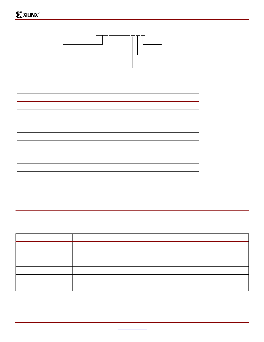
QPro Virtex 2.5V QML High-Reliability FPGAs
DS002 (v1.5) December 5, 2001
www.xilinx.com
31
Preliminary Product Specification
1-800-255-7778
R
SMD (Class Q) Odering Options
Revision History
The following table shows the revision history for this document
Date
Version
Revision
10/04/99
1.0
Initial Xilinx release.
06/01/00
1.1
Upated format.
02/13/01
1.2
Updated Temperature Specifications.
11/05/01
1.3
Changed V600 Power-up temp min to ≠55∞C. Added L33 as Bank 7 V
REF
. Updated format.
11/15/01
1.4
Fixed boken links. Added note for VCCO banking rules for PQ240 package.
12/05/01
1.5
Corrected Table 5 pin description for pin 9 and pin 39.
5962 9957201 Q Y C
Lead Finish
Generic Standard
Microcircuit Drawing (SMD)
Device Type
Package Type
QML Certified MIL-PRF-38535
(1)
Valid SMD Combinations
SMD Number
Device
Pkg Markings
Lead Finish
5962-9957201QYC
XQV300-4CB228Q
Lid
Gold Plate
5962-9957201QZC
XQV300-4CB228Q
Base
Gold Plate
5962-9957201NTB
XQV300-4PQ240N
-
Solder Plate
5962-9957201NNA
XQV300-4BG352N
-
Solder Ball
5962-9957201NUA
XQV300-4BG432N
-
Solder Ball
5962-9957301QYC
XQV600-4CB228Q
Lid
Gold Plate
5962-9957301QZC
XQV600-4CB228Q
Base
Gold Plate
5962-9957301NTB
XQV600-4HQ240N
-
Solder Plate
5962-9957301NUA
XQV600-4BG432N
-
Solder Ball
5962-9957401QXC
XQV1000-4CG560Q
-
Solder Column
5962-9957401NUA
XQV1000-4BG560N
-
Solder Ball
Notes:
1.
Type N designates QML Plastic.