 | –≠–ª–µ–∫—Ç—Ä–æ–Ω–Ω—ã–π –∫–æ–º–ø–æ–Ω–µ–Ω—Ç: YGV617B-S | –°–∫–∞—á–∞—Ç—å:  PDF PDF  ZIP ZIP |
Document Outline
- ˛ˇ
- ˛ˇ
- ˛ˇ
- ˛ˇ
- ˛ˇ
- ˛ˇ
- ˛ˇ
- ˛ˇ
- ˛ˇ

YGV617B CATALOG
CATALOG No. : LSI-4GV617B2
1998. 1
YGV617B
AVDP3
Advanced Video Display Processor 3
x
OUTLINE
YGV617B has a built-in PLL circuit which allow to superimpose the images outputted by the device over an external video
signals easier.
Since this device has a high speed drawing function and character drawing function and is able to specify vertical and hori-
zontal size of the screen optionally, it is applicable to controlling display units such as a wide screen TV and liquid crystal
displays.
These features make this device best suited to uses such as multi-vision display of automobile audio system, display of auto-
mobile navigation system, OSD of wide screen TV, video editing equipment and karaoke equipment.
This device has I/O pins for RGB (YUV) data, with which it is also suited to digital video applications such as DVD player
and set-top-boxes.
x
FEATURES
[Functions]
9 Bit map plane is able to display images simultaneously using 16 colors, 256 colors or 32768 colors.
9 A sprite is able to use 32 x 32 dots.
9 The sprite plane can be used as a crosshair line cursor.
9 A monitor synchronization frequency, dot clock frequency and display screen resolution can be specified optionally.
9 High resolution display and interlaced scanning can be used.
9 All direction smooth scroll (spherical scroll) function can be used.
9 Has a built-in color look up table of 256 words x 16 bits, where display colors can be selected from 32768 colors.
9 Linear RGB output is obtained with the built-in DAC.
9 The built-in PLL circuit enables the device to generate clock signals that is synchronized with external video signals.
9 By generating dot clock signals that are synchronized with sub carrier clock signals, the device makes clear image at an
optional resolution without misalignment of colors.
9 Provides various drawing command functions.
[CPU Interface]
9 16 bit or 8 bit asynchronous interface
9 Registers and various I/O ports are mapped on the 16 byte I/O space.
9 Video memory up to 2 Mbytes can be mapped directly on the memory space of the system.
9 Has a built-in drawing data FIFO, and CPU interrupt function.
9 When connected with an external DMA controller, command drawing data can be transferred through DMA.
[Other Features]
9 One unit of 4 M or 16 M DRAM with 16 bit configuration can be connected.
9 Since clock signals for video memory can be inputted in addition to clock signals for display, an access speed that is the
most suitable to the DRAM to be connected can be specified.
9 The built-in FIFO for display data has reduced overhead at draw data access, achieving high speed drawing.
9 Has digital RGB I/O pins, YS pin and attribute output pin.
9 144 pin plastic SQFP.
9 CMOS and 5 V single power supply
YGV617B
2
x
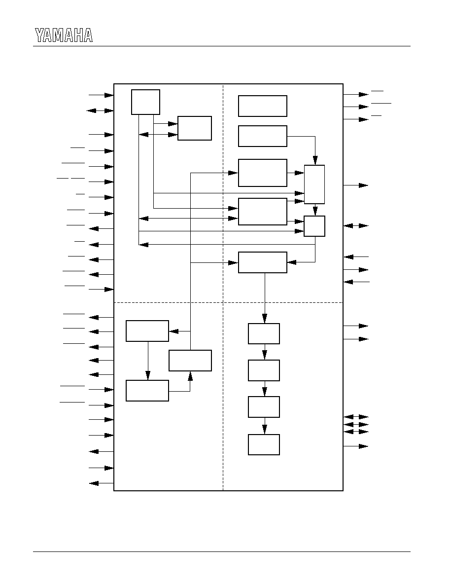
BLOCK DIAGRAM
D15-0
A20-1
LWD
CSIO
CSMEM
A0/WR1,WR0
RD
DACK
RESET
HRESET
VRESET
CTLV
DCKIN
CREF
DREQ
INT
WAIT
READY
CSYNC
HSYNC
VSYNC
DOTCK
FSC
REFOUT
DCKOUT
WE
VA9-0
VD15-0
VCKIN
VCKOUT
VCKS
YS
AT
R,G,B
DB4-0
DG4-0
DR4-0
CAS1,0
RAS
CPU
INTERFACE
VRAM
INTERFACE
COLOR
DAC
PALETTE
generator
Timing
CONTROLLER
CRT
PLL
Sync.
Generator
Scan Timing
Generator
Pixel
Shifter
Pixel Data
Buffer
DRAM
Timing Gen.
Write
Buffer
Decoder
Adrs
MUX
Data
MUX
DRAM
Bus Arbiter
Display
Generator
Address
Drawing
Unit
Processor
Color
SEL
DAC
Palette

3
YGV617B
x
PIN ASSIGNMENT
109
G
110
B
111
AVDD2
112
HRESET
113
VRESET
114
VSS
115
HSYNC
116
REFOUT
117
VDD
118
CSYNC
119
FSC
120
YS
121
AT
122
DR0
123
VSS
124
DR1
125
DR2
126
DR3
127
DR4
128
DG0
129
DG1
130
VDD
131
DG2
132
VSS
133
DG3
134
DG4
135
DB0
136
DB1
137
DB2
138
DB3
139
DB4
140
VSS
141
DCKOUT
142
DCKIN
143
VDD
144
DOTCK
73
VD7
74
VSS
75
VD8
76
VD9
77
VD10
78
VD11
79
VDD
80
VD12
81
VSS
82
VD13
83
VD14
84
VD15
85
RAS
86
WE
87
CAS0
88
VSS
89
CAS1
90
VA0
91
VA1
92
VA2
93
VSYNC
94
VDD
95
VA3
96
VA4
97
VA5
98
VSS
99
VA6
100
VA7
101
VA8
102
VA9
103
AVSS1
104
CTLV
105
CREF
106
AVDD1
107
AVSS2
R
108
VD6
72
VD5
71
VD4
70
VD3
69
VSS
68
VD2
67
VD1
66
VD0
65
VCKS
64
VDD
63
VCKOUT
62
VCKIN
61
VSS
60
LWD
59
INT
58
WAIT
57
READY
56
DREQ
55
DACK
54
CSMEM
53
CSIO
52
TEST
51
VSS
50
VDD
49
RD
48
WR0
47
A0/WR1
46
RESET
45
A20
44
A19
43
A18
42
A17
41
VSS
40
A16
39
VDD
38
A15
37
A14
36
A13
35
A12
34
A11
33
A10
32
A9
31
A8
30
A7
29
A6
28
VSS
27
A5
26
A4
24
25
VDD
23
A3
22
A2
21
A1
20
D15
19
D14
18
D13
17
VSS
16
D12
15
D11
14
D10
13
D9
12
D8
11
VSS
10
VDD
9
D7
8
D6
7
D5
6
D4
5
D3
4
VSS
3
D2
2
D1
1
D0
TOP VIEW
YGV617B
4
x
PIN FUNCTIONS
<CPU interface>
9
D15-0 (I/O : Pull Up)
These pins comprise a CPU data bus. D15-D8 pins are to be kept open in case of 8 bit CPU that does not use the pins.
9
A20-1 (I)
These pins comprise a CPU address bus. Input to A20-4 pins is ignored when accessing CSIO space. Unused pins are
to be pulled up or down.
9
CSIO (I)
This is a chip select signal input for determining I/O space. An I/O port in AVDP3 is accessed by the write/read puls-
es that are inputted when this signal is active. When the address is inputted with this signal at low level, input to A20-
4 pins is ignored.
9
CSMEM (I)
This is a chip select signal input for determining video memory port. Video memory controlled by AVDP3 is directly
accessed by the write/read pulses that are inputted when this signal is active. The video memory can also be accessed
from I/O space without using this pin if a high level signal is inputted to this pin.
9
A0/WR1, WR0 (I)
These signals are used to control writing into AVDP3 when the chip select input is active. A0/WR1 controls D15-8,
and WR0 controls D7-D0.
In case of 8 bit CPU, A0/WR1 functions as the CPU address bit 0.
9
RD (I)
This signal controls reading from AVDP3 when the chip select input is active. D15-0 pins are in output state in the
period where both this signal and the chip select signal are active.
9
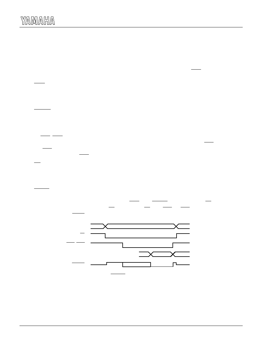
READY (O : Pull Up, 3 state output)
This is the data ready signal output to CPU. When internal state of AVDP3 becomes accessible, this signal becomes
active. This pin becomes high impedance state when CSIO pin or CSMEM pin (hereafter called CS pin) is not active,
or this pin outputs high level signal when CS pin is active and RD or A0/WR1 and WR0 pins are not active.
Some CPU must use WAIT signal instead of this signal.
Hi-Z
Hi-Z
CS
A0/WR1,WR0
D15-0
A6-1
READY
VALID
VALID
State of READY signal at write access

5
YGV617B
9
WAIT (O : Pull Up, 3 state output)
This is the data wait signal outputted to CPU. When CS pin is active, this pin outputs WAIT signal responding to the
RD or A0/WR1 and WR0 signals, and then clears the WAIT signal when the CPU has become accessible.
When CS pin is not active, this pin becomes high impedance state.
When CS pin is active and RD or A0/WR1 and WR0 pins are not active, the level of this pin becomes high.
Some CPU must use READY signal instead of this signal.
State of WAIT signal at write access
9
INT (O : Open drain output)
Outputs an interrupt request signal to CPU. This signal becomes active when the internal state of AVDP3 coincides
with the conditions set in the registers. It is reset when registers of AVDP3 have been accessed.
9
LWD (I)
This signal selects the width of data bus according to CPU. When high level signal is inputted, this device complies
with 16 bit system, or when low level signal is inputted, it complies with 8 bit system.
9
RESET (I : Pull Up)
This pin accepts an initial reset signal. Internal registers of AVDP3 is cleared to "0" when this signal has been
inputted. (Some registers are loaded with initial value.) Make sure to input the reset signal at power on.
9
DREQ (O)
Outputs command data request signal to an external DMA controller.
9
DACK (I : Pull Up)
When an external DMA controller has received DREQ signal, it returns command data transfer permit signal to this
device through this pin.
<Video Memory Interface>
9
VA9-VA0 (O)
These pins comprise an address bus for VRAM. This bus outputs low address and column address of DRAM used by
AVDP3 based on time sharing. This pin becomes high impedance when in VRAM halt state.
9
VD15-VD0 (I/O : Pull Up)
These pins comprise an data bus for VRAM. Data of DRAM used by AVDP3 are transferred through this bus. This
pin becomes high impedance when in VRAM halt state.
9
RAS (O)
This pin outputs DRAM row address strobe signals for VRAM. This pin becomes high impedance when in VRAM
halt state.
9
CAS1,0 (O)
These pins output DRAM column address strobe signals for VRAM. CAS1 and CAS0 are respectively related to data
buses VD15-8 and VD7-0. These pins become high impedance when in VRAM halt state.
Hi-Z
Hi-Z
CS
A0/WR1,WR0
D15-0
A6-1
WAIT
VALID
VALID