 | –≠–ª–µ–∫—Ç—Ä–æ–Ω–Ω—ã–π –∫–æ–º–ø–æ–Ω–µ–Ω—Ç: YGV627 | –°–∫–∞—á–∞—Ç—å:  PDF PDF  ZIP ZIP |

YGV627 CATALOG
CATALOG No.: LSI-4GV627A2
2001.01
YGV627
AVDP3E
Advanced Video Display processor 3 Enhanced
s
OUTLINE
YGV627 is a VDP (Video Display Processor) that realizes higher resolution, multi-color and high speed drawing
by adopting a synchronous DRAM as the video memory, while maintaining the register compatibility with
YGV617B that is used for controlling the high minuteness On Screen Display (OSD).
Since the device is capable of displaying bitmap images with various resolutions ranging from NTSC to SVGA on
the monitors with any size of screen including wide screen, it can be used for controlling OSD for various display
units. Also, it is capable of representation of varied images in accordance with the application because numerous
number of colors can be selected such as the one in the range from 16 to 65536 RGB color display, or natural image
display using YCbCr.
In addition, the existing system can be up-graded easily thanks to the basic features from YGV617B such as a high
speed drawing function, character drawing function, synchronization with external video signal, digital video input /
output function, and hardware cursor display function.
s
s
s
s
FEATURES
YGV627 is capable of selecting two modes by using the setting of
ENH
pin.
For convenience, the case of using
ENH
pin with LOW level (enabled) is referred to as "expansion mode" in this
document. In the expansion mode, all the functions can be used.
The case of using
ENH
pin with HIGH level (disabled) is referred to as "compatibility mode". In the compatibility
mode, the software compatibility with YGV617B is maintained, but the functions enhanced for YGV617B cannot
be used. These modes should be used in accordance with the purpose of the application of this device.
[Display functions]
q
Three screen configuration including bitmap screen, sprite cursor screen and external input video screen
(or single color border screen)
q
Monitor synchronization frequency, dot clock frequency, and display screen resolution can be specified optionally.
q
Display dot clock up to 40 MHz (Example of resolution: NTSC, PAL, VGA, SVGA, NTSC wide, and VGA wide)
q
Support with progressive scanning and interlaced scanning
q
Resolution of sprite cursor screen is 32
X
32 dots. (The sprite cursor can also be used as cross-hair line cursor.)
q
Smooth hardware scroll function
q
Upper / lower two division display on the bitmap screen (The two sections can be scrolled independently).
q
256 word
X
16 bit CLUT is built-in (The number of display colors of 32768 colors or 65536 colors can be selected.)
q
Display colors: 16 palette color, 256 palette color, 32768 RGB color, 65536 RGB color, YCbCr422 (ITU601)
q
YCbCr (ITU601) -to-8 bit RGB decoder is built-in.
q
blending function that mixes with external input screen or single color border screen. (64 intensity levels)
q
Dot clock generation with built-in PLL circuit
q
Generates dot clock that synchronizes with HSYNC of external video signal.
q
Generates dot clock that synchronizes with external input clock. (such as sub-carrier clock)
YGV627
2
[Drawing functions]
q
Commands
Block transfer by word (CPU to VRAM, VRAM to CPU, VRAM to VRAM)
Font drawing, dot drawing and rectangular drawing.
q
Drawing attribute
Sets drawing clip area, drawing offset or drawing page, and designates bit mask, color mask,
logical operation (NOT, AND, OR, EOR etc.), or direction of transfer.
[Operational clock]
q
System clock (clock for drawing system):
up to 33 MHz
q
Dot clock (clock for display system):
up to 40 MHz
[CPU interface]
q
16 bit or 8 bit asynchronous interface
q
Provided with a video memory space up to 8M bytes and internal register space of 128 bytes.
q
The video memory space and internal register space can be mapped indirectly with 16 byte registers.
q
Built-in data buffer for memory space access and built-in data FIFO for drawing commands
q
CPU interruption based on various conditions of display and drawing
q
DMA transfer of drawing command data can be made when connected with external DMA controller
[Video memory interface]
q
Connected memory:
16M bit SDRAM (512k words
X
16 bits
X
2 banks) 1 piece
or 64M bit SDRAM (1M words
X
16 bits
X
4 banks) 1 piece
q
SDRAM clock:
up to 66 MHz (System clock multiplied by 2 or 4)
q
Built-in FIFO for display data improves the drawing access efficiency and realizes high speed drawing.
[Monitor interface]
q
Analog RGB output with built-in DAC (8 bits for RGB individually)
q
Digital video input / output (6 bits for RGB individually)
q
Equipped with sub-carrier clock output, dot clock output, sync signal output, YS and attribute output pins.
[Others]
q
Package: 176LQFP (YGV627-V)
q
CMOS, 3.3V single power supply
q
Operating temperature range:
-
40 to +85
∞
C
Supplementary information:
For YGV627, Application Manual that details the specifications of the device and the evaluation board
(MSY627DB01) are available in addition to this brochure.
The evaluation board is equipped with an SDRAM of 8 MB as a video memory. A high performance system can
be realized when it is used with Hitachi's CPU board, Super H Solution Engine.
The device driver provided by Yamaha and attached to the evaluation board
consists of the main body of the driver and API related layers, allowing the
user to build it into the system easily according to the environment.
For the details of these products, inquire of the sales agents or our business
offices.
For CPU board, inquire of: Hitachi ULSI Systems Co., Ltd.
Tel:+81-42-351-6600

YGV627
3
s
s
s
s
BLOCK DIAGRAM
Drawing
command
CPU
Memory
control
Sync.
control
PLL
Display
control
Screen
synthesis
Digital video
input
Analog
RGB
YGV627
OSD screen
CPU
Interface
SDRAM
16Mbit
16
16
TFT
Panel
Digital video output
(Also used as digital video
input pin)
DAC
YGV627 is connected to the external memory bus of CPU as an external I/O device. As a video memory, SDRAM of up
to 64M bits can be connected to local memory bus of YGV627 to send bitmap image data stored in the video memory into
monitor as RGB signal in accordance with display scan timing.
YGV627 stores image data from CPU to the video memory by accessing video memory directly through CPU interface
or by accessing the video memory using internal drawing command that transfers the data by block.
YGV627 has a function that synthesizes external images with bitmap image of YGV627 on the screen by synchronizing
the scan timing of YGV627 with display timing of external video signals.
YGV627
4
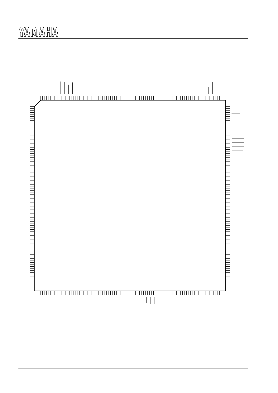
s
PIN ASSIGNMENT
TOP VIEW
CAS
NC
VDD
VSS
VSS
VDD
VD2
VD14
VD1
VD15
VD0
VD6
VDD
VD10
VD5
VD11
VD4
VD12
VSS
VD3
VD13
BA0
DQMH
DQML
VD8
VSS
VD7
VD9
VDD
SDCLK
VSS
BA1
VA11
VA0
VA8
VA10
VA9
NC
VA1
VA7
VSS
V D D
V S S
V S S
V D D
V A 4
V A 3
V A 5
V A 2
V A 6
N C
D O T C L K
D V 6
D V 5
D V 4
D V 3
D V 2
D V 1
D V 0
D V 1 5
D V 1 4
D V 1 3
D V 1 2
V D D
D V 1 1
D V 1 0
D V 9
D V 8
V S S
D V 7
V D D
A T
Y S
F S C
V S S
D V 1 7
D V 1 6
N C
V S S
NC
VSS
VDD
SYCKIN
SYCKOUT
DTCKIN
DTCKOUT
AVDD2
DPLLFILT
DPLLRREF
DPLLVSSR
AVSS2
AVSS3
R
G
B
IREF
AVDD3
LWD
A0/
AVDD1
SPLLFILT
SPLLRREF
SPLLVSSR
AVSS1
NC
A4
A3
A2
A1
N C
A 1 4
A 1 3
A 1 2
A 1 1
A 1 0
A 9
A 8
A 7
A 6
A 5
A 2 1
A 2 0
A 1 9
A 1 8
A 1 7
A 1 6
A 1 5
D 0
V D D
V S S
A 2 2
D 1 3
D 1 2
D 1 1
D 1 0
D 9
D 8
V S S
D 7
D 6
D 5
D 4
D 3
D 2
N C
D 1 5
D 1 4
D 1
1
11
10
9
8
7
6
5
4
3
2
21
20
19
18
17
16
15
14
13
12
28
27
26
25
24
23
22
34
33
32
31
30
29
42
41
40
39
38
37
36
35
44
43
45
55
54
53
52
51
50
49
48
47
46
65
64
63
62
61
60
59
58
57
56
72
71
70
69
68
67
66
78
77
76
75
74
73
86
85
84
83
82
81
80
79
88
87
13 2
12 2
12 3
12 4
12 5
12 6
12 7
12 8
12 9
13 0
13 1
11 2
11 3
11 4
11 5
11 6
11 7
11 8
11 9
12 0
12 1
10 5
10 6
10 7
10 8
10 9
11 0
11 1
9 9
10 0
10 1
10 2
10 3
10 4
9 1
9 2
9 3
9 4
9 5
9 6
9 7
9 8
8 9
9 0
176
166
167
168
169
170
171
172
173
174
175
156
157
158
159
160
161
162
163
164
165
149
150
151
152
153
154
155
143
144
145
146
147
148
135
136
137
138
139
140
141
142
133
134
R E A D Y
D R E Q
W A I T
I N T
I N T 2
WE
RAS
CS
B L A N K
H S Y N C
V S Y N C
C S Y N C
H S I N
V S I N
DVOUT
ENH
TEST2
TEST1
TEST0
SYSEL
RD
WR0
DMAP
RESET
CSREG
CSMEM
DACK
VR64
WR1
YGV627
5
s
PIN FUNCTIONS
<CPU interface>
q
q
q
q
D15
-
-
-
-
0 ( I/O: PULL UP )
This is a data bus for connecting with external processor. D15
-
D8 are not used when the CPU bus with 8 bit type
(when low level is inputted to LWD). At this time, keep the D15
-
D8 open. These pins are provided with pull-up
resistors respectively.
q
q
q
q
A22
-
1 ( I )
This is an address bus to be connected with external general purpose microcomputer. In the indirect access mode
(high level inputted to
DMAP pin), input to A22
-
A4 pins are ignored when accessing
CSREG space.
In the direct access mode (low level inputted to
DMAP pin), input to A22
-
A8 pins are ignored when accessing
CSREG space.
YGV627 can be used as a YGV617B compatible device when A22 and A21 pins are fixed to low level. Unused pins
must be set to low level or high level.
q
q
q
q
CSREG ( I )
It is a chip select signal input to register space (I/O). When this chip select signal is active, the read / write pulses
inputted are made valid so that the registers in the YGV627 are accessed.
The function of this pin is the same as that of
CSIO pin of YGV617B.
q
q
q
q
CSMEM ( I )
This is a chip select signal input pin for video memory port. The read / write pulse inputted while this signal is active
can be used to directly access the video memory controlled by YGV627.
It is possible not to use
CSMEM because the video memory can also be accessed from registers. In such case, it is
necessary to input high level to CSMEM pin.
q
q
q
q
A0
/
WR1, WR0 ( I )
When chip select input is active, these pins control write access to YGV627.
D15
-
D8 are controlled by
A0
/
WR1, and D7
-
D0 by
WR0.
When the CPU is 8 bit type,
A0
/
WR1 functions as CPU address bit 0.
q
q
q
q
RD ( I )
When chip select input is active,
RD controls read access from YGV627.
D15
-
D0 are in Output State in the period while both this signal and chip select signals are active.
q
q
q
q
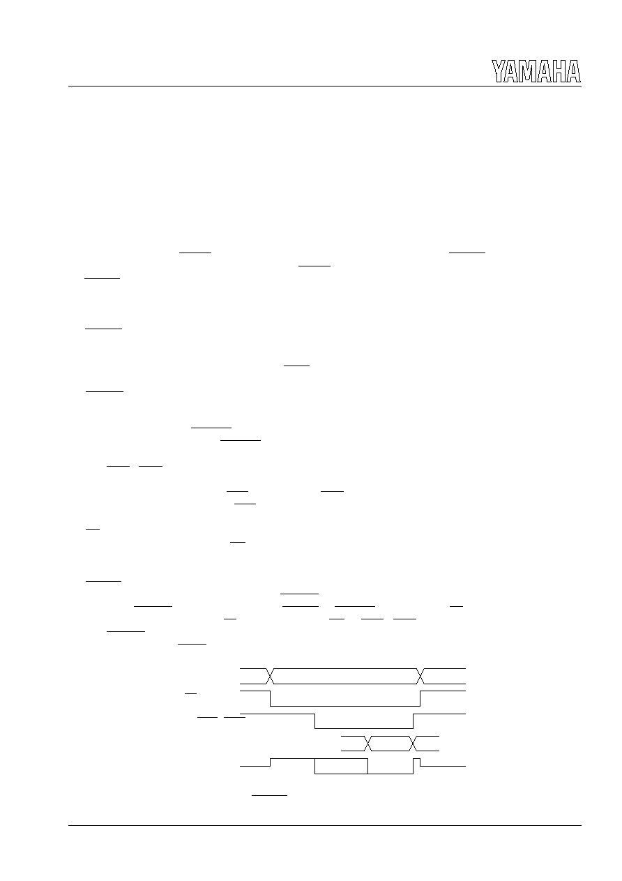
READY ( O: PULL UP, 3-state output )
This is data ready signal output to CPU. The
READY signal is made low when the internal state of YGV627 is
accessible.
READY is a 3-state output. When CSREG or CSMEM (hereafter called CS signals) is not active, it is
high impedance state, and when
CS signals is active and RD or WR1, WR0 is not active, high level is outputted
from
READY.
Some CPU must use
WAIT signal instead of this signal.
A22-A1
CS
A0/WR1, WR0
D15-D0
READY
ØØØØØØ
VALID
VALID
Hi-Z
Hi-Z
READY signal at write access