YMF715E
OPL3-SA3
OPL3 Single-chip Audio System 3
YAMAHA CORPORATION
May 21, 1997
Preliminary
OUTLINE
YMF715E-S (OPL3-SA3) is a single audio chip that integrates OPL3 and its DAC, 16bit Sigma-delta
CODEC, MPU401 MIDI interface, joystick port, and a 3D enhanced controller including all the analog
components which is suitable for multi-media application. This LSI is fully compliant with Plug and Play
ISA 1.0a, and supports all the necessary features, i.e. 16bit address decode, more IRQs and DMAs in
compliance with PC'96. This LSI also supports the expandability, i.e. Zoomed Video, Modem and CD-
ROM interface in a Plug and Play manner, and power management (power down, power save, partial
power down, and suspend/resume) that is indispensable with power-conscious application.
FEATURES
Built-in OPL3 (FM-synthesizer)
Supports Sound Blaster Game compatibility
Supports Windows Sound System compatibility
Supports Plug & Play ISA 1.0a compatibility
Full Duplex operation
Built-in MPU401 Compatible MIDI I/O port
Built-in Joystick port
Built-in the 3D enhanced controller including all the analog components
Supports multi-purpose pin function
(Support 16-bit address decode, DAC interface for OPL4-ML/ML2, Zoomed Video port, EEPROM
interface, MODEM interface, IDE CD-ROM interface)
Hardware and software master volume control
Supports monaural input
24 mA TTL bus drive capability
Supports Power Management(power down, power save, partial power down, and suspend/resume)
+5V/ +3.3V power supply for digital, 5V power supply for analog.
100 pin SQFP package (YMF715E-S)
The contents of this catalog are target specifications and are subject to change
without prior notice. When using this device, please recheck the specifications.
YMF715E
May 21, 1997
-4-
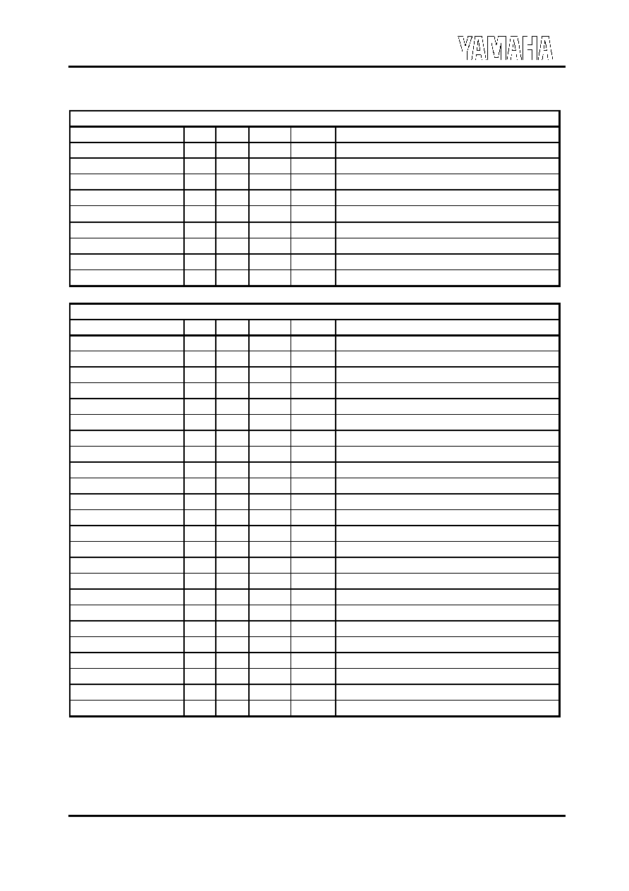
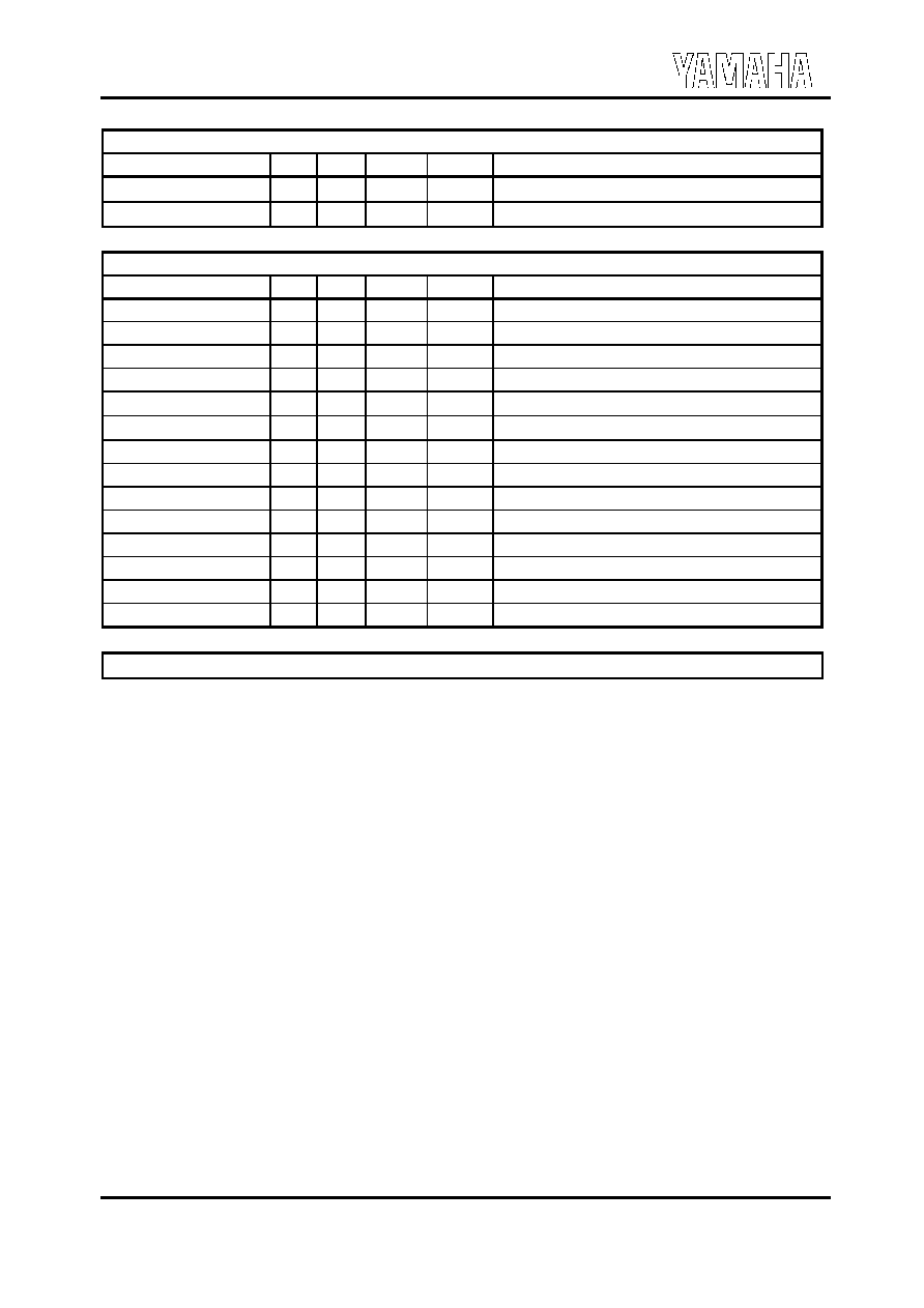
Multi-purpose pins : 13 pins
name
pins
I/O
type
size
function
SEL2-0
3
I+
CMOS
-
Refer to "Multi-purpose pins" section
MP9-0
10
I+/O
TTL
2mA
Refer to "multi-purpose pins" section
Others : 27 pins
name
pins
I/O
type
size
function
GP3-0
4
IA
-
-
Game Port
GP7-4
4
I+
Schmitt
-
Game Port
RXD
1
I+
Schmitt
-
MIDI Data Receive
TXD
1
O
TTL
4mA
MIDI Data Transfer
/VOLUP
1
I+
Schmitt
-
Hardware Volume (Up)
/VOLDW
1
I+
Schmitt
-
Hardware Volume (Down)
X33I
1
I
CMOS
-
33.8688 MHz
X33O
1
O
CMOS
2mA
33.8688 MHz
X24I
1
I
CMOS
-
24.576 MHz
X24O
1
O
CMOS
2mA
24.576 MHz
AVDD
2
-
-
-
Analog Power Supply (put on +5.0V)
DVDD
3
-
-
-
Digital Power Supply (put on +5.0 V or +3.3V)
AVSS
2
-
-
-
Analog GND
DVSS
4
-
-
-
Digital GND
Total : 100 pins
Note :
I+:
Input Pin with Pull up Resistor
T: TTL-tri-state output pin
Schmitt:
TTL-Schmitt input pin