
YMU762
MA-3
Mobile Audio 3
YAMAHA CORPORATION
YMU762 CATALOG
CATALOG No.:LSI-4MU762A3
2002.9
Outline
MA-3 is a synthesizer LSI for mobile phones that realize advanced game sounds.
This LSI has a built-in speaker amplifier, and thus, is an ideal device for outputting sounds that are used by mobile
phones in addition to game sounds and ringing melodies that are replayed by a synthesizer.
The synthesizer section adopts "stereophonic hybrid synthesizer system" that are given advantages of both FM
synthesizers and Wave Table synthesizers to allow simultaneous generation of up to thirty two FM voices and eight
Wave Table voices.
Since FM synthesizer is able to present countless voices by specifying parameters with only several tens of bytes,
memory capacity and communication band can be saved, and thus, the device exhibits the features in operating
environment of mobile phones such as allowing distribution of arbitrary melodies with voices.
On the other hand, Wave Table synthesizer can pronounce the voice built in ROM and arbitrary ADPCM/PCM voices
from sequencer by the download of the melody with voices etc..
MA-3 has a built-in hardware sequencer that helps to realize complex play without heavily loading the host CPU.
The device also has a built-in circuit for controlling vibrators and LEDs synchronizing with play of music.
Features
MA-3 has features as described below.
Simultaneous generation of up to 40 tones: FM + Wave Table stereophonic hybrid synthesizer.
Polyphonic synthesizer specification.
Has built-in default voices for FM and Wave Table synthesizers in the ROM, and the voices can be downloaded to
RAM.
Fundamental waveforms for FM and algorithm are improved compared with YMU759 (MA-2), and voice
parameters of detune etc. are added.
Stream replay with ADPCM / PCM (shared use of Wave Table section).
Software interrupt mechanism for external synchronization.
Equipped with 8 bit parallel I/F for control from CPU.
Equipped with speaker amplifier and equalizer circuit.
Equipped with vibration control circuit, and LED lighting control circuit.
Has built-in PLL to support inputting of master clock up to 20 MHz.
Contains
a
16-bit stereophonic D/A converter.
Equipped with a stereophonic output terminal for headphone.
Supports power down mode.
Digital power supply: 2.7V to 3.3V (Typ 3.0V)
Analog power supply: 2.7V to 4.5V (Typ 3.6V)
32-pin QFN plastic package
The contents of this booklet are target specifications and they are subject to change without
a prior notice. Please check the finalized specifications before actually using this LSI.

YMU762
2
Pin configuration
16
15
14
13
12
11
10
SPVSS
SPVDD
EQ3
EQ2
EQ1
HPOUT-R
HPOUT-L/M ONO
VRE
F
VS
S
VDD
PLLC
N.
C
/R
S
T
/I
R
Q
LED
CL
K
I
SPO
U
T
1
SPO
U
T
2
MT
R
D7
D6
D5
D4
D3
D2
26
27
28
29
30
31
32
D1
D0
/W R
/CS
A0
/RD
IOVDD
25
24
23
22
21
20
19
18
17
1
2
3
4
5
6
7
8
9
<32pin QFN Top View>

YMU762
3
Functions of pins
No.
Pin name
I/O
Power supply
Function
1
CLKI
Ish
IOVDD
Clock input ( 2 MHz to 20 MHz)
2
LED
O
IOVDD
External LED control (Drive Capability = 4 mA)
3
/IRQ
O
IOVDD
Interrupt output (Drive Capability = 1 mA)
4
/RST
Ish
IOVDD
Hardware reset input
5 N.C
No Connection (during regular operations)
6 PLLC A VDD
Connection of capacitor for built-in PLL
Connect a series connection of 1000 pF capacitor and 3.3 k resistor
between this pin and VSS(*).
(*)Directly connect VSS used here and VSS of 8
th
pin.
7 VDD
Power supply (Typ +3.0V)
Connect 0.1 �F and 4.7 �F capacitors between this pin and VSS.
8 VSS
Ground
9 VREF A VDD
Analog reference voltage
Connect 0.1 �F capacitor between this pin and VSS.
10
HPOUT-L /
MONO
A
VDD
Headphone output Lch (Can be used as MONO output)
11
HPOUT-R
A
VDD
Headphone output Rch
12 EQ1 A VDD Equalizer
pin
1
13
EQ2
A
VDD
Equalizer pin 2
14
EQ3
A
VDD
Equalizer pin 3
15 SPVDD
Speaker amplifier analog power supply (Typ +3.6V)
Connect 0.1 �F and 4.7 �F capacitors between this pin and SPVSS.
16 SPVSS
Speaker amplifier analog ground
17 SPOUT1
A
SPVDD
Speaker connection pin 1
18
SPOUT2
A
SPVDD
Speaker connection pin 2
19
MTR
O
IOVDD
External motor control pin (Drive Capability = 4 mA)
20
D7
I/O
IOVDD
CPU I/F data bus 7 (Drive Capability = 1 mA)
21
D6
I/O
IOVDD
CPU I/F data bus 6 (Drive Capability = 1 mA)
22
D5
I/O
IOVDD
CPU I/F data bus 5 (Drive Capability = 1 mA)
23
D4
I/O
IOVDD
CPU I/F data bus 4 (Drive Capability = 1 mA)
24
D3
I/O
IOVDD
CPU I/F data bus 3 (Drive Capability = 1 mA)
25
D2
I/O
IOVDD
CPU I/F data bus 2 (Drive Capability = 1 mA)
26 D1
I/O
IOVDD
CPU I/F data bus 1 (Drive Capability = 1 mA)
27
D0
I/O
IOVDD
CPU I/F data bus 0 (Drive Capability = 1 mA)
28
/WR
I
IOVDD
CPU I/F write enable
29
/CS
I
IOVDD
CPU I/F chip select
30
A0
I
IOVDD
CPU I/F address signal
31
/RD
I
IOVDD
CPU I/F read enable
32 IOVDD
Pin power supply (Typ +3.0V)
Be sure to apply potential equivalent to 7
th
pin (directly connect on the
board).
A : Analog pin Ish : Schmitt input

YMU762
4
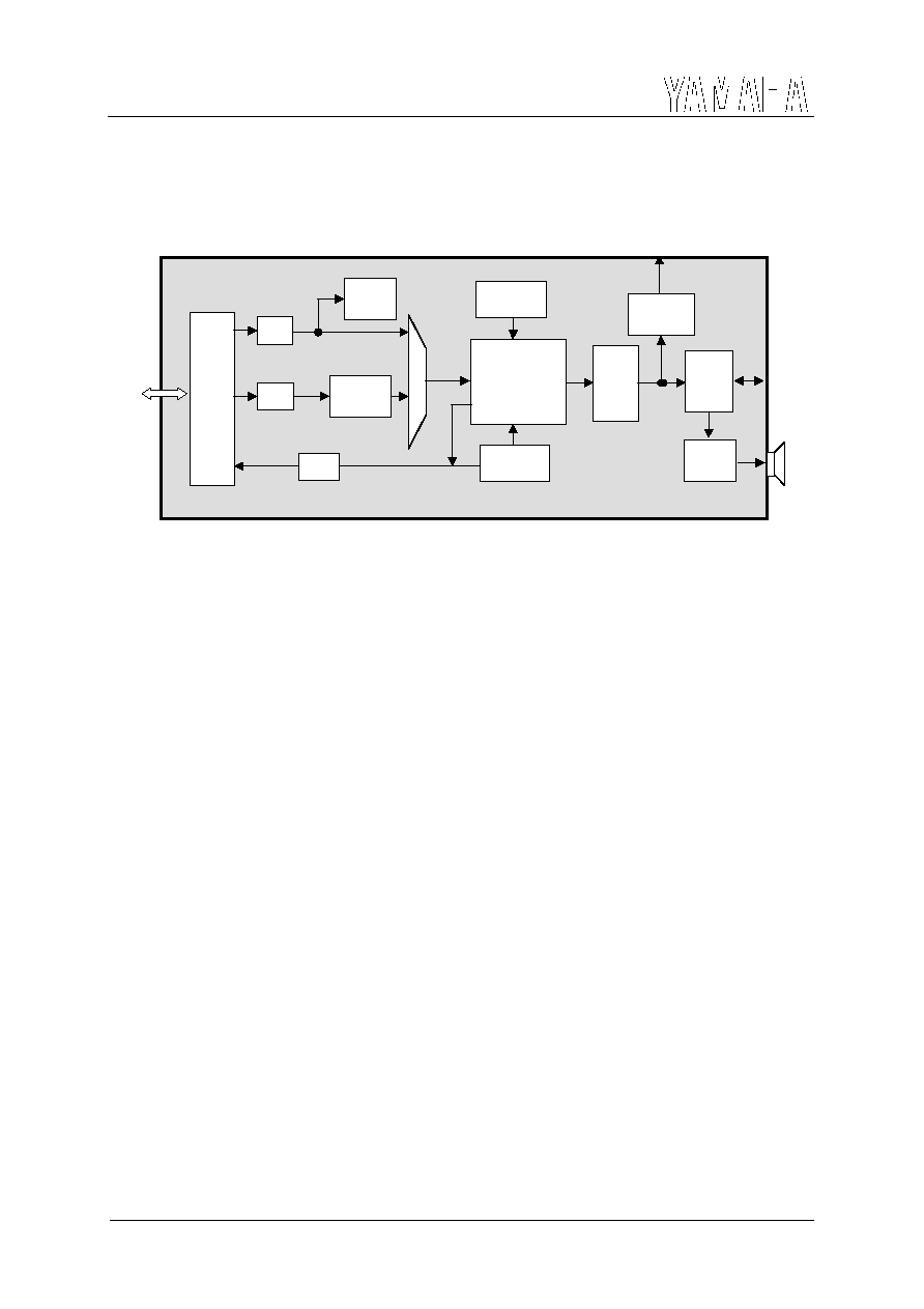
Block diagram
HPOUT-L
/MONO
HPOUT-R
1
6-
bit
DAC
Lc
h
Rc
h
CLKI
VDD
VSS
PLLC
CP
U
I/
F
Po
w
e
r
Down
C
ont
r
o
l
T
i
ming G
e
ner
a
tor
PLL
/I
R
Q
LED
MT
R
L
E
D
contr
o
l
Vibr
ator
c
ont
r
o
l
TIM
E
R
A0
/WR
/R
D
D0 -
D7
/C
S
EQ
1
SPVDD
SPVSS
EQ
2
EQ
3
VR
E
F
+
VRE
F
VRE
F
SP
Vol
S
P
OUT
1
S
P
OUT
2
Analog power
Supply dedicated
To speaker amp
M
ono
SR
A
M
8k-
byt
e
Voice
RO
M
Rc
h
Lc
h
EQ
Vol
IOVDD
Re
g
i
st
e
r
Sequencer
SE
Q
FI
FO
5
1
2byte
I
n
s
t
ant
a
ne
ous
pa
th
FI
FO
64byte
Select
B
u
ffe
r
HP
Vo
l
R
In
st
an
ta
n
e
ou
s
w
r
ite
p
a
th
De
l
a
y
e
d wr
i
t
e
pa
t
h
In
s
t
an
ta
n
e
o
u
s rea
d
pa
t
h
So
f
t
wa
r
e
Ir
q
F
M
+
W
a
v
etable
S
ynthes
i
z
e
r
(
F
s
=
48kHz)
P
C
M
/ADPCM
P
l
ay
b
a
ck
HP
Vo
l
L
/R
ST
YMU762
5
Outline of blocks
This section outlines functions of blocks contained in this device and flow of signals.
C
P
U
i
n
te
rfa
c
e
FIFO
Sequencer
Register
SE
L
FM +WaveTable
Synthesizer
Voice ROM
SRAM
Buffer
DAC
EQ
amp.
Speaker
amp.
Headphone
Output
Instantaneous write path
Delayed write path
Instantaneous read path
FIFO
CPU interface
CPU interface is an 8-bit parallel type.
- "Instantaneous write path" that enables Write command immediately (equipped with 64byte FIFO),
- "Delayed write path" that enables Write command after elapse of specified time, and
- Instantaneous read path
are available.
Hardware sequencer and FIFO
The sequencer is a block that controls time and register access.
The structure of sequence data includes "time information data + MA-3 register control data", for which 512 byte FIFO
is provided. The sequence data is written into delayed write path.
FM+Wave Table synthesizer
This device contains a Polyphonic synthesizer that adopts FM +Wave Table stereophonic hybrid system that generates
up to 40 tones.
The FM synthesizer has two operation modes; "16-Voice 4 operation mode" and "32-Voice 2 operation mode" which
can be changed to each other freely (except during tone generation).
Since waveform for FM operation can be set arbitrarily, the device is able to create voices that are more complex than
by conventional devices.
Wave Table synthesizers is able to generate eight voices simultaneously, and supports 8 bit PCM and 4 bit ADPCM
data format. The sampling frequency is 48 kHz. Stream replaying is also available, realizing interchangeability with
ADPCM replay capability of MA-2.
Voice ROM and SRAM
This device stores voice parameters (GM 128 voices + DRUM 40 voices) for FM and waveform data for Wave Table in
the ROM. SRAM is used when downloading arbitrary FM voice parameter and waveform data for Wave Table. It is
also used as waveform data buffer at stream replay with PCM/ADPCM.
DAC
Converts digital signal from a synthesizer into analog signal. The data length is 16 bit.
IRQ and TIMER
This device supports FIFO, two hardware TIMERs, and interrupt output with software interrupt.