
YSD917
CATALOG No: LSI-4SD917A3
2003.3
YSD917
DIR5
Digital Audio Interface Receiver 5
Outline
YSD917 is an LSI that receives and demodulates signals with the digital audio interface format that
conform to EIAJ CP1201 and IEC958 standards (hereafter referred to as "DAIF signal").
This LSI can be used for to various application such as AV amplifiers because it is capable of accepting
DAIF signal which sampling frequency ranges from 32 kHz to 96 kHz and the demodulated serial data
output is capable of being selected from various formats.
Features
[Fundamental Functions]
� Sampling frequency : Two ranges are available including;
32 kHz to 48 kHz (hereafter referred to as "normal rate") and
64 kHz to 96 kHz (hereafter referred to as "double rate")
� Can select and provide various clocks to peripheral devices such as DAC and ADC as a master clock.
� Can supply clock to ADC and DAC in any case including when DAIF signal is not present.
� The device checks the DAIF signal at all times including when it supplies clock to ADC. Thus, it is capable
of reading status information as necessary.
� Has a terminal that outputs a signal indicating the double rate operation.
� Every channel status and user data can be read through the microcomputer interface.
� Has an output terminal for interrupt that informs external devices of the changes of the status information.
� Can be adaptable to various serial data output formats by setting a register.
� The relationship between the word clock and data is maintained at all times including the moment of
transfer from PLL unlock to lock or lock to unlock so that the effect of the transfer to peripheral devices
is suppressed.
� Two or more devices can be used synchronously when in the slave mode.
[Other features]
� Microcomputer interface with four wire serial system.
� Internal operating frequency of 25 MHz
� Power down mode
� Single power supply voltage of 5.0 V
� Si-gate CMOS process
� 28 pin SOP package (YSD917-M)
YSD917
2
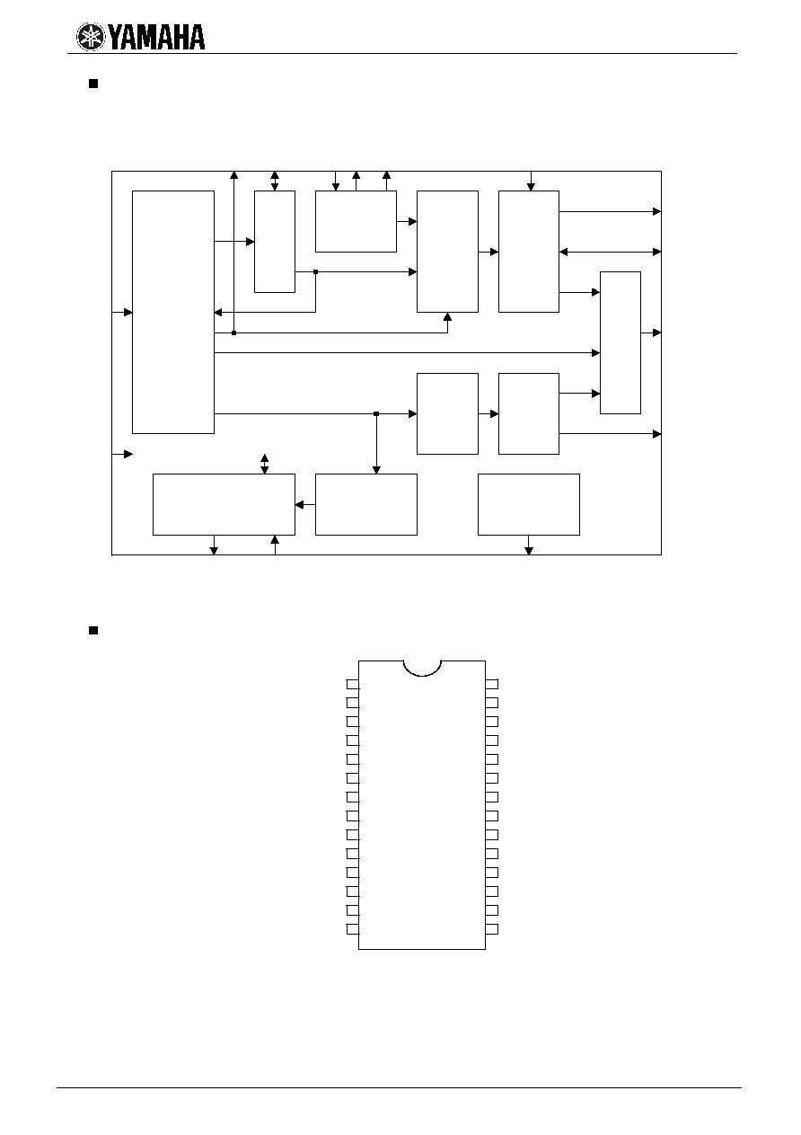
Block Diagram
D
i
git
a
l audio int
e
rf
ace
deco
der and
lock
er
ror
judgem
ent
Microcomputer interface
PLL
Reference clock
generation
Channel status
User data
Frame
buffer
Interrupt cause
detection
Clock
system
selection
Output clock
generation
Serial
Conversion
Control
signals
DATA BUS
O
u
tpu
t
se
l
e
cti
o
n
DDIN
PC
O
SDMCK
IN
T
XI
XO
SDO
ERR/BS
DBL/V
SYNC/U
FS128/C
SI
SC
K
/C
S
SO
MC
K
/IC
SDBCK
SDWCK
M/
S
/L
O
C
K
AVDD
PCO
AVSS
M/S
1
2
3
4
MCK
11
TEST
6
DDIN
5
/IC
7
VSS
8
XO
9
XI
10
VDD
12
SDO
13
SDBCK
14
SCK
SI
SO
/CS
28
27
26
25
SYNC/U
18
INT
23
VDD
24
/LOCK
22
ERR/BS
21
DBL/V
20
FS128/C
19
VSS
17
SDMCK
16
SDWCK
15
< 28pin SOP Top View >
Pin Assignment

YSD917
3
Terminal Function List
No. Name I/O
Function
1 AVDD -
Analog power supply for PLL (+5V)
2 PCO A
PLL filter connection terminal
3 AVSS -
Analog ground
4 M/S Is+
Master/slave mode selection
5 DDIN I
s
Digital audio interface data input
6 TEST I
s
+
Test terminal (To be open.)
7 /IC I
s
Initial clear input
8 VSS -
Ground
9 XO O
24.576MHz crystal oscillator connection terminal (output)
10 XI I
24.576MHz crystal oscillator connection terminal (input)
11 MCK O
12.288MHz clock output
12 VDD -
+5 V power supply
13 SDO O
Serial data output
14 SDBCK I
s
/O
Serial data bit clock input/output 64 fs
15 SDWCK I/O
Serial data word clock input/output
fs
16 SDMCK O
Serial data master clock output
256 fs or 128 fs
17 VSS -
Ground
18 SYNC/U O
Serial data synchronization timing output / User data output
19 FS128/C O
Serial data master clock 128 fs output
/ Channel status output
20 DBL/V O
Double rate output
/ Validity flag output
21 ERR/BS O
Data error detection output
/ Block start output
22 /LOCK O
PLL lock detection output
23 INT O
Interrupt output
24 VDD -
+5 V power supply
25 /CS I
Microcomputer interface chip select input
26 SO O
t
Microcomputer interface data output
27 SI I
Microcomputer interface data input
28 SCK I
s
Microcomputer interface bit clock input
Note
I
s
: Schmidt trigger input terminal
I+
: Input terminal with pull-up resistor
O
: Digital output terminal
O
t
: Three-state digital output terminal
A
: Analog terminal
For SYNC/U, FS128/C, DBL/V and ERR/BS, their functions are selected by setting a register.
YSD917
4
Terminal Function
1. System clock
:
XI, XO, MCK SDMCK
The crystal oscillator (24.576 MHz) is connected to the terminals XI and XO to form an oscillation
circuit.
Use the crystal oscillator of fundamental mode.
When using an external clock, input it to XI terminal.
This LSI supplies a master clock to the peripheral devices such as DAC, ADC and DSP.
MCK outputs the clock of 12.288 MHz (i.e. 256fs when fs=48 kHz) that is obtained by dividing the clock of XI.
For SDMCK, the operation is selected depending on the state of the PLL lock and the setting of a control
register.
When PLL is not locked (/LOCK=H) ----------------------------------------------------
(1)
SDMCK outputs 12.288 MHz.
When PLL is locked (/LOCK = L) and register CKMOD = 1 -----------------------------
(2)
SDMCK outputs 12.288 MHz.
When PLL is locked (/LOCK = L) and register CKMOD = 0
SDMCK is selected as follows according to the setting of the register LOCKMOD1-0.
LOCKMOD1
LOCKMOD0
Normal rate
Double rate
0 0
256fs
256fs
0 1
256fs
128fs
1 -
256fs
12.288MHz
�(3)
The mode like the above (1) ,(2)and (3) in which the clock of 12.288 MHz that is obtained by dividing
the clock of XI is outputted from SDMCK, is referred to as "free-run mode".
In the slave mode, SDMCK is fixed to "L".
2.
Initial Clear:
/IC
Initializes the internal registers and internal circuit. When the power supply is turned on, this terminal must
be set to "L" once.
The clocks of MCK, SDMCK, SDBCK, SDWCK, FS128 and SYNC are outputted at all times including when
/IC = "L".
3.
Digital Audio Interface Input:
DDIN
Digital Audio Interface Format signal (DAIF signal) is inputted through this terminal.
4.
Analog circuit for PLL:
PCO
The capacitor for PLL is connected here. Connect a capacitor of 4700pF between the terminals PCO and AVSS.
PCO
4700pF
YSD917
5
5.
Serial data interface:
SDBCK, SDWCK, FS128, SYNC, SDO
Supplies clocks to the peripheral devices such as DAC, ADC and DSP.
The period of SDBCK, SDWCK and FS128 is obtained as follows by dividing the clock of SDMCK.
� SDBCK 64fs
� SDWCK
fs
� FS128 128fs
In the slave mode, SDBCK and SDWCK are input terminals and FS128 and SYNC are fixed to "L".
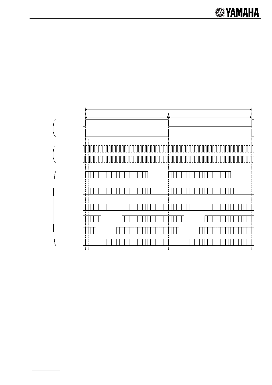
SDO is the demodulated data output of DAIF signal. The data is always 24 bit wide including auxiliary bits.
The timing of serial data interface signal can be selected from the following formats by setting a control
register.
SDBCK
SDWCK
M
L
M
L
M
L
M
L
M
8 7
L
M
8 7
L
M
6 5
L
M
6 5
L
M
4 3
L
M
4
L
3
M
L
M
L
M : MSB DATA L : LSB DATA
1 Frame
L ch
R ch
SDO
SDOFMT1-0 = 00
SDOBIT1-0 = XX
SDOFMT1-0 = 10
SDOBIT1-0 = XX
SDOFMT1-0 = 01
SDOBIT1-0 = 00
SDOFMT1-0 = 01
SDOBIT1-0 = 01
SDOFMT1-0 = 01
SDOBIT1-0 = 10
SDOFMT1-0 = 01
SDOBIT1-0 = 11
SDOBP = 1
SDOBP = 0
SDOWP = 0
SDOWP = 1
Register

YSD917
6
6.
Output terminals for channel status and others:
BS, V, U, C
The signals obtained from DAIF signal including block start, validity flag, user data and channel status are
outputted through BS, V, U and C terminals respectively.
7.
Status information monitor terminals:
/LOCK, ERR, DBL, INT
/LOCK outputs "L" when PLL is locked to DDIN input.
ERR terminal outputs "H" when PLL is not locked to DDIN input or if a parity error is detected.
DBL outputs "H" when PLL is locked at double rate (fs = 64 to 96 kHz) and when this device is not in free-
run mode. It outputs "L" when PLL is locked at normal rate (fs = 32 to 48 kHz) or when this device is in free-
run mode.
INT outputs "H" when the cause of an interrupt is detected.
8.
Serial microcomputer interface:
/CS, SCK, SI, SO
This is a four wire serial interface for reading or writing the control registers.
SO becomes an output terminal only when all of the following conditions are met.
/CS = L
When reading the valid addresses
Timing of 8 bits data output
If any of the above condition is not met, SO outputs High-Z. Thus SO, SI and SCK can be used jointly
with other devices that has the similar interface.
The microcomputer interface functions at all times including power down mode.
9.
Other terminals:
M/S, TEST
M/S selects the master or slave mode when two or more of this LSI are used.
When this terminal is open or connected with VDD, this device operates in master mode, or in slave mode
when connected with VSS.
TEST is a terminal for testing the LSI. Keep it open when using this device.
A0
A1
A2
A3
A4
A5
A6 R/W D0
D1
D2
D3
D4
D5
D6
D7
Don't Care
High-Z
A0
A1
A2
A3
A4
A5
A6 R/W
Don't Care
Don't Care
High-Z
D0
D1
D2
D3
D4
D5
D6
D7
High-Z
SO
SI
SO
SCK
SI
/CS
write
R/W = L
Read
R/W = H
Don't Care
Don't Care
Address of register
Address of register
Read data
Write data
YSD917
7
Electrical Characteristics
1. Absolute maximum ratings
Item Symbol
Conditions
Min.
Max.
Unit
Supply voltage
V
DD
AV
DD
V
ss
-0.5 V
ss
+7.0
V
Input voltage
V
I
-0.5
V
DD
+0.5
V
Storage temperature
T
stg
-50
125
�C
2. Recommended operating conditions
Item Symbol
Conditions
Min.
Typ.
Max.
Unit
Supply voltage
V
DD
AV
DD
4.75
5.0
5.25
V
Operating temperature
XI clock frequency
T
op
f
xin
0
25
24.576
70
�C
MHz
3. DC characteristics
Condition: Under recommended operating conditions
Item Symbol
Conditions
Min.
Typ.
Max.
Unit
H level input voltage (1)
V
IH
1
*1
0.8V
DD
V
H level input voltage (2)
V
IH
2
*2
2.2
V
L level input voltage (1)
V
IL
1
*1
0.2V
DD
V
L level input voltage (2)
V
IL
2
*2
0.8
V
H level output voltage
V
OH
I
OH
= -80
�A
V
DD
-1.0
V
L level output voltage
V
OL
I
OL
= 1.6 mA
0.4
V
Input leakage current
I
LI
Terminal without
pull up resistor
-10 10
�A
Pull up resistor
R
U
25
100
k
Power consumption
P
D
Locked at 96kHz.
120
150
mW
*1 : Applies to input terminals of XI, DDIN, /IC and M/S.
*2 : Applies to input terminals other than the above.

YSD917
8
Example of System Configuration
YSD917
(DIR5)
ADC
DSP
DAC
XI
XO
DAIF
(SPDIF)
DDIN
SDO
SDMCK
SDBCK
SDWCK
Analog
HOST
PROCESSOR
/CS
SCK
SI
SO
/LOCK
ERR
DBL
INT
24.576MHz
YSD917
9
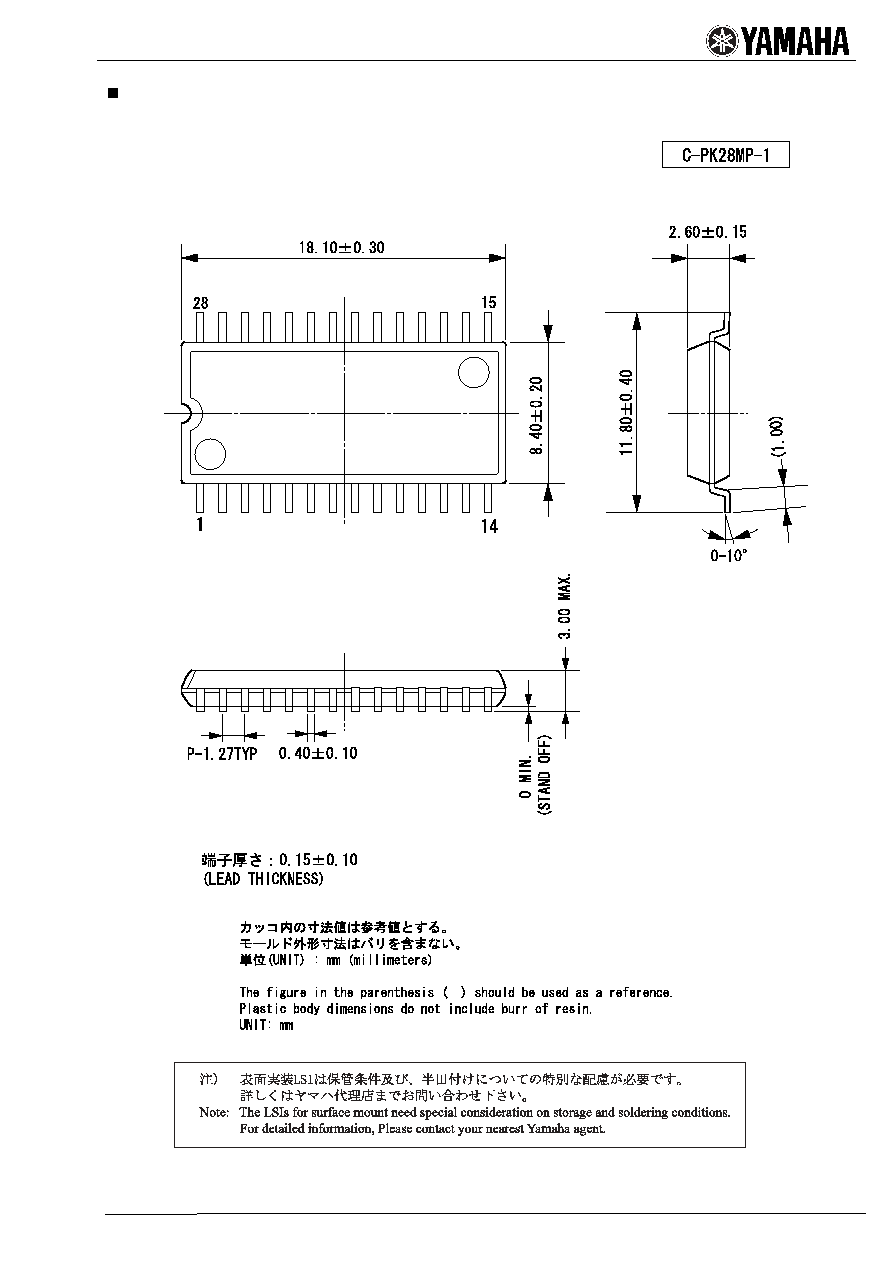
External Dimensions of Package

YSD917
AGENCY
All rights reserved
Address inquiries to:
Semiconductor Sales & Marketing Department
Head Office
203, Matsunokijima, Toyooka-mura
Iwata-gun, Shizuoka-ken, 438-0192, Japan
Tel. +81-539-62-4918
Fax. +81-539-62-5054
Tokyo Office
2-17-11, Takanawa, Minato-ku,
Tokyo, 108-8568, Japan
Tel. +81-3-5488-5431
Fax. +81-3-5488-5088
Osaka Office
3-12-12, Minami Senba, Chuo-ku,
Osaka City, Osaka, 542-0081, Japan
Tel. +81-6-6252-6221
Fax. +81-6-6252-6229
Printed in Japan
2003
IMPORTANT NOTICE
1. Yamaha reserves the right to make changes to its Products and to this document
without notice. The information contained in this document has been carefully checked
and is believed to be reliable. However, Yamaha assumes no responsibilities for
inaccuracies and makes no commitment to update or to keep current the information
contained in this document.
2. These Yamaha Products are designed only for commercial and normal industrial
applications, and are not suitable for other uses, such as medical life support equipment,
nuclear facilities, critical care equipment or any other application the failure of which
could lead to death, personal injury or environmental or property damage. Use of the
Products in any such application is at the customer's sole risk and expense.
3. YAMAHA ASSUMES NO LIABILITY FOR INCIDENTAL, CONSEQUENTIAL, OR
SPECIAL DAMAGES OR INJURY THAT MAY RESULT FROM MISAPPLICATION OR
IMPROPER USE OR OPERATION OF THE PRODUCTS.
4. YAMAHA MAKES NO WARRANTY OR REPRESENTATION THAT THE PRODUCTS
ARE SUBJECT TO INTELLECTUAL PROPERTY LICENSE FROM YAMAHA OR ANY
THIRD PARTY, AND YAMAHA MAKES NO WARRANTY OR REPRESENTATION OF
NON-INFRANGIMENT WITH RESPECT TO THE PRODUCTS. YAMAHA SPECIALLY
EXCLUDES ANY LIABILITY TO THE CUSTOMER OR ANY THIRD PARTY ARISING
FROM OR RELATED TO THE PRODUCTS' INFRINGEMENT OF ANY THIRD
PARTY'S INTELLECTUAL PROPERTY RIGHTS, INCLUDING THE PATENT,
COPYRIGHT, TRADEMARK OR TRADE SECRET RIGHTS OF ANY THIRD PARTY.
5. EXAMPLES OF USE DESCRIBED HEREIN ARE MERELY TO INDICATE THE
CHARACTERISTICS AND PERFORMANCE OF YAMAHA PRODUCTS. YAMAHA
ASSUMES NO RESPONSIBILITY FOR ANY INTELLECTUAL PROPERTY CLAIMS OR
OTHER PROBLEMS THAT MAY RESULT FROM APPLICATIONS BASED ON THE
EXAMPLES DESCRIBED HEREIN. YAMAHA MAKES NO WARRANTY WITH
RESPECT TO THE PRODUCTS, EXPRESS OR IMPLIED, INCLUDING, BUT NOT
LIMITED TO THE WARRANTIES OF MERCHANTABILITY, FITNESS FOR A
PARTICULAR USE AND TITLE.
The specifications of this product are subject to improvement changes without prior notice.
Notice