 | –≠–ª–µ–∫—Ç—Ä–æ–Ω–Ω—ã–π –∫–æ–º–ø–æ–Ω–µ–Ω—Ç: YTD439 | –°–∫–∞—á–∞—Ç—å:  PDF PDF  ZIP ZIP |

YTD439
ISTU
ISDN BRI controller for Terminal Equipment with built-in DSU
YTD439 CATALOG
CATALOG No.:4TD439A2
2001.1
Abstract
YTD439 is a LSI that integrates in a single chip all the communication functions that are
necessary for constructing an ISDN terminal with a built-in DSU. The functions of both the DSU
(U reference point) and terminal (S/T reference point) are packed into the 100-pin SQFP chip
allowing miniaturization of the terminal equipment.
YTD439 has a built-in TD switch function that is necessary for controlling the connection of the
B-channel data. By connecting an external CPU, memory, and CODEC, a terminal with a built-in
DSU can be configured. In addition, YTD439 has a function that reduces the power consumption
by stopping the functions of unused blocks. This is effective for battery-driven terminals.
Features
DSU block
∑ Conforms to TTC Standards JT-I430 and JT-G961.
∑ LT (line termination) function and CT (circuit termination) function.
∑ DSU can be disconnected.
S/T reference point driver/receiver block
∑ Transition to the sleep state possible by setting an I/O register.
CPU interface block
∑ 8-bit or 16-bit data bus selectable.
∑ I/O access through registers.

- 2 -
Layer 1 control block
∑ Frame assembling and disassembling function.
∑ I430 TTL output pin
Layer 2 control block
∑ Built-in LAPD protocol (supports four links).
∑ Call control and D-channel packet function.
Layer 3 interface block
∑ Message exchange through I/O access (large 1088-byte FIFO).
B channel HDLC controller
∑ Supports CRC-CCITT and CRC-32.
∑ 128k/64k/56k rate adaption
B channel transparent
∑ Supports PIAFS 64k/32k.
∑ Flexible rate adaption function.
B channel DATA FIFO
∑ Transmission and reception: 128-byte FIFO
◊
2 channels.
TD switch
∑ Switch circuit for 8 channels of B channel data.
∑ 512 k to 2,048 kHz PCM highway.
Others
∑ Terminal block can be disconnected. Power can be cut off.
∑ Terminal block sleep mode.
∑ Power supply to the analog block: +5 V.
Power supply to the digital block: +5 V or 3.3 V.
∑ 5 V tolerant I/O pin
∑ 100-pin SQFP.
Applications
∑ Terminal adapter
∑ Remote router
∑ ISDN telephone
∑ ISDN home telephone
∑ ISDN Facsimile
- 3 -
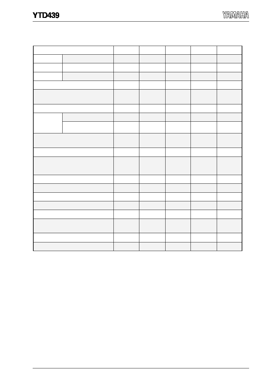
Functional Comparison of YAMAHA ISDN LSIs
Note 1: DMA transfer: Request function only
I/O transfer:
4-byte FIFO
Note 2: Digital power supply only
External
[YTD421]
External
DMA Transfer
or
I/O Transfer
I/O Transfer
DMA Transfer
or
I/O Transfer
DMA Transfer
or
I/O Transfer
I/O Transfer
DMA Transfer
or
I/O Transfer
(Note 1)
+5
or
+3.3 (Note 2)
+5
or
+3.3 (Note 2)
+5
or
+3.3 (Note 2)
2
2
(2)
2
(2)
2
2
2
+5
+5
32, 56, 64
32, 56, 64
1997 edition
1993 edition
1997 edition
1997 edition
1993 edition
1998 edition
1993 edition
1998 edition
1993 edition
1993 edition
1993 edition
100-pin SQFP 100-pin SQFP 100-pin SQFP
100-pin SQFP
20-pin SSOP
Function
YTD428
YTD421
ETSI
ETS 300 012, ETS 300 125
North American Switches
National ISDN-1/2, AT&T 5ESS,
Nortel DMS-100
DSU Function
S/T Ref. Point Analog Driver/Receiver
D Channel Layer 3 Data Transfer Method
TTC Standard
TTC Standard
JT-I430
JT-Q920
JT-Q921
Layer 1
Layer 2
YTD423
YTD436
YTD439
1997 edition
TTC Standard
JT-G961
B Channel Data Transfer Method
B Channel Internal Clock Mode (kHz)
HDLC Controller for B Channel Data
B Channel External Clock Mode
TD Switch
Clock Output Function for CPU
Signal Output Function for Testing
5-V Tolerant I/O pin
Package
Power Supply (V)
Circuit switching
Dch Packet Switching
(Teleaction communication)
Maximum D
Channel Links

- 4 -
Block Diagram
User-Network Interface Block Diagram
YTD439 is best-suited for applications in terminal equipment with built-in DSU (TA, TE1)
such as terminal adapters and remote routers with built-in DSUs.
YTD439 contains a DSU function, which is necessary between the ISDN switch and the user-
network interface, and layer 1 and layer 2 functions, which are required of ISDN system
equipment. By adding minimal peripheral parts such as microprocessor and CODEC, terminal
equipment can be optimally configured.
ISDN
Network
YTD436 or
YTD423 + YTD421
YTD439
User's premises
TE1
(ISDN terminal)
NT2
(PBX, etc.)
NT1
(DSU)
TE2
(Non-ISDN
terminal)
TE2
TA
(Terminal adapter)
TE1
TE1
TA with
built-in DSU
T
S/T
R
U
R
S
S
U
S/T
YTD428 (DSU)
TE2
TE1
TA with
built-in DSU
R
S/T

- 5 -
Internal Block Diagram
Rate adaption
block
Transparent
PIAFS
FIFO
(1088 byte)
HDLC
controller
64k
◊
2
16k
B channel
data
FIFO
(128 byte
◊
2)
Control
I/O register
Layer 1
control
block
Terminal
block
Layer 2 control
block
(LAPD)
Circuit
termination
block
Line
termination
block
U ref.
point I/F
Layer 3 I/F block
T ref.
point
connection
control
block
DSU block
B channel data control block (CH-A)
B channel connection section
TD switch (8ch)
B channel data control block (CH-B)
Internal bus
B channel PCM highway I/F (CODEC, etc)
(512 k to 2,048 kHz )
U ref. point
15.36 MHz
S/T ref.
point
CPU I/F
Programmable I/O
S/T ref.
point
driver/
receiver
block
Clock
generator
D channel
B1/B2
channel