ACE9020 is a VHF oscillator, up-converter and prescaler.
It is used in an offset modulated transmit architecture where a
UHF synthesiser makes the channel selection and a second
synthesiser generates a fixed transmit offset.
A VCO signal drives a buffer in ACE9020 to feed an on-
chip prescaler and transmit up-converter. The prescaler is a
dual two-modulus divider and drives the main synthesiser
input of the ACE9030. The SSB up-converter suppresses the
unwanted transmit sideband.
The VHF oscillator is buffered to drive the auxiliary
synthesiser input of the ACE9030 and is locked to the offset
frequency. This frequency is modulated by varying the
resonant frequency of the external tank circuit. Both this
oscillator and the UHF VCO drive the up-converting mixer to
generate the transmit signal.
Various power saving modes for battery economy are
included. These allow the transmit sections to be shut down
during stand-by and the whole chip can be shut down during
sleep mode. The circuit techniques used have been chosen to
minimise external components and at the same time give very
high performance.
Features
∑
Low Power Low Voltage (3.6 to 5.0 V) Operation
∑
Power Down Modes
∑
Differential Signals to Minimise Cross-talk
∑
Auxiliary Oscillator with Transmit Up-converter
∑
Prescaler for Main Synthesiser
∑
Part of the ACE Integrated Cellular Phone Chipset
∑
Small Outline 28 pin Package
Applications
∑
AMPS and TACS Cellular Telephone
∑
Two-Way Radio Systems
Related Products
ACE9020 is part of the following chipset:
∑
ACE9030 Radio Interface and Twin Synthesiser
∑
ACE9040 Audio Processor
∑
ACE9050 System Controller and Data Modem
ABSOLUTE MAXIMUM RATINGS
Supply voltage 6V
Storage temperature - 65
∞C to + 150∞C
Operating temperature - 30
∞C to + 85∞C
Voltage at any pin
-0.3V to V
CC
+0.3V
Static Sensitivity (HBM) min
500V
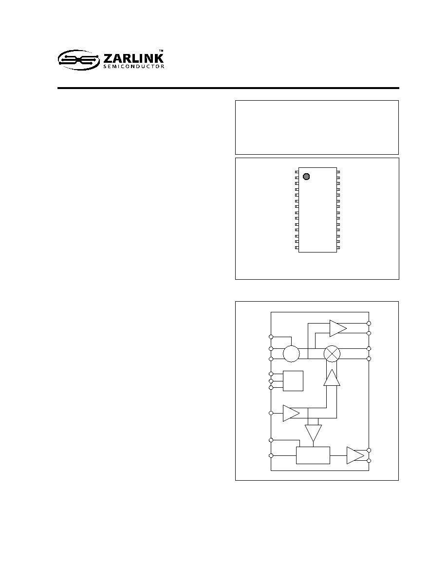
Figure 2 - ACE9020 simplified block digram
ACE9020
Receiver and Transmitter Interface
DS4287
ISSUE 5.0
December 1997
Ordering Information
SSOP 28 lead package, code NP28
ACE9020B/KG/NP1S - anti-static sticks
ACE9020B/KG/NP1T - tape mounted
Figure 1 - Pin connections - top view
PD1
PD2
GND
BIAS_REF
VCC_TX
TXPA+
TXPA-
RSET_TXPA
GND_TXOSC
TANK+
TANK-
VCC_DIV
GND_OSC
MOD_CNTRL
DIV_OUT+
DIV_OUT-
RATIO_SEL
GND_DIV
TXOSC+
TXOSC-
VCC_TXOSC
GND_RX
RXVCOIN
n.c.
VCC_RX
n.c.
n.c.
VCC
1
28
14
15
Note: Pin 1 is identified by moulded spot
and by coding orientation.
NP28
ACE9020
VHF
OSC
RSET_TXPA
TANK+
TANK-
TXOSC+
TXOSC-
TXPA+
TXPA-
BIAS &
POWER
DOWN
CONTROL
BIAS_REF
PD1
PD2
RXVCOIN
DIV_OUT+
DIV_OUT-
RATIO_SEL
MOD_CNTRL
DIVIDE BY
64/65 OR 128/129

2
ACE9020
Pin No.
Name
Type
Description
1
PD1
I
Power down control input 1
2
PD2
I
Power down control input 2
3
GND
Supply
Ground
4
BIAS_REF
I
Reference current for bias control
5
VCC_TX
Supply
Transmit section supply voltage
6
TXPA+
O
Transmit up-converter open collector output
7
TXPA-
O
Transmit up-converter open collector output
8
RSET_TXPA
I
Reference current for transmit oscillator
9
GND_TXOSC
Supply
Ground
10
TANK+
I
Transmit oscillator tank circuit
11
TANK-
I
Transmit oscillator tank circuit
12
VCC_DIV
Supply
Divider section supply voltage
13
GND_OSC
Supply
Ground
14
MOD_CNTRL
I
Modulus control input
15
DIV_OUT+
O
Divider output positive
16
DIV_OUT-
O
Divider output negative
17
RATIO_SEL
I
Ratio select
18
GND_DIV
Supply
Ground divider section
19
TXOSC+
O
Transmit oscillator monitor output positive
20
TXOSC-
O
Transmit oscillator monitor output negative
21
VCC_TXOSC
Supply
Transmit oscillator supply voltage
22
GND_RX
Supply
Ground
23
RXVCOIN
I
Input buffer for 1GHz VCO signal from ACE9010
24
n.c.
-
No connection
25
VCC_RX
Supply
Receiver section supply voltage
26
n.c.
-
No connection
27
n.c.
-
No connection
28
VCC
Supply
ON/OFF logic supply voltage
PIN Connections
Characteristic
Min
Typ
Max
Unit
Supply Currents
Sleep PD1 = 0, PD2 = 0
0.11
mA
Standby PD1 = 1, PD2 = 0
6
8
mA
Transmit Set Up PD1 = 0, PD2 = 1
36
51
mA
Duplex PD1 = 1, PD2 = 1
48
63
mA
Input Levels
PD1, PD2 High
1.9
3.1
V
PD1, PD2 Low
0
0.5
V
Mod Cntrl High
Vcc/2 + 0.3
Vcc
V
Mod Cntrl Low
0
Vcc/2 - 0.3
V
Ratio Sel High
0.6Vcc
Vcc
V
Ratio Sel Low
0
0.4Vcc
V
Input Currents
PD1, PD2 High
40
µA
PD1, PD2 Low
-0.1
0.1
µA
DC Characteristics
Electrical Characteristics
These characteristics apply over these ranges of conditions (unless otherwise stated):
T
AMB
= ≠ 30
∞C to + 85∞C, V
CC
= 3.75
± 0.15V or 4.85 ± 0.15V (see fig. 3 for test circuit).

2
ACE9020
Notes:
1. Exceptions.
Harmonics of divider output -37dBc max applicable when fVCO = 975.1354 MHz Ratio = 65
10th Harmonic of faux -47dBc applicable when faux = 90MHz, fVCO = 989.9375MHz
2. Residual modulation referenced to a 1kHz signal giving 3kHz deviation. Measured with 750
µs de-emphasis and CCITT
filter.
Characteristic
Min
Typ
Max
Unit
TXOSC Output
Differential Output
500
mV p-p
TxOsc Frequency
70
140
MHz
Frequency / Supply Sensitivity
75
kHz
Spurii > 700MHz
-40
dBc
Differential Output Capacitance
2
pF
External Tank Inductance f = 90MHz
82
100
nH
External Tank Inductance f = 122.5MHz
56
68
nH
Power up time (from standby)
65
µs
TXPA Output Signal
Output Power (RL = 50
)
0
3
6
dBm
Noise at
f = +/- 45 MHz
-145
dBc/Hz
Noise at
f = +/- 25 kHz
-100
dBc/Hz
Harmonic Content
-20
dBc
Spurious - Image
-10
dBc
Spurious (fVCO
± 2faux)
-30
dBc
Spurious (fVCO
± 3faux)
-25
dBc
Spurious (
f = 45MHz ± 15 kHz) except 2fVCO - 9faux
-105
dBc
Spurious 2fVCO - 9faux
-60
dBc
Spurii within 800 to 940 MHz (note1)
-70
dBc
Other Spurii except image
-30
dBc
Isolation TXPA off (PD2 = PD1 = 1)
55
dB
Power up time
25
µs
Isolation TXPA to RVCOIN
45
dB
Residual Modulation (note 2)
-40
dB
RVCOIN Input Signal
Signal Level
-10
dBm
Input Impedance
50
Divider input frequency
800
1100
MHz
Upconverter input frequency
910
1040
MHz
Phase Noise
f = 45MHz
-155
dBc/Hz
Phase Noise
f = 25kHz
-117
dBc/Hz
Spurious - harmonic
-20
dBc
Spurious - non-harmonic
-80
dBc
Divider
Differential Output Level
500
600
mV p-p
Output Rise / Fall time
15
ns
Mod Control Set up time
20
ns
Mod Control Hold time
1
ns
AC Characteristics
Electrical Characteristics
These characteristics apply over these ranges of conditions (unless otherwise stated):
T
AMB
= -30
∞C to + 85∞C, V
CC
= 3.75
± 0.15V or V
CC
4.85
± 0.15V (see fig. 3 for test circuit).
4
ACE9020
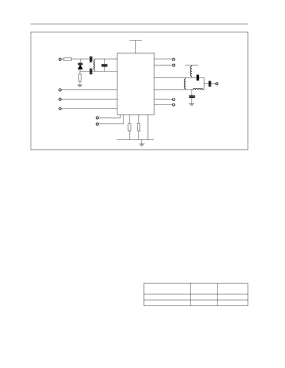
Figure 3 - ACE9020 Test circuit
Description
The ACE9020 is designed for use in a transceiver such as
an analog cellular phone, which uses an offset modulation
transmit architecture. The circuit consists of a VHF voltage
controlled oscillator to generate the offset frequency, an
upconverter to transmit frequency and also a prescaler for the
main UHF phase locked loop. The Rxvcoin signal to the
ACE9020 is normally the UHF local oscillator used for
downconversion.
A basic block diagram is shown in fig. 2, further
information on external connections is provided in the test
circuit (fig. 3) and the applications diagram (fig. 4).
VHF Oscillator
This oscillator is a differential design which uses an
external tank circuit as shown in fig. 3 and fig. 4. The
components shown in fig. 3 give a VCO frequency of 90MHz.
A varactor diode is coupled capacitively to the tank circuit; the
anode is referenced to ground via a resistor. The VCO control
from a synthesiser (eg ACE9030) charge pump output is
applied to the cathode of the varactor also through a resistor.
These resistors should be the same value to keep the
differential circuit balanced. The VCO gain with the
components shown will be typically 2 MHz/V. Modulation is
applied to the anode via a resistive divider as shown in fig. 4;
the actual signal applied to the varactor will be small as the
frequency deviation will typically be a maximum of 12kHz in
many applications. Differential buffered outputs from the
oscillator (TXOSC) interface directly to the ACE9030 auxiliary
synthesier inputs.
Upconverter
An image reject mixer is used for the upconversion. This
provides typically 20dB rejection of the unwanted upper
sideband. The quadrature networks for the mixer are all
provided on chip; this is optimised for UHF local oscillator and
VHF offset oscillator frequencies typically used for analog
cellular phones on the AMPS and TACS systems. Further
filtering of the TXPA output will be required to provide further
suppression of the unwanted upper sideband, local oscillator
signal and harmonics to meet cellular telephone
specifications. SAW filters are available for the various
transmit frequency bands.
The upconverter outputs (TXPA + and -) are differential
current outputs. The use of differential outputs minimises
current switching within the device and thus minimise cross-
talk to other circuit blocks. The TXPA outputs must be
matched to the external filter, normally 50
and single-ended.
The network shown in fig. 3 provides a transformation from
400
differential to 50 single-ended and also provides dc
bias from the Vcc supply to the open collector TXPA outputs.
This network provides plus and minus 90
∞ phase shift in each
output which are then summed. Alternatively a Balun
transformer could be used, it will again be necessary to
provide dc bias to the TXPA outputs. The load to the current
outputs should be maximised to obtain the maximum power
output; 400
is an optimum figure as higher values require
impractical component values for matching.
Prescaler
The two modulus prescaler is part of the UHF phase
locked loop. It will typically be operating with ACE9030 radio
interface and synthesiser. There is also a choice of divider
ratio, set by the ratio select input as shown in table. 1, below.
The differential divider outputs can be directly coupled to
the ACE9030 main synthesiser inputs.
ACE9020
Rxvcoin
22k
18k
Vcc
Vcc
VCO Control
TXOsc
Div Out
+
-
+
-
+
TXPA
-
27n
27n
18n
1p
27p
1p
Tx
Output
100p
100p
18p
100n
BB545
6k8
6k8
5,12,21,25,28
10
11
23
4
8
3,9,13,
18,22
16
15
19
20
6
7
Mod Cntrl
Ratio Sel
14
17
PD1
1
2
PD2
faux = 90 MHz
Ratio Sel
Ratio Sel
= LOW
= HIGH
Mod_Cntrl = LOW
˜129
˜65
Mod_Cntrl = HIGH
˜128
˜64
Table 1

4
ACE9020
Power Control Circuits
The inputs PD1 and PD2 are used to select the operating
modes as shown below:
PD1
PD2
Mode
0
0
Sleep
All circuits off
1
0
Standby
Prescaler On
1
1
Transmit Set Up
Prescaler, VHF
oscillator on. Upconverter off
0
1
Duplex
All circuits on
The power down inputs (PD1, PD2) are compatible with
ACE9030 digital outputs (DO5, 6, 7). These modes allow
circuit operation and power consumption to be optimised. The
ACE9020 can be put in sleep mode (0, 0) when the power
consumption is minimal. The standby mode (1, 0) is used
when the phone is in standby (receive only). The prescaler is
operational to maintain the main UHF PLL; all circuitry
associated with transmit functions is turned off.
There is an intermediate transmit set up state (1, 1). This
allows the VHF oscillator and phase locked loop to stabilise
before enabling the upconverter, preventing spurious
transmissions. The time required for this state will be
determined primarily by the VHF PLL settling time. The power
down inputs can then be set to (0, 1) the full duplex condition.
The intermediate state should also be used during a `handoff'
during conversation on an analogue cellular phone, the VHF
PLL continuing to operate while the main UHF PLL changes
channel, the transmit output being disabled. It is also
recommended that the intermediate state is used when going
from duplex (0, 1) to standby (1, 0) modes.
Operating Notes
Good RF layout techniques should be used for this device
to obtain optimum performance and also minimise crosstalk
between circuit blocks. RF supply decoupling should be
provided adjacent to Vcc pins; a value of 27pF is
recommended.
Two external bias resistors are required. A 22k
resistor
is connected from BIAS REF (Pin 4) to ground. This sets an
accurate reference current for the chip. An 18k resistor is
connected from RSET TXPA (Pin 8) to ground which controls
the output level of the VHF oscillator and hence the TXPA
output level.
Figure 4 - Application Diagram

www.zarlink.com
Information relating to products and services furnished herein by Zarlink Semiconductor Inc. trading as Zarlink Semiconductor or its subsidiaries (collectively
"Zarlink") is believed to be reliable. However, Zarlink assumes no liability for errors that may appear in this publication, or for liability otherwise arising from the
application or use of any such information, product or service or for any infringement of patents or other intellectual property rights owned by third parties which may
result from such application or use. Neither the supply of such information or purchase of product or service conveys any license, either express or implied, under
patents or other intellectual property rights owned by Zarlink or licensed from third parties by Zarlink, whatsoever. Purchasers of products are also hereby notified
that the use of product in certain ways or in combination with Zarlink, or non-Zarlink furnished goods or services may infringe patents or other intellectual property
rights owned by Zarlink.
This publication is issued to provide information only and (unless agreed by Zarlink in writing) may not be used, applied or reproduced for any purpose nor form part
of any order or contract nor to be regarded as a representation relating to the products or services concerned. The products, their specifications, services and other
information appearing in this publication are subject to change by Zarlink without notice. No warranty or guarantee express or implied is made regarding the
capability, performance or suitability of any product or service. Information concerning possible methods of use is provided as a guide only and does not constitute
any guarantee that such methods of use will be satisfactory in a specific piece of equipment. It is the user's responsibility to fully determine the performance and
suitability of any equipment using such information and to ensure that any publication or data used is up to date and has not been superseded. Manufacturing does
not necessarily include testing of all functions or parameters. These products are not suitable for use in any medical products whose failure to perform may result in
significant injury or death to the user. All products and materials are sold and services provided subject to Zarlink's conditions of sale which are available on request.
Purchase of Zarlink's I
2
C components conveys a licence under the Philips I
2
C Patent rights to use these components in an I
2
C System, provided that the system
conforms to the I
2
C Standard Specification as defined by Philips.
Zarlink, ZL and the Zarlink Semiconductor logo are trademarks of Zarlink Semiconductor Inc.
Copyright 2003, Zarlink Semiconductor Inc. All Rights Reserved.
TECHNICAL DOCUMENTATION - NOT FOR RESALE
For more information about all Zarlink products
visit our Web Site at