Ordering Information
Industrial temperature range
TQFP 64 lead 10 x 10 mm, 0∑5 mm pitch
ACE9030M/IW/FP1N - shipped in trays and dry packed
ACE9030M/IW/FP1Q - tape & reel and dry packed
TQFP 64 lead 7 x 7 mm, 0∑4 mm pitch
ACE9030M/IW/FP2N - shipped in trays and dry packed
ACE9030M/IW/FP2Q - tape & reel and dry packed
ACE9030 is a combined radio interface circuit and twin
synthesiser, intended for use in a cellular telephone.
The radio interface section contains circuits to monitor
and control levels such as transmit power in the telephone,
circuits to demodulate the frequency modulated signal to
audio, and a crystal oscillator with a frequency multiplier.
The Main synthesiser has normal and fractional-N modes
both with optional speed-up to select the desired channel. The
Auxiliary synthesiser is used for the transmit-receive offset
and for modulation.
Both sections are controlled by a serial bus and have
software selected power saving modes for battery economy.
The circuit techniques used have been chosen to minimise
external components and at the same time give very high
performance.
Features
∑
Low Power Low Voltage (3∑6 to 5∑0 V) Operation
∑
Serial Bus Controlled Power Down Modes
∑
Simple Programming Format
∑
Reference Crystal Oscillator
∑
Frequency Multiplier for LO2 Signal
∑
8∑064 MHz Output for External Microcontroller
∑
Main Synthesiser with Fractional-N Option
∑
Auxiliary Synthesiser
∑
Main Synthesiser Speed-up Options
∑
FM Discriminator for 450 kHz or 455 kHz I.F. Signal
∑
Radio System Control Interface
∑
Part of the ACE Integrated Cellular Phone Chipset
∑
TQFP 64 pin 0∑4 mm and 0∑5 mm pitch packages
Related Products
ACE9030 is part of the following chipset:
∑
ACE9020 Receiver and Transmitter Interface
∑
ACE9040 Audio Processor
∑
ACE9050 System Controller and Data Modem
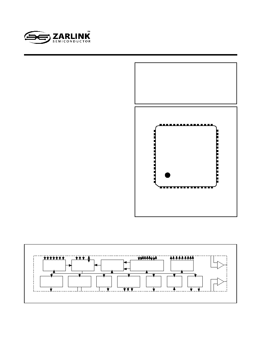
Figure 1 - Pin connections - top view
Applications
∑
AMPS and TACS Cellular Telephone
∑
Two-way Radio Systems
Figure 2 - ACE9030 Simplified Block Diagram
POLLING
ADC
BUS
INTERFACE
LOCK
DETECT
TWIN
SYNTHESISER
DIGITAL
OUTPUTS
CRYSTAL
MULTIPLIER
CRYSTAL
OSCILLATOR
8 MHz
PLL
TRIMMING
DACs
AFC
MIXER
AMP &
LIMITER
AUDIO
DEMOD.
-
+
-
+
L.F. AMPS
ACE9030
Radio Interface and Twin Synthesiser
Preliminary Information
DS4288
ISSUE 2.0
January 1998
VP64
FP64
Note: Pin 1 is identified by moulded spot
and by coding orientation
DOUT5
DOUT6
DOUT7
FIAB
FIA
VDDSA
VSSSA
FIMB
FIM
VSSD
PDI
PDP
RSMA
DECOUP
RSC
VDDD
DOUT0
VDDX
DOUT1
VDDA
VSSA
LO2
ADC1
ADC3A
ADC3B
ADC5
DOUT8
DAC2
DAC1
DOUT2
CIN1
CIN2
MODMP
MODMIN
TEST
PDA
VDDSUB
DOUT3
DOUT4
AMPP2
AMPN2
DAC3
AMPP1
AMPN1
AMP01
ADC2A
ADC2B
ADC4
AMP02
RXCD
LA
TCHC
LA
TCHB
D
ATA
CL
AFCOUT
AUDIO
BP
AFCIN
IREF
VSSL
VDDL
CLK8
C8B
VDDSUB2
ACE9030
2
ACE9030
Figure 3 - ACE9030 Block diagram
+
-
+
-
+
-
+
-
MAIN SYNTHESISER
with FRACTIONAL-N
SERIAL
BUS INPUT
REGISTERS (SYTHS)
SERIAL BUS I/O TO
RADIO INTERFACE
BAND-GAP
REFERENCE
LOCK
DETECT
AUXILIARY
SYNTHESISER
REFERENCE
DIVIDER
FILTER
DEFINE
LEVELS
DATA &
CONTROL
DEMOD
MIXER
TEST
SEL.
MULT
x3, x5
VDDL
VSSL
SWITCHES
ADC1
XO
INPUT
SCANNER
8 Bit
A
to D Converter
DEMUL
TIPLEXER
REGISTERS
SELECT
OR
VREF
RXCD
VDDX
DOUT0
DOUT1
DOUT2
DOUT3
DOUT4
DOUT5
DOUT6
DOUT8
AUDIO
BP
AFCOUT
DAC1
DAC2
VSSD
VDDD
MODMN
MODMP
PDI
PDP
RSMA
RSC
DAC3
DAC3
DAC2
DAC1
BIAS
GEN.
PDA
DOUT7
AMPO2
AMPO1
VSSL
VDDL
IREF
VSSA
VDDA
LEVEL SENSE
AMPP1
OSC8
PLL.
AMPN1
AMPP2
ADC2A
AMPN2
ADC1
ADC2B
ADC3A
ADC4
ADC5
ADC3B
CRYSTAL
OSC.
AFCIN
C8B
CLK8
LO2
CIN2
CIN1
LATCHB
VDDSUB2
VDDSUB
DECOUP
VDDSA
VSSSA
FIM
FIMB
CL
DATA
LATCHC
TEST
FIA
FIAB

2
ACE9030
PIN Descriptions
The relevant supplies (V
DD
) and grounds (V
SS
) for each circuit function are listed. All V
DD
and V
SS
pins should be used.
Pin No.
Name
Description
VDD
VSS
1
AMPO2
LF amplifier 2 output.
VDDA
VSSA
2
RXCD
Receive carrier detect (ADC1 comparator) output.
VDDL
VSSL
3
LATCHC
Synthesiser programme enable input.
VDDL
VSSL
4
LATCHB
Radio interface programme enable input.
VDDL
VSSL
5
DATA
Serial data; programming input, results output.
VDDL
VSSL
6
CL
Clock input for programming bus and for I.F. sampling.
VDDL
VSSL
7
AFCOUT
Output from AFC amplifier after sampling.
VDDL
VSSL
8
AUDIO
Output from f.m. discriminator after filtering.
VDDA
VSSA
9
BP
Feedback input to audio bandpass filter.
VDDA
VSSA
10
AFCIN
Input to AFC amplifier and f.m. discriminator.
VDDL
VSSL
11
IREF
Bias current input for radio interface, connect setting resistor to ground.
≠
VSSA
12
VSSL
Ground for radio interface logic.
≠
≠
13
VDDL
Power supply to radio interface logic.
≠
≠
14
CLK8
Output clock at 8∑064 MHz, locked to crystal.
VDDL
VSSL
15
C8B
8∑064 MHz oscillator charge pump output and control voltage input.
VDDA
VSSA
16
VDDSUB2
Second connection for clean positive supply to bias substrate.
VDDA
VSSA
17
CIN2
Connection for crystal oscillator.
VDDL
VSSL
18
CIN1
Connection for crystal oscillator.
VDDL
VSSL
19
DOUT2
Digital control output 2.
VDDL
VSSL
20
DAC1
Analog control output 1.
VDDA
VSSA
21
DAC2
Analog control output 2.
VDDA
VSSA
22
DOUT8
Digital control output 8.
VDDA
VSSA
23
ADC5
Analog to digital converter input 5.
VDDA
VSSA
24
ADC3B
Analog to digital converter input 3B.
VDDA
VSSA
25
ADC3A
Analog to digital converter input 3A.
VDDA
VSSA
26
ADC1
Analog to digital converter input 1.
VDDA
VSSA
27
LO2
Output from crystal frequency multiplier.
VDDA
VSSA
28
VSSA
Ground for radio interface analog parts.
≠
≠
29
VDDA
Power supply to radio interface analog parts.
≠
≠
30
DOUT1
Digital control output 1.
VDDX
≠
31
VDDX
Power supply to DOUT1 and DOUT2 switches.
≠
≠
32
DOUT0
Digital control output 0.
VDDX
≠
33
VDDD
Power supply to synthesisers, except input buffers and the bandgap.
≠
≠
34
RSC
Fractional-N compensation bias current, resistor to ground.
≠
VSSSA
35
DECOUP
Bandgap reference decoupling capacitor connection.
VDDSA
VSSSA
36
RSMA
Bias current for synthesiser charge pumps, resistor to ground.
≠
VSSSA
37
PDP
Main synthesiser proportional charge pump output.
VDDD
VSSD
38
PDI
Main synthesiser integral charge pump output.
VDDD
VSSD
39
VSSD
Ground for synthesisers, except input buffers and the bandgap.
≠
≠
40
FIM
Main synthesiser positive input from prescaler.
VDDSA
VSSSA
41
FIMB
Main synthesiser negative input from prescaler.
VDDSA
VSSSA
42
VSSSA
Ground for FIM and FIA input buffers and the bandgap.
≠
≠
43
VDDSA
Power for FIM and FIA input buffers and the bandgap.
≠
≠
44
FIA
Auxiliary synthesiser positive input from VCO.
VDDSA
VSSSA
45
FIAB
Auxiliary synthesiser negative input from VCO.
VDDSA
VSSSA
46
DOUT7
Digital control output 7.
VDDD
VSSD
47
DOUT6
Digital control output 6.
VDDD
VSSD
48
DOUT5
Digital control output 5.
VDDD
VSSD
49
MODMP
Modulus control output to prescaler - positive sense.
VDDD
VSSD
50
MODMN
Modulus control output to prescaler - negative sense.
VDDD
VSSD
51
TEST
Test input and output for synthesisers.
VDDD
VSSD
52
PDA
Auxiliary synthesiser charge pump output.
VDDD
VSSD
53
VDDSUB
Clean positive supply to bias substrate.
≠
≠
54
DOUT3
Digital control output 3.
VDDL
VSSL
55
DOUT4
Digital control output 4.
VDDL
VSSL
56
AMPP2
LF amplifier 2 positive input.
VDDA
VSSA
57
AMPN2
LF amplifier 2 negative input.
VDDA
VSSA
58
DAC3
Analog control output 3.
VDDL
VSSL
59
AMPP1
LF amplifier 1 positive input.
VDDA
VSSA
60
AMPN1
LF amplifier 1 negative input.
VDDA
VSSA
61
AMPO1
LF amplifier 1 output.
VDDA
VSSA
62
ADC2A
Analog to digital converter input 2A.
VDDA
VSSA
63
ADC2B
Analog to digital converter input 2B.
VDDA
VSSA
64
ADC4
Analog to digital converter input 4.
VDDA
VSSA
4
ACE9030
Figure 4 - Typical VDD local decoupling networks without series resistors
Figure 5 - Typical VDD local decoupling networks with series resistors
at all times including during power on and off ramping. As the
current taken through these V
DD
's is significantly less than
through the other V
DD
's this requirement can be easily met by
directly connecting all V
DD
pins to a common point on the circuit
board but with the decoupling capacitors distributed to
minimise cross-talk caused by common mode currents. If low
value series resistors are to be included in the V
DD
connec-
tions, with decoupling capacitors by the ACE9030 pins to
further reduce interference, the V
DDSUB
and V
DDSUB2
pins should
not have such a resistor in order to guarantee that their voltage
is not slowed down at power-on. Power switches to DOUT0
and DOUT1 are supplied from V
DDX
and are specified for a total
current of up to 40 mA so any resistor in the V
DDX
connection
must be very low, around 1
, in order to avoid excessive
voltage drop; it is recommended that this supply has no series
resistor. These two methods are shown in circuit diagrams,
figures 4 and 5. In both circuits the main V
DD
must also have
good decoupling.
Main VDD
VDDSUB
VDDSUB2
VDDL
VDDA
VDDX
VDDD
VDDSA
VDDSUB
VDDSUB2
VDDL
VDDA
VDDX
VDDD
VDDSA
Main VDD
No Resistor
No Resistor
Very
Small
Absolute Maximum Ratings
Supply voltage from ground ≠ 0∑3 V to + 6∑0 V
(any V
DD
to any V
SS
)
Supply voltage difference ≠ 0∑3 V to + 0∑3 V
(any V
DD
to any other V
DD
)
Input voltage V
SS
≠ 0∑3 V to V
DD
+ 0∑3 V
(any input pin to its local V
SS
and V
DD
)
Output voltage V
SS
≠ 0∑3 V to V
DD
+ 0∑3 V
(any output pin to its local V
SS
and V
DD
)
Storage temperature ≠ 55
∞C to + 150 ∞C
Operating temperature ≠ 40
∞C to + 85 ∞C
These are not the operating conditions, but are the
absolute limits which if exceeded even momentarily may
cause permanent damage. To ensure sustained correct op-
eration the device should be used within the limits given under
Electrical Characteristics.
To avoid any possibility of latch-up the substrate connec-
tions V
DDSUB
and V
DDSUB2
must be the most positive of all V
DD
's
4
ACE9030
Parameter
Min.
Typ.
Max.
Unit
Conditions
Power supply
Supply current, Radio Interface:
Sleep mode
2.3
2∑7
mA
XO, OSC8 on
Fully operating (excluding I
DDX
)
7
mA
(see Note 1)
Supply current, Synthesisers: V
DD
=5V
f
REF
= 10 MHz
Main and Auxiliary ON
5
mA
f
MAIN
= 10 MHz
Main ON and Auxiliary in Standby
3.7
mA
f
AUX
= 10 MHz
Main in Standby and Auxiliary ON
3
mA
(see Note 2)
Main and Auxiliary in Standby, with Bandgap off
100
µA
Supply current, Synthesisers:
f
REF
= 15 MHz
Main and Auxiliary ON
3
mA
f
MAIN
= 16 MHz
Main ON and Auxiliary in Standby
2
mA
f
AUX
= 90 MHz
Main in Standby and Auxiliary ON
2
mA
(see Note 2)
Main and Auxiliary in Standby
100
µA
Input and output signals
Logic input HIGH (LATCHC, LATCHB, DATA,
CL, and TEST)
0∑7 x V
DD
V
DD
+ 0∑3
V
Logic input LOW (LATCHC, LATCHB, DATA,
CL, and TEST)
≠ 0∑3
+ 0∑8
V
Input capacitance (signal pins)
10
pF
Pin voltage
Input leakage (signal pins)
1
µA
V
SS
to V
DD
Logic output HIGH (RXCD, DATA, AFCOUT,
V
DD
≠ 0∑5
V
TEST and DOUT2, 3 and 4)
External load:
Logic output LOW (RXCD, DATA, AFCOUT,
0∑4
V
20 k
& 30 pF
TEST and DOUT2, 3 and 4)
Output ON level, DOUT0 and DOUT1
V
DDX
≠ 0∑2
V
I
OH
= 20 mA.
Output HIGH level, DOUT5, 6 and 7
2∑3
2∑9
V
I
OH
= 80
µA
Output LOW level, DOUT5, 6 and 7
0∑3
V
I
OL
= 0.2
µA
Trimmed output level ON, DOUT8
3∑35
3∑55
V
I
OH
= 135 to 400
µA.
Level difference, DOUT8 ON ≠ ADC reference
≠ 5
+ 15
mV
Output level OFF, DOUT8
0.4
V
MODMP, MODMN output HIGH
V
DD
/2 + 0∑35
V
DD
/2 + 1∑0
V
I
OH
= 10
µA
MODMP, MODMN output LOW
V
DD
/2 ≠ 1∑0
V
DD
/2 ≠ 0∑35
V
I
OL
= ≠ 10
µA
Input Schmitt Hysteresis, pins CL, LATCHB,
0∑3
V
LATCHC, DATA.
Analog circuits bias resistor on I
REF
68
k
V
DD
@ 3∑75 V
100
k
V
DD
@ 4∑85 V
Electrical Characteristics
These characteristics apply over these ranges of conditions (unless otherwise stated):
T
AMB
= ≠ 40
∞C to + 85 ∞C, V
DD
= + 3∑6 to + 5∑0 V, GND ref. = V
SS
D.C. Characteristics
Notes
1. The sleep current is specified with the crystal oscillator (XO) and the OSC8 oscillator and PLL running as these are normally needed to provide
the clock to the system controller.
2. The terms f
REF
, f
MAIN
, and f
AUX
refer to the frequencies of the Reference inputs (Crystal oscillator, pins CIN1 and CIN2), the Main synthesiser
inputs (pins FIM and FIMB) and the Auxiliary synthesiser inputs (pins FIA and FIAB) respectively.