DS3605-2.2
The GP1020 is a six-channel CMOS digital correlator which
has been designed to work with the GP1010 L1-channel down-
converter or other integrated circuits, and may be used to acquire
and track the GPS C/A code or the GLONASS signals.
For each of the six channels the GP1020 includes independ-
ent digital down-conversion to baseband, C/A code generation,
correlation, and accumulate-and-dump registers.
The GP1020 interfaces with a microprocessor via a 16-bit
data bus to control the acquisition and tracking processes using
the various registers on the chip.
FEATURES
s
Six Fully Independent Correlation Channels
s
Switchable to Receive GPS or GLONASS Codes
s
Input Multiplexer for Multiple GPS Front-Ends ≠ Allows
Antenna Diversity
s
Input Multiplexer for GLONASS Multiple (Separate
Channels) Front-Ends
s
Digital Interface Compatible with Most 16 or 32-Bit
Microprocessors
s
Fully Compatible with GP1010 GPS Receiver Front-End
s
Sideways Stackable to give Multiples of Six Channels
s
120-pin Plastic Quad Flatpack
s
Power Dissipation Less Than 500mW
APPLICATIONS
s
GPS or GLONASS Navigation Systems
s
High Integrity Combined Receivers
s
GPS Geodetic Receivers
s
GPS Time Reference
ORDERING INFORMATION
The GP1020 is available in 120-pin Quad Flatpacks (Gullwing
formed leads) in both Commercial (0
∞
C to 170
∞
C) and Industrial
(240
∞
C to 185
∞
C) grades. The ordering codes below are for
standard screened devices.
ORDERING CODES
GP1020 CG GPKR Commercial - Plastic 120-pin QFP (GP120)
GP1020 IG GPKR Industrial - Plastic 120-pin QFP (GP120)
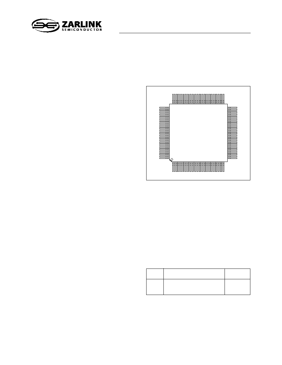
GP
1020
91
120
61
90
1
30
31
60
GP120
Fig 1 Pin connections - top view
ABSOLUTE MAXIMUM RATINGS
These are not the operating conditions, but are the absolute
limits which if exceeded, even momentarily, may cause perma-
nent damage. To ensure sustained correct operation the device
should be used within the limits given under Electrical Character-
istics.
Supply voltage (V
DD
) from ground (V
SS
):
2
0∑3V to16∑0 V
Input voltage (any input pin):
V
SS
2
0∑3V to V
DD
1
0∑3 V
Output voltage (any output pin): V
SS
2
0∑3V to V
DD
1
0∑3 V
Storage temperature:
2
55
∞
C to 1125
∞
C
RELATED PRODUCTS
Description
35∑42MHz SAW Filter
GPS Receiver Front-End
Part
DW9255
GP1010
Datasheet
Reference
DS3861
DS3076
GP1020
SIX-CHANNEL PARALLEL CORRELATOR CIRCUIT
FOR GPS OR GLONASS RECEIVERS
FEBRUARY 1994

2
GP1020
TYPICAL GPS RECEIVER (Fig. 2)
All satellites use the same L1 frequency of 1575∑42MHz, but different Gold codes, so a single front-end may be used. To
achieve better sky coverage it may be desirable to use more than one antenna, in which case separate front-ends will be needed.
TYPICAL GLONASS RECEIVER (Fig. 3)
Each satellite will use a different `L1' carrier frequency, in the range 1602∑5625 to 1615∑500MHz, with 0∑5625MHz spacing,
but all with the same 511-bit spreading code. The normal method for receiving these signals is to use several front-ends, perhaps
with the first LNA and mixer common, but certainly with different final local oscillators and mixers.
Fig. 3 GLONASS receiver simplified block diagram
Fig. 2 GPS receiver simplified block diagram
GP1020
(MASTER)
SIGN 0
MAG 0
SIGN 1
MAG 1
OPTIONAL SECOND
GP1020
(SLAVE)
V
DD
GND
MASTERRESET
SIGN 0
MAG 0
SIGN 1
MAG 1
V
DD
GND
MASTERRESET
DATA BUS (16)
ADDR BUS (8)
MASTER/SLAVE
1
5V
MASTER/SLAVE
V
SS
V
SS
SLAVECLK
TIC OUT
TIC IN
INT OUT
INT IN
1
5V
DECODE
DECODE
MICROPROCESSOR
SYSTEM
MASTER CLK
SAMPLE CLK
SIGN
MAG
GP1010
&
FILTER
OPTIONAL
SECOND
GP1010
&
FILTER
CS
CS
MULTIPLE ANTENNAS TO GIVE
WIDER SKY COVERAGE
CONTROL
3
NAVIGATION
SOLUTION
V
DD
GND
MASTER/SLAVE
V
SS
1
5V
GP1020
MASTERRESET
DATA BUS (16)
ADDR BUS (8)
DECODE
MICROPROCESSOR
SYSTEM
OSCILLATOR
FREQUENCY
SELECTION
INT OUT
SAMPLE CLK
SIGN
MAG
CHANNEL
SELECTION
AND ADC
SIGN
MAG
CHANNEL
SELECTION
AND ADC
CHANNEL
SELECTION
AND ADC
SIGN
MAG
CHANNEL
SELECTION
AND ADC
SIGN
MAG
CHANNEL
SELECTION
AND ADC
SIGN
MAG
CHANNEL
SELECTION
AND ADC
SIGN
MAG
CHANNEL
SELECTION
AND ADC
FREQUENCY
GENERATOR
SAMP CLK
SIGN 0
MAG 0
SIGN 1
MAG 1
SIGN 2
MAG 2
SIGN 3
MAG 3
SIGN 4
MAG 4
SIGN 5
MAG 5
L-BAND
DOWN
CONVERTER
CS
MASTER
CLOCK
GLONASS FRONT-END
FILTERS, AMPLIFIERS
AND MIXERS
CONTROL 3
NAVIGATION
SOLUTION

GP1020
3
PIN DESCRIPTIONS (See Application Notes, p. 41)
All V
SS
and all V
DD
pins must be used in order to ensure
reliable operation. Several pins, such as Satellite Inputs 2 to
9 Sign and Magnitudes are also used for device testing, but
only as a secondary function.
Description
Type
Register Address, bit 7
Register Address, bit 8
Master or slave mode select
Scan Test mode select
Test Clock select
Serial Test Data Input
Master Reset (active low)
Motorola (hi) or Intel (lo) bus select
Chip Select (active low) for bus
Ground
Positive supply
Bus control - see note 1
Bus control - see note 1
Test Mode Select 2
Test Mode Select 1
Test PRN Pattern Magnitude o/p
Test PRN Pattern Sign output
Satellite Input 2, Magnitude
Programmable Interrupt Timer clock
Positive supply
Ground
Interrupt out to microprocessor
Satellite Input 2, Sign
Satellite Input 3, Magnitude
Satellite Input 3, Sign
Satellite Input 4, Magnitude
Satellite Input 4, Sign
Satellite Input 5, Magnitude
Satellite Input 5, Sign
Satellite Input 6, Magnitude
Satellite Input 6, Sign
Satellite Input 7, Magnitude
Satellite Input 7, Sign
Satellite Input 8, Magnitude
Satellite Input 8, Sign
Satellite Input 9, Magnitude
Satellite Input 9, Sign
Satellite Input 1, Magnitude
Satellite Input 1, Sign
Ground
Positive supply
Satellite Input 0, Magnitude
Satellite Input 0, Sign
Sampling clock to down-converter
Positive supply
40MHz Master Clock
Ground
Bias for MASTERCLK in 600mV
AC-coupled mode
Ground
Positive supply
Ground
Sets 100/219kHz to 100or 219kHz
PLL lock status from down-converter
BITE control to down-converter
I/P to monitor GLONASS front-end
20MHz clock from Master to slave
Interrupt to slave to sync to Master
Test Clock 1
Test Clock 2
Test Clock 3
Test Clock 4
Test Clock 5
Test Clock 6
Test Clock 7
Test Clock 8
Pin
No.
1
2
3
4
5
6
7
8
9
10
11
12
13
14
15
16
17
18
19
20
21
22
23
24
25
26
27
28
29
30
31
32
33
34
35
36
37
38
39
40
41
42
43
44
45
46
47
48
49
50
51
52
53
54
55
56
57
58
59
60
61
62
63
64
65
Signal
name
A7
A8
MASTER/
SLAVE
TSCAN
TCKS
TDI1
MASTER
RESET
MOT/INTEL
CS
V
SS
V
DD
WEN
RW
TMS2
TMS1
TMAG
TSIGN
MAG2
100/219kHz
V
DD
V
SS
INTOUT
SIGN2
MAG3
SIGN3
MAG4
SIGN4
MAG5
SIGN5
MAG6
SIGN6
MAG7
SIGN7
MAG8
SIGN8
MAG9
SIGN9
MAG1
SIGN1
V
SS
V
DD
MAG0
SIGN0
SAMPCLK
V
DD
MASTERCLK
V
SS
Bias
V
SS
V
DD
V
SS
CLKSEL
PLLLOCKIN
BITECNTL
GLONASSBIT
SLAVECLK
INTIN
TCK1
TCK2
TCK3
TCK4
TCK5
TCK6
TCK7
TCK8
I
I
I
I
I
I
I
I
I
2
1
I
I
I
I
O
O
I/O
O
1
2
O
I/O
I/O
I/O
I/O
I/O
I/O
I/O
I/O
I/O
I/O
I/O
I/O
I/O
I/O
I/O
I/O
I/O
2
1
I
I
O
1
I
2
O
2
1
2
I
I
O
I
I/O
I
I/O
I/O
I/O
I/O
I/O
I/O
I/O
I
TIC input to slave
TIC output from Master
Data Bus, bit 0
Data Bus, bit 1
Ground
Positive supply
Data Bus, bit 2
Data Bus, bit 3
One pulse per second output
Real time clock interrupt input
Timemark line driver feedback
Timemark line driver feedback
Data Bus, bit 4
Data Bus, bit 5
Positive supply
Ground
Data Bus, bit 6
Data Bus, bit 7
Bus timing mode - see note 2
Test Structure - see note 3
Test Structure - see note 3
Boundary Scan output
Boundary Scan clock
Boundary Scan reset
Test Structure - see note 3
Boundary Scan control
Boundary Scan input
Timemark line driver feedback
Serial Test Data Output 7
On/Off control for LNA by GP1010
Serial Test Data Output 6
Serial Test Data Output 5
Data Bus, bit 8
Data Bus, bit 9
Ground
Positive supply
Data Bus, bit 10
Data Bus, bit 11
Serial Test Data Output 4
Serial Test Data Output 3
Serial Test Data Output 2
Serial Test Data Output 1
Data Bus, bit 12
Data Bus, bit 13
Positive supply
Ground
Data Bus, bit 14
Data Bus, bit 15
Address Latch Enable,
bus control
Register Address, bit 1 (LSB)
Register Address, bit 2
Register Address, bit 3
Register Address, bit 4
Register Address, bit 5
Register Address, bit 6
Pin
No.
66
67
68
69
70
71
72
73
74
75
76
77
78
79
80
81
82
83
84
85
86
87
88
89
90
91
92
93
94
95
96
97
98
99
100
101
102
103
104
105
106
107
108
109
110
111
112
113
114
115
116
117
118
119
120
Signal
name
TICIN
TICOUT
D0
D1
V
SS
V
DD
D2
D3
TIME MARK
RTCINT
MARKFB1
MARKFB2
D4
D5
V
DD
V
SS
D6
D7
WPROG
NANDA
NANDB
TDO
TCK
TRST
NANDOP
TMS
TDI
MARKFB3
TDO7
DISCOP
TDO6
TDO5
D8
D9
V
SS
V
DD
D10
D11
TDO4
TDO3
TDO2
TDO1
D12
D13
V
DD
V
SS
D14
D15
ALE
A1
A2
A3
A4
A5
A6
Description
Type
I
O
I/O
I/O
2
1
I/O
I/O
O
I
I
I
I/O
I/O
1
2
I/O
I/O
I
I
I
O
I
I
O
I
I
I
O
O
O
O
I/O
I/O
2
1
I/O
I/O
O
O
O
O
I/O
I/O
1
2
I/O
I/O
I
I
I
I
I
I
I
MOT/INTEL
1
1
0
0
WEN
1
1
1
0
RW
0
1
0
1
Mode
Motorola
Motorola
Intel
Intel
Function
Write
Read
Read
Write
NOTE 1. The functions of RW and WEN pins depend on whether the
GP1020 is in MotorolaTM (MOT/INTEL = `1') or IntelTM mode (MOT/INTEL
= `0'). In Motorola mode, WEN is an enable (active high) and RW is Read/
Write select (`1' = Read). In Intel mode RW is Read, active low, and WEN
is Write, also active low.
NOTE 2. WPROG is used to modify the timing of bus operations; when it
is held HIGH the internal write signal is ORed with ALE to allow time for the
internal address lines to stabilise; when it is held LOW there is no delay
added to write. NOTE 3. NANDOP (pin 90) is the output of a spare gate with
inputs on NANDA (pin 85) and NANDB (pin 86).

4
GP1020
mA
V
V
k
V
V
k
V
V
µ
A
V
V
k
V
V
k
mV
V
V
V
V
V
V
µ
A
V
V
µ
A
V
V
µ
A
75
75
1
75
75
V
DD
2
0∑5
0∑2
V
DD
2
0∑5
0∑2
V
DD
2
0∑5
0∑2
V
DD
2
0∑5
0∑2
V
DD
2
0∑5
0∑2
ELECTRICAL CHARACTERISTICS
These characteristics are guaranteed over the following conditions (unless otherwise stated):
Supply voltage, V
DD
= 5V
±
10%; Ambient Temperature, T
AMB
= 0
∞
C to 170
∞
C (CG grade),240
∞
C to 185
∞
C (IG grade).
DC CHARACTERISTICS
Supply current, I
DD
, chip fully active
CMOS inputs with pullup resistors to V
DD
: RTCINT,
MASTER/SLAVE, MARKFB (3:1), NANDA, NANDB,
WPROG, ALE
Input voltage high
Input voltage low
Pullup resistor
CMOS inputs with pulldown resistors to V
SS
: MOT/INTEL,
CLKSEL, INT IN, TIC IN
Input voltage high
Input voltage low
Pulldown resistor
CMOS inputs without either pullup or pulldown resistors:
MASTERRESET, CS, WEN, RW, MASTERCLK (note 1),
SLAVECLK, A (8:1), D (15:0), TCK, TDI, TMS, TRST
Input voltage high
Input voltage low
Input leakage current
TTL inputs with pullup resistors to V
DD
: SIGN (9:0),
MAG (9:0), PLLLOCKIN, GLONASSBIT
Input voltage high
Input voltage low
Pullup resistor
TTL inputs with pulldown resistors to V
SS
: TSCAN, TCKS,
TDI1, TMS1, TMS2
Input voltage high
Input voltage low
Pulldown resistor
Input for low level clocks: MASTERCLK (note 1)
Peak to peak sinewave
Power level 1 outputs: TMAG, TSIGN, TDO, TDO (7:1),
NANDOP
Output voltage high
Output voltage low
Power level 3 outputs: 100/219kHz, INT OUT, SAMPCLK,
TIC OUT, BITE CNTL, DISCOP, TIMEMARK
Output voltage high
Output voltage low
Power level 1 outputs with tri-state: MAG (9:2), SIGN (8:2),
TCK (7:1)
Output voltage high
Output voltage low
Output leakage current
Power level 3 output with tri-state: SLAVECLK
Output voltage high
Output voltage low
Output leakage current
Power level 6 output with tri-state: D (15:0)
Output voltage high
Output voltage low
Output leakage current
Bias output: BIAS
Units
Conditions
Max.
Typ.
0∑8V
DD
20
0∑8V
DD
20
0∑8V
DD
2∑0
20
2∑0
20
600
V
DD
2
1
V
DD
2
1
V
DD
2
1
V
DD
2
1
V
DD
2
1
Min.
Value
Characteristic
100
0∑2V
DD
250
0∑2V
DD
250
0∑2V
DD
10
0∑8
250
0∑8
250
0∑4
0∑4
0∑4
10
0∑4
10
0∑4
10
V
SS
<V
PIN
<V
DD
AC coupled
I
OH
= 21∑5mA
I
OL
= 1∑5mA
I
OH
= 24∑5mA
I
OL
= 4∑5mA
I
OH
= 21∑5mA
I
OL
= 1∑5mA
V
SS
<V
PIN
<V
DD
I
OH
= 24∑5mA
I
OL
= 4∑5mA
V
SS
<V
PIN
<V
DD
I
OH
= 29∑0mA
I
OL
= 9∑0mA
V
SS
<V
PIN
<V
DD
Special output to be used only as shown in Fig. 12 (page 8)
NOTE 1.
The input MASTERCLK may be driven by either CMOS logic levels or by a low amplitude sinewave if the BIAS pin is connected as shown
in Fig. 12.
GP1020
5
Address hold time
ALE pulse width
ALE valid to WEN or RW valid (WPROG = 1)
ALE valid to WEN or RW valid (WPROG = 0)
Address valid to ALE low
Address valid to WEN or RW valid
CS high to ALE valid
CS low to WEN or RW valid
Data hold time
Data setup time
RW high to data at high impedance
RW valid to data valid
RW valid to WEN high
WEN low to RW not valid
Write pulse width
CS hold time after RW or WEN not valid
25
50
ns
ns
ns
ns
ns
ns
ns
ns
ns
ns
ns
ns
ns
ns
ns
ns
Max.
TIMING CHARACTERISTICS (See Figs. 4 to 9)
Conditions
Units
Characteristic
Value
10
20
5
20
20
20
10
0
10
30
10
10
15
15
30
0
Min.
Symbol
t
AHOLD
t
ALEPW
t
ALESETUP
t
ALVWRV
t
ASETUP
t
AVWRV
t
CHALV
t
CVWRV
t
DHOLD
t
DSETUP
t
RHDZ
t
RVDV
t
RWVWENH
t
WENLRWNV
t
WLWH
t
WRCH
NOTE. This timing information is based on simulations and is not verified by measurement on each device.
GP1020 BUS TIMING DIAGRAMS
WEN
CS
ALE
A (8:1)
D (15:0)
RW (HIGH)
t
ALESETUP
t
ASETUP
t
AHOLD
ADDRESS VALID
t
ALEPW
t
CVWRV
DATA VALID
t
DSETUP
t
DHOLD
NEXT
R/W
t
WRHCH
t
CHALV
t
WLWH
Fig. 4 Intel 486 mode WRITE. MOT/INTEL = 0, WPROG = 1
(Write inhibited until ALE falling edge)
Fig. 5 Intel 486 mode READ. MOT/INTEL = 0, WPROG = 1
Fig. 6 Intel 186 mode WRITE. MOT/INTEL = 0, WPROG = 0
WEN
CS
ALE
A (8:1)
D (15:0)
RW (HIGH)
t
ALVWRV
t
AHOLD
ADDRESS VALID
t
AVWRV
t
CVWRV
DATA VALID
t
DSETUP
t
DHOLD
NEXT
R/W
t
WRHCH
t
CHALV
t
WLWH
Fig. 7 Intel 186 mode READ. MOT/INTEL = 0, WPROG = 0
RW
CS
ALE
A (8:1)
D (15:0)
WEN (HIGH)
t
ALESETUP
t
ASETUP
t
AHOLD
ADDRESS VALID
t
ALEPW
t
CVWRV
DATA VALID
t
RVDV
t
RHDZ
NEXT
R/W
t
WRHCH
t
CHALV
RW
CS
ALE
A (8:1)
D (15:0)
WEN (HIGH)
t
ALVWRV
t
AVWRV
t
AHOLD
ADDRESS VALID
t
CVWRV
DATA VALID
t
RVDV
t
RHDZ
NEXT
R/W
t
WRHCH
t
CHALV

6
GP1020
GP1020 BUS TIMING DIAGRAMS (continued)
Fig. 8 Motorola 68xxx mode WRITE. MOT/INTEL = 1,
WPROG = 0
Fig. 9 Motorola 68xxx mode READ. MOT/INTEL = 1,
WPROG = 0
t
ALVWRV
t
AVWRV
t
AHOLD
ADDRESS VALID
t
CVWRV
DATA VALID
t
RVDV
t
RHDZ
NEXT
R/W
t
WRHCH
t
CHALV
t
RWVWENH
WEN
CS
ALE
A (8:1)
D (15:0)
RW
t
WENLRWNV
SIGNAL PROCESSING OVERVIEW
Each channel of the GP1020 is fed with a 2-bit (or optionally
with a 1-bit) GPS digital IF at around 1∑4MHz, from the input
multiplexer that connects one of ten signal sources to the
channel input. This signal is first brought to baseband using an
on-chip digital mixer driven by a programmable digital local
oscillator. It is then correlated with a C/A code internally gener-
ated by a programmable Gold code generator; the correlation
result is the sum of the comparisons of individual code chips over
a complete code period (an `epoch' in GPS terminology). A large
positive or a large negative sum indicate good correlation but
with opposite modulation, where the size of `large' will depend on
the current signal to noise ratio, while a small sum indicates poor
correlation and the need to adjust the loops or choose another
satellite.
These results form the `Accumulated Data' and are made
available to the microprocessor to both control the tracking loops
and to give the broadcast satellite data, the `Navigation Mes-
sage' when demodulated. Periodically, the code epoch count,
the code phase, and the carrier phase of all channels, are
sampled at the same instant to form the `Measurement Data' and
are also made available to the processor.
DESCRIPTION OF BLOCKS (see Fig. 10)
CLOCK GENERATOR
The Clock Generator block generates the various clocks
required in the GP1020, which can be operated either as a
master or as a slave device. When it is operated as a master, the
Clock Generator block is driven by a 40MHz clock provided by
the accompanying front-end chip, the GP1010, and to drive the
slaves a 20MHz output SLAVE CLK is provided. When the
GP1020 is operated as a slave, it is driven only by this 20MHz
SLAVE CLK from the master device. In the master the
40MHz is divided in a counter to form seven clock phases to
control the data flow, but to get the same timing in the slaves twin
20MHz dividers use both high and low phases separately to give
the effect of 40MHz clocking.
When in master mode these seven phases are also used to
generate a sampling clock (SAMP CLK) output at 40MHz47 =
5∑71MHz, which drives the data sampling clock input of the
GP1010. A 100/219kHz output is provided for use as a micro-
processor Programmable Interrupt Clock.
TIMEBASE GENERATOR
The Time Base Generator produces, among other signals: a
505∑05
µ
s free-running interrupt timebase INT OUT, a free-
running TIC OUT signal with a period which may be selected to
be either 100ms or 9∑09ms (approximately), and a TIME MARK
signal with a 1 second period as an output which may be locked
to GPS time, UTC, or the receiver timebase by programming its
delay relative to the TIC, based on recent navigation solutions.
The TIC is mainly used to latch measurement data (epoch count,
code phase, code DCO phase and integrated carrier phase
( = DCO phase and cycle count)) of all six channels at the same
instant.
BITE INTERFACE
The Bite Interface block contains a register which allows
control over the built-in-test functions of the chip. In addition, this
register allows the processor to read the state of discrete input
pins, such as PLLLOCKIN connected to the status output of the
GP1010, and also to set the state of the BITE CNTL and the
DISCOP output pins. These can in turn, for example, be used to
drive the GP1010 BITE input pin and the LNA power on/off
select, respectively.
STATUS REGISTERS
The Status Registers block contains registers describing the
status of accumulated and measurement data provided by each
channel.
SIGNAL SELECTION BLOCK
The Signal Selection block contains a multiplexer which can
be programmed to direct any of the ten input sources to any of
the six tracking channels. This is needed in GLONASS where
frequency division multiplexing is used and separate local oscil-
lators are needed to receive each satellite, leading to separate
IF filter channels. An input selector may be desirable in GPS,
which uses code division multiplexing, to allow the use of multiple
antennae to overcome problems of incomplete sky visibility.
For SIGN inputs, LOW = 2, HIGH = 1; for MAG inputs,
LOW = 1, HIGH = 3.
TRACKING MODULE BLOCKS
The six Tracking Module blocks are all identical so that the
term CHx is used in the description to mean any of CH1, CH2,
WEN
CS
ALE
A (8:1)
D (15:0)
RW
t
ALVWRV
t
AHOLD
ADDRESS VALID
t
AVWRV
t
CVWRV
DATA VALID
t
DSETUP
t
DHOLD
NEXT
R/W
t
WRHCH
t
CHALV
t
WLWH
t
RWVWENH
t
WENLRWNV

GP1020
7
MASTER CLK
SLAVE CLK
SAMP CLK
MASTER/SLAVE
SIGN &
MAG
TRACKING
MODULE
CHANNEL 1
TRACKING
MODULE
CHANNEL 2
TRACKING
MODULE
CHANNEL 3
TRACKING
MODULE
CHANNEL 4
TRACKING
MODULE
CHANNEL 5
TRACKING
MODULE
CHANNEL 6
2
TIC
INPUT
SELECTOR
(DUAL
11 TO 7
MUX)
TIMEBASE
GENERATOR
2
10 SETS OF
SIGN & MAG
INPUT
SIGNALS
CLOCKS
CLOCK
GENERATOR
TIC IN
INT IN
INT OUT
TIC OUT
TIMEMARK
STATUS
REGISTER
SELF TEST
GENERATOR
8
7
8
7
7
7
7
7
BITE
INTERFACE
SELF TEST
GENERATOR
STATISTICS
CHECK
MICROPROCESSOR
BUS
TEST
SIGN &
MAG
Fig. 10 Simplified overall block diagram
CH3, CH4, CH5 or CH6 inputs or registers. They have the
architecture shown in Fig. 11. The individual sub-blocks are as
follows:
CARRIER DCO
The Carrier DCO is an accumulator performing additions at a
constant rate and with a programmable increment value. It is
used to synthesise the digital local oscillator signal required to
bring the input signal to baseband in the mixer block, and must
be adjusted away from nominal to allow for Doppler shift and
crystal frequency error. The nominal frequency of the output is
1∑405396825 MHz, set by loading the 26 bit CHx_CARR_INCR
register to 01F7B1B9
H
and is programmed with a resolution of
42∑57475 milliHertz. The very fine resolution is needed to keep
the DCO in phase with the satellite signal.
CODE DCO
This block
is a similar structure to the Carrier DCO block and
is used to synthesise the oscillator signal required to drive the
code generator at the proper chipping rate and phase. The
nominal frequency of the output is 2∑046MHz, to give a chip rate
of 1∑023MHz, and is set by loading the 25 bit CHx_CODE_INCR
register to 016EA4A8
H
and is programmed with a resolution of
85∑14949 milliHertz. Again,the very fine resolution is needed to
keep the DCO in phase with the satellite signal.
CODE GENERATOR
This generates the processor-selected GPS Gold code (one
of PRN code numbers 1 to 32 for normal satellites or 33 to 37 for
ground based use) or the GLONASS code (fixed for all satellites)
or one of eight INMARSAT codes. Twin generators are used to
produce both a prompt (on-time) pattern and an early, late, or
early-minus-late version for tracking use. At the end of each code
sequence a signal DUMP is generated to latch the Accumulated
Data, separately for each channel.
MIXER AND CORRELATOR
The Mixer and Correlator first mixes the digitised input signal
with the Carrier DCO digital local oscillator to generate a signal
at baseband, and then uses the Code Generator outputs to
correlate the data stream. The block includes in-phase and
phase-quadrature channels, as well as prompt and dithered (or
early/late) correlator arms.
The term dither is used in the GP1020 to mean a code channel
in which the timing alternates one half-chip either before or after
the prompt channel, and not the now obsolete technique of Tau-
dither, in which the prompt arm timing is oscillated a little each
side of nominal to give tracking with only one arm.
QUADRUPLE INTEGRATE AND DUMP
The bit-by-bit results from the correlator are passed to the
Quadruple Integrate And Dump block, which integrates the
correlation result of individual code chips from all four correlators
(in-phase and phase-quadrature, prompt and dithered arms)
over a complete code period. Through the Accumulated Data
registers, the processor has access to each integration result.
NAVIGATION OR TIME REFERENCE RECEIVER
HARDWARE SYSTEM DESIGN
A receiver system can use one or more GP1020s. When only
one is used, that IC is operated in master mode, and when more
than one are used, one of them is designated as being the
master
and all of the others are operated as
slaves. In all cases, the
master chip is the one which will receive the 40MHz MASTER
CLK from the GP1010 and generate, upon release of the
MASTERRESET signal, a gated 20MHz clock which drives all
slaves (if any) and allows a synchronised start-up. The master
device also generates the SAMP CLK signal which drives all of
the GP1010 front-ends.
The operating mode is programmed by tying the MASTER/
SLAVE pin to V
DD
for master or to V
SS
for slave operation. The
operating mode sets the functions of MASTER CLK, SLAVE
CLK and SAMP CLK pins.
The TIME MARK signal is generated by the master GP1020;
the slave TIME MARK generator, although not disabled, is not
synchronised with the master. The TIC signal is generated by the
master and routed to the slaves to ensure a common measure-
ment data sampling instant for all the tracking channels. The
slave TIC OUT signal is not disabled but is not used.
The master INT OUT drives the slaves' INT IN pins to provide
latching of status bits at a common instant. Optionally, the slave
TIC OUT and INT OUT pins could be connected to the master
TIC IN and INT IN pins, respectively, for testing purposes.
When more than one GP1020 is used in the same system, the
devices must share a common TIC for sampling of measure-
ment data to enable the software to calculate clock bias in the
pseudoranges, and so find the correct ranges. Each GP1020
contains a state machine driven by 7 different clock phases,
so for two GP1020s to share a common TIC, the devices must
be synchronised. This is achieved by configuring the hard-
ware as follows:
∑
All GP1020s share the same MASTERRESET signal.
∑
One GP1020 is designated the master chip. It is

8
GP1020
1k
BIAS
5k
10n
1-10n
600mV
FROM
GP1010
MASTER CLK
GP1020
INTERNAL CIRCUIT
Fig. 12 Biasing circuit for master clock
INPUT
SIGN & MAG
4∑3MHz IF
SAMPLED
AT5∑7MHz
TO GIVE
1∑4MHz
INTO
GP1020
(VIA INPUT
SELECTOR)
MICROPROCESSOR BUS
14-BIT ACCUMULATE
AND DUMP
CLOCK TIC
CODE
GENERATOR
CODE
DCO
EPOCH
COUNTERS
CLOCK TIC
Q_EOL
14-BIT ACCUMULATE
AND DUMP
Q_PROMPT
EOL C/A
PROMPT C/A
14-BIT ACCUMULATE
AND DUMP
I_EOL
14-BIT ACCUMULATE
AND DUMP
I_PROMPT
4
4
4
1
4
CARRIER CYCLE
COUNTER
CLOCK TIC
CARRIER
DCO
CLOCK TIC
4
4
3
3
IN-PHASE BASEBAND
QUADRATURE BASEBAND
Cos (vt)
1∑4MHz
Sin (vt)
1∑4MHz
2
Fig. 11 Tracking module simplified block diagram
SAMP CLK
40MHz47 = 5∑7142857MHz output when the chip is in
master mode; nominal mark:space ratio is 1:1. This signal is held
low during an active MASTERRESET and when in slave mode.
TICOUT
Output signal from TIC generator, used to sample measure-
ment data and so initiate a navigation solution. TIC does not
drive the microprocessor directly but sets a flag in
MEAS_STATUS_A , which should be be examined by reading
the register periodically, such as at every INT OUT.
TIC OUT is active high; active time duration is either 4∑54545ms
for a short TIC or 9∑0909ms for a long TIC. The rising edge of TIC
OUT is in advance of the effective sampling instant inside the
device by 125ns. The TIC period is selectable via the TIC_PERIOD
bit of TIMER_CNTL register to either 100ms minus 100ns (=
99∑9999ms) or to 9.0909 ms.
TIC IN
The TIC IN input of a GP1020 is normally provided by a
companion GP1020. Its use is controlled by the TIC_SOURCE
bit of the TIMER_CNTL register and is configured in most
applications so the master TIC OUT drives the slave TIC IN.
programmed into this mode by tying the MASTER/SLAVE
pin to V
DD
(or by leaving it unconnected and relying on an
internal pull-up resistor.)
∑
All other GP1020s are designated slaves and are
programmed into this mode by tying their MASTER/
SLAVE pin to V
SS
.
∑
The master GP1020's SAMP CLK output drives all
of the GP1010 front-ends. This ensures that in a multiple
GP1010 application, all of the signals are being sampled
at the same instant in all GP1010s. The slave GP1020s
have their SAMPLING CLK output left unconnected.
∑
The SLAVE CLK output from the master drives the
SLAVE CLK inputs on all slaves.
When the MASTERRESET is released, the clock generators
of all devices ≠ master and slaves ≠ are enabled. The SLAVE
CLK output of the master device will start to toggle only after the
master's clock generator has reached a certain phase (200ns
after the MASTERRESET release). The clock generator of the
slave device gets reset into a state which corresponds to the next
phase and starts counting as soon as the SLAVE CLK signal
from the master reaches its SLAVE CLK input pin.
IMPORTANT TIMING SIGNALS IN A TYPICAL
HARDWARE DESIGN
MASTER CLK
The MASTER CLK is a 40MHz clock which sets the timing of
all functions in a GPS receiver using the GP1020. In a multiple
GP1020 system only the master is given this clock and this may
be connected in either of two ways, depending on the signal
level. If the clock is a TTL signal it is directly connected to the
MASTER CLK input and the BIAS output pin is left unconnected.
The other option is an AC-coupled 600 mV peak-to-peak signal,
when the BIAS output is used to set the DC voltage of the
MASTER CLK pin as shown in Fig. 12. The MASTER CLK pin on
each slave GP1020 is not used and should be tied to V
DD
or V
SS
.
SLAVE CLK
20MHz with 1:1 nominal mark:space ratio. Output from
master GP1020, input to slave, using a bidirectional buffer
controlled by MASTER/SLAVE. This signal is held low when the
master chip is reset and starts to toggle within 200ns after
MASTERRESET is released.

GP1020
9
(e.g. ARINC 743 may be wanted) or a simple reference time
clock may be built.
To synchronise TIME MARK to GPS time the first stage is to
acquire the measurement data at any arbitrary TIC and then
calculate the full navigation solution to give the time at that TIC.
From this determine a later TIC at which to acquire data again
such that after the navigation solution computation delay (typi-
cally a few TIC periods long) a further delay may be programmed
into DOWN_COUNT_HI and _LO registers to start on the next
TIC, to give TIME MARK at the required GPS whole second. This
is rather a long process to get started, but once the first correct
TIC choice and down counter delay are known the process can
roll on with each TIC and delay calculation coming from the
previous navigation solution.
To get UTC instead of GPS time it is only neccessary to read
the navigation message to get the number of whole seconds
difference and add this to the calculated GPS time. A possible
refinement is to calculate the oscillator drift over several meas-
urements and use this to extrapolate a better value for the delay
counter. The ultimate accuracy that can be achieved is very
good, but to get this the crystal must both have high stability and
be drift compensated in the software; in addition, the receiver
front-end delay must be known and allowed for, and the delay
through the output drivers and cables must be allowed for by
using the MARKFBx pins.
If, as is likely, Selective Availability is on it will be the main
source of error in a well designed TIME MARK system, but better
than one microsecond absolute accuracy is still possible. To
reduce the effects of SA it is possible to use a stable rubidium
reference oscillator and average the induced offsets over a long
time to give very good peak errors of a few tens of nanoseconds.
As the main purpose of the TIME MARK output is a timing
reference signal at one pulse per second for the electronic
systems in an airliner, it must be both accurate and known to be
accurate.
The accuracy is achieved by loading DOWN_COUNT_HI
and _LO with the correct offset in 50ns units from the GPS
measuring TIC. As the TIC rate is nominally 1ppm less than
10Hz, the DOWN_COUNT value should be expected to in-
crease at around 1
µ
s per one second TIME MARK, a number
change of 120 each pulse. This value will need continuous fine
tuning to allow for the stable and variable crystal errors.
Integrity is ensured in two ways; first, by using PROP_DELAY
to check the delay through line drivers and to verify that a TIME
MARK really did occur and, secondly, by having a complex
handshake sequence so that any failure in the hardware will be
detected by the microprocessor. The handshake sequence is:
1. Write to DOWN_COUNT_LO to arm the TIME MARK gen-
erator (this requires that DOWN_COUNT_HI is already
written; as it rarely changes,this is often automatically true).
2. At next TIC the GP1020 will start DOWN_COUNT.
3. The GP1020 will give a TIME MARK pulse output and start
the PROP_DELAY counter.
4. Feed TIME MARK back through MARK_FBx input to stop
PROP_DELAY and to set MARK_FB_ACK in
MEAS_STATUS_A
5. Read MEAS_STATUS_A, normally as part of the Measure-
ment Data transfer protocol but, on this occasion, to also
clear the overwrite protection on PROP_DELAY and to clear
the MARK_FB_ACK bit.
6. Read PROP_DELAY, once MARK_FB_ACK has been set
(and cleared) to give a stable value for the last delay. This
also re-enables the TIME MARK generator ready for a repeat
of step (1) to take effect.
This may seem rather complicated, but is only needed once
per second and so is little overhead if a simple system is all
that is required. For a full accuracy system, the various
register operations fit in with the computations needed to
achieve full ARINC 743 specification.
INT OUT
This output signal is a free running interrupt timebase which
may be used to interrupt the microprocessor to initiate data
transfer sufficiently often that no correlation results will be
missed. The tracking loops rely on the microprocessor to adjust
the DCO registers in response to signal changes so the rate of
interaction must be sufficiently high. If the frequency of INT
OUTis too high for the software to process then a polling scheme
may be used, by inhibiting the interrupts (INT_MASK bit in
TIMER_CNTL set low) and then periodically writing to
STATUS_LATCH and reading the status registers to check if
new data is available.
The period of INT OUT is programmable; a typical value is
505∑05
µ
s. During MASTERRESET the interrupt output is stopped
and the pin is held LOW if in Intel mode, or HIGH if in Motorola
mode. The active duration of INT OUT (HIGH for Intel, LOW for
Motorola) is 252∑525
µ
s, which should be more than adequate to
ensure that the interrupt controller in the processor will have time
to respond.
INT IN
This input signal is normally provided by the INT OUT output
of a companion GP1020; in general the master drives the slave.
It is used, when selected via the INT_SOURCE bit of the
TIMER_CNTL register, to latch the state of the status bits.
100kHz/219kHz
A clock output at either 100kHz or 219kHz which may be used
to drive the microprocessor interrupt timer. The frequency is set
by the level on CLKSEL (HIGH for 100kHz and LOW for 219kHz).
MASTERRESET
When MASTERRESET is set LOW , all the registers, accu-
mulators and counters are cleared, except CHX_CNTL, which IS
initialised to specific values (refer to detailed description of the
registers for these values). When the device is held reset, by
MASTERRESET set low, the following pins are driven as listed:
MASTER CLK: This input may or may not be being exter-
nally driven during the reset.
MASTERRESET internally gates MASTER
CLK to ensure a well defined level on all
clock lines until the release of
MASTERRESET; the release of
MASTERRESET must occur only when the
input buffer is properly biased and the input
signal is stable.
SLAVE CLK:
Configured as an input on slave devices and
held LOW on master device.
SAMP CLK:
Held LOW.
100/219kHz:
This output is held LOW when MASTER
RESET is active (also LOW) and toggles to
HIGH shortly after MASTERRESET is
released, and then runs normally.
D0-D15:
High impedance.
BITE CNTL:
LOW.
DISC OP:
LOW.
TIC OUT:
LOW.
INT OUT:
This output is held LOW until interrupt inhibit
is removed, when in Intel bus type mode, or
is held HIGH until the inhibit is re-
moved, when in Motorola bus type mode.
TIME MARK
The primary purpose of the TIME MARK output is to give a
one pulse per second signal locked to UTC or GPS time. This
may be followed by the correct time from the microprocessor and
could be used as a reference by other navigation instruments

10
GP1020
Bit setting
7654 3210
0001 0101
0010 0110
0011 0111
0100 1xx0
0000 1xx0
0001 1xx1
0000 0111
0001 1xx0
0010 1xx1
0001 0010
0010 0011
0100 0101
0101 0110
0110 0111
0111 1xx0
1xx0 1xx1
0000 0011
0001 0100
0010 0101
0011 0110
0100 0111
0101 1xx0
0000 0010
0011 0101
0100 0110
0101 0111
0110 1xx0
0111 1xx1
0000 0101
0001 0110
0010 0111
0011 1xx0
0100 1xx1
0011 1xx1
0000 0110
0001 0111
0011 1xx1
GPS PRN
reference
number
1
2
3
4
5
6
7
8
9
10
11
12
13
14
15
16
17
18
19
20
21
22
23
24
25
26
27
28
29
30
31
32
33*
34* = 37
35*
36*
37* = 34
Selected taps
to be EXORed
together
2
3
4
5
1
2
1
2
3
2
3
5
6
7
8
9
1
2
3
4
5
6
1
4
5
6
7
8
1
2
3
4
5
4
1
2
4
6
7
8
9
9
10
8
9
10
3
4
6
7
8
9
10
4
5
6
7
8
9
3
6
7
8
9
10
6
7
8
9
10
10
7
8
10
SATELLITE CODE SELECTION
This section describes the code selection for normal GPS and
GLONASS operation; for INMARSAT codes and unusual tech-
niques see full details in DETAILED DESCRIPTION OF REGIS-
TERS section, under CHx_CNTL. The same section gives
details of the other bits of CHx_CNTL.
The satellite code to be used by each channel is set by the
CHx_CNTL registers, which are addressed individually from the
A8-A1 address bus by:
00
H
: Read/Write to Channel 1
10
H
: Read/Write to Channel 2
20
H
: Read/Write to Channel 3
30
H
: Read/Write to Channel 4
40
H
: Read/Write to Channel 5
50
H
: Read/Write to Channel 6
70
H
: Write only, to all channels simultaneously
The one GLONASS code may be selected by setting bit 10
HIGH, otherwise this bit should be set LOW and bits 7 to 0 used
to select one of the GPS Gold codes (see Table opposite).
SOFTWARE REQUIREMENTS
The very wide variety of types of GPS or GLONASS receiver
need to operate the correlator in different ways so, to accomodate
this and also to allow dynamic adjustment of loop parameters,
the GP1020 has been designed to use software for as many
functions as possible. This flexibility means that the device
cannot be used without a microprocessor closely linked to it, but
as a processor is always needed to convert the output of the
GP1020 into useful information this is not a significant limitation.
The software associated with the GP1020 can be divided into
two separate modules: one to acquire and track satellite signals
to give pseudoranges and another to process these to give the
navigation solution and format it in a form suitable for the user.
For the Navigation Solution to be possible all of the pseudoranges
must have exactly the same clock error, which can then be
removed iteratively to give real ranges if sufficient satellites are
tracked (3 if the height is known, otherwise 4). This need for exact
matching of timing errors explains the need for all of the compli-
cated synchronisation between all channels and between mas-
ter and slaves.
The following relates only to the signal processing aspects of
the software, to acquire and track signals from up to six satellites
per GP1020 and to obtain the pseudoranges and the navigation
message. The operation of the navigation software is not
dependent on the details of the correlator, and so does not need
to be included in this data sheet.
An on-chip interrupt time base INT OUT is provided to help
implement a data transfer protocol between the microprocessor
and the GP1020 at fixed time intervals, otherwise a software
based polling scheme will be needed ≠ the choice is set by the
application. If INT OUT is used, and perhaps also if polling is
used, the data transfer rate is about twice the correlation result
rate for each channel, so many transfers will not give new data.
Bus use can be reduced by examining the status registers before
each transfer to see if new data is available and then only reading
the data if it useful.
It is important to note that the timing of each of the correlator
channels will be locked to its own incoming signal and not to each
other or to the microprocessor interrupts, so new data is gener-
ated asynchronously. The sampling instant of measurement
data of all channels, however, is common to give a consistent
navigation solution.
In order to acquire lock to the satellites as quickly as possible,
the data from the last fix should be stored as a starting point for
the next fix. It is also useful to have a real-time clock built into the
receiver to give a good estimate of GPS time for the next fix; the
navigation solution can be used to measure clock drift and
calculate a correction for the clock to overcome ageing. The
user's location (or a good estimate of it) along with the Almanac
and the correct time will indicate which satellites should be
searched for and may be used to find an estimate of Doppler
effects, while the previous clock error is the best available
estimate of the present clock error. If this information is not
available then the receiver must scan a much wider range of
values, which will greatly increase the time to lock. The satellite
Clock Correction and Ephemeris are needed for the navigation
solution, so if a recent set is held in memory the calculations may
begin as soon as lock is achieved and not need to wait for the re-
transmission (18 to 36 seconds).
This description applies to just one tracking channel but is the
samd this is not necessarily the same as the other channels.
The GP1020 contains four different types of registers:
∑
Control Registers which are used to program functions of
the device.
∑
Status Registers which provide a status indication of the
process taking place in the device.
∑
Accumulated Data Registers which provide the results
of correlation with the C/A code every millisecond. This is the
raw data used to acquire and track satellite signals.
∑
Measurement Data Registers which latch the carrier DCO
phase, carrier cycle count, code DCO phase, 1 millisecond
GPS Gold codes. *Note that these codes, 33 to 37, are
reserved for non-satellite use only.

GP1020
11
epoch, and the 20 millisecond epoch count at every 9.09 or
100 milliseconds interval. This is the raw data used to
compute pseudorange.
SOFTWARE SEQUENCE FOR ACQUISITION
Satellite signals seen by a GPS receiver are so weak that they
are buried in the noise and can only be detected by correlation.
The spectrum of each signal is spread, using 1023 chip Gold
codes for GPS or a 511 chip maximal length code for GLONASS;
to correlate them therefore, a locally generated code must be
chosen to precisely match the spreading code type, rate, and
phase. This pattern is then multiplied bit-by-bit with the incoming
data stream and the results integrated over the code length to
recover the signal.
The process of signal acquisition is simply the matching of
receiver settings to the actual signal values. To make matters
more complicated the satellite carrier frequency is shifted a little
by the Doppler effect due to the motion of the satellite, the user
clock will drift randomly, and (in most situations) the signal to
noise ratio is poor for some satellites. As a result, the software
must be `wide-band' to find the signal and also `narrow-band' to
reduce noise, leading to very different programs in different
applications. For all tracking channels, the signal processing
software needs the following sequence of activities:
1. Program CHx_CNTL register to select the desired GPS
Gold code (PRN number) for the selected satellite and code type
for the mode of the correlator dithering arm ≠ it is often best, when
in acquistion mode, to fix the dithering arm at early or at late and
do a search in two phases at once and then switch to a tracking
mode once a satellite is found.
2. Program CHx_CARR_INCR_LO and CHx_CARR_INCR_HI
The values programmed into these two registers are concatenated
and set the local oscillator frequency for the digital mixing
performed in the GP1020 to bring the incoming 2-bit digitised
signal down to baseband. The value to be programmed is equal
to the nominal local oscillator frequency plus the estimated
Doppler shift compensation plus the estimated user clock
frequency drift compensation.
3. Program CHx_CODE_INCR_LO and CHx_CODE_INCR_HI
The value to be programmed in these registers represents twice
the nominal chipping rate of the C/A code (2.046 MHz) plus, if
desired, a small compensation for the Doppler shift and for the
user clock frequency drift.
4. Release the tracking channel reset by programming the
RESET_CNTL Register with the proper value. This will cause
the correlation process to start.
5. Obtain accumulated data from Accumulated Data Register
readings. Several consecutive readings on the same tracking
channel can be added to increase, at will, the integration period
of the correlation.
6. Decide if the GPS signal has been found by comparing the
correlation result with a threshold. If found then jump to a signal
pull-in algorithm. Note that both in-phase and phase quadrature
accumulated data have to be considered since at this time, the
carrier DCO local oscillator phase is not necessarily in phase with
the incoming GPS signal.
7. If the GPS signal has not been found, a new trial has to be
made with different carrier DCO, code DCO, or Gold code phase
programmings. Typically, both DCOs would be held constant
while the Gold code phase is varied to try all of the 2046 half chip
positions possible, then the carrier DCO would be programmed
with slightly different values and the Gold code phase positions
would again be scanned. The Gold code phase is varied by
programming the CHx_CODE_SLEW Register and can be
varied by increments of half a code chip.
8. Once the GPS signal has been found, the code phase
alignment, the carrier phase alignment and the Doppler and user
clock bias compensations are still coarse. The code phase
alignment is only within a half code chip, the carrier DCO is not
in phase with the incoming signal and its frequency is still in error
by up to the increment used for successive trials.
The signal processing software must next use a pull-in
algorithm to refine these alignments. There are many suitable
types of algorithm to choose from, such as successive small
steps until the error is too small to matter, like an analog PLL, or
by using more complicated signal processing to estimate the
errors and jump to a much better set of values. The signal pull-
in algorithm will then program CHx_CARR_INCR_LO/HI regis-
ters with more accurate values for the Carrier DCO. Corrections
to the Gold code phase smaller than a half chip cannot be done
by programming CHx_CODE_SLEW registers in the Code
Generator, but should set CHx_CODE_INCR_LO/HI registers
to steer the Code DCO and gradually bring the Gold code phase
to the right value.
SIGNAL TRACKING
The incoming GPS signal will exhibit a Doppler shift which
varies with time due to the non-uniform motion of the satellite
relative to the receiver, and the user clock bias is likely to also
vary with time. The net result is that unless dynamic corrections
are applied to the code and carrier DCOs, the GPS signal will be
lost. This leads to two servo loops being required: one to maintain
lock on the Gold code phase and a second to maintain lock on
the carrier. With the GP1020 these servo loops are implemented
in the signal processing software.
The raw data used to steer the two servo loops is the
Accumulated Data, which is output by the tracking channel at the
rate of once per millisecond. The dithering arm Accumulated
Data is used for the Gold code loop; some approaches use an
`early minus late' Gold code to implement a null steering loop,
others use a dithering code which alternates between a code one
half chip late and a code one half chip early. In the GP1020, the
dithering rate is 20 ms (20 code epochs) each way, starting with
Early after a reset, when this type of code is selected through the
CHx_CNTL register. The Gold code loop is closed by regularly
updating the code DCO frequency using the
CHx_CODE_INCR_LO/HI registers.
The prompt arm Accumulated Data is used for the carrier
phase loop (although the dithering arm may also be used). One
approach consists of varying the carrier DCO phase in order to
maintain all the correlation energy in the in-phase correlator arm
and none in the phase quadrature correlator arm. The carrier
phase loop is closed by regularly updating the carrier DCO
frequency using the CHx_CARR_INCR_LO/HI registers.
DATA DEMODULATION
The C/A code is modulated with Space Vehicle (SV) data at
50 Baud to give the navigation message. This modulation is an
exclusive-OR function of the C/A code with the SV data. This
means that every 20 milliseconds (which is every 20 C/A code
epochs), the C/A code phase will be reversed (shifted by 180
degrees) if the new data bit is different from the previous one. On
the prompt arm, once the signal is being correctly tracked, such
a data bit transition will change the sign of the accumulated data.
Data demodulation can then be achieved in two stages:
1. Locate the instants of data bit transitions to identify which
C/A code epoch corresponds to the beginning of a new data bit.
This will allow initialisation of the GP1020 epoch counters by the
signal processing software (through the CHx_1MS_ and 20MS≠
EPOCH registers) to count code epochs from 0 to 19 in phase
with data bits. At each new cycle of the 1 ms epoch counter, the
20 ms epoch counter will increment.

12
GP1020
2. Record the sign of accumulated data on the prompt arm for
each data bit period of 20 ms, with filtering to reduce the effect of
noise on the signal. Note that there is a sign ambiguity in the
demodulation process in that it is not possible to tell which data
bits are `0's and which are `1's from the signal itself. This
ambiguity will be resolved at a later stage when the full Naviga-
tion Message is interpreted.
PSEUDORANGE MEASUREMENT
The measurement data registers provide the raw data neces-
sary to compute the pseudorange. This raw data is a sample, at
a given instant set by the GP1020 TIC, of the 20 ms and 1 ms
epoch counters, the C/A code phase counter and the code DCO
phase. By definition, the pseudorange is expressed in time units
and is equal to the satellite-to-receiver propagation delay plus
the user clock bias. The user clock bias is first estimated (blind
guessed is more likely with a cold start, but iteration then takes longer)
and then obtained as a by-product of the navigation solution. The
pseudorange is equal to the user's apparent local time of reception
of the signal (t
1
) minus the GPS real time of transmission (t
2
).
With the demodulated data, the software has access to the
Space Vehicle Navigation Message, which contains information on
the GPS system time for the transmission of the current subframe;
this is equal to term t
2
.
The time information in the navigation message allows the
receiver time to be initialised with a resolution of 20 milliseconds (one
data bit period) but with knowledge of the precision to much better
than one C/A code chip ≠ a little less than 1 microsecond. As the time-
of-flight from the satellite to the receiver is in the region of 60 to 80
milliseconds an improved first guess for local time could include an
allowance for this delay to reduce the iteration time later.
By using the data to time-tag the TIC, along with the values of the
Epoch counter, the Code generator phase, and the Code clock
phase it is possible to measure the time of the SV signal in local
apparent time. This gives the value of t
1
needed for the pseudorange
measurement. The pseudorange can now be computed as t
1
2
t
2
.
The error present in the time setting is the initial value of the user
clock bias, with an allowance for the various counter phases. Once
a Navigation Solution has been found the clock error is precisely
known and may be used for future pseudorange calculations.
Because the receiver clock drifts with time, the clock bias changes
with time and must be tracked by the Navigation software.

GP1020
13
GP1020 REGISTER ADDRESSES AND CONTENT
Overall Memory Map
The GP1020 internal registers are addressed using 8 address lines, A1 to A8. This section gives an overview of the
register names with their addresses. A detailed memory map is shown in the Table of Registers.
Address range
Register Block accessed
(Hex)
00 to 07
Access to control registers of tracking channel 1
10 to 17
Access to control registers of tracking channel 2
20 to 27
Access to control registers of tracking channel 3
30 to 37
Access to control registers of tracking channel 4
40 to 47
Access to control registers of tracking channel 5
50 to 57
Access to control registers of tracking channel 6
70 to 77
For write operations only. Access to all identical control
registers of all tracking channels with one single operation.
The same data gets written in these registers.
80 to 83
Access to Accumulated Data and Measurement Data Status
84 to 9B
Access to In Phase and Quad Phase accumulated data registers
and SBR (Status Bit Reset) commands of all tracking channels.
9C,9D
Access to all identical SBR (Status Bit Reset) commands of all
tracking channels with a single write operation.
A0 to B7
Access to measurement data registers of all tracking channels.
BC to BF
For write operations only. Access to all identical measurement
data registers of all tracking channels with one single
operation. The same data gets written in these registers.
C0 to C8
Access to BITE interface, TIME_BASE_GEN, RESET_CNTL,
signal selector and test registers.
Other addresses not used. Do not access these addresses.
Note 1: Registers are not all READ/WRITE. To minimise the hardware, some addresses are shared between read-only and write-only
registers having different functions. Refer to TABLE OF REGISTERS for more details.
TABLE OF REGISTERS
Address
Register
(Hex)
Read function
Write function
00
CH1_CNTL
CH1_CNTL
01
CH1_TST_CODE_SLEW
CH1_SIG_SEL
02
CH1_EPOCH_CHK
CH1_CODE_INCR_HI
03
CH1_SHIFT_REG
CH1_CODE_INCR_LO
04
not used
CH1_CARR_INCR_HI
05
not used
CH1_CARR_INCR_LO
06
not used
CH1_TST_CODE_PHASE
07
not used
CH1_TST_CYCLE
08
not used
not used
09
not used
not used
0A
not used
not used
0B
not used
not used
0C
not used
not used
0D
not used
not used
0E
not used
not used
0F
not used
not used
10
CH2_CNTL
CH2_CNTL
11
CH2_TST_CODE_SLEW
CH2_SIG_SEL
Continued...

14
GP1020
TABLE OF REGISTERS (continued)
Address
Register
(Hex)
Read function
Write function
12
CH2_EPOCH_CHK
CH2_CODE_INCR_HI
13
CH2_SHIFT_REG
CH2_CODE_INCR_LO
14
not used
CH2_CARR_INCR_HI
15
not used
CH2_CARR_INCR_LO
16
not used
CH2_TST_CODE_PHASE
17
not used
CH2_TST_CYCLE
18
not used
not used
19
not used
not used
1A
not used
not used
1B
not used
not used
1C
not used
not used
1D
not used
not used
1E
not used
not used
1F
not used
not used
20
CH3_CNTL
CH3_CNTL
21
CH3_TST_CODE_SLEW
CH3_SIG_SEL
22
CH3_EPOCH_CHK
CH3_CODE_INCR_HI
23
CH3_SHIFT_REG
CH3_CODE_INCR_LO
24
not used
CH3_CARR_INCR_HI
25
not used
CH3_CARR_INCR_LO
26
not used
CH3_TST_CODE_PHASE
27
not used
CH3_TST_CYCLE
28
not used
not used
29
not used
not used
2A
not used
not used
2B
not used
not used
2C
not used
not used
2D
not used
not used
2E
not used
not used
2F
not used
not used
30
CH4_CNTL
CH4_CNTL
31
CH4_TST_CODE_SLEW
CH4_SIG_SEL
32
CH4_EPOCH_CHK
CH4_CODE_INCR_HI
33
CH4_SHIFT_REG
CH4_CODE_INCR_LO
34
not used
CH4_CARR_INCR_HI
35
not used
CH4_CARR_INCR_LO
36
not used
CH4_TST_CODE_PHASE
37
not used
CH4_TST_CYCLE
38
not used
not used
39
not used
not used
3A
not used
not used
3B
not used
not used
3C
not used
not used
3D
not used
not used
3E
not used
not used
3F
not used
not used
40
CH5_CNTL
CH5_CNTL
41
CH5_TST_CODE_SLEW
CH5_SIG_SEL
42
CH5_EPOCH_CHK
CH5_CODE_INCR_HI
43
CH5_SHIFT_REG
CH5_CODE_INCR_LO
44
not used
CH5_CARR_INCR_HI
45
not used
CH5_CARR_INCR_LO
46
not used
CH5_TST_CODE_PHASE
47
not used
CH5_TST_CYCLE
48
not used
not used
49
not used
not used
4A
not used
not used
4B
not used
not used
4C
not used
not used
4D
not used
not used
4E
not used
not used
4F
not used
not used
Continued...

GP1020
15
TABLE OF REGISTERS (continued)
Address
Register
(Hex)
Read function
Write function
50
CH6_CNTL
CH6_CNTL
51
CH6_TST_CODE_SLEW
CH6_SIG_SEL
52
CH6_EPOCH_CHK
CH6_CODE_INCR_HI
53
CH6_SHIFT_REG
CH6_CODE_INCR_LO
54
not used
CH6_CARR_INCR_HI
55
not used
CH6_CARR_INCR_LO
and ADD_DAT_TST
56
not used
CH6_TST_CODE_PHASE
57
not used
CH6_TST_CYCLE
58
not used
not used
59
not used
not used
5A
not used
not used
5B
not used
not used
5C
not used
not used
5D
not used
not used
5E
not used
not used
5F
not used
not used
60 to 6F
not used
not used
70
not used
ALL_CNTL
71
not used
ALL_SIG_SEL
72
not used
ALL_CODE_INCR_HI
73
not used
ALL_CODE_INCR_LO
74
not used
ALL_CARR_INCR_HI
75
not used
ALL_CARR_INCR_LO
76
not used
ALL_TST_CODE_PHASE
77
not used
ALL_TST_CYCLE
78
not used
not used
79
not used
not used
7A
not used
not used
7B
not used
not used
7C
not used
not used
7D
not used
not used
7E
not used
not used
7F
not used
not used
80
MEAS_STATUS_A
STATUS LATCH
81
MEAS_STATUS_B
not used
82
ACCUM_STATUS_A
not used
83
ACCUM_STATUS_B
not used
84
CH1_I_DITH
CH1_MEAS_RST
85
CH1_Q_DITH
CH1_ACCUM_RST
86
CH1_I_PROMPT
not used
87
CH1_Q_PROMPT
not used
88
CH2_I_DITH
CH2_MEAS_RST
89
CH2_Q_DITH
CH2_ACCUM_RST
8A
CH2_I_PROMPT
not used
8B
CH2_Q_PROMPT
not used
8C
CH3_I_DITH
CH3_MEAS_RST
8D
CH3_Q_DITH
CH3_ACCUM_RST
8E
CH3_I_PROMPT
not used
8F
CH3_Q_PROMPT
not used
90
CH4_I_DITH
CH4_MEAS_RST
91
CH4_Q_DITH
CH4_ACCUM_RST
92
CH4_I_PROMPT
not used
93
CH4_Q_PROMPT
not used
94
CH5_I_DITH
CH5_MEAS_RST
95
CH5_Q_DITH
CH5_ACCUM_RST
96
CH5_I_PROMPT
not used
97
CH5_Q_PROMPT
not used
98
CH6_I_DITH
CH6_MEAS_RST
99
CH6_Q_DITH
CH6_ACCUM_RST
Continued...

16
GP1020
TABLE OF REGISTERS (continued)
Address
Register
(Hex)
Read function
Write function
9A
CH6_I_PROMPT
not used
9B
CH6_Q_PROMPT
not used
9C
not used
ALL_MEAS_RST
9D
not used
ALL_ACCUM_RST
9E
not used
not used
9F
not used
not used
A0
CH1_EPOCH_A
CH1_1MS_EPOCH
A1
CH1_EPOCH_B
CH1_PRESET_PHASE
A2
CH1_CARR_DCO_PHASE
CH1_CODE_SLEW
A3
CH1_CARR CYCLE
CH1_20MS_EPOCH
A4
CH2_EPOCH_A
CH2_1MS_EPOCH
A5
CH2_EPOCH_B
CH2_PRESET_PHASE
A6
CH2_CARR_DCO_PHASE
CH2_CODE_SLEW
A7
CH2_CARR CYCLE
CH2_20MS_EPOCH
A8
CH3_EPOCH_A
CH3_1MS_EPOCH
A9
CH3_EPOCH_B
CH3_PRESET_PHASE
AA
CH3_CARR_DCO_PHASE
CH3_CODE_SLEW
and ADD_DAT_TST
AB
CH3_CARR CYCLE
CH3_20MS_EPOCH
AC
CH4_EPOCH_A
CH4_1MS_EPOCH
AD
CH4_EPOCH_B
CH4_PRESET_PHASE
AE
CH4_CARR_DCO_PHASE
CH4_CODE_SLEW
AF
CH4_CARR CYCLE
CH4_20MS_EPOCH
B0
CH5_EPOCH_A
CH5_1MS_EPOCH
B1
CH5_EPOCH_B
CH5_PRESET_PHASE
B2
CH5_CARR_DCO_PHASE
CH5_CODE_SLEW
B3
CH5_CARR CYCLE
CH5_20MS_EPOCH
B4
CH6_EPOCH_A
CH6_1MS_EPOCH
B5
CH6_EPOCH_B
CH6_PRESET_PHASE
B6
CH6_CARR_DCO_PHASE
CH6_CODE_SLEW
B7
CH6_CARR CYCLE
CH6_20MS_EPOCH
B8
not used
not used
B9
not used
not used
BA
not used
not used
BB
not used
not used
BC
not used
ALL_1MS_EPOCH
BD
not used
ALL_PRESET_PHASE
BE
not used
ALL_CODE_SLEW
BF
not used
ALL_20MS_EPOCH
C0
RESET_CNTL
RESET_CNTL
C1
BITE
BITE
C2
RTC_DELAY
TIMER_CNTL
C3
PROP_DELAY_LO
DOWN_COUNT_HI
C4
PROP_DELAY_HI
DOWN_COUNT_LO
C5
STAT_CHK_SIGN
STAT_CHK_SEL
C6
STAT_CHK_MAG
not used
C7
ADD_DAT_TST
ADD_DAT_TST
C8
not used
TDATA_DUTY_CYCLE
C9 to FF
not used
not used

GP1020
17
DETAILED DESCRIPTION OF REGISTERS
The registers are listed in alphabetical order and not in
address order to allow easy reference to each section.
ACCUM_STATUS_A Read Address 82
H
Register bit mapping
Bit
Bit name
LSB 0
CH1_NEW_ACCUM_DATA
1
CH2_NEW_ACCUM_DATA
2
CH3_NEW_ACCUM_DATA
3
CH4_NEW_ACCUM_DATA
4
CH5_NEW_ACCUM_DATA
5
CH6_NEW_ACCUM_DATA
6
not used
7
not used
8
CH1_EARLY_LATEB
9
CH2_EARLY_LATEB
10
CH3_EARLY_LATEB
11
CH4_EARLY_LATEB
12
CH5_EARLY_LATEB
13
CH6_EARLY_LATEB
14
not used
MSB 15
NEW STAT_DATA
REGISTER OPERATION
ACCUM_STATUS_A is a latch register containing the state
of status bits prevailing at time of sampling. The status bits are
sampled and latched on the positive edge of every INT OUT or
INT IN signal. They can also be sampled and latched on request
by performing a write operation to STATUS_LATCH (location
80
H
). Latching the status bits ensures glitch-free reading of
ACCUM_STATUS_A.
BIT DESCRIPTION
The following bits are all active HIGH:
CHx_NEW_ACCUM_DATA status bit indicates if there is
new accumulated data available to be read. Each indi-
vidual bit can be cleared with a write operation at
CHx_ACCUM_RESET location or by disabling the propa-
gation of clocks (CHx_RSTB bits of RESET_CNTL). This
also releases the overwrite protection.
Each bit is also cleared on the trailing edge of a read of
the associated Q_PROMPT register. If new accumulated
data becomes available after ACCUM_STATUS_A bits
have been latched, the overwrite protection is not cleared
while reading the Q_PROMPT register and the
CHx_NEW_ACCUM_DATA bit will be set at the next
latching of ACCUM_STATUS_A.
CHx_EARLY_LATEB status bit indicates whether the
accumulated data on the dithering arm of the tracking
channel results from correlation with early or late code. A
HIGH indicates an EARLY code and a LOW indicates a
LATE code. Each individual bit is updated at each DUMP
when the overwrite protection is not active. When the
Early-Minus-Late code is selected for a particular channel,
this status bit has no meaning.
NEW_STAT_DATA status bit when HIGH indicates that
new statistical data is available in the STAT_CHK_SIGN
and STAT_CHK_MAG registers. It is cleared when a
STAT_CHK_MAG read operation is performed if a valid
state had been latched previously or by a write operation
at ALL_ACCUM_RESET location. The first statistical
data after a power up is not representative and should be
cleared. All status bits are reset by a hardware or software
master reset.
ACCUM_STATUS_B Read Address 83
H
Register bit mapping
Bit
Bit name
LSB 0
CH1_MISSED_ACCUM
1
CH2_MISSED_ACCUM
2
CH3_MISSED_ACCUM
3
CH4_MISSED_ACCUM
4
CH5_MISSED_ACCUM
5
CH6_MISSED_ACCUM
6
not used
7
not used
8
CH1_OVFL_ACCUM
9
CH2_OVFL_ACCUM
10
CH3_OVFL_ACCUM
11
CH4_OVFL_ACCUM
12
CH5_OVFL_ACCUM
13
CH6_OVFL_ACCUM
14
not used
MSB 15
not used
REGISTER OPERATION
ACCUM_STATUS_B bits are sampled and latched on the
positive edge of every INT OUT or INT IN signal. They can also
be sampled and latched on request by performing a write
operation to STATUS_LATCH (location 80
H
).
BIT DESCRIPTION
CHx MISSED_ACCUM status bit indicates if there has
been missed accumulated data. When active HIGH, this
status bit is latched until (i) a master reset (hardware or
software) or (ii) a write operation to CHx_ACCUM_RESET
with don't care data or (iii) the propagation of clocks is
disabled (CHx_RSTB bits of RESET_CNTL).
CHx_OVFL_ACCUM status bit indicates if there has
been an overflow in any of the channel accumulated data
registers. This bit is active HIGH and is updated at each
DUMP when the overwrite protection is not active. It gets
reset whenever the associated CHx_ACCUM_RESET is
written into with don't care data or upon a master reset
(hardware or software) or by disabling the propagation of
clocks (CHx_RSTB bits of RESET_CNTL).
ADD_DAT_TST Read/Write Address C7
H
This register is used to test the address bus and data bus
hardware connections to the inputs of the chip. It allows the
system to verify that there is no short between pins or input lines
in the chip or on the board.
Register bit mapping
Bit
Description
15 to 8
Contents of address bus or most
significant bits of data bus.
7 to 0
Contents of least significant bits of
data bus.
REGISTER OPERATION
This register is a read/write register. Upon a master reset
(software or hardware) the register is cleared. When a write is
performed at address AA
H
or 55
H
the most significant bits of the
register will be loaded with the address bus value present on the
bus, AA
H
or 55
H
if the address bus is working properly and the
least significant bits of the register will keep their previous value.

18
GP1020
When a write is performed at address C7
H
the register will be
loaded with the data bus value present on the bus.
When a read operation is performed to C7
H
it reads all the bits
previously loaded.
It is recommended that the test is performed as follows in
order to verify that the address and data bus operate properly.
Address Bus Test:
∑
Write to address 55
H
(the data bits are don't care)
∑
Read the most significant bits at address C7
H
(the 8 least
significant bits are 00
H
if no access had been done to the
address C7
H
). If the value is not 5500
H
a problem is
detected on the address bus.
∑
Write to address AA
H
(the data bits are don't care)
∑
Read the most significant bits at address C7
H
. If the value
is not AA00
H
a problem is detected on the address bus.
NOTE : When writing to addresses 55
H
and AA
H
, the
CH6_CARR_INCR_LO and CH3_CODE_SLEW registers
will also be written into with the values on the data bus.
Data Bus Test:
∑
Write 5555
H
to address C7
H
∑
Read the register at address C7
H
. If the value is not 5555
H
a problem is detected on the data bus.
∑
Write AAAA
H
to address C7
H
∑
Read the register at address C7
H
. If the value is not AAAA
H
a problem is detected on the data bus.
BITE Read/Write Address C1
H
Register bit mapping
Bit
Description
0
BITECNTL
1
DISCOP
2
PLL_LOCKA (state)
3
PLL_LOCKB (negative transition)
4
GLONASS BIT
5
SELF_TEST_EN
6
SELF_TEST_SOURCE
7
MEANDER
8
CARR_MIX_ENB
BIT DESCRIPTION
BITECNTL bit: Drives the BITE input of the GP1010. Set
inactive LOW by a Master Reset. When HIGH, the
GP1010's PLL is unlocked and the 40 MHz signal be-
comes unstable. The GP1020 should be put into hardware
master reset mode for the time needed to allow the
GP1010's 40 MHz output to stabilise.
DISC O/P: Discrete output with no specific function. LOW
at power up and its state will follow the value written in the
BITE register.
PLL_LOCKA: input from GP1010, Read only, to indicate
the state of the PLL LOCK signal; a HIGH indicates a
locked condition. This discrete input can be used for other
purposes.
PLL_LOCKB: input from GP1010, indicates that a nega-
tive transition of the PLL LOCK signal (from locked to
unlocked state) has been detected and latched in the
GP1020. A HIGH indicates a negative transition. This bit
is cleared by the trailing edge of a read to BITE register
operation.
GLONASS BIT: TEST input from GLONASS front end. A
HIGH on this pin sets register bit HIGH. This discrete input
can also be used for other purposes.
SELF_TEST_EN: active HIGH. When inactive (LOW) the
self-test signal generator is disabled and TSIGN and
TMAG output pins are held LOW. When active the self-test
signal generator is enabled and TSIGN and TMAG output
pins are toggling. The injection back into the input of the
tracking channels is controlled by CHx_SIGNAL_SEL.
SELF_TEST_SOURCE: When LOW, the tracking chan-
nel 1 is used as a signal source for the self-test signal
generator. When HIGH, the tracking channel 2 is used as
a signal source for the self-test signal generator.
MEANDER: When HIGH, the self-test generator will
modulate the data bit stream with a meander. This is
required when GLONASS operation has to be tested.
CARR_MIX_ENB: When LOW, all carrier mixers operate
normally. When HIGH, all carrier mixers are disabled and
the incoming sign and magnitude data passes through
without being affected.
CHx_ACCUM_RESET Write Addresses 85, 89, 8D,
91, 95, 99
H
and ALL_ACCUM_RESET Write Address
9D
H
These are write-only locations provided to allow resetting of
all the status bits associated with a given channel in
ACCUM_STATUS_A and ACCUM_STATUS_B.
ALL_ACCUM_RESET access will also clear the
NEW_STAT_DATA flag in ACCUM_STATUS_B register. When
these locations are written into, the data is don't care. But if the
CNTTESTMODE bit (CHx_20MS_EPOCH register) is active,
G1 and G2 registers will be set at the 1023rd chip of the code
sequence. This operation accelerates the test process by gen-
erating accumulated data and status bits when the code steps to
the first chip and so generating a DUMP in the associated
channel.
CHx_CARR_CYCLE Read Addresses A3, A7, AB,
AF, B3, and B7
H
This register contains the 16 more significant bits of a variable
containing the number of CARRIER DCO cycles that occurred
during the last TIC period ending at a TIC. The value is sampled
and latched on the TIC. While reading measurement data
associated with a given channel, CHx_CARR_CYCLE must be
read last because the trailing edge of a read to this register will
release the overwrite protection mechanism of measurement
data for this channel.
CARR_CYCLE: PRINCIPLE OF OPERATION
In the CHx_CARR_CYCLE register and counter a TIC gen-
erates two consecutive actions:
1. It latches the 16 more significant bits of the cycle up counter
into CARR_CYCLE and the 2 less significant bits into
CARR_DCO_PHASE.
2. It resets the cycle up counter.
After each TIC, every time the carrier DCO accummulator
generates an OVERFLOW as a result of a carrier cycle being
completed, the cycle up counter counts up by one. The number
of bits needed for the counter was established as follows:
For GPS, the nominal CARRIER DCO frequency with no
Doppler and no oscillator drift compensation is 1∑405396825
MHz, so in 100 ms, there will be about 140,540 cycles. For
GLONASS signals, the carrier DCO frequency wil vary depend-
ing on the particular satellite being tuned, between 1∑429 - 0∑6
MHz and 1∑429 + 0∑6 MHz, a maximum of 2∑029 MHz, giving
202,900 cycles in 100 ms.
The maximum number of cycles, CARR_COUNT MAX, will
also depend on the maximum Doppler and oscillator drift com-
pensation to be allowed for, hence the counter must be able to
count to a number greater than 140,540 or 202,900.
The highest frequency required is then 2∑029 MHz plus a few

GP1020
19
tens of kilohertz to allow for oscillator drift and Doppler compen-
sation. An 18 bit counter will cover up to 262,143 cycles, which
is more than adequate.
REGISTER CONTENTS RANGE
CHx_CARR_CYCLE is a 16 bit register, unsigned, and the
validity range of the data is 0 to 2
16
2
1.
CHx_CARR_CYCLE content is protected by the overwrite
protection mechanism of measurement data. Thus for an
overwrite to occur, either the associated
CHx_NEW_MEAS_DATA status bit has to be cleared or
CHx_CARR_CYCLE itself has to be read.
CHx_CARR_DCO_PHASE Read Addresses A2, A6,
AA, AE, B2, B6
Register bit mapping
Bit
Description
9 to 0
Most significant bits of CHx_CARR_DCO
phase accumulator. The weight of the
least significant bit is 2p/1024 radian. These
bits form an unsigned integer valid from
0 to 1023.
CHx_CARR_DCO_PHASE provides the
sub-cycle integrated phase measurement
information and therefore complements
the information given by CHx_CARR_CYCLE
11 and 10
Least significant bits of the number
of carrier DCO cycles that occurred during
the last TIC period ending at a TIC. The
value is sampled and latched on the TIC.
15 to 12
Not used.
The register value is latched on a TIC and protected from
overwrite by the overwrite protection mechanism of measure-
ment data.
ACCUMULATOR
OVERFLOW
2
CARRIER
DCO
ACCUMULATOR
CLK
EN
CYCLE UP
COUNTER
RESET
DATA
LOAD
CARR_CYCLE
REGISTER
LATCH
16
ENABLE
DATA
BUS
CARR_DCO_PHASE
REGISTER
LATCH
TIC
Fig. 13 CHx_CARR_CYCLE block diagram
CHx_CARR_INCR_HI & CHx_CARR_INCR_LO and
ALL_CARR_INCR_HI & ALL_CARR_INCR_LO
Write Addresses 04 & 05, 14 & 15, 24 & 25, 34 & 35,
44 & 45, 54 & 55 and 74 & 75
H
Register bit mapping
Bit
Description
CARR_INCR_HI
9 to 0
More significant bits of the Carrier
DCO phase increment.
CARR_INCR_LO
15 to 0
Less significant bits of the Carrier
DCO phase increment.
REGISTER OPERATION
The registers CARR_INCR_LO and CARR_INCR_HI are
combined to form the 26 bits of the CARR_INCR register, the
carrier DCO phase increment. Both registers are write-only
registers and can be written to at any time. The first write must be
performed on CARR_INCR_HI and the second write on
CARR_INCR_LO. The written value is latched in the CARR_INCR
register on the trailing edge of a write to CARR_INCR_LO. It is
possible to perform a write only to CARR_INCR_LO register if
the CARR_INCR_HI value does not need to be updated.
The DCO adder is 27 bits wide and the LSB of the INCR
register represents a step given by:
Min. Step Freq. = (40MHz/7)32
2
27
= 42∑57475 milliHertz
and the output frequency is:
Freq. out = CHx_CARR_INCR reg. value3Min. Step Freq.
The nominal value of the CHx_CARR_INCR register for GPS
is 01F7 B1B9
H
(to get a carrier at 1∑405396825 MHz when the
GP1010 clock signal is at 40 MHz).

20
GP1020
Register bit mapping
Bit
Description
CODE_INCR_HI
8 to 0
More significant bits of the Code DCO
phase increment.
CODE_INCR_LO
15 to 0
Less significant bits of the code DCO
phase increment.
REGISTER OPERATION
The registers CODE_INCR_LO and CODE_INCR_HI are
combined to form the 25 bits of the CODE_INCR register, the
code DCO phase increment. Both registers are write-only
registers and can be written to at any time. The first write must
be performed on CODE_INCR_HI and the second write on
CHx_CODE_INCR_HI & CHx_CODE_INCR_LO and ALL_CODE_INCR_HI & ALL_CODE_INCR_LO
Write Addresses 02 & 03, 12 & 13, 22 & 23, 32 & 33, 42 & 43, 52 & 53 and 72 & 73
H
CHx_CNTL and ALL_CNTL Read/Write Addresses 00, 10, 20, 30, 40, 50, and 70
H
Register bit mapping
Operation mode
Bit
of CHx_CNTL reg.
Description
(Set by bit 15)
7 to 0
MODE1
C/A CODE SELECTION FUNCTION
9 to 0
MODE2
(see details below)
9 and 8
MODE1
CODESEL(0:1):selects the apppropriate code to be shifted out of the
dithering arm output of the code generator as follows:
9 = 0 8 = 0 Early code
9 = 0 8 = 1 Late code
9 = 1 8 = 0 Dithering code
9 = 1 8 = 1 Early minus late code
10
MODE1&2
GLO/GPSB: Selects the code type to be generated. GLONASS C/A
code when HIGH, GPS or INMARSAT C/A code when LOW.
11
MODE1&2
CODE_OFF/ONB: When LOW, the code is output normally, but when
HIGH, the Prompt, Early and Late codes are held HIGH (no effect on the
mixer outputs) and the Early-minus-late code is held LOW to mask
mixer outputs and force I&D input values to 0.
12
MODE1&2
PRESET/UPDB: While HIGH, Programs the channel to Preset mode, or
while LOW, programs the channel to Update mode.
14 and 13
MODE1
not used - don't care
14 and 13
MODE2
CODESEL(0:1) As bits 9 and 8 MODE1.
15
----
MODE: When LOW the CNTL register is in MODE1 (power up condition)
and when HIGH in MODE2. When in MODE1, the selection of a C/A
code is done by selecting two taps of the G2 register, but in MODE2
by presetting the value of the G2 register. The function of bits 8 and 9
will change depending on the MODE.
REGISTER OPERATION
CHx_CNTL can be written into at any time and any modifica-
tion to its content is effective immediately (within 250 ns) while
in UPDATE mode, or for all bits except PRESET/UPDB at the
next TIC while in PRESET mode. Before reading the content of
this register, it is necessary to wait 250 ns after the last write
operation when in UPDATE mode. Only the PRESET bit is
available immediately but it is cleared 150ns after the PRESET
sequence has taken place (at the TIC following the initialisation
of CHx_20MS_EPOCH register). It is important to program this
register first when starting a PRESET initialisation sequence.
CODE_INCR_LO. The written value is latched in the
CODE_INCR register on the trailing edge of a write to
CODE_INCR_LO. It is possible to perform a write only to
CODE_INCR_LO register if the CODE_INCR_HI value does
not need to be updated.
The DCO adder is 26 bits wide and the LSB of the INCR
register represents a step given by:
Min. Step Freq. = (40MHz/7)32
2
26
= 85.14949 milliHertz
and the output Frequency is:
Freq. out = CHx_CODE_INCR reg. value3Min. Step Freq.
NOTE: The CODE DCO drives the CODE GENERATOR to
give half-chip time steps and so must be programmed to twice
the required chip rate. This means that the chip rate resolution
is 42∑57475 milliHertz.
The nominal value of the CHx_CODE_INCR register for
GPS is 016E A4A8
H
(to get a chip rate of 1.023MHz when the
GP1010 clock signal is at 40 MHz).

GP1020
21
C/A CODE SELECTION
The CHx_CNTL register allows two different modes of pro-
gramming the CODE GENERATOR :
MODE 1: select the appropriate taps of G2 to generate
the GPS C/A code.
MODE 2: set the G2 register with the appropriate pat-
tern to generate the GPS or INMARSAT C/A
codes.
NOTE:
When in MODE 2, the G2 register should be
loaded with a value representing its state at the
time of the second chip.
The difference between the two modes of programming the
C/A code is that MODE 2 allows the CODE GENERATOR to
synthesise the 8 INMARSAT C/A codes and MODE 1 does not,
but is more straightforward.
The following table gives the pattern of bits 3 to 0 or 7 to 4
to select a particular tap (used in MODE 1 of the CHx_CNTL
register) :
Bit
Tap
Pattern
0000 1
0001 2
0010 3
0011 4
0100 5
0101 6
0110 7
0111 8
1xx0 9
1xx1 10
The table below shows the bit setting required to select the
appropriate taps which will decode the 37 possible GPS PRN
signal numbers when in MODE 1 and the bit setting required to
set the G2 register in the second chip state for all GPS and
INMARSAT C/A codes when in MODE 2.
Note that the list does not show all the possible tap and
bit setting combinations. Tap combinations which are not listed
can also be used if required.
GPS PRN
MODE 1
Selected
MODE 2
signal no.
bit setting
taps
bit setting
7 to 0
9 to 0
1
0001 0101
2 EXOR 6
3F6
H
2
0010 0110
3 EXOR 7
3EC
H
3
0011 0111
4 EXOR 8
3D8
H
4
0100 1xx0
5 EXOR 9
3B0
H
5
0000 1xx0
1 EXOR 9
04B
H
6
0001 1xx1
2 EXOR 10
096
H
7
0000 0111
1 EXOR 8
2CB
H
8
0001 1xx0
2 EXOR 9
196
H
9
0010 1xx1
3 EXOR 10
32C
H
10
0001 0010
2 EXOR 3
3BA
H
11
0010 0011
3 EXOR 4
374
H
12
0100 0101
5 EXOR 6
1D0
H
13
0101 0110
6 EXOR 7
3A0
H
14
0110 0111
7 EXOR 8
340
H
15
0111 1xx0
8 EXOR 9
280
H
16
1xx0 1xx1
9 EXOR 10
100
H
17
0000 0011
1 EXOR 4
113
H
18
0001 0100
2 EXOR 5
226
H
19
0010 0101
3 EXOR 6
04C
H
20
0011 0110
4 EXOR 7
098
H
21
0100 0111
5 EXOR 8
130
H
22
0101 1xx0
6 EXOR 9
260
H
GPS PRN
MODE 1
Selected
MODE 2
signal no.
bit setting
taps
bit setting
7 to 0
9 to 0
23
0000 0010
1 EXOR 3
267
H
24
0011 0101
4 EXOR 6
120
H
25
0100 0110
5 EXOR 7
270
H
26
0101 0111
6 EXOR 8
0E0
H
27
0110 1xx0
7 EXOR 9
1C0
H
28
0111 1xx1
8 EXOR 10
380
H
29
0000 0101
1 EXOR 6
22B
H
30
0001 0110
2 EXOR 7
056
H
31
0010 0111
3 EXOR 8
0AC
H
32
0011 1xx0
4 EXOR 9
158
H
33
0100 1xx1
5 EXOR 10
2B0
H
34 *
0011 1xx1
4 EXOR 10
058
H
35
0000 0110
1 EXOR 7
18B
H
36
0001 0111
2 EXOR 8
316
H
37 *
0011 1xx1
4 EXOR 10
058
H
201
n/a n/a
n/a
2C4
H
202
n/a n/a
n/a
10A
H
205
n/a n/a
n/a
3E3
H
206
n/a n/a
n/a
0F8
H
207
n/a n/a
n/a
25F
H
208
n/a n/a
n/a
1E7
H
209
n/a n/a
n/a
2B5
H
211
n/a n/a
n/a
10E
H
*C/A Codes 34 and 37 are common
NOTE: PRN sequences 33 to 37 are reserved for other uses (e.g.
ground transmitters).
The table below lists the required setting of the register bit 0
to generate the GLONASS C/A code or the GLONASS-like test
C/A code. Note that bit 10 must be HIGH to select GLONASS
rather than GPS codes.
Bit 0 setting
Code type
Selected G1 taps
MODE 1 & 2
0
GLONASS
5 EXOR 9
1
GLONASS TEST 3 EXOR 5 EXOR 6 EXOR 9
In update mode, the C/A code generated by the CODE
GENERATOR can be changed at any time but the next accumu-
lated data following the command will not be valid. The MODE
bit cannot be modified without disabling the clock phases when
in UPDATE mode otherwise the C/A code generated will not be
valid. This is not the case when starting a PRESET sequence.
To provide a clean switch between GLONASS and GPS
modes of operation for a specific channel, it is necessary to
proceed as follows: Disable propagation of the clock phases to
this tracking channel by selecting the appropriate bit in the
RESET_CNTL register, then select the desired mode of opera-
tion GLONASS or GPS and re-enable the propagation of the
clock phases. If the clock phases propagation are not disabled,
the next accumulated data will not be valid.
When the dithering code has been selected, the dithering arm
will use the EARLY code for a period of 20 C/A codes, the LATE
code for the next 20 C/A codes and this process of dithering
between EARLY and LATE code will be repeated indefinitely.
The dithering arm will use the EARLY code for the first 20 ms
EPOCH following a SLEW or a PRESET operation.
Upon MASTERRESET, CHx_CNTL bits are set to the
states given in the following Table.
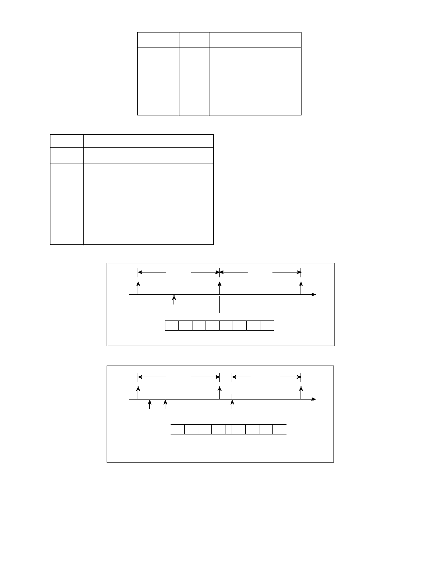
22
GP1020
Bit
State
Description
7 to 0
03
H
GPS PRN No. 17 selected.
9 and 8
00
Early Code on the dithering arm.
10
0
GPS C/A CODE
11
0
CODE ON
12
0
UPDATE MODE
14 and 13
00
N/A (MODE1)
15
0
MODE1
CHx_CODE_SLEW and ALL_CODE_SLEW Write Addresses A2, A6, AA, AE, B2, B6 and BE
H
Register bit mapping
Bit
Description
10 to 0
Unsigned integer ranging from 0 to 2047
representing the number of code half chips to
be slewed after the next DUMP if in
UPDATE MODE or after the next TIC, if in
PRESET MODE. Since there are only 2046
half chips in a GPS C/A code, a
programmed value of 2047 is equivalent to
a programmed value of 1 but the next DUMP
event will take place 1 ms later.
For the GLONASS code a similar wrap-
around will occur at 1023 and 2045.
The CHx_CODE_SLEW register can be written to at any
time. If two accesses have taken place before a DUMP in
UPDATE mode or before a TIC when in PRESET mode, the
latest value will be used at the next slew operation.
When the slew process is being executed, a write access
to the CHx_CODE_SLEW register will cause the transfer of
this new value into the counter and will be used immediately.
The result is not predictable. This situation should be avoided
by synchronising the access with the associated
CHx_NEW_ACCUM_DATA status bit.
Slew timing details are shown in Figs. 14 and 15.
t
1
DUMP:
TIME
Fig. 14 SLEW in UPDATE mode
1021 1022 1023
1
1
1
2
3
1023 CHIPS
1025 CHIPS
C/A CODE CHIP NO. :
t1: Load 4 in the CHx_CODE_SLEW register = 2 chips delay.
DUMP:
TIME
Fig. 15 SLEW in PRESET mode
98
99
100
1
1
1
2
3
1023 CHIPS
1024∑5 CHIPS
C/A CODE CHIP NO. :
t1: Set the PRESET mode (Bit 12 in CHx_CNTL register)
t2: Load 3 in the CHx_CODE_SLEW register (=1∑5 chips delay)
t3: TIC event
t
1
t
2
t
3
4

GP1020
23
CHx_I_DITH, CHx_Q_DITH, CHx_I_PROMPT,
CHx_Q_PROMPT
24 consecutive Read Addresses 84 to 9B
H
Register bit mapping
Bit
Description
15 to 2
Accumulated data registers, which are
loaded on each Dump event with the I&D
accumulator results.
1
Not used, held LOW.
0
Instantaneous value of the over/underflow
flag (for test purposes). Normally LOW,
but HIGH if the data being accumulated in
the I&D accumulator has reached the
over/underflow condition.
REGISTER OPERATION
These registers are read only registers; they can be read at
any time and their content is protected by the overwrite protection
mechanism of accumulated data. The CHx_I_PROMPT and
CHx_Q_PROMPT contain the accumulated data taken on the
Prompt arm. The CHx_I_DITH and CHx_Q_DITH contain the
accumulated data taken on the Dithering arm. The overwrite
protection mechanism is released by reading the
CHx_Q_PROMPT register.
The values contained in the registers are 2's complement
values with the valid range of the data from 2
13
for negative
numbers to (2
13
21) for positive numbers. When an over/
underflow condition is flagged (CHx_OVFL_ACCUM bit in
ACCUM_STATUS_B set HIGH) the contents of the registers for
this arm will be the last I&D accumulator values before the over/
underflow condition happened. If bit 15 is LOW it is an overflow
and if bit 15 is HIGH it is an underflow. Bits 0 of the 24
accumulated data registers have no link with the other data in
these registers. When HIGH, each of these bits indicates that the
data being accumulated in the I&D has reached the maximum
value (positive or negative) of the accumulator and this value will
be available at the next DUMP.
CHx_MEAS_RST and ALL_MEAS_RST
Write Addresses 84, 88, 8C, 90, 94, 98 and 9C
H
A write to this location with don't care data resets all measure-
ment data status bits contained in both MEAS_STATUS_A and
MEAS_STATUS_B registers. It also clears any active overwrite
protection on measurement data. ALL_MEAS_RST access will
also clear the MARK_FB_ACK and the RTC_TIC_ACK flags in
MEAS_STATUS_A register and the associated overwrite pro-
tections.
CHx_PRESET_PHASE and ALL_PRESET_PHASE
Write Addresses A1, A5, A9, AD, B1, B5 and BD
H
Register bit mapping
Bit
Description
7 to 0
Most significant bits of the Code DCO
phase which is to be loaded at next TIC
event if in PRESET mode.
REGISTER OPERATION
In PRESET mode, the 8 bits of the PRESET_PHASE register
are added to the top 7 bits of the CHx_CODE_INCR register
CHx_EPOCH_A
Read Addresses A0, A4, A8, AC, B0, B4
H
This register contains the variables as detailed below.
Register bit mapping
Bit
Description
15 to 11
CHx_1MS_EPOCH: The one millisecond
epoch counter value sampled at TIC
event. Its valid range is 0 to 19.
10 to 0
CHx_CODE_PHASE: Represents the
code phase of the code generator
when sampled and latched on a TIC,
expressed as a number of half code chips.
It ranges from 0 to 2045 when a GPS
C/A code is generated and from 0 to 1021
when a GLONASS C/A code is generated.
CHx_EPOCH_A content is protected from overwrite by the
overwrite protection mechanism of measurement data.
CHx_EPOCH_B
Read Addresses A1, A5, A9, AD, B1, B5
H
The register contains two variables as detailed below:
Register bit mapping
Bit
Description
15 and 14
Not used.
13 to 8
CHx_20MS_EPOCH: Contains the 20
millisecond epoch counter value sampled
at TIC event. Its valid range is from 0 to 49.
7 to 0
CHx_CODE_DCO_PHASE: Contains the
eight most significant bits of the code DCO
phase accumulator sampled at TIC event.
The weight of the least significant bit
is 2p/256 radians, 2p being 1/2 code
chip. The byte is an unsigned integer
valid from 0 to 255.
CHx_EPOCH_B content is protected from overwrite by the
overwrite protection mechanism of measurement data.
CHx_EPOCH_CHK
Read Addresses 02, 12, 22, 32, 42, 52
H
This register contains the instantaneous value of
CHx_1MS_EPOCH and CHx_20MS_EPOCH. It can be used to
verify if the Epoch counters have properly been initialised by the
software since the timing is critical for the initialisation operation.
Its value is not latched and is updated on the occurence of a
DUMP. This register should be read only when there is no
possibility of getting a DUMP during the read cycle.
Register bit mapping
Bit
Description
15 to 13
Not used.
12 to 8
Instantaneous value of CHx_1MS_EPOCH.
7
Bit 14 of CHx_CNTL (test purpose only)
6
CNTTESTMODE bit
5 to 0
Instantaneous value of CHx_20MS_EPOCH.

24
GP1020
and the sum is loaded into the 8 bits of the CODE_DCO accumulator
along with all zeros in the lower bits. The PRESET_PHASE register
is a write only register and it can be written to at any time in PRESET
mode or in UPDATE mode. The weight of the least significant bit of
PRESET phase is 2p/256 radian of a half chip cycle.
CHx_SHIFT_REG
Read Addresses 03, 13, 23, 33, 43, 53
H
Register bit mapping
Bit
Description
15 to 13
Not used; don't care data
12
Bit 15 (MODE bit) of CHx_CNTL (test
purpose only)
11
11th chip
10
12th chip
9
First chip
0
10th chip
REGISTER OPERATION
This register is used for test purpose only. The 12 less
significant bits of the word contain the first 12-bit sequence of the
C/A code issued by the channel's code generator on the dither-
ing arm. The latching process is armed as a result of a completed
slew operation, a PRESET sequence or a clock phase release
by CHx_RSTB bit of the RESET_CNTL register. It is necessary
to wait at least 24 Code DCO clock cycles (12
µ
s in GPS mode
and 24
µ
s in GLONASS mode) before reading this register. The
3 most significant bits of the word are don't care data. When in
Early Minus Late mode, this register will contain the first 12-bit
sequence of the code sign issued on the dithering arm.
The following table contains the result of the SHIFT_REG
register for all possible cases.
SHIFT_REG value
GPS/
GLONASS
C/A code
EARLY/LATE
EARLY-MINUS-LATE
code
code
1
F20
H
640
H
2
F90
H
A40
H
3
FC8
H
241
H
4
FE4
H
242
H
5
25B
H
249
H
6
32D
H
24A
H
7
E59
H
248
H
8
72C
H
648
H
9
B96
H
A4A
H
10
B44
H
689
H
11
FA2
H
289
H
12
7E8
H
A82
H
13
BF4
H
294
H
14
FFA
H
290
H
15
FFD
H
609
H
16
7FE
H
229
H
17
26E
H
222
H
18
B37
H
221
H
19
79B
H
225
H
20
3CD
H
228
H
21
3E6
H
620
H
SHIFT_REG value
GPS/
GLONASS
C/A code
EARLY/LATE
EARLY-MINUS-LATE
code
code
22
BF3
H
A12
H
23
E33
H
610
H
24
7F6
H
249
H
25
FE3
H
205
H
26
7F1
H
621
H
27
3F8
H
608
H
28
BFC
H
242
H
29
A57
H
A50
H
30
72B
H
A52
H
31
395
H
254
H
32
3CA
H
250
H
33
BE5
H
649
H
34 *
7CB
H
648
H
35
25C
H
244
H
36
B2E
H
245
H
37 *
7CB
H
648
H
201
BB9
H
222
H
202
35E
H
684
H
205
A70
H
A10
H
206
3C1
H
208
H
207
A0B
H
A08
H
208
630
H
610
H
209
AA5
H
AA4
H
211
71E
H
A04
H
GLONASS
3F8
H
201
H
GLONASS
FF8
H
610
H
_TEST
* Note C/A Codes 34 and 37 are the same.
CHx_SIG_SEL and ALL_SIG_SEL
Write Addresses 01, 11, 21, 31, 41, 51 and 71
H
Register bit mapping
Description
Signal source
Bit
selection with the
Selected input port
following encoding:
Bit 3 2 1 0
3 to 0
0 0 0 0
0
0 0 0 1
1
0 0 1 0
2
0 0 1 1
3
0 1 0 0
4
0 1 0 1
5
0 1 1 0
6
0 1 1 1
7
1 x 0 0
8
1 x 0 1
9
1 x 1 0
Self test signal
1 x 1 1
Ground
15 to 4
Not used, don't care.
REGISTER DESCRIPTION
CHx_SIG_SEL can be written into at any time. The SELF
TEST SIGNAL is the sign and mag outputs (TSIGN and TMAG
output pins) of the SELF_TEST_GENERATOR block and are
wrapped round internally.

GP1020
25
CHx_1MS_EPOCH and ALL_1MS_EPOCH
Write Addresses A0, A4, A8, AC, B0, B4 and BC
H
These registers are write-only registers. Their operation is
affected by the current channel mode, PRESET or UPDATE. In
UPDATE mode, the data being written into these registers is
immediately transferred to the 1 ms epoch counter. In PRESET
mode however, the data is transferred only after the next TIC.
Refer to section 7 of DETAILED OPERATION OF THE GP1020
for more details of the PRESET mode.
Register bit mapping
Bit
Description
4 to 0
Contains the 1ms Epoch counter value to
be loaded. Its valid range is from 0 to 19.
15 to 5
Don't care
CHx_20MS_EPOCH and ALL_20MS_EPOCH
Write Addresses A3, A7, AB, AF, B3, B7, and BF
H
These registers are write-only registers. Their operation is
affected by the current channel mode, PRESET or UPDATE. In
UPDATE mode, the data being written into 20MS_EPOCH is
immediately transferred to the 20 ms epoch counter. In PRESET
mode however, the data is transfered only after the next TIC. It
is important to load the 20MS_EPOCH register last in the
PRESET mode loading sequence because the trailing edge of a
write to this register enables the PRESET operation on the next
TIC. Refer to section 7 of DETAILED OPERATION OF THE
GP1020 for more details of the PRESET mode.
The CHx_20MS_EPOCH contains a test control bit
(CNTTESTMODE) which is used to test different counters in the
channels. When active this bit selects a 5∑7 MHz clock (CLK 2)
to drive the 20MS_EPOCH counter and replace the CODECLK
signal by the TCK8 input signal, also TCK8 will drive the CODE
GENERATOR, the CODE_SLEW and CODE_PHASE counters,
and finally, it will allow the CODE GENERATOR to be set to the
1023rd chip position by a write operation to the
CHx_ACCUM_RESET location and to write into the
CHx_TST_CODE_PHASE and CHx_TST_CYCLE registers.
Register bit mapping
Bit
Description
15 to 7
Not used
6
CNTTESTMODE: Normal mode when LOW.
This bit is set LOW by a master reset and
should normally always be programmed LOW.
When HIGH, the CODE GENERATOR, the
20MS_EPOCH, CODE_PHASE, CODE_SLEW
and CARRIER_CYCLE counters are in test
mode.
5 to 0
Contains the 20 ms EPOCH counter value to
be loaded. Its valid range is from 0 to 49.
DOWN_COUNT_HI and DOWN_COUNT_LO
Write Addresses C3 and C4
H
These two registers are used to program the Time Mark
Generator. Refer to section 11 of DETAILED OPERATION OF
THE GP1020 (page 31) for more details of the principle of
operation of the Time Mark Generator.
CHx_TST_CODE_PHASE and
ALL_TST_CODE_PHASE
Write Addresses 06, 16, 26, 36, 46, 56 and 76
H
This location can be written into only if the CNTTESTMODE
signal, in the CHx_20MS_EPOCH is HIGH and if the MSB of the
CODE_DCO phase is LOW (power up condition). The
CHx_TST_CODE_PHASE is an unsigned 11 bit write only
register. It is used to pre-load the CODE_PHASE counter with
a specific value. ALL_TST_CODE_PHASE operates only on
those channels with CNTTESTMODE set high.
Register bit mapping
Bit
Description
10 to 0
11 bits of the CODE_PHASE counter
CHx_TST_CODE_SLEW
Read Addresses 01, 11, 21, 31, 41, 51
H
This location can be read at anytime for test purposes. It gives
access to actual contents of CHx_CODE_SLEW counter. It is
possible to read unstable data if the counter value is changing
during the read pulse.
Register bit mapping
Bit
Description
15 to 13
Don't care
12
Bit 13 of CHx_CNTL register (test
purpose only)
11
Indicates the state of the CODE_SLEW
counter (for test purpose):
0: has reached the count of zero
1: counter value is not zero and/or the
counter is not enabled to count (see note)
10 to 0
Contents of CHx_CODE_SLEW
NOTE : the CODE_SLEW counter is enabled to count when it
has been loaded (CHx_CODE_SLEW register) and a DUMP
has occured if in Update mode. In Preset mode, the counter is
loaded and enabled to count upon a TIC event if the
CHx_20MS_EPOCH had been loaded.
CHx_TST_CYCLE and ALL_TST_CYCLE
Write Addresses 07, 17, 27, 37, 47, 57 and 77
H
This location can be written into only if the CNTTESTMODE
signal, in the CHx_20MS_EPOCH is active (HIGH) and if the
MSB of the CARRIER_DCO phase is LOW (as at power up). The
CHx_TST_CYCLE is an unsigned 16-bit write only register. It is
used to pre-load the CARRIER_CYCLE counter with a specific
value. The CARRIER_COUNTER is an 18-bit counter; the two
Less Significant Bits will be set to 0 when writing into
CHx_TST_CYCLE. ALL_TST_CYCLE operates only on those
channels whose CNTTESTMODE bit is High.
Register bit mapping
Bit
Description
15 to 0
16 MSB bits of the CARRIER_CYCLE counter

26
GP1020
DOWN_COUNT_LO is programmed with a 16-bit unsigned
integer word, with valid range from 0 to FFFF (HEX).
DOWN_COUNT_HI is programmed with a 5-bit unsigned
integer word, with valid range from 0 to 01F (HEX).
The concatenated value of both registers represents the time
delay, less 25 nanoseconds, from the next TIC to the Time Mark
output signal in units of 50 nanoseconds.
The trailing edge of a write to DOWN_COUNT_LO arms the
Time Mark Generator. When the next TIC occurs, the Time Mark
Counter is loaded and then decrements until it reaches zero, at
which instant the Time Mark is output.
MEAS_STATUS_A Read Addresses 80
H
Register bit mapping
Bit
Description
0
CH1_NEW_MEAS_DATA
1
CH2_NEW_MEAS_DATA
2
CH3_NEW_MEAS_DATA
3
CH4_NEW_MEAS_DATA
4
CH5_NEW_MEAS_DATA
5
CH6_NEW_MEAS_DATA
6
Not used
7
Not used
8
Not used
9
Not used
10
Not used
11
Not used
12
Not used
13
Not used
14
MARK_FB_ACK
15
RTC_TIC_ACK
REGISTER DESCRIPTION
MEAS_STATUS_A is located at an address contiguous with
accumulated data status registers so that it can be read in the
same read block operation. The status bits of this register are
sampled and latched on the positive edge of every INT OUT or
INT IN signal. They can also be sampled and latched on request
by performing a write operation to STATUS_LATCH location.
BIT DESCRIPTION
CHx_NEW_MEAS_DATA status bit active HIGH indicates if
there is new measurement data available to be read. Each
individual bit can be cleared by a write operation with don't care
data to CHx_MEAS_RST. This operation releases the overwrite
protection. Each bit is also cleared on the trailing edge of a read
of the associated CHx_CARR_CYCLE register. If new accumu-
lated data becomes available after status bits have been latched,
the overwrite protection is not cleared while reading the
CHx_CARR_CYCLE register and the CHx_NEW_MEAS_DATA
bit will be set at the next MEAS_STATUS_A. A master reset
(hardware or software) and the inhibition of clock phases will also
clear this status bit.
RTC_TIC_ACK status bit is set whenever a Real Time Clock
interrupt has been received and the 100ms_TIC or 9ms_TIC
following the interrupt has occured. It is reset by a read of
RTC_DELAY register or an ALL_MEAS_RST command.
RTC_DELAY is overwrite protected by the measurement data
protection mechanism.
MARK_FB_ACK status bit is set whenever a Time Mark
feedback signal has been received on the selected pin,
MARK_FB1, MARK_FB2 or MARK_FB3 or by the selected edge
of the TIC OUT signal. It is reset by a read of PROP_DELAY_LO
register or a ALL_MEAS_RST command. MARK_FB_ACK is
overwrite protected by the measurement data protection mecha-
nism.
RTC_TIC_ACK and MARK_FB_ACK status bits are cleared
by a hardware master reset. A software master reset does not
affect the TIME BASE GENERATOR block, where these two
flags are generated.
MEAS_STATUS_B Read Address 81
H
Register bit mapping
Bit
Description
0
CH1_MISSED_MEAS
1
CH2_MISSED_MEAS
2
CH3_MISSED_MEAS
3
CH4_MISSED_MEAS
4
CH5_MISSED_MEAS
5
CH6_MISSED_MEAS
6
Not used
7
Not used
8
CH1_SLEW
9
CH2_SLEW
10
CH3_SLEW
11
CH4_SLEW
12
CH5_SLEW
13
CH6_SLEW
14
Not used
15
Not used
REGISTER DESCRIPTION
MEAS_STATUS_B register is located at an address contigu-
ous with accumulated data status registers so that it can be read
in the same read block operation. The status bits of this register
are sampled and latched on the positive edge of every INT OUT
or INT IN signal. They can also be sampled and latched on
request by performing a write operation to STATUS_LATCH
location.
BIT DESCRIPTION
CHx_MISSED_MEAS: status bit active HIGH indicating if
there has been missed measurement data resulting from a too
long delay (> TIC period) before the measurement data specific
to this channel was either read or the CHx_NEW_MEAS_DATA
bit was cleared. This bit is set on a TIC and latched until either
a master reset (hardware or software) or until a write operation
to CHx_MEAS_RST
CHx_SLEW: Status indicating if the code phase counter was
being slewed at time of TIC sampling. If such is the case, the
measurement data is not reliable. This bit is updated at each TIC
when the overwrite protection is not active and is reset whenever
CHx_MEAS_RST is written into with don't care data or upon a
master reset (hardware or software).
All status bits in this register will also be cleared when the
clock phase propagation is disabled.
PROP_DELAY_LO and PROP_DELAY_HI
Read Addresses C3 and C4
H
Register bit mapping, PROP_DELAY_LO
Bit
Description
15 to 0
16 less significant bits of down counter
Register bit mapping, PROP_DELAY_HI
Bit
Description
4 to
0
5 more significant bits of down counter.
15 to 5
Don't care, held LOW.

GP1020
27
PROP_DELAY_LO is a 16-bit register containing the 16 less
significant bits of an unsigned integer PROP_DELAY whose
value is the number, minus one, of 50 nanosecond intervals
completed since the MARK output signal was generated.
PROP_DELAY_HI is a 5-bit register containing the 5 more
significant bits of the same integer. This integer comes from the
Mark Output programmable down counter and the
DOWN_COUNT register as detailed below. If a read access is
performed when the programmable down counter is working the
data may be not stable. A MARK_FB_ACK status bit should be
acknowledged before performing a read access to the
PROP_DELAY registers.
The programmable down counter operates as follows:
Time
Counter contents
Remarks
ta
DOWN_COUNT
The counter is loaded by
Software with DOWN_COUNT
value.
tb
The one second time mark
signal is issued and prop-
agates through the output
driver. The Down counter wraps
round and continues to count
down.
tc
PROP_DELAY
When the feedback signal at
input pin MARK FB1, MARK
FB2, MARK FB3 or Internal TIC
signal, as selected by bits
7 to 5 of the TIMER_CNTL
register, reaches the down
counter, its value is frozen
and can be read by the
processor, (16 lower bits only)
To get the correct number of 50 ns intervals, 1 should be
added to the PROP_DELAY number. For example, if the feed-
back was so fast that the counter did not have time to count, the
PROP_DELAY value will be 1F FFFF
H
and by adding 1 the result
becomes 00 0000
H
.
Other examples of delay counts:
PROP_DELAY value
Real number of
50 ns intervals
00 0000
H
1
00 0001
H
2
1F FFFC
H
2,097,150
If there is no feedback coming from the external driver, a time-
out function will stop the counter and no MARK_FB_ACK status
bit will be asserted. The PROP_DELAY value will be 1F FFFD
H
(representing a propagation delay of 104.8575 ms).
The PROP_DELAY value can be used for:
1. Computation of DOWN_COUNT, to compensate for the
propagation delay in the output driver circuit if this delay
islarger than 50 nanoseconds.
2. As a BITE function, to check that the TIME_MARK output
drivers work or to verify the TIC period.
RESET_CNTL Read/Write Address C0
H
Register bit mapping
Bit
Description
0
MRB (Chip MASTERRESET)
1
CH1_RSTB
2
CH2_RSTB
3
CH3_RSTB
4
CH4_RSTB
5
CH5_RSTB
6
CH6_RSTB
7 to 15
Not used
BIT DESCRIPTION
CHx_RSTB: When active LOW, the reset bit inhibits propa-
gation of the clock phases to the tracking channel and resets the
code generator, accumulated and measurement flags,
CODE_DCO and CARRIER_DCO accumulators and their as-
sociated INCR registers, the I&D accumulators, the code slew
counter and finally the code phase counter. This is required for
the search algorithm of one satellite signal using many channels
in order to start from a known relative code phase on all the
channels. However, all of the registers in CHx can be pro-
grammed and read as usual. To restart normal operation in the
different channels at the same time, the corresponding
CHx_RSTB bits should be set to HIGH during the same write
operation. All CHx_RSTB are set LOW by a master reset.
MRB: When LOW (software reset), the effect is identical to
the hardware MASTERRESET except that the clock generator
and the time base generator are not affected. It should be set to
HIGH to allow access to the different registers. MRB is set HIGH
by a hardware master reset.
RTC_DELAY Read Address C2
H
Register bit mapping
Bit
Description
15 to 0
Number of clock intervals counted from
the occurrence of an RTC interrupt and
the next TIC (TIC IN if the external source
is selected).
Each count represents 2.275 microsecond.
The register content is unsigned and
the validity range is from 0 to TIC
period/2.275 microsecond.
The error in RTC_DELAY is 6 2.275 microsecond as shown
in Fig. 16.
RTC_DELAY is latched on a TIC and is overwrite protected
by its own measurement data overwrite protection mechanism.
The RTC_TIC_ACK status bit of MEAS_STATUS_A register
indicates if an RTC interrupt has been received. The
RTC_TIC_ACK status bit is cleared by writing to the
ALL_MEAS_RST address and also by reading RTC_DELAY
register.
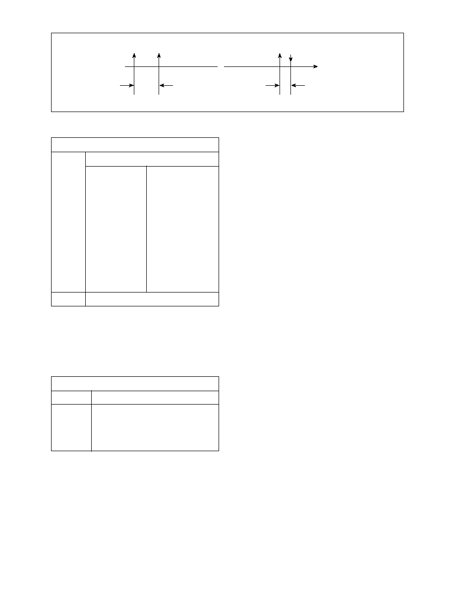
28
GP1020
STAT_CHK_SEL Write Address C5
H
Register bit mapping
Description
Signal source
Bit
selection with the
Selected input port
following encoding:
Bit 3 2 1 0
3 to 0
0 0 0 0
0
0 0 0 1
1
0 0 1 0
2
0 0 1 1
3
0 1 0 0
4
0 1 0 1
5
0 1 1 0
6
0 1 1 1
7
1 X 0 0
8
1 X 0 1
9
1 X 1 0
Self test signal
1 X 1 1
Ground
15 to 4
Not used, don't care.
REGISTER DESCRIPTION
STAT_CHK_SEL can be written into at any time. The SELF
TEST SIGNAL is both the sign and magnitude outputs (TSIGN
and TMAG output pins) of the SELF_TEST_GENERATOR
block and are connected internally.
STAT_CHK_SIGN and STAT_CHK_MAG
Read Addresses C5 and C6
H
Register bit mapping
Bit
Description
13 to 0
Unsigned integer ranging from 0 to 16383
representing the number of sign or
magnitude bits sampled during two
interrupt time base periods.
15 to 14
Don't care, held LOW.
These registers are overwrite protected. The overwrite
protection is released and the NEW_STAT_DATA bit of the
ACCUM_STATUS_A is reset on the trailing edge of a read to
STAT_CHK_MAG or a write operation to ALL_ACCUM_RESET
location. Therefore, STAT_CHK_MAG should be read after
STAT_CHK_SIGN.
For the first time the flag NEW_STAT_DATA is set after a
master reset, if a write to the STAT_CHK_SEL register has not
been performed within two interrupt time base (INT) periods,
non valid data will be latched in STAT_CHK_SIGN and
STAT_CHK_MAG registers. For this reason perform a dummy
read to STAT_CHK_MAG in order to clear the flag and wait for
the next time the flag is set to get valid data.
NOTE: the STAT_CHK_MAG register contains the number
of samples having the values 13 or23, and the STAT_CHK_SIGN
register contains the number of positive samples (1 or 3) from the
selected input port.
STATUS_LATCH WriteAddress 80
H
A write to this location with don't care data latches the state
of all status bits contained in ACCUM_STATUS_A,
ACCUM_STATUS_B, MEAS_STATUS_A and
MEAS_STATUS_B. Performing a write to STATUS_LATCH
prior to reading the status registers ensures reading of stable
status values. The latch takes effect within 200 nanoseconds of
the leading edge of the write pulse. The LOW to HIGH transition
of the INT signal will also latch the state of the status bit, thus it
is not necessary to write to STATUS_LATCH when the status
registers are to be read as a response to the INT signal in an
interrupt handling routine. The write to STATUS_LATCH is
required only when the status registers are read at `random'
times, controlled by the microprocessor. These two mecha-
nisms are mutually exclusive and should not be used in conjunc-
tion - if they are both used (a write to STATUS_LATCH after the
occurance of an INT signal) contentions and confusion will result.
To avoid this, make sure a read access does not take
place at the same time as an interrupt rising edge.
If the INT_MASKB bit in TIMER_CNTL register is not set to
HIGH, the interrupt will not latch the status bits in the status
registers ACCUM_STATUS_A, ACCUM_STATUS_B,
MEAS_STATUS_A and MEAS_STATUS_B but a
STATUS_LATCH write access will do so. Also, when a GP1020
is configured as a slave, it should have the INT_SOURCE and
the INT_MASKB bits in the TIMER_CNTL register set to HIGH
to get the status bits sampled at the same instant in both master
and slave GP1020s.
TDATA_DUTY_CYCLE Write Address C8
H
This register is associated with the
SELF_TEST_GENERATOR. It allows selection of the duty
cycle of the data inversion function.
The time base period is 11 C/A code chips. The value of
TDATA_DUTY_CYCLE, valid from 0 to 10, determines the
number of chips within the time base period where the data bit
modulating the self test signal will be inverted. When the self test
signal is fed back in a tracking channel, the inversion causes a
slope reversal in the accumulator of the Accumulate and Dump
module and prevents the accumulator from saturating over a
code epoch when TDATA_DUTY_CYCLE is properly set. This
is the same effect as noise on a real satellite signal.
REGISTER OPERATION
This register is a write only register and can be written into at
any time. At power up the register is reset, so it will always select
the data inversion function. If the bits are all 1 the data inversion
RTC_INT
TIME
Fig. 16
NEXT 2∑275
µ
s CLOCK EDGE
(FREE RUNNING)
UP TO 2∑275
µ
s DELAY
MAKES COUNT TOO HIGH
PREVIOUS 2∑275
µ
s
CLOCK EDGE
TIC
UP TO 2∑275
µ
s
DELAY MAKES
COUNT TOO
SMALL

GP1020
29
function will never be selected. For standard operation a single
0 is required and all the other bits must be at 1. The position of
the 0 in the register allows the duty cycle of the data inversion
function to be set as shown below:
Bits 10 9 8 7 6 5 4 3 2 1 0 Description
0 0 0 0 0 0 0 0 0 0 0 Power up condition, the
data inversion function
is always selected.
1 1 1 1 1 1 1 1 1 1 0 The data inversion
function is always
selected.
1 1 1 1 1 1 1 1 1 0 1 The data inversion
function is selected 10
times in 11.
1 1 1 1 1 1 1 1 0 1 1 The data inversion
function is selected 9
times in 11.
0 1 1 1 1 1 1 1 1 1 1 The data inversion
function is selected 1
time in 11.
1 1 1 1 1 1 1 1 1 1 1 The data inversion
function is never
selected.
TIMER_CNTL Write Address C2
H
Register bit mapping
Bit
Name
Description
0
TIC_PERIOD
When LOW, the TIC period is
175 ns3571,428 = 99∑9999ms.
When HIGH, the TIC period is
175 ns 3 51,948 = 9∑0909ms.
TIC_PERIOD is set LOW by
reset.
1
INT_MASKB
When LOW, the interrupt output
signal is disabled, the INT OUT
pin is held LOW and the status
bits are not sampled by an on-
chip or an externally generated
interrupt. When HIGH, the int-
errupt output signal is enabled
and the status bits will be
sampled by an interrupt.
INT_MASK is set LOW by
reset.
2
TIC_SOURCE
When LOW, TIC source is
internal, when HIGH, TIC
source is external (provided by
a companion GP1020 through
TICIN pin). TIC_SOURCE is
set LOW by reset.
Register bit mapping
Bit
Name
Description
3
INT_SOURCE
When LOW, the signal used to
latch the state of status bits and
the results of the STAT_CHECK
block is the positive edge in Intel
mode or the negative edge
in Motorola mode of the
INT signal generated on-chip.
When HIGH, the edge
of the INT signal provided on
INTIN pin of the device by a
companion GP1020 is used
instead. INT_SOURCE is set
LOW by reset.
4
TEST_OP/MARKB
When LOW, the GP1020
MARK output pin will output
the time MARK output. When
HIGH, the output will be driven
by a signal selected by the
CH1_DUMP/OSC_CHECK
bit (bit 8) of this
TIMER_CNTL register.
TEST_OP/MARKB is set
LOW by reset.
7 to 5
Mark Feedback active edge
selection, with the following
encoding:
Bit
Selected
7 6 5
function
0 0 0
FB1
0 0 1
FB1
0 1 0
FB2
0 1 1
FB2
1 0 0
FB3
1 0 1
FB3
1 1 0
TICOUT
1 1 1
TICOUT
The FBx
(rising edge) and
FBx
(falling edge) signal edges
are used to calculate the
pulse width of the Mark
Feedback signal. This calcula-
tion allows monitoring of the
pulse width and verification
that the result is in accordance
with the 1 ms
±
0.01 ms
specification. The TIC OUT
signal is also available as
feedback for test purposes.
Bits 7 to 5 are set LOW
by reset.

30
GP1020
Register bit mapping
Bit
Name
Description
8
CH1_DUMP/OSC
When LOW the GP1020
MARK output pin will
output a square wave with a
period of 4∑55 microseconds.
(40MHz/182). Because this
clock is derived from the
TCXO, its stability and
accuracy is representative of
the TCXO stability and
accuracy. When HIGH, the
GP1020 MARK output pin will
output a square-wave chang-
ing its level at each DUMP
event in channel 1. These
features are used for test
purposes during ATP of the
GPS sensor unit and the
TEST_OP/MARK bit (bit 4)
must be set to HIGH to get
either of these two test
outputs.CH1_DUMP/
OSC_CHECK is set LOW by
reset.
12 to 9
Interrupt time base selection
with the encoding given in the
following table.
Bit
12
11
10
9
Selected interrupt
High time
Low time
timebase period (
µ
s)
(
µ
s)
(
µ
s)
0
0
X
X
505.050
252.525
252.525
0
1
0
0
420.875
84.175
336.700
0
1
0
1
505.050
252.525
252.525
0
1
1
0
589.225
336.700
252.525
0
1
1
1
673.400
336.700
336.700
1
0
0
0
757.575
420.875
336.700
1
0
0
1
841.750
420.875
420.875
1
0
1
0
925.925
505.050
420.875
1
0
1
1
1010.100
84.175
925.925
1
1
0
0
1094.275
168.350
925.925
1
1
0
1
1178.450
84.175
1094.275
1
1
1
0
1262.625
168.350
1094.275
1
1
1
1
1346.800
420.875
925.925
Bits 12 to 9 are set LOW by reset.
_CHECK

GP1020
31
DETAILED OPERATION OF THE GP1020
1. MASTER RESET - Hardware or Software.
At Master Reset, all registers, accumulators and counters are
cleared except CHx_CNTL. In particular, this implies the follow-
ing initial states:
∑
All CHx_RSTB bits of the RESET_CNTL register are cleared.
Thus all tracking channel clock phases are disabled. Program-
ming registers can take place either before or after releasing the
CHx_RSTB bits.
∑
All the tracking channels are in UPDATE mode, the satellite
code selected is GPS PRN No. 17 and the EARLY code is
selected on the dithering arm. All CHx_CNTL registers are in
MODE 1.
∑
The TIC generator will be free running at start-up with a
100ms TIC period setting. The INT_MASKB bit of the
TIMER_CNTL register is LOW, therefore the INT_OUT signal
will be disabled and the output pin held LOW. The interrupt time
base is set to 505.05
µ
s.
∑
The BITECNTL bit of the BITE register is reset LOW (inactive
state). The associated BITECNTL output pin is also LOW.
∑
The data bus is forced into input mode to avoid contention at
power up.
2. SEARCH OPERATION at Power up, after a power
glitch, or after losing satellite signals.
REGISTER INITIALISATION
For each channel, the proper GPS or GLONASS signal
source has to be selected by writing the proper code into
CHx_SIG_SEL registers. The contents of these registers can be
changed at any time during the operation to change the signal
sources for any channels.
At power up, all CHx_RSTB bits of the RST_CNTL register
are in the reset LOW state. As stated above, in that state, all
tracking channel control registers can be programmed.
When it is required to perform a SEARCH for one satellite with
more than one channel, these channels are first reset if not
already in that state, with the corresponding CHx_RSTB bits,
then the control registers are programmed. In particular, each
CODE_SLEW register is programmed with a different value.
Then, the CHx_RSTB bits are released, causing the channels to
start operating at the same time with the same code phase. One
millisecond later, all channels will get the same accumulated
data and will be slewed with the pre-programmed values and will
continue with a known relative code phase difference. Note that
every time CHx_RSTB is set LOW, the code generator is reset.
The following additional initialisation operations have to be
performed. The block write addresses can be used whenever
appropriate.
CARRIER_DCO PROGRAMMING
The CARR_INCR_HI and the CARR_INCR_LO registers are
programmed in sequence with the relevant data according to the
estimated DOPPLER shift for the frequency bin being looked at.
The programming is effective as soon as the write operation to
CARR_INCR_LO is completed (In fact, a small delay of 175 ns
maximum will occur to allow synchronisation of the processor
write operation to the chip operation). If the content of
CARR_INCR_HI does not need to be modified, it is not neces-
sary to write into it. It is always necessary to write into
CARR_INCR_LO in order for the programming to be effective.
Note that, typically, the search algorithm would dwell on a given
frequency bin and perform a search over all code phases. Then
it would repeat the process for the next frequency bin.
CODE_DCO PROGRAMMING
The tracking channel being in UPDATE mode, the
PRESET_PHASE register does not need to be programmed.
The CODE_INCR_HI and the CODE_INCR_LO registers are
programmed in sequence with the relevant data according to the
estimated DOPPLER shift. Given that the CHx_RSTB bit of the
RESET_CNTL register is inactive, the programming is effective
as soon as the write operation to CODE_INCR_LO is completed.
If the content of CODE_INCR_HI does not need to be modified,
it is not necessary to write into it. It is always necessary to write
into CODE_INCR_LO in order for the programming to be effec-
tive.
CODE GENERATOR PROGRAMMING
1. Select in CHx_CNTL register the type of code to be used in
the dithering arm of the correlator; normally, for a search opera-
tion, either an early or a late code is selected. The PRESET/
UPDB bit will be set LOW, for example, in UPDATE mode by
master reset.
2. Select in CHx_CNTL register the code to be generated among
the 45 possible C/A codes or the unique GLONASS code.
(Actually, all possible code combinations are programmable
even those not used by the GPS constellation and some
GLONASS-like codes are also available.) The selected code is
applicable to both the prompt and the dithering arm.
3. Program each tracking channel CODE_SLEW register with
the desired code phase. The slew operation will become effec-
tive at the first dump e.g. about 1 ms after CHx_RSTB release.
The first dump will generate don't care accumulated data and will
set the associated CHx_NEW_ACCUM_DATA status bit. The
second and the following dumps will generate useful data.
4. Release the relevant CHx_RSTB bits of the RESET_CNTL
register in order to start operation of the tracking channels. When
channels of more than one GP1020 are being used to search for
the same code, consecutive write operations to each chip's
RESET_CNTL register should ensure a startup with reasonably
well known relative code phases between the two chips.
Whenever the code clock is being inhibited (to slew the code
phase), the Accumulate & Dump module is held reset. It will start
to accumulate correlation results only after the slew operation is
completed.
3. READING the ACCUMULATED Data
Every time a DUMP occurs, the corresponding
CHx_NEW_ACCUM_DATA status bit is set in the
ACCUM_STATUS_A register. All In-phase and Quad-phase
registers together with ACCUM_STATUS_A and
ACCUM_STATUS_B registers are mapped in consecutive ad-
dresses so that they can be block-read after every timebase
interrupt. Alternatively, a polling technique can be used by
periodically reading the ACCUM_STATUS_A register to find if
an interrupt or a write into STATUS_LATCH has been per-
formed.
The data contained in the IN_PHASE and QUAD_PHASE
registers of the prompt and dithering arms will be protected from
an overwrite due to consecutive DUMP events. The protection
mechanism is released on the trailing edge of a read operation
of the Q_PROMPT register. Thus the order of reading I_DITH,
Q_DITH and I_PROMPT is optional but Q_PROMPT must
always be read last to ensure coherence of the data set and to
release the overwrite protection mechanism.
The CHx_MISSED_ACCUM bit of the ACCUM_STATUS_B
register indicates new accumulated data has been missed
because of a too long response time for reading the accumulated
data. This status bit, when set, is latched until it is cleared by a
write operation to CHx_ACCUM_RESET or by a master reset or
by CHx_RSTB set to LOW.
4. SEARCH on other CODE PHASES
When it is desired to correlate on the next code phase, the
CODE_SLEW has to be programmed with a value of 2 (in units

32
GP1020
of half code chips). The slew will be effective on the next dump.
Thus this dump will generate don't care accumulated data and
as a minimum, the Q_PROMPT register will have to be read to
release the overwrite protection mechanism.
Note that it is only possible to delay the phase of the code. It
cannot be advanced.
5. DATA BIT SYNCHRONISATION Related
Operations
When the right code phase is found, the carrier loop is closed.
The CARR_INCR_HI and CARR_INCR_LO registers can be
reprogrammed at any time to close the feedback loop and
resume code tracking.
The Data Bit Sync algorithm should find the data bit transition
instant. The processor calculates the present one millisecond
epoch and programs this value into the 1MS_EPOCH register.
The effect is immediate.
After each DUMP, the epoch counter value can be read within
1ms and preferably at the same time as the integrate and dump
registers. This provides a means of verifying that the epoch
counters are indeed properly programmed. Programming the
epoch counter in the 500
µ
s period following a valid
CHx_NEW_ACCUM_DATA should ensure that the program-
ming becomes effective before the next DUMP.
Alternatively, the EPOCH registers can be left free-running
and the delta-epoch can be added by the software each time it
reads the EPOCH registers. However, the dithering between
early and late code will be controlled by the actual contents of the
EPOCH registers, which will not necessarily be in phase with
data bit boundaries.
6. READING the MEASUREMENT Data
At every occurrence of a TIC, the measurement data is
latched in measurement data registers. The TIC does not
generate any interrupt signal, however, it does set the
CHx_NEW_MEAS_DATA status bits of the MEAS_STATUS_A
register. This register is normally always read while collecting
accumulated data once every 505.05 microseconds (The INT
OUT signal rate). The software tests the
CHx_NEW_MEAS_DATA status bits to determine if new meas-
urement data is available to be read. For each channel, the last
measurement data register to be read must be
CHx_CARR_CYCLE because the trailing edge of this read
releases the overwrite protection mechanism and clears the
corresponding CHx_NEW_MEAS_DATA bit. The software
must also read the MEAS_STATUS_B register to determine if
there was any missed measurement data or if phase and epoch
counters were being slewed during the last TIC period, indicating
invalid measurement data for the affected channel.
7. The PRESET Mode
Each tracking channel can be individually programmed to
operate either in UPDATE or PRESET mode. A given channel
is programmed in PRESET mode by writing a HIGH into the
PRESET/UPDB bit of the CHx_CNTL register.
The sequence of operations is as follows:
1. Write into CHx_CNTL to select the PRESET mode together
with the appropriate code, code format on the dithering arm, etc.
Since the PRESET mode is selected, the new selected code and
code format will be effective on the next TIC.
2. Between the instant at which the PRESET mode is selected
and the next TIC, the tracking channel will continue to operate
normally, that is, it will provide accumulated data for the signal
being tracked.
3. The INCRement registers of the CODE and CARRIER DCO'S
have to be loaded with the appropriate frequencies for the new
signal to be tracked either immediately or only after the TIC has
occured if it is desired not to disturb the tracking in effect.
4. Load the following PRESET registers:
PRESET_PHASE: Will set the code DCO phase.
CODE_SLEW: Will set the code phase.
1MS_EPOCH: Will set the 1 ms epoch.
20MS_EPOCH:Will set the 20 ms epoch.
It is important to have the PRESET mode selected prior to
programming the CODE_SLEW and the EPOCH registers in
order to have these new values effective on the next TIC as
opposed to immediately if they were programmed under UP-
DATE mode.The PRESET_PHASE register can be programmed
either before or after selecting the UPDATE mode. In PRESET
mode the value to program in the CODE_SLEW register repre-
sents the delay between the TIC and the first code chip.
To ensure correct PRESET of EPOCH counters, the loading
of PRESET registers has to be completed prior to the TIC relative
to which the PRESET values are computed. Thus the operation
has to take place within a TIC window.
It is important to load the 20MS_EPOCH register last in the
loading sequence. The trailing edge of a write to this register
enables the PRESET operation on the next TIC.
5. After the PRESET operation has taken place on a TIC, the
PRESET/UPDB bit of the CNTL register is reset and the channel
goes back to UPDATE mode. It is possible that the code phase
has to be slewed so the CODE_SLEW register when loaded will
then cause a slew to start on the next DUMP.
On the TIC, the measurement data saved for the signal being
tracked so far will be valid. The measurement data registers (or
at least CHx_CARRIER_CYCLE register) must either be read or
a write operation to CHx_MEAS_RESET must be made in order
to clear the measurement status bits and allow measurement
data acquisition on the next TIC for the new signal to be tracked
under PRESET mode.
8. The TIC GENERATOR and the Interrupt Time
Base
The interrupt time base consists of a free-running counter
providing a pulse of constant period on a GP1020 output pin. The
frequency uncertainty on this time base will be identical to the
system oscillator drift. The interrupt time base shares some
dividers with the TIC generator. The period of this time base is
175ns 3 2886 = 505.05
µ
s at power up, but may be changed by
programming TIMER_CNTL register, and is always an exact
sub-multiple of the TIC time base. Every 198th (or 18th) interrupt
pulse at default rate will occur at the same time as a 100ms (or
9.0909ms) TIC, not taking into account propagation delays.
Either INT IN or INT OUT (as controlled by the INT_SOURCE bit
of the TIMER_CNTL register) is used to sample and latch the
status bits and statistics on incoming sign and magnitude bits.
The interrupt is maskable. The INT_MASKB bit of the
TIMER_CNTL register when set LOW forces the logic level on
the output pin to LOW. A master reset will set this bit LOW.
9. SIGNAL PATH DELAY Introduced by Hardware
Signal Processing
The signal path delay has two components as follows:
D
t
= Total path delay = D
a
+ D
d
D
a
= Analogue path delay; varies with temperature and
component tolerances.
D
d
= Digital path delay; constant if oscillator drift
variations are neglected.
For GPS signals, D
d
= 125ns. This delay is the time from the
sampling edge of the SIGN and MAG bits in the GP1010 (SAMP
CLK) to the performance of the correlation in the GP1020 on these
same SIGN and MAG bits (100ns) plus the delay between the
correlation and the TIC clock phases in the master GP1020 (25ns).

GP1020
33
RTC_INT AT 1 SEC RATE
REAL TIME
CLOCK
CLOCK (439∑56kHz)
COUNTER
RESET
ENABLE
NOTES
1. Latch counter value
saved on TIC.
2. Register read with
measurement data.
100ms TIC
Fig. 17 RTC block diagram
MICROPROCESSOR
SYSTEM
RTC_DELAY
GP1020
10. Short Glitch Recovery
Refer to the block diagram shown in Fig. 17 for the following
discussion.
It is assumed that the RTC selected provides an interrupt
output signal which occurs periodically, every 100ms or every
second. The interrupt is sent to both the GP1020 and the
processor system. Within the GP1020, the interrupt is connected
to the RTC_INT input pin of the GP1020. Its edge enables the
RTC_DELAY counter. This counter is clocked by a signal with a
period of 2.275
µ
s and increments until the next TIC. The TIC
causes the value of RTC_DELAY to be latched in order to be
read with the measurement data.
When the processor receives the RTC interrupt, it reads the RTC
time. Alternatively, RTC_TIC may not be routed to the processor, but
instead, every time the RTC_TIC_ACK status bit of
MEAS_STATUS_B is set in the GP1020, the software reads the
RTC time. With this information, together with the contents of
RTC_DELAY, the software is able to determine first the delay
between the RTC and the system clock and secondly, with consecu-
tive readings, the RTC drift can be evaluated. These two pieces of
information are stored in non-volatile RAM every time they are
calculated. After occurrence of a power glitch, the 100ms_TIC
timebase restarts free running but with an arbitrary phase relation-
ship with respect to the TICs before the power glitch. The RTC
interrupt process occurs again as described above and it is possible
to relate the new system TIC time relative to the previous. Ideally, this
process is precise enough such that the data bit sync is not lost and
all the channel control registers can be reprogrammed with proper
values. Once the timing relationship is known, the PRESET mode
can be used to resume tracking of the signals.
If data bit synchronisation cannot be achieved on a given channel,
but proper code and carrier lock are obtained, the software should
jump to the data bit synchronisation algorithm. If lock is not obtained,
then the software should jump to the search algorithm. Given the
magnitude of error terms (summed) and the worst case error allowed
in order to keep data bit synchronisation, it is possible to calculate the
length of the longest permitted power glitch. See Fig. 20.
11. TIME MARK Generator
The Time Mark generator is designed to provide a one second
Time Mark output signal which can be synchronised with a given time
base, such as the receiver time base, the GPS time or UTC. The
Time Mark is generated after a certain programmable delay relative
to the TIC.
The architecture chosen (see Fig. 19) involves minimal
hardware being clocked at a high rate and so gives low power
consumption.
As an example, to synchronise TIME MARK to UTC, the software
could have the following sequence of operations (see Fig. 21):
1. Acquire measurement data at time to (on an arbitrary TIC)
2. Solve for UTC at measurement instant UTC (t
0
). Note that the
solution can only be accurate to within the hardware propa-
gation delays in the receiver, typically a few microseconds,
unless these delays are calibrated and UTC solution is
corrected accordingly.
3. Compute on which 100ms TIC, t
m
, to take the next sample of
measurement data such that:
UTC TIME MARK 2 t
m
= d
1
1d
2
RTC_INT
Fig. 18 RTC timing diagram
RTC TIME READ HERE
BY PROCESSOR
POSITION FIX COMPUTED ON THIS TIC.
TIC IS GPS TIME TAGGED.
100ms TIC
RTC_DELAY
D
NOTES
1. D = delay between RTC timebase and system time t
s
.
2. Consecutive measurements of D give an indication of RTC drift.
3. Resolution of D is a function of input clock to RTC_DELAY counter.
t
s
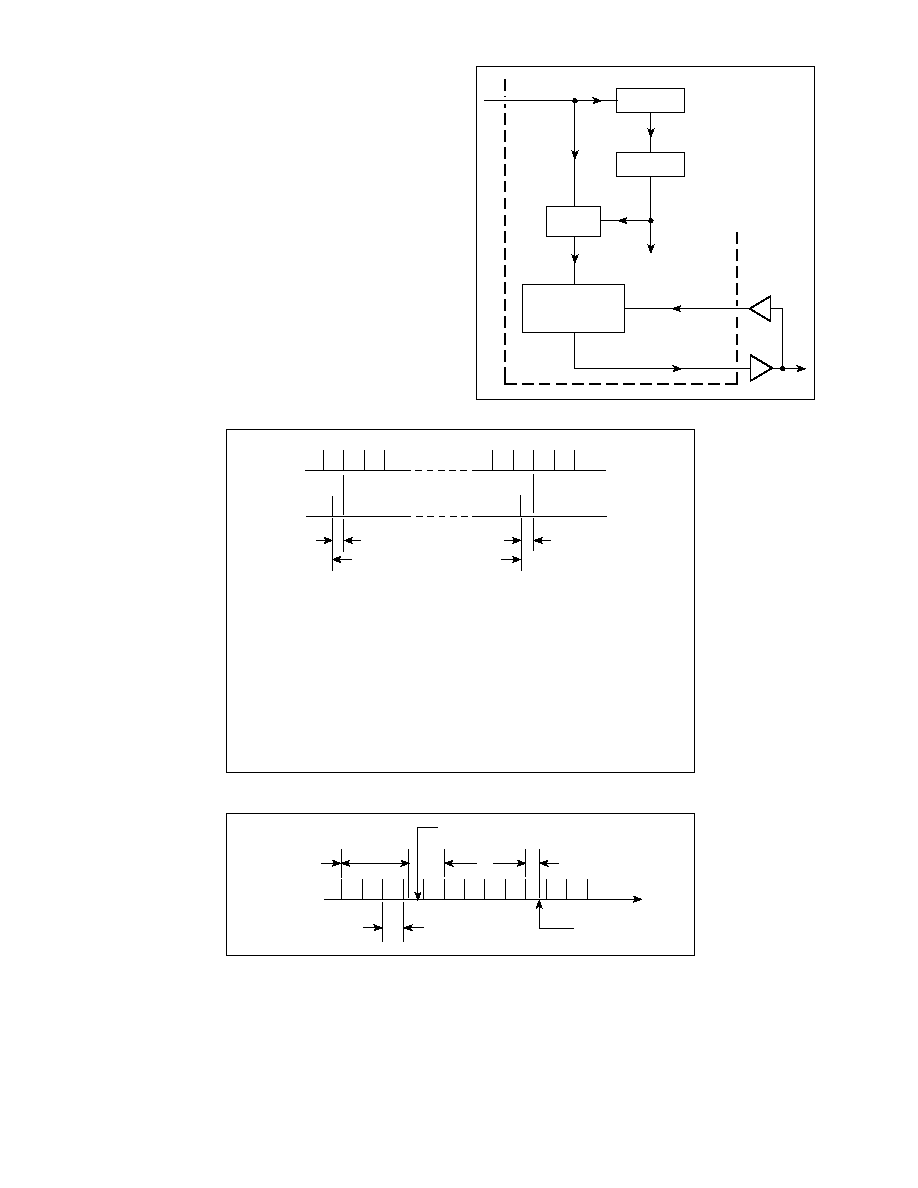
34
GP1020
Where UTCTIME MARK = Desired time mark synchronised to
a UTC second.
d
1
= k 3 (time between TICS),
where k=INTEGER and d
1
>Nav solution computation
delay.
d
2
= time offset (with 50 ns resolution) between time
mark and 100ms_TIC labelled t
r
d
2
< (time between TICS)
4.
∑
Acquire measurement data at t
m
∑
Compute Nav solution at t
m
∑
Propagate Nav solution at UTC
∑
Given the oscillator drift, the delay of 25 ns added by
TIME_MARK_GEN block and the calibrated propagation
delay, compute DOWN_COUNT, the value to program into
the programmable down counter to delay the time mark by d
2
.
5. Program down counter with DOWN_COUNT before the
occurrence of t
r
.
6. Output ARINC Data within 200ms after t
r
(following ARINC
743)
7. Locate t
m
1
1 and go back to step 4.
CLOCK
GENERATOR
4
571, 428
40MHz MASTERCLOCK
20-BIT
PROGRAMMABLE
DOWN COUNTER
20-BIT
COUNTER
CONTROL
LOGIC
CNTL
100ms TIC
Fig. 19 Block diagram of TIME MARK generator
4
7
CLK
MARKFBx
1 SEC. TIME MARK
EXTERNAL
LINE
DRIVERS
GP1020
RTC TIC
Fig. 20 Timing diagram of a short glitch
100ms TIC
D
1
D
RTC = (RTC
2
2
RTC
1
2
RTC
DRIFT
)
NOTES
1. t
s2
= t
s1
2
D
1
1D
RTC1D
2
(
±
error terms)
2. ERROR TERMS: in ts
1
: Equal to error terms of GPS time computation
while getting the NAV solution
in D
1
: Can be too long or too short by r,
where r = RTC_DELAY counter clock period
in D
2
: Same as D
1
in DRTC : Residual error in RTC drift estimate,
= (effective RTC
DRIFT
)2(estimated RTC
DRIFT
)
t
s1
t
s2
t
s3
RTC
1
RTC
2
D
2
NAV SOLUTION
COMPUTATION
DELAY
Fig. 21 TIME MARK timing diagram
100ms TIC
t
0
t
r
d
1
COMPUTE
t
m
d
2
t
m
TIME BETWEEN TICs
IS CONSTANT
OUTPUT
UTC TIME MARK
TIME

GP1020
35
Fig. 22 Integrated carrier phase measurement
TIC
0
TIC
1
TIC
2
Y
0
2
p
2
Y
0
K
1
CYCLES
D
Y
1
Y
1
K
2
CYCLES
D
Y
2
Y
2
1. Reading at TIC
0
:
2. Reading at TIC
1
:
3. Reading at TIC
2
:
CHx_CARR_DCO_PHASE
0
= Y
0
CHx_CARR_CYCLE
0
CLEARED
CHx_CARR_DCO_PHASE
1
=Y
1
CHx_CARR_CYCLE
1
= K
1
1
1
CHx_CARR_DCO_PHASE
2
= Y
2
CHx_CARR_CYCLE
2
= K
2
1
1
D
Y
1
= 2
p
(K
1
1
1) 1Y
1
2
Y
0
= 2
p
(CHx_CARR_CYCLE
1
)1CHx_CARR_DCO_PHASE
1
2CHx_CARR_DCO_PHASE
0
SD
Y = 2
pS
(CHx_CARR_CYCLE)1CHx_CARR_DCO_PHASE
LAST
2CHx_CARR_DCO_PHASE
0
CARRIER CYCLES MEASUREMENT
OVER MORE THAN ONE TIC PERIOD
UTC ERROR BUDGET
The following error budget is associated with the generation
of the Time Mark:
Total Error =
TDOP1Clock Resolution1Oscillator Drift Residual Error.
1
Computation induced Error.
1
Time mark transfer delay through Drivers/cables.
1
Propagation delay in hardware, from antenna to
correlator to measurement data sampler, where
typical values are:
1. TDOP: estimated at 177ns with S/A ON (2 s number)
2. Clock Resolution: 50ns (in 21 bit programmable down
counter).
3. Oscillator Drift Residual Error:
(a)
Due to temperature change on
TCXO since last oscillator drift
computation: about 50ns, computed
with the following assumptions:
(i) TCXO max slope is
±
1 ppm/
∞
C
(ii) Temperature max variation is 5
∞
C/minute
(iii) The oscillator drift is computed every
second and is at most one second old at UTC
time mark.
For example:
1ppm/
∞
C 3 5
∞
C/min 3 1sec
= 83ns for a temperature step change
or 41.5 ns (rounded to 50ns) for a linear ramp
(b)
Due to bias in drift estimation about 50ns max (rough
guess)
TOTAL oscillator drift error = (a) 1 (b)
100ns.
4. Computation induced error: It is assumed that enough
significant bits are retained such that this error approximates
zero.
5. TIME MARK transfer delay through drivers/cables: This
will be calibrated and compensated for up to the GPS receiver's
output using the feedback to the down counter. There will be a
residual error due to:
(a) Clock resolution = 50ns
(b) Feedback delay calibration = 25ns (estimated)
6. Propagation delays in the hardware: These are estimated
to be in the range of a few microseconds and are therefore the
major contributor to the TIME MARK synchronisation error. An
estimate could be included in the software to improve total
accuracy when the total hardware design is complete.
TOTAL = 177ns150ns1100ns10175ns1hardware delays
TOTAL = 402ns1hardware delays.
12. INTEGRATED CARRIER PHASE measurement
The GP1020 tracking channel hardware allows measure-
ment of integrated carrier phase through CHx_CARR_CYCLE
and CHx_CARR_DCO_PHASE registers. These two registers
are part of the measurement data sampled every TIC. The first
one contains the 16 more significant bits of the number of full
cycles elapsed and the second one contains the two remaining
less significant bits plus the cycle fraction (phase). Fig. 22 shows
how to add consecutive readings of these registers over several
TICs in order to get a consistent integrated carrier phase.

36
GP1020
The next table contains the truth table of the weight converter
used in the SELF_TEST_GENERATOR :
CARRIER_DCO bits
MAG
SIGN
(MSB-LSB)
01011
1
MSB
011xx
1
MSB
100xx
1
MSB
10100
1
MSB
All other combinations
0 MSB
The design of the weight converter will drive a HIGH on the
SIGN bit for 50% of the time and on the MAG bit for 31% of the
time.
Examples 1 and 2 show the results of the five first accumula-
tions of the accumulated data for two different settings of the
SELF_TEST_GENERATOR and the channels. Because the
channels had been started at the same time, they are practically
in phase with the incoming data (Sign and Mag outputs of the
SELF_TEST_GENERATOR).
13. BUILT-IN TEST Functions
A. CHIP LEVEL Built-in Test Functions
SELF_TEST_GENERATOR
The GP1020 provides an on-chip self-test pattern generator
which is switched on under software control by setting
SELF_TEST_EN bit of the BITE register. It uses tracking chan-
nel 1 or 2 according to the setting of SELF_TEST_SOURCE bit
of the BITE register to generate SIGN and MAGNITUDE -like
signals which can be fed back to any or all other channels by
selecting the self test signal source in CHx_SIG_SEL. The self-
test signal has a fixed data bit pattern of alternating one and zero
every 20 milliseconds, the first bit being LOW. It has a fixed noise
pattern which corresponds to particular In-phase and Quad-
phase accumulated values. The C/A code and the Doppler shift
can be varied by programming the relevant registers of the
channel which has been selected by SELF_TEST_SOURCE.
The standard software can then be used to acquire and track the
self-test signal but it should take into account the fact that this
self-test signal is not a real GPS signal.
The SELF_TEST_GENERATOR output signal can also be
wrapped around externally by connecting the TSIGN and TMAG
output pins to a GPS or GLONASS input port. Normally, the test
source and tested channels will have the same DCO settings.
Example 1:
Register settings
Value
Comments
(Hex)
BITE
0020
STG on, CH1 as source
TDATA_DUTY_CYCLE
0000
No noise (will cause an overflow
condition in Q_PROMPT register
if signals are in phase)
CHx_SIG_SEL
000A
Signal from the STG
CHx_CODE_INCR_HI
016E
CHx_CODE_INCR_LO
A4A8
CHx_CARR_INCR_HI
01F5
CHx_CARR_INCR_LO
C28F
CHx_CNTL
0225
SV PRN 19, Dithering code
RESET_CNTL
007F
Start all channels at the same time
Results
First
Second
Third
Fourth
Fifth
dump
dump
dump
dump
dump
CHx_I_DITH
0388
0318
016C
04CC
02AC
CHx_Q_DITH
3D28
3D98
3C34
3D78
3FE4
CHx_I_PROMPT
0A30
093C
0930
08F8
0978
CHx_Q_PROMPT
7FFC
7FFC
7FFC
7FFC
7FFC
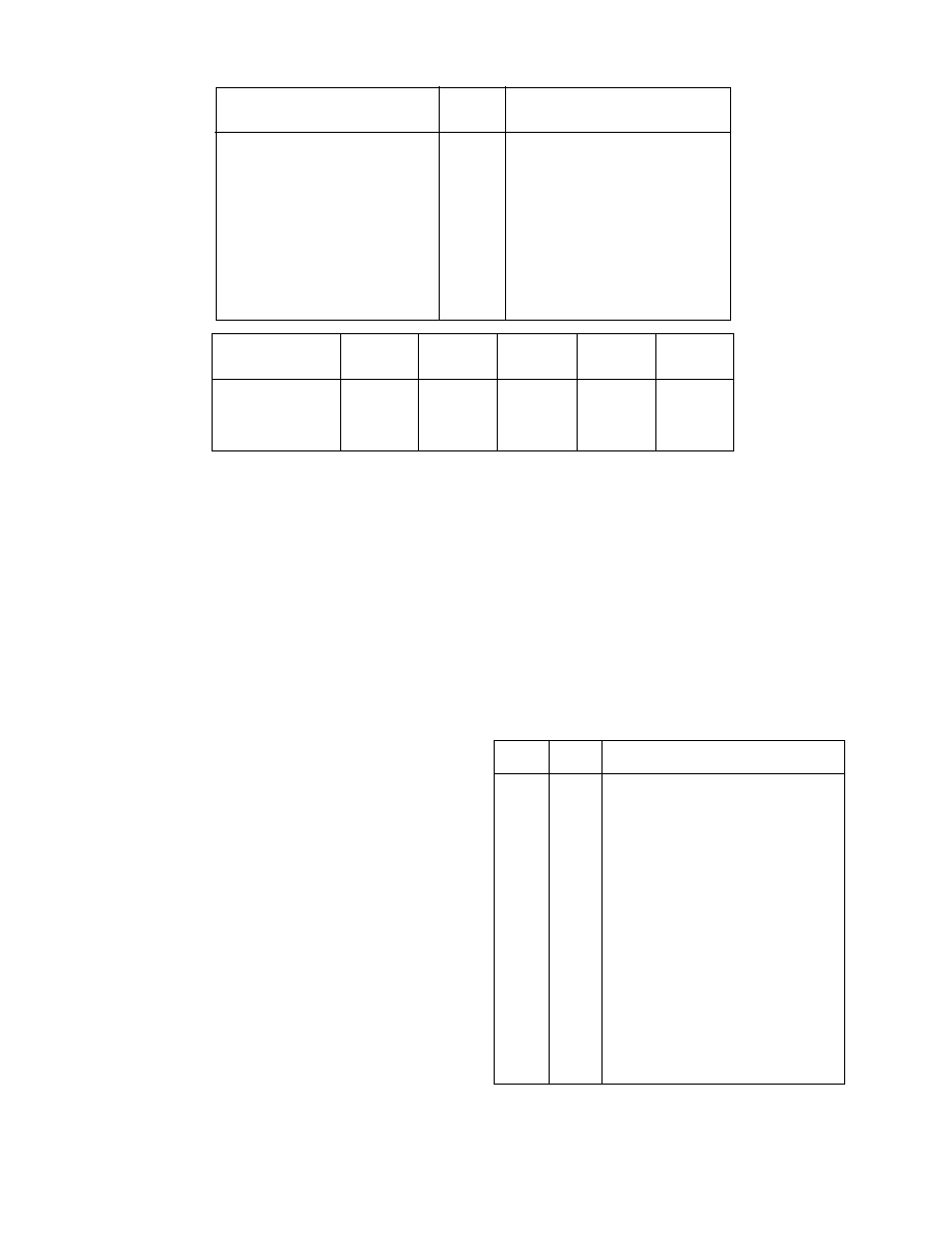
GP1020
37
Scan Loops and Internal Node Real-Time Observability
A number of registers are not connected to the data bus in any
way. These registers have two modes of operation: The normal
mode and the SCAN LOOP mode in which the flip flops are cascaded
to form a shift register. There is one such scan loop per channel.
Fig. 23 shows a block diagram of the Chip test functions. TDI1
(Test Data In) is a serial input common to all scan loop shift registers.
Each scan loop has a separate data O/P pin TDO (1:7) (Test Data
Out).
The control signal TSCAN (Test Scan) determines whether the
registers operate in normal mode (TSCAN LOW) or in scan loop
mode (TSCAN HIGH).
The Control Signal TCKS (Test Clock Select), when HIGH,
selects the 7 test clocks TCK(1:7) as a replacement for the seven
clock phases provided by the clock generator in normal mode. This
is intended for use only in the device factory and not in normal
operational use. TMS1 and TMS2 are Test Mode Select control pins.
Their function is detailed in the following table:
TMS2
TMS1
LOW
LOW
Normal mode: SIGN (2:8) and
MAG (2:9) configured as inputs.
TDO (1:7) held LOW. TCK(1:7)
configured as inputs. SIGN (9) is
always used as a normal input.
LOW
HIGH
Scan Loop mode: SIGN (2:8)
and MAG (2:9) onfigured as
inputs. TDO (1:7) output serial
scan data. TCK (1:7) configured
as inputs.
HIGH
X
Channel 1 observability mode:
SIGN (2:8), MAG (2:9) and TCK
(1:7) configured as outputs and
together with TDO (1:7) allow
real-time observability of internal
nodes of channel 1 as listed
below. The internal TIC signal
and the signal latching the status
bits are also available on TDO4
and TDO7 pins.
Example 2:
Register settings
Value
Comments
(Hex)
BITE
0020
STG on, CH1 as source
TDATA_DUTY_CYCLE
07F7
Invert the data 8 times in 11
CHx_SIG_SEL
000A
Signal from the STG
CHx_CODE_INCR_HI
016E
CHx_CODE_INCR_LO
A4A8
CHx_CARR_INCR_HI
01F5
CHx_CARR_INCR_LO
B1B3
CHx_CNTL
0315
SV PRN 1, Early_Minus_Late code
RESET_CNTL
007F
Start all channels at the same time
Results
First
Second
Third
Fourth
Fifth
dump
dump
dump
dump
dump
CHx_I_DITH
2230
1EB8
2170
2030
1F00
CHx_Q_DITH
0598
0568
0374
078C
03CC
CHx_I_PROMPT
F8F4
0078
03E8
FF08
0590
CHx_Q_PROMPT
46D8
4798
4914
47B8
46D4
ADD_DAT_TST REGISTER
The ADD_DAT_TST register allows the software and the ATE
to verify the functionality of the data and address busses. For full
details see ADD_DAT_TST section of DETAILED DESCRIP-
TION OF REGISTERS.
B. SYSTEM-LEVEL Built-in Test Functions
GP1010 BITE interface:
The GP1020 BITE CNTL discrete output is provided to drive
the corresponding discrete input pin of the GP1010. When active,
this control unlocks the PLL and switches off the GP1010 front-
end amplifiers. As a result, the GP1020 should read an unlocked
status at its PLL LOCK discrete input.
The GP1020 includes Sign and Magnitude statistics checker
circuit.
GLONASS IC BITE interface:
Uses the same BITE CNTL discrete output to put the GLONASS
IC into test mode and one GP1020 discrete input pin,
GLONASSBIT, for GLONASS IC go/nogo status.
TIME MARK :
Three MARK FEEDBACK input pins, selected by bits 7 to 5 of
TIMER_CNTL, are provided for testing the signal outputs of
TIME MARK line drivers.
Also, software selectable control bits (TIMER_CNTL bits 4
and 8) allow multiplexing of the normal 1 second period TIME
MARK with one of two test signals, either 40MHz/91 =
439.5604KHz intended for oscillator drift measurement or
CH1_DUMP for system fault-finding purposes.
14. CHIP MANUFACTURING-TEST Functions
The GP1020 design incorporates a series of features to
increase (a) the observability of internal nodes when working in
the application and ( b) the observability and the controllability of
the circuit during chip-level testing during manufacture. The
following presents a summary of the chip test functions:
TEST REGISTERS
A number of registers have been added to improve the
testability of the chip. They are not required for normal
operation : CHx_TST_CODE_PHASE, CHx_TST_CYCLE and
CHx_TST_CODE_SLEW.
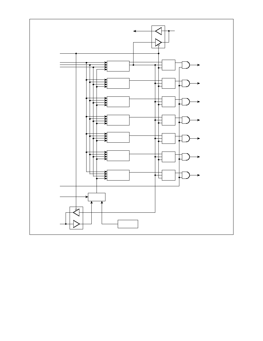
38
GP1020
OTHER CHIP
FUNCTIONS
CHANNEL 1
CHANNEL 2
CHANNEL 3
CHANNEL 4
CHANNEL 5
CHANNEL 6
CNTL MUX
TDI 1
TCK 8
TSCAN
SERIAL DATA
NODES
MUX
CNTL
MUX
CNTL
MUX
CNTL
MUX
CNTL
MUX
CNTL
MUX
CNTL
MUX
CNTL
CLOCK
GENERATOR
TMS 2
SIGN (2 : 8)
MAG (2 : 9)
TDO (1)
TDO (2)
TDO (3)
TDO (4)
TDO (5)
TDO (6)
TDO (7)
TMS1
TCKS
TCK (1 : 7)
TCKS
CLK (1 : 7)
CLK (1 : 7)
Fig. 23 Chip test functions

GP1020
39
TABLE OF ACCESSIBLE CHANNEL INTERNAL NODES
Prompt
bit 0
bit 1
bit 2
bit 3
TCK3
TCK4
TCK5
TCK6
CNTL PIN: TMS1:
CNTL PIN: SIGN9
O/P pin
SIGN 2
MAG 2
SIGN 3
MAG 3
SIGN4
MAG 4
SIGN 5
LOW
LOW
Prompt
bit 13
bit 11
bit 10
bit 9
bit 8
bit 7
bit 6
HIGH
LOW
Dithering
13
11
10
9
8
7
6
LOW
HIGH
Prompt
12
5
4
3
2
1
0
LOW
HIGH
Dithering
12
5
4
3
2
1
0
IN PHASE I & Q ACCUMULATOR ARM
MAG 5
SIGN 6
MAG 6
SIGN 7
MAG 7
SIGN 8
MAG 8
MAG 9
Prompt
bit 13
bit 11
bit 10
bit 9
bit 8
bit 7
bit 6
Dump
Dithering
13
11
10
9
8
7
6
Dump
Dithering
12
5
4
3
2
1
0
Dump
QUAD-PHASE I & Q ACCUMULATOR ARM
Prompt
12
5
4
3
2
1
0
Dump
MIX_CORREL output
Dithering
0
1
2
3
Dithering
0
1
2
3
In Phase ARM
Prompt
0
1
2
3
Quad Phase ARM
CNTL PIN: TMS1:
CNTL PIN: SIGN9
TDO1
TDO2
TDO3
TDO4
TDO5
TDO6
TDO7
CodeCLK
Prompt C/A code
Preset load
TIC
CARR DCO O/P bit 27
1ms epoch carry
STATUS latch control
Code CLK
Dithering C/A code
CARR DCO O/P bit 25
CARR DCO O/P bit 26
CARR DCO O/P bit 27
1ms epoch carry
STATUS latch control
LOW
X
HIGH
X
CNTL PIN: TMS1:
CNTL PIN: SIGN9
TCK1
TCK2
TCK7
Sampled SIGN
Sampled MAG
RESCODEGEN
X
X

40
GP1020
15. BOUNDARY SCAN LOOP
A boundary scan loop is implemented to allow the ATE to verify the connections of the chip at board level. The following pins are
not included in Boundary Scan Loop :
TDI1
100/219kHz
SAMPCLK
MASTERCLK
BIAS
PLLLOCKIN
SLAVECLK
TCK(1:8)
MARK
RTCINT
MARKFB1
MARKFB2
MARKFB3
NANDA
NANDB
NANDOP
The TAP controller has all functions necessary to be compatible with the JTAG standard (IEEE 1149.1-1990) with a few exceptions:
All bidirectional pins are in input mode when the TRST signal is inactive (HIGH)
so the chip cannot run freely when in bypass mode.
∑
The Capture-IR state loads the instruction 000 instead of x01.
∑
The pins TMS, TCK and TRST do not have pull-up resistors.
∑
This is the order of the pins in the loop (column by column):
A7
A8
MASTER/SLAVE
TCKS
MASTERRESET
MOT/INTEL
CS
WEN
RW
TMS2
TMS1
TMAG
*
TSIGN
*
MAG2
INTOUT
*
SIGN2
MAG3
SIGN3
MAG4
SIGN4
MAG5
SIGN5
MAG6
SIGN6
MAG7
SIGN7
MAG8
SIGN8
MAG9
SIGN9
MAG1
SIGN1
MAG0
SIGN0
CLKSEL
BITECNTL
*
GLONASSBIT
INTIN
TICIN
TICOUT
*
D0
D1
D2
D3
D4
D5
D6
D7
WPROG
D8
D9
D10
D11
D12
D13
D14
D15
ALE
A1
A2
A3
A4
A5
A6
TSCAN
NOTE: An asterisk in the above list indicates an output pin.

GP1020
41
APPLICATION NOTES
PCB LAYOUT CONSIDERATIONS
The GP1020 is a fast CMOS device so, although clock rates are low, the edge speeds can be very high. The board layout must,
therefore, handle these edges on both output signals and on power supply current.
SIMPLIFIED SYSTEM
It is not always necessary to use all of the features of the GP1020 to make a good GPS receiver. The following pin connections
show the minimum requirement and are given as a guide only.
Unused inputs must be tied to V
SS
or V
DD
and not left floating. Failure to observe this may result in malfunction or damage to
the device.
Pin No.
1 and 2
3
4 and 5
6
7
8
9
10
11
12
13
14 and 15
16 and17
18
19
20
21
22
23 to 39
40
41
42 and 43
44
45
46
47
48
49
50
51
52
53
54
55
56
57
58 to 65
66
67
68 and 69
70
71
72 and 73
74
75
76 and 77
78 and 79
80
Signal name
A7, A8
MASTER/SLAVE
TSCAN, TCKS
TDI1
MASTERRESET
MOT/INTEL
CS
V
SS
V
DD
WEN
RW
TMS2, TMS1
TMAG, TSIGN
MAG2
100/219kHz
V
DD
V
SS
INTOUT
SIGN and MAG 1 to 9
V
SS
V
DD
MAG0, SIGN0
SAMPCLK
V
DD
MASTERCLK
V
SS
BIAS
V
SS
V
DD
V
SS
CLKSEL
PLLLOCKIN
BITECNTL
GLONASSBIT
SLAVECLK
INTIN
TCK 1to 8
TICIN
TICOUT
D0 and D1
V
SS
V
DD
D2 and D3
TIMEMARK
RTCINT
MARKFB 1 and 2
D4 and D5
V
DD
Description
Address bus
Master or Slave mode select
Control Test mode
Test Data serial input
General reset, active low
Bus mode select
Chip Select, active low
Ground
Positive supply
Write Enable - see mode table, page 3
Read/Write - see mode table, page 3
Test Mode Select 2 and 1
Test PRN pattern output
Source 2 MAG input
Clock output
Positive supply
Ground
Interrupt output
Source 1 to 9 SIGN and MAG inputs
Ground
Positive supply
Source Mag and SIGN inputs
Sampling clock
Positive supply
40MHz Master Clock
Ground
Bias for Master Clock
Ground
Positive supply
Ground
100kHz (high)/219kHz (low) select
PLL Status input
BITE control to Front-end
GLONASS BITE input
Master to Slave clock
Interrupt input for Slave
Test clocks or signals
TIC input to Slave
TIC output from Master
Data bus
Ground
Positive supply
Data bus
1 PPS output
Real Time Clock interrupt input
Time Mark driver feedback
Data bus
Positive supply
Connection
To microprocessor
High, unless Slave
Both low
Low
Power-on timer
High for Motorola, low for Intel
To microprocessor
0V
1
5V
To microprocessor
To microprocessor
Both low
Leave open
Low
Leave open
1
5V
0V
To microprocessor
All low
0V
1
5V
To GP1010
To GP1010
1
5V
To GP1010
0V
See Fig. 12 (page 8)
0V
1
5V
0V
High
Low or GP1010
Leave open
Low
Leave open
Low
All low
Low
Leave open
To microprocessor
0V
1
5V
To microprocessor
Leave open
Low
Both low
To microprocessor
1
5V
Continued...

42
GP1020
PIN CONNECTIONS FOR A SIMPLIFIED SYSTEM
(continued)
Pin No.
81
82 and 83
84
85 and 86
87
88 and 89
90
91 and 92
93
94
95
96 and 97
98 and 99
100
101
102 and 103
104 to 107
108 and 109
110
111
112 and 113
114
115 to 120
Connection
0V
To microprocessor
Low (see note 5)
Low
Leave open
Both low
Leave open
Both low
Low
Leave open
Leave open
Leave open
To microprocessor
0V
1
5V
To microprocessor
Leave open
To microprocessor
1
5V
0V
To microprocessor
To microprocessor
To microprocessor
Description
Ground
Data bus
Bus timing mode select
Test/spare gate inputs
Boundary Scan output
Boundary Scan clock and Reset
Test/spare gate output
Boundary Scan select and input
Time Mark driver feedback
Test Data Output 7
General purpose output pin
Test Data Outputs 6 and 5
Data bus
Ground
Positive supply
Data bus
Test Data Outputs 4 to 1
Data bus
Positive supply
Ground
Data bus
Address Latch Enable
Address bus
Signal name
V
SS
D6 and D7
WPROG
NANDA and B
TDO
TCK and TRST
NANDOP
TMS and TDI
MARKFB3
TDO7
DISCOP
TDO6 and TDO5
D8 and D9
V
SS
V
DD
D10 and D11
TDO4 to TDO1
D12 and D13
V
DD
V
SS
D14 and D15
ALE
A1 to A6
Notes
1. The action of WEN and RW is given in the table at the foot
of page 3.
2. In the above list, it is assumed that only one Front-end is
being used and that it is connected to SIGN0 and MAG0.
Any other SIGN and MAG pair may be chosen if desired.
3. Unused inputs are listed in the above table as tied low (to
ground) so that they are not left floating.
4. Connections listed `To microprocessor' may, in some
systems, be made via glue logic such as address latches.
5. WPROG is used to modify the Write timing. For most
applications, WPROG should be tied low. For use with an
Intel 486, it may be better to tie WPROG high to delay the
start of the Write operation until after the address decode
in the GP1020 has settled.
6. ALE is listed as `To microprocessor' but it is possible in
systems with WPROG tied low to have ALE tied high to
make the latches in the GP1020 transparent if the address
bus is externally latched for the write or read operation.


www.zarlink.com
Information relating to products and services furnished herein by Zarlink Semiconductor Inc. trading as Zarlink Semiconductor or its subsidiaries (collectively
"Zarlink") is believed to be reliable. However, Zarlink assumes no liability for errors that may appear in this publication, or for liability otherwise arising from the
application or use of any such information, product or service or for any infringement of patents or other intellectual property rights owned by third parties which may
result from such application or use. Neither the supply of such information or purchase of product or service conveys any license, either express or implied, under
patents or other intellectual property rights owned by Zarlink or licensed from third parties by Zarlink, whatsoever. Purchasers of products are also hereby notified
that the use of product in certain ways or in combination with Zarlink, or non-Zarlink furnished goods or services may infringe patents or other intellectual property
rights owned by Zarlink.
This publication is issued to provide information only and (unless agreed by Zarlink in writing) may not be used, applied or reproduced for any purpose nor form part
of any order or contract nor to be regarded as a representation relating to the products or services concerned. The products, their specifications, services and other
information appearing in this publication are subject to change by Zarlink without notice. No warranty or guarantee express or implied is made regarding the
capability, performance or suitability of any product or service. Information concerning possible methods of use is provided as a guide only and does not constitute
any guarantee that such methods of use will be satisfactory in a specific piece of equipment. It is the user's responsibility to fully determine the performance and
suitability of any equipment using such information and to ensure that any publication or data used is up to date and has not been superseded. Manufacturing does
not necessarily include testing of all functions or parameters. These products are not suitable for use in any medical products whose failure to perform may result in
significant injury or death to the user. All products and materials are sold and services provided subject to Zarlink's conditions of sale which are available on request.
Purchase of Zarlink's I
2
C components conveys a licence under the Philips I
2
C Patent rights to use these components in an I
2
C System, provided that the system
conforms to the I
2
C Standard Specification as defined by Philips.
Zarlink, ZL and the Zarlink Semiconductor logo are trademarks of Zarlink Semiconductor Inc.
Copyright 2003, Zarlink Semiconductor Inc. All Rights Reserved.
TECHNICAL DOCUMENTATION - NOT FOR RESALE
For more information about all Zarlink products
visit our Web Site at