 | –≠–ª–µ–∫—Ç—Ä–æ–Ω–Ω—ã–π –∫–æ–º–ø–æ–Ω–µ–Ω—Ç: KESRX05 | –°–∫–∞—á–∞—Ç—å:  PDF PDF  ZIP ZIP |

Obsolescence Notice
This product is obsolete.
This information is available for your
convenience only.
For more information on
Zarlink's obsolete products and
replacement product lists, please visit
http://products.zarlink.com/obsolete_products/

KESRX05
260 to 470MHz ASK Receiver with Power Down
Preliminary Information
DS5023 Issue 1.9 August 1999
REF
ANTI
JAM
DATA
FILTER
RSSI DETECTOR
NOISE
REDUCTION
FILTER
CERAMIC
IF FILTER
SLICER
4
64
PHASE LOCKED LOOP
AGC
LNA
MIXER
LOOP
FILTER
SAW
FILTER
VCO
RF INPUT
XTAL
PHASE
DETECTOR
SLICED
DATA
20∑5V to 17V
255
∞C to 150∞C
255
∞C to 150∞C
120dBm from 50
Features
G
In-band Interference Rejection 20dB max.
G
2103dBm Sensitivity (IF BW = 470kHz)
G
AGC around LNA and Mixer
G
Low Supply voltage (3 to 6V)
G
2-Stage Power Down for Low Current Applications
G
Interface for Ceramic IF Filters up to 15MHz
G
All Pins Meet 2kV Human Body Model ESD
Protection Requirement
G
Compliant to ETS 300-220 and FCC Part 15
Applications
G
Remote Keyless Entry
G
Security, tagging
G
Remote Controlled equipment
Absolute Maximum Ratings
Supply voltage, V
CC
Storage temperature,T
stg
Junction temperature, T
j
RF input power
Ordering Information
KESRX05B/KG/QP1S (anti-static tubes)
KESRX05B/KG/QP1T (tape and reel)
The KESRX05 is a single chip ASK (Amplitude Shift Key)
Receiver IC. It is designed to operate in a variety of low
power radio applications including keyless entry, general
domestic and industrial remote control, RF tagging and
local paging systems.
The receiver offers an exceptionally high level of integration
and performance to meet the local oscillator radiation
requirements of regulatory authorities world wide.
Functionally the device works in the same way as the
KESRX01 with the added features of low supply voltage,
in-band interference rejection (anti-jamming detector), a
2-stage power down to enable receiver systems to be
implemented with less than 1mA supply, and a wide IF
bandwidth and drive stage to interface to an external
ceramic IF bandpass filter at intermediate
frequencies from 0∑2MHz to 15MHz.
The KESRX05 is an ideal receiver for difficult reception
areas where high level interferers would jam the wanted
signal. The anti-jamming circuit allows operation to be
possible with interfering signals which are more than 20dB
stronger than the wanted signal, without the cost penalties
of increased IF selectivity and frequency accuracy.
Figure 1 Typical system application
2
KESRX05
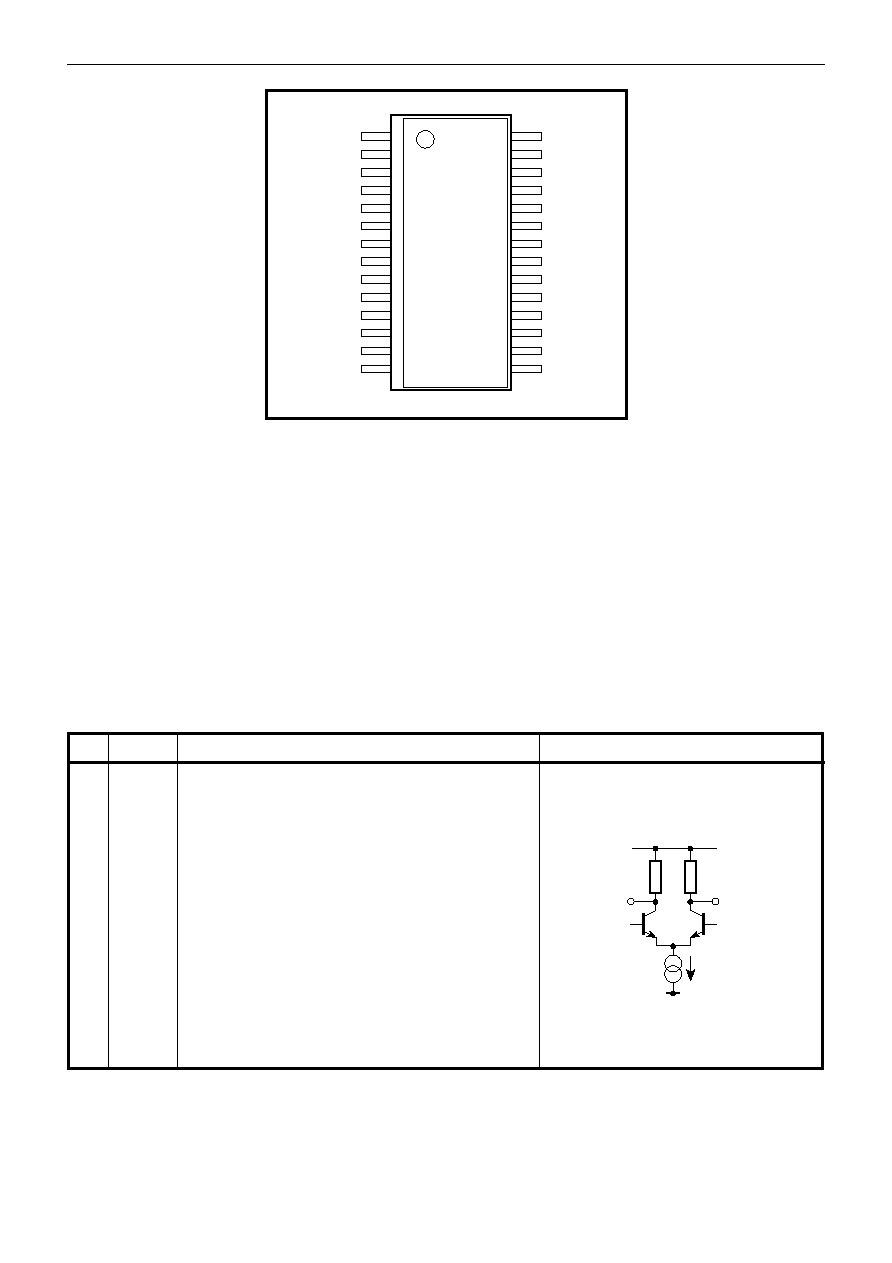
Figure 2 Pin connections (top view)
the performance for a wide range of applications and
locations world wide.
T
he KESRX05, with its anti-jamming detector circuit, is
an ideal ASK/ OOK receiver for difficult reception areas
caused by interference such as amateur radio repeater
stations and wireless stereo headphones. Operation is
possible with interfering signals which are more than
20dB stronger than the wanted signal (IF bandwidth =
470kHz.), without the cost penalities of increased IF se-
lectivity and frequency accuracy.
Figure 1 is the system block diagram, with an external
ceramic IF filter, SAW fillter and noise reduction filter.
IFFLT1
IFDC1
IFIN
IFDC2
V
CC
IFOUT
V
CC
RF
MIXIP
RFOP
V
EE
RF
RFIN
AGC
PEAK
DATAOP
IFFLT2
RSSI
DETB
PD
XTAL1
XTAL2
DF0
DF1
DF2
VCO1
VCO2
V
EE
LF
DSN
1
2
3
4
5
6
7
8
9
10
11
12
13
14
28
27
26
25
24
23
22
21
20
19
18
17
16
15
KESRX05
DESCRIPTION
The single conversion superheterodyne receiver
approach is now generally considered the way forward
for ISM band type applications because of lower cost,
superior selectivity, lower radiation, and flexibility over
other techniques. For power-conscious, hand-held
applications KESRX05 provides improved performance
and flexibility on a lower 3∑0V supply and a power down
feature allows faster switch-on times for use in a pulsed
power saving mode.
Although this is a relatively simple receiver, the flexibility
of using an external IF filter allows the designer to
choose both the selectivity and the IF in order to optimise
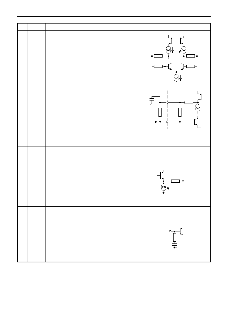
Pin
Name
Function
Schematic
1
IFFLT1
Table 1 Pin descriptions
Cont...
IFFLT1
IFFLT2
10k
10k
V
CC
Noise reducing IF filter
A simple LC noise reduction filter (L5 and C7) is
connected between pins 1 (IFFLT1 ) and 28 (IFFLT2)
to reduce the noise contribution from the earlier
stages of the logathrimic amplifier. The LC filter helps
to reduce the bandwidth of the log amplifier from
approximately 45MHz to typically 1MHz, preventing
wideband noise from being detected as a signal. To
reduce the Q of the simple LC circuit, an external
damping resistor in parallel with L5, C7. However,
the preferred method to a damping resistor is to lower
the Q of L5 or increase the tolerances of L5 and C7.
For further information refer to the
IF Amp /RSSI Detector section of the Functional Description.
3
KESRX05
Pin
Name
Function
Schematic
2
3
4
5
6
7
8
IFDC1
IFIN
IFDC2
V
CC
IFOUT
V
CC
RF
MIXIP
Log Amplifier DC Blocking Capacitor
Capacitors C3 and C4 provide DC blocking within
the high gain stage of the log amplifier. The log
amplifier has a small gain of greater than 80dB
between pins 3 (IFIN) and 27 (RSSI output)
Capacitors C3 and C4 eliminate DC offsets, allowing
the amplification of AC signals only.
For further information, refer to the IF Amp/RSSI De-
tector section of the Functional Description.
Log Amp Input (IFamplifier input)
The bandwidth of KESRX05 is set by the external
ceramic filter CF1. Impedance matching from the
output of the ceramic filter to the input of the log
amplifier is achieved by an external shunt resistor
R9 in parallel with an internal resistor.
For further information please refer to the IF Interface
section of the Functional Description.
Log amplifier DC stability capacitor
Positive supply
IF output
The IF output drive is a voltage drive with a low output
impedance of 300
via an internal series resistor.
The IFOUT pin is designed for direct connection to
an external 10∑7MHz FM ceramic filter with a typical
input impedance of 300
.
For further information refer to the IF Interface section
of the Functional Description.
Positive supply for RF circuits
Mixer input
To a first order approximation the input impedance
of the mixer at UHF frequencies is set by the internal
bias resistor and capacitor network. Effects of internal
and external stray parasitics ignored.
For further information refer to the AC Electrical
Characteristics.
IFIN
3∑1k
950
181k
181k
IFDC
IFDC1
IFDC1
IFIN
3∑1k
181k
INTERNAL
R9
FROM
CF1
C3
Matching circuit for CF1
See pin 2
Table 1 Pin descriptions (continued)
Cont...
IFOUT
300
50
µA
MIXIP
2k
2p
V
EE
RF
4
KESRX05
Pin
Name
Function
Schematic
9
10
11
12
13
14
RFOUT
V
EE
RF
RFIN
AGC
PEAK
DATAOP
Output from internal RF amplifier
The RF amplifier has a high output impedance. The
internal 300
resistor is used to improve the ESD
protection of RFOUT.
For further information refer to the AC Electrical
Characteristics.
Negative supply for RF circuits
nternal input RF amplifier
To a first order approximation the input impedance
of the RF amplifier at UHF frequencies is set by the
internal bias resistor and capacitor network. Effects
of internal and external stray parasitics ignored.
For further information please refer to the AC
Electrical Characteristics.
RF AGC time constant
The attack and decay time constant of the AGC is
set by the internal series resistor, current sink and
the external capacitor C8. Increasing the decay time
constant of the AGC circuit will impair the time to
good data of the receiver from power up PD0 to PD2.
For further information please refer to the IF Amp/
RSSI Detector section of the Functional Description.
Data signal peak detector output
The peak detector output is designed to be a low
impedance output. The peak detector monitors the
peak of the signal at pin 20 (DF2).
For further information please refer to the Baseband
section of the Functional Description.
Sliced data output
The data output is the inverted sense of the input
signal at pin 20 (DF2) and is designed as a high im-
pedance output via two internal sink and source cur-
rent generators
RFOP
300
240
µA
(AGC OFF)
830
10p
5p
1k
RFIN
V
EE
RF
240
µA
360
AGC
6
µA
190k
300
PEAK
V
EE
DATAOP
1
20
µA
2
20
µA
HIGH
LOW
Table 1 Pin descriptions (continued)
Cont...