 | –≠–ª–µ–∫—Ç—Ä–æ–Ω–Ω—ã–π –∫–æ–º–ø–æ–Ω–µ–Ω—Ç: L50402GDG | –°–∫–∞—á–∞—Ç—å:  PDF PDF  ZIP ZIP |
Document Outline
- Zarlink Features
- L2 Switching
- VLAN Support Features
- Classification and Security
- Traffic Management
- Network Management Support
- Description
- Changes Summary
- July 2003
- November 2003
- February 2004
- August 2004
- November 2004
- January 2005
- June 2005
- December 2005
- April 2006
- 1.0 BGA and Ball Signal Descriptions
- 1.1 BGA Views (Top-View)
- 1.2 Power and Ground Distribution
- 1.3 Ball Signal Descriptions
- 1.4 Signal Mapping and Internal pull-up/Down Configuration
- 1.5 Bootstrap Options
- 1.5.1 Recommended Default Bootstrap Settings
- 1.6 Default Switch Configuration and Initialization Sequence
- 1.7 Power Sequencing
- 2.0 Block Functionality
- 2.1 Internal Memory
- 2.2 MAC Modules
- 2.2.1 RMII MAC Module (RMAC)
- 2.2.1.1 GPSI (7WS) Interface
- 2.2.2 CPU MAC Module (CMAC)
- 2.2.3 GMII MAC Module (GMAC)
- 2.2.4 PHY Addresses
- 2.3 Management Module
- 2.4 Frame Engine
- 2.5 Search Engine
- 2.6 Timeout Reset Monitor
- 2.7 JTAG
- 2.7.1 Registers
- 2.7.2 Test Access Port (TAP) Controller
- 2.7.3 Boundary Scan Instructions
- 3.0 Management and Configuration
- 3.1 Register Configuration, Frame Transmission and Frame Reception
- 3.1.1 Register Configuration
- 3.1.2 Rx/Tx of Standard Ethernet Frames
- 3.1.3 Control Frames
- 3.2 I2C Interface
- 3.2.1 Start Condition
- 3.2.2 Address
- 3.2.3 Data Direction
- 3.2.4 Acknowledgment
- 3.2.5 Data
- 3.2.6 Stop Condition
- 3.3 Synchronous Serial Interface
- 3.3.1 Write Command
- 3.3.2 Read Command
- 4.0 Data Forwarding Protocol
- 4.1 Unicast Data Frame Forwarding
- 4.2 Multicast Data Frame Forwarding
- 4.3 Frame Forwarding To and From CPU
- 5.0 Search Engine
- 5.1 Search Engine Overview
- 5.2 Basic Flow
- 5.3 Search, Learning and Aging
- 5.3.1 MAC Search
- 5.3.2 Learning
- 5.3.3 Aging
- 5.4 MAC Address Filtering
- 5.5 Protocol Filtering
- 5.6 Logical Port Filtering
- 5.7 Quality of Service
- 5.8 Priority Classification Rule
- 5.9 Port and Tag Based VLAN
- 5.9.1 Port-Based VLAN
- 5.9.2 Tag-Based VLAN
- 5.9.3 VLAN Stacking (Q-in-Q)
- 5.10 IP Multicast Switching
- 5.11 L2 Multicast Switching
- 6.0 Frame Engine
- 6.1 Data Forwarding Summary
- 6.2 Frame Engine Details
- 6.2.1 FCB Manager
- 6.2.2 Rx Interface
- 6.2.3 RxDMA
- 6.2.4 TxQ Manager
- 6.2.5 Port Control
- 6.2.6 TxDMA
- 7.0 Quality of Service and Flow Control
- 7.1 Model
- 7.2 Two QoS Configurations
- 7.2.1 Strict Priority
- 7.2.2 Weighted Fair Queuing
- 7.3 WRED Drop Threshold Management Support
- 7.4 Shaper
- 7.5 Rate Control
- 7.6 Buffer Management
- 7.6.1 Dropping When Buffers Are Scarce
- 7.7 Flow Control Basics
- 7.7.1 Unicast Flow Control
- 7.7.2 Multicast Flow Control
- 7.8 Mapping to IETF Diffserv Classes
- 8.0 Traffic Mirroring
- 8.1 Mirroring Features
- 8.2 Using port mirroring for loop back
- 9.0 Clocks
- 9.1 Clock Requirements
- 9.1.1 System Clock (SCLK) Speed Requirement
- 9.1.2 RMAC Reference Clock (M_CLK) Speed Requirement
- 9.1.3 GMAC Reference Clock (GREF_CLK) Speed Requirement
- 9.1.4 JTAG Test Clock (TCK) Speed Requirements
- 9.2 Clock Generation
- 9.2.1 MDC
- 9.2.2 SCL
- 9.2.3 Ethernet Interface Clocks
- 10.0 Hardware Statistics Counters
- 10.1 Hardware Statistics Counters List
- 10.2 IEEE 802.3 HUB Management (RFC 1516)
- 10.2.1 Event Counters
- 10.2.1.1 PortReadableFrames
- 10.2.1.2 PortReadableOctets
- 10.2.1.3 PortFCSErrors
- 10.2.1.4 PortAlignmentErrors
- 10.2.1.5 PortFrameTooLongs
- 10.2.1.6 PortShortEvents
- 10.2.1.7 PortRunts
- 10.2.1.8 PortCollisions
- 10.2.1.9 PortLateEvents
- 10.2.1.10 PortVeryLongEvents
- 10.2.1.11 PortDataRateMisatches
- 10.2.1.12 PortAutoPartitions
- 10.2.1.13 PortTotalErrors
- 10.3 IEEE 802.1 Bridge Management (RFC 1286)
- 10.3.1 Event Counters
- 10.3.1.1 PortDelayExceededDiscards
- 10.3.1.2 PortMtuExceededDiscards
- 10.3.1.3 PortInFrames
- 10.3.1.4 PortOutFrames
- 10.3.1.5 PortInDiscards
- 10.4 RMON - Ethernet Statistic Group (RFC 1757)
- 10.4.1 Event Counters
- 10.4.1.1 DropEvents
- 10.4.1.2 Octets
- 10.4.1.3 Pkts
- 10.4.1.4 BroadcastPkts
- 10.4.1.5 MulticastPkts
- 10.4.1.6 CRCAlignErrors
- 10.4.1.7 UndersizePkts
- 10.4.1.8 OversizePkts
- 10.4.1.9 Fragments
- 10.4.1.10 Jabbers
- 10.4.1.11 Collisions
- 10.4.1.12 Packet Count for Different Size Groups
- 10.5 Miscellaneous Counters
- 11.0 Register Definition
- 11.1 ZL50402 Register Description
- 11.2 Directly Accessed Registers
- 11.3 Indirectly Accessed Registers
- 11.3.1 (Group 0 Address) MAC Ports Group
- 11.3.1.1 ECR1Pn: Port n Control Register
- 11.3.1.2 ECR2Pn: Port n Control Register
- 11.3.1.3 ECR3Pn: Port n Control Register
- 11.3.1.4 ECR4Pn: Port n Control Register
- 11.3.1.5 BUF_LIMIT - Frame Buffer Limit
- 11.3.1.6 FCC - Flow Control Grant Period
- 11.3.2 (Group 1 Address) VLAN Group
- 11.3.2.1 AVTCL - VLAN Type Code Register Low
- 11.3.2.2 AVTCH - VLAN Type Code Register High
- 11.3.2.3 PVMAP00_0 - Port 0 Configuration Register 0
- 11.3.2.4 PVMAP00_1 - Port 0 Configuration Register 1
- 11.3.2.5 PVMAP00_3 - Port 0 Configuration Register 3
- 11.3.2.6 PVMAPnn_0,1,3 - Ports 1~9 Configuration Registers
- 11.3.2.7 PVMODE
- 11.3.3 (Group 3 Address) CPU Port Configuration Group
- 11.3.3.1 MAC0 - CPU MAC address byte 0
- 11.3.3.2 MAC1 - CPU MAC address byte 1
- 11.3.3.3 MAC2 - CPU MAC address byte 2
- 11.3.3.4 MAC3 - CPU MAC address byte 3
- 11.3.3.5 MAC4 - CPU MAC address byte 4
- 11.3.3.6 MAC5 - CPU MAC address byte 5
- 11.3.3.7 INT_MASK0 - Interrupt Mask
- 11.3.3.8 INTP_MASK0 - Interrupt Mask for MAC Port 0,1
- 11.3.3.9 INTP_MASKn - Interrupt Mask for MAC Ports 8~9 Registers
- 11.3.3.10 RQS - Receive Queue Select
- 11.3.3.11 RQSS - Receive Queue Status
- 11.3.3.12 MAC01 - Increment MAC port 0,1 address
- 11.3.3.13 MAC9 - Increment MAC port 9 address
- 11.3.3.14 CPUQINS0 - CPUQINS6 - CPU Queue Insertion Command
- 11.3.3.15 CPUQINSRPT - CPU Queue Insertion Report
- 11.3.3.16 CPUGRNHDL0 - CPUGRNHDL1 - CPU Allocated Granule Pointer
- 11.3.3.17 CPURLSINFO0 - CPURLSINFO4 - Receive Queue Status
- 11.3.3.18 CPUGRNCTR - CPU Granule Control
- 11.3.4 (Group 4 Address) Search Engine Group
- 11.3.4.1 AGETIME_LOW - MAC address aging time Low
- 11.3.4.2 AGETIME_HIGH -MAC address aging time High
- 11.3.4.3 SE_OPMODE - Search Engine Operation Mode
- 11.3.5 (Group 5 Address) Buffer Control/QOS Group
- 11.3.5.1 QOSC - QOS Control
- 11.3.5.2 PCC - Packet Congestion Control
- 11.3.5.3 MCC - Multicast Congestion Control
- 11.3.5.4 MCCTH - Multicast Threshold Control
- 11.3.5.5 RDRC0 - WRED Rate Control 0
- 11.3.5.6 RDRC1 - WRED Rate Control 1
- 11.3.5.7 RDRC2 - WRED Rate Control 2
- 11.3.5.8 SFCB - Share FCB Size
- 11.3.5.9 C1RS - Class 1 Reserve Size
- 11.3.5.10 C2RS - Class 2 Reserve Size
- 11.3.5.11 C3RS - Class 3 Reserve Size
- 11.3.5.12 AVPML - VLAN Tag Priority Map
- 11.3.5.13 AVPMM - VLAN Priority Map
- 11.3.5.14 AVPMH - VLAN Priority Map
- 11.3.5.15 AVDM - VLAN Discard Map
- 11.3.5.16 TOSPML - TOS Priority Map
- 11.3.5.17 TOSPMM - TOS Priority Map
- 11.3.5.18 TOSPMH - TOS Priority Map
- 11.3.5.19 TOSDML - TOS Discard Map
- 11.3.5.20 USER_PROTOCOL_n - User Define Protocol 0~7
- 11.3.5.21 USER_PROTOCOL_FORCE_DISCARD - User Define Protocol 0~7 Force Discard
- 11.3.5.22 WELL_KNOWN_PORT[1:0]_PRIORITY- Well Known Logic Port 1 and 0 Priority
- 11.3.5.23 WELL_KNOWN_PORT[3:2]_PRIORITY- Well Known Logic Port 3 and 2 Priority
- 11.3.5.24 WELL_KNOWN_PORT[5:4]_PRIORITY- Well Known Logic Port 5 and 4 Priority
- 11.3.5.25 WELL_KNOWN_PORT[7:6]_PRIORITY- Well Known Logic Port 7 and 6 Priority
- 11.3.5.26 WELL_KNOWN_PORT_ENABLE - Well Known Logic Port 0 to 7 Enables
- 11.3.5.27 WELL_KNOWN_PORT_FORCE_DISCARD - Well Known Logic Port 0~7 Force Discard
- 11.3.5.28 USER_PORT[7:0]_[LOW/HIGH] - User Define Logical Port 0~7
- 11.3.5.29 USER_PORT_[1:0]_PRIORITY - User Define Logic Port 1 and 0 Priority
- 11.3.5.30 USER_PORT_[3:2]_PRIORITY - User Define Logic Port 3 and 2 Priority
- 11.3.5.31 USER_PORT_[5:4]_PRIORITY - User Define Logic Port 5 and 4 Priority
- 11.3.5.32 USER_PORT_[7:6]_PRIORITY - User Define Logic Port 7 and 6 Priority
- 11.3.5.33 USER_PORT_ENABLE[7:0] - User Define Logic Port 0 to 7 Enables
- 11.3.5.34 USER_PORT_FORCE_DISCARD[7:0] - User Define Logic Port 0~7 Force Discard
- 11.3.5.35 RLOWL - User Define Range Low Bit 7:0
- 11.3.5.36 RLOWH - User Define Range Low Bit 15:8
- 11.3.5.37 RHIGHL - User Define Range High Bit 7:0
- 11.3.5.38 RHIGHH - User Define Range High Bit 15:8
- 11.3.5.39 RPRIORITY - User Define Range Priority
- 11.3.6 (Group 6 Address) MISC Group
- 11.3.6.1 MII_OP0 - MII Register Option 0
- 11.3.6.2 MII_OP1 - MII Register Option 1
- 11.3.6.3 FEN - Feature Enable Register
- 11.3.6.4 MIIC0 - MII Command Register 0
- 11.3.6.5 MIIC1 - MII Command Register 1
- 11.3.6.6 MIIC2 - MII Command Register 2
- 11.3.6.7 MIIC3 - MII Command Register 3
- 11.3.6.8 MIID0 - MII Data Register 0
- 11.3.6.9 MIID1 - MII Data Register 1
- 11.3.6.10 USD - One Micro Second Divider
- 11.3.6.11 DEVICE - Device Mode
- 11.3.6.12 CHECKSUM - EEPROM Checksum
- 11.3.6.13 fMACCReg0, fMACCReg1 - MAC Control Frame OpCode
- 11.3.6.14 FCB Base Address Register 0
- 11.3.6.15 FCB Base Address Register 1
- 11.3.6.16 FCB Base Address Register 2
- 11.3.7 (Group 7 Address) Port Mirroring Group
- 11.3.7.1 MIRROR CONTROL - Port Mirror Control Register
- 11.3.7.2 MIRROR_DEST_MAC[5:0] - Mirror Destination MAC Address 0~5
- 11.3.7.3 MIRROR_SRC _MAC[5:0] - Mirror Source MAC Address 0~5
- 11.3.7.4 RMII_MIRROR0 - RMII Mirror 0
- 11.3.7.5 RMII_MIRROR1 - RMII Mirror 1
- 11.3.8 (Group 8 Address) Per Port QOS Control
- 11.3.8.1 FCRn - Port 0~1,8,9 Flooding Control Register
- 11.3.8.2 BMRCn - Port 0~1,8,9 Broadcast/Multicast Rate Control
- 11.3.8.3 PR100_n - Port 0~1 Reservation
- 11.3.8.4 PR100_CPU - Port CPU Reservation
- 11.3.8.5 PRG - Port GMAC Reservation
- 11.3.8.6 PTH100_n - Port 0~1 Threshold
- 11.3.8.7 PTH100_CPU - Port CPU Threshold
- 11.3.8.8 PTHG - Port GMAC Threshold
- 11.3.8.9 QOSC00, QOSC01 - Classes Byte Limit port 0
- 11.3.8.10 QOSC02, QOSC03 - Classes Byte Limit port 1
- 11.3.8.11 QOSC16 - QOSC21 - Classes Byte Limit CPU port
- 11.3.8.12 QOSC22 - QOSC27 - Classes Byte Limit GMAC port
- 11.3.8.13 QOSC28 - QOSC31 - Classes WFQ Credit For GMAC
- 11.3.8.14 QOSC36 - QOSC39 - Shaper Control Port GMAC
- 11.3.9 (Group E Address) System Diagnostic
- 11.3.9.1 DTSRL - Test Output Selection
- 11.3.9.2 DTSRM - Test Output Selection
- 11.3.9.3 TESTOUT0, TESTOUT1 - Testmux Output [7:0], [15:8]
- 11.3.9.4 MASK0-MASK4 - Timeout Reset Mask
- 11.3.9.5 BOOTSTRAP0 - BOOTSTRAP3
- 11.3.9.6 PRTFSMST0~1,8,9
- 11.3.9.7 PRTQOSST0-PRTQOSST1
- 11.3.9.8 PRTQOSST8A, PRTQOSST8B (CPU port)
- 11.3.9.9 PRTQOSST9A, PRTQOSST9B (GMAC port)
- 11.3.9.10 CLASSQOSST
- 11.3.9.11 PRTINTCTR
- 11.3.9.12 QMCTRL0~1,8,9
- 11.3.9.13 QCTRL
- 11.3.9.14 BMBISTR0, BMBISTR1
- 11.3.9.15 BMControl
- 11.3.9.16 BUFF_RST
- 11.3.9.17 FCB_HEAD_PTR0, FCB_HEAD_PTR1
- 11.3.9.18 FCB_TAIL_PTR0, FCB_TAIL_PTR1
- 11.3.9.19 FCB_NUM0, FCB_NUM1
- 11.3.9.20 BM_RLSFF_CTRL
- 11.3.9.21 BM_RSLFF_INFO[5:0]
- 11.3.10 (Group F Address) CPU Access Group
- 11.3.10.1 GCR - Global Control Register
- 11.3.10.2 DCR - Device Status and Signature Register
- 11.3.10.3 DCR1 - Device Status Register 1
- 11.3.10.4 DPST - Device Port Status Register
- 11.3.10.5 DTST - Data read back register
- 11.3.10.6 DA - Dead or Alive Register
- 12.0 Characteristics and Timing
- 12.1 Absolute Maximum Ratings
- 12.2 DC Electrical Characteristics
- 12.3 Recommended Operating Conditions
- 12.4 AC Characteristics and Timing
- 12.4.1 Typical Reset & Bootstrap Timing Diagram
- 12.4.2 Typical CPU Timing Diagram for a CPU Write Cycle
- 12.4.3 Typical CPU Timing Diagram for a CPU Read Cycle
- 12.4.4 Synchronous Serial Interface (SSI)
- 12.4.5 EEPROM Inter-Integrated Circuit (I∑C)
- 12.4.6 Reduced Media Independent Interface (RMII)
- 12.4.7 Media Independent Interface (MII)
- 12.4.8 Reverse Media Independent Interface (RvMII)
- 12.4.9 General Purpose Serial Interface (GPSI)
- 12.4.10 Reverse General Purpose Serial Interface (RvGPSI)
- 12.4.11 Gigabit Media Independent Interface (GMII)
- 12.4.12 MII Management Data Interface (MDIO/MDC)
- 12.4.13 JTAG (IEEE 1149.1-2001)
1
Zarlink Semiconductor Inc.
Zarlink, ZL and the Zarlink Semiconductor logo are trademarks of Zarlink Semiconductor Inc.
Copyright 2003-2006, Zarlink Semiconductor Inc. All Rights Reserved.
Zarlink Features
∑ Integrated Single-Chip 10/100/1000 Mbps
Ethernet Switch
∑ Two 10/100 Mbps auto-negotiating Fast
Ethernet (FE) ports with RMII, MII, GPSI,
Reverse MII & Reverse GPSI interface options
∑ One 10/100/1000 Mbps auto-negotiating port
with GMII & MII interface options, that can be
used as a WAN uplink or as a 9th port
∑ a 10/100 Mbps Fast Ethernet (FE) CPU port
with Reverse MII interface option
∑ Embedded 2.0 Mbits (256 KBytes) internal
memory for control databases and frame data
buffer
∑ Supports jumbo frames up to 4 KBytes
∑ CPU access supports the following interface
options:
∑ 8/16-bit ISA interface
∑ Serial interface with MII port; recommended
for light management
∑ Serial interface in lightly managed mode, or in
unmanaged mode with optional I
2
C EEPROM
interface
∑ Ethernet IEEE 802.3x flow control for full duplex
ports, back pressure flow control for half duplex
ports
∑ Built-in reset logic triggered by system
malfunction
∑ Built-In Self Test for internal SRAM
∑ IEEE-1149.1 (JTAG) test port
L2 Switching
∑ L2 switching
∑ MAC address self learning, up to 4 K MAC
addresses
∑ MAC address table supports unicast and
multicast MAC address and IP multicast
address learning
∑ Supports IP Multicast with IGMP snooping, up to
4 K IP Multicast groups
April 2006
Ordering Information
ZL50402GDG
208-Ball LBGA
ZL50402GDG2
208-Ball LBGA**
**Pb Free Tin/Silver/Copper
-40
∞
C to +85
∞
C
ZL50402
Managed 2FE + 1GE Layer-2
Ethernet Switch
Data Sheet
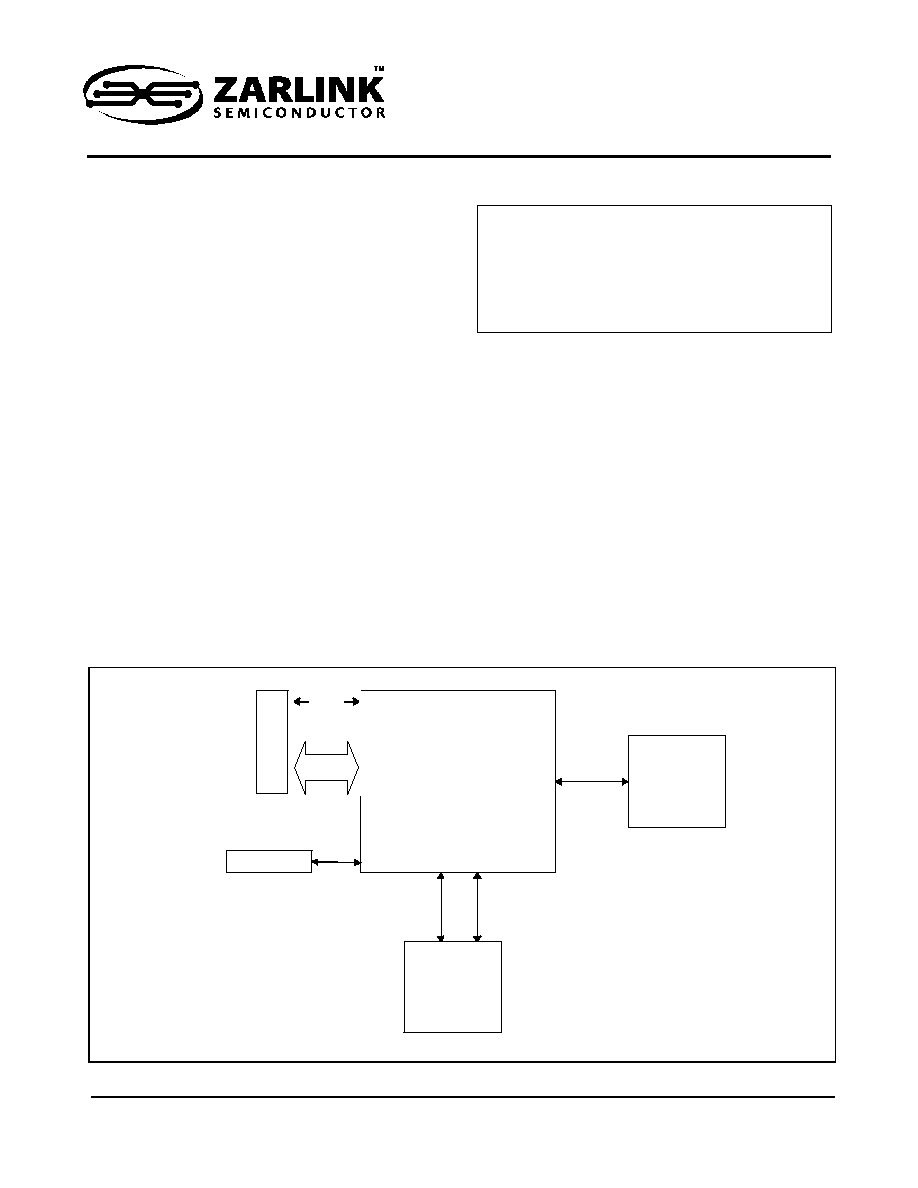
Figure 1 - System Block Diagram
2-Port 10/100M + 1G
Ethernet Switch
10/100/
1000
PHY
C
P
U
EEPROM
I
2
C
GM II / M II
Dual
10/100
PHY
RM II / M II / GPSI
8/16-bit
or
Serial
MII
ZL50402

ZL50402
Data Sheet
2
Zarlink Semiconductor Inc.
∑ Supports the following spanning standards
∑ IEEE 802.1D spanning tree
∑ IEEE 802.1w rapid spanning tree
∑ Supports Ethernet multicasting and broadcasting and flooding control
VLAN Support Features
∑ Supports the following VLAN standards
∑ port-based VLAN
∑ IEEE 802.1Q tag-based VLAN, up to 4 K VLANs
∑ Supports both shared VLAN learning (SVL) and independent VLAN learning (IVL) of MAC addresses
∑ Limited support for VLAN stacking ("Q-in-Q")
Classification and Security
∑ Search engine classification
∑ Classifies packets based on single field
- Source and destination L4 logical ports, or
- TOS/DS, or
- VLAN (IEEE 802.1p), or
- Physical port
∑ Assigns a transmission priority and drop precedence
∑ Packet filtering and security
∑ Static address filtering for source and/or destination MAC addresses
∑ Static MAC address not subject to aging
∑ Secure mode freezes MAC address learning (each port may independently use this mode)
∑ IEEE 802.1x access control
∑ Port-based priority: VLAN priority in a tagged frame can be overwritten by the priority of port VLAN ID
Traffic Management
∑ Two (2) transmission classes for FE ports and four (4) transmission classes for uplink port
∑ Scheduling using weighted fair queuing (WFQ) or strict priority (SP) discipline
∑ At egress, per-queue weighted random early discard (WRED) with 2 drop precedence levels
∑ Configurable WRED thresholds
∑ For FE ports, supports ingress and egress rate control
∑ Bandwidth rationing, Bandwidth on demand, SLA (Service Level Agreement)
∑ Granularity of rate regulation to 16 Kbps
∑ Ingress rate regulated using WRED, with 2 drop precedence levels, or flow control
∑ Output traffic regulation per class available on uplink port
∑ Fully supports Differentiated Services' Expedited and Assured Forwarding (EF and AF) per-hop behaviours
∑ Intelligent buffer management
∑ Achieves high buffer utilization while ensuring fairness among traffic classes and ports
∑ Buffer reservations per class and per source port
∑ Supports concentration mode
∑ Traffic Mirroring
∑ Physical port based (RMII enabled ports only)
∑ Source or destination MAC address based
∑ MAC address pair based
∑ Supports module hot swap on all ports

ZL50402
Data Sheet
3
Zarlink Semiconductor Inc.
Network Management Support
∑ Built-in RMON MIB counters
Description
The ZL50402 is a low density, low cost, high performance, non-blocking Ethernet switch chip. A single chip
provides 2 ports at 10/100 Mbps, 1 uplink port at 10/100/1000 Mbps, and a CPU interface for managed, lightly
managed and unmanaged switch applications. The chip supports up to 4 K MAC addresses and up to 4 K
tagged-based Virtual LANs (VLANs).
With strict priority and/or WFQ transmission scheduling and WRED dropping schemes, the ZL50402 provides
powerful QoS functions for various multimedia and mission-critical applications. The chip provides 2 transmission
priorities (4 priorities for uplink port) and 2 levels of dropping precedence. Each packet is assigned a transmission
priority and dropping precedence based on the VLAN priority field in a VLAN tagged frame, or the DS/TOS field, or
the UDP/TCP logical port fields in IP packets. The ZL50402 recognizes a total of 16 UDP/TCP logical ports, 8
hard-wired and 8 programmable (including one programmable range).
In half-duplex mode, all ports support backpressure flow control, to minimize the risk of losing data during long
activity bursts. In full-duplex mode, IEEE 802.3x flow control is provided. The ZL50402 also supports a per-system
option to enable flow control for best effort frames, even on QoS-enabled ports.
Statistical information for SNMP and the Remote Monitoring Management Information Base (RMON MIB) are
collected independently for all ports. Access to these statistical counters/registers is provided via the CPU interface.
SNMP Management frames can be received and transmitted via the CPU interface, creating a complete network
management solution.
The ZL50402 is fabricated using 0.18 micron technology. The ZL50402 is packaged in a 208-pin Ball Grid Array
package.

ZL50402
Data Sheet
4
Zarlink Semiconductor Inc.
Changes Summary
July 2003
∑ Initial Release
November 2003
∑ Clarified IP Multicast support is up to 4K groups, as it wasn't mentioned in the data sheets
∑ Updated Ball Signal Description Table (1.3, "Ball Signal Descriptions" on page 14):
∑ clarified the ball signal I/O description for Mn_TXCLK & Mn_RXCLK showing these signals are either
inputs OR outputs
∑ clarified that M9_MTXCLK is an input only
∑ Updated 1.4, "Signal Mapping and Internal pull-up/Down Configuration" on page 20 to indicate operation of
the internal pull-up/down resistors in different modes
∑ Clarified 9.1.3, "GMAC Reference Clock (GREF_CLK) Speed Requirement" on page 52 on usage of
GREF_CLK
∑ Clarified PVMODE register bit description for bits [2] & [5]
∑ Updated ECR4Pn register description as port 9 (uplink) operates differently than the RMAC ports for MII
bi-directional clocking (bits [1:0])
∑ I
2
C address mapping was corrected for QOSCn registers
∑ Added Maximum Junction Temperature to 12.1, "Absolute Maximum Ratings" on page 122
∑ Updated I/O voltage levels to use TTL spec values rather than % of Vcc (12.2, "DC Electrical
Characteristics" on page 122)
February 2004
∑ Added the following to the Feature List:
∑ 4 K jumbo frames
∑ IEEE 802.3ad support
∑ Reverse MII/GPSI
∑ Added section on PHY addresses (2.2.4, "PHY Addresses" on page 28)
∑ Clarified that they are hard-coded
∑ Fixed error in DS on sending Ethernet Frames via 8/16-bit or serial interface.
∑ The Status Bytes is sent before the frame, for both Tx and Rx
∑ Added more cross-references to available AppNotes
∑ Added section on Stacked VLAN (Q-in-Q) (5.9.3, "VLAN Stacking (Q-in-Q)" on page 43) and IP Multicast
Switching (5.10, "IP Multicast Switching" on page 44) since they weren't really discussed in the DS
∑ Added more clock descriptions to 9.0, "Clocks" on page 52
∑ INT_MASK and INTP_MASK registers should state that the default register value is 0x00
August 2004
∑ Added section Changes Summary to document
∑ Added section on SCL clock generation (9.2.2, "SCL" on page 52)
∑ Interrupt Register was incorrectly identified as read only, should be read/write
∑ Clarified that only bit [7] is not self-clearing
∑ Updated CPU timing diagrams to clarify timing (12.4, "AC Characteristics and Timing" on page 124)
November 2004
∑ Added section 1.6, "Default Switch Configuration and Initialization Sequence" on page 24
∑ Updated CPU timing diagrams to clarify P_A timing (12.4, "AC Characteristics and Timing" on page 124)

ZL50402
Data Sheet
5
Zarlink Semiconductor Inc.
January 2005
∑ Updated GMII timing (12.4.11, "Gigabit Media Independent Interface (GMII)" on page 134)
∑ reduce min. hold time from 1ns to 0.5ns
∑ reduced max. output delay by 1ns
∑ Removed reference to direct register INDEX_REG1 (address 0x1) from SSI diagrams, as not applicable
June 2005
∑ Added 2FE+1GE variant
∑ Corrected ordering code to ZL50402GD"G"
∑ Clarified that port mirroring is only available if the source & destination ports are in RMII mode
∑ Updated PVMODE bit [5] to reflect the proper MAC address range: 01-80-C2-00-00-00~F
∑ Clarified DATAOUT output can be open-drain or totem-pole based on debounce selection via bootstrap
TSTOUT[0]
∑ Added power sequencing recommendation (1.7, "Power Sequencing" on page 25)
∑ Added Reverse MII/GPSI timing characteristics (12.4.10, "Reverse General Purpose Serial Interface
(RvGPSI)" on page 133 and 12.4.12, "MII Management Data Interface (MDIO/MDC)" on page 136)
∑ Clarified that counter "DelayExceededDiscards" is not applicable for the ZL50402 (10.0, "Hardware Statistics
Counters" on page 53)
December 2005
∑ Clarified that TRST signal should be externally tied to GND via weak resistor, as per JTAG standard (1.3,
"Ball Signal Descriptions" on page 14)
∑ Added more text to section 2.7, "JTAG" on page 28
∑ Clarified counter definitions (10.0, "Hardware Statistics Counters" on page 53)
∑ Added more explaination to VLAN ID Hashing feature: register FEN, bit [3]
∑ Removed definition for SE_OPMODE bit[5] (ARP report control), as this feature was not implemented and
this bit was mistakenly left in the register definition.
April 2006
∑ Added Pb-free order code (ZL50402GDG2)
∑ Added section on multicast MAC address learning/switching (5.11, "L2 Multicast Switching" on page 44)
since it wasn't really discussed in the DS
∑ Clarified registers UCC, MCC & MCCTH
∑ Renamed register UCC (now PCC), as name was misleading
∑ Updated timing to CPU RvMII, as min. output delay should have been 0ns