
Obsolescence Notice
This product is obsolete.
This information is available for your
convenience only.
For more information on
Zarlink's obsolete products and
replacement product lists, please visit
http://products.zarlink.com/obsolete_products/

MA2901
1
The MA2901 is an industry standard 4-bit microprocessor
slice It provides a set of ALU functions selected by microcode
data applied to the inputs. The device is cascadable to handle
any word length. It can be used as a building block in the
construction of microcomputers and controllers tailored to
meet specialised applications.
Dual Address Architecture
Machine cycles are saved by simultaneous, independent
access to two working registers.
ALU has Eight Functions
Operations performed are addition, two subtractions and five
logic functions on two source operands.
Four State Flags
Zero, negative, carry and overflow.
Left / Right Shift is Independent of ALU
Only one cycle taken for add and shift operations.
Expandable
Any number of MA2901 units can be connected together to
achieve longer word lengths.
Micro Programmable
Three groups, each of three bits, for ALU function, source
operand and destination control.
DS3576-3.3
MA2901
RADIATION HARD 4-BIT MICROPROCESSOR SLICE
OPERATION
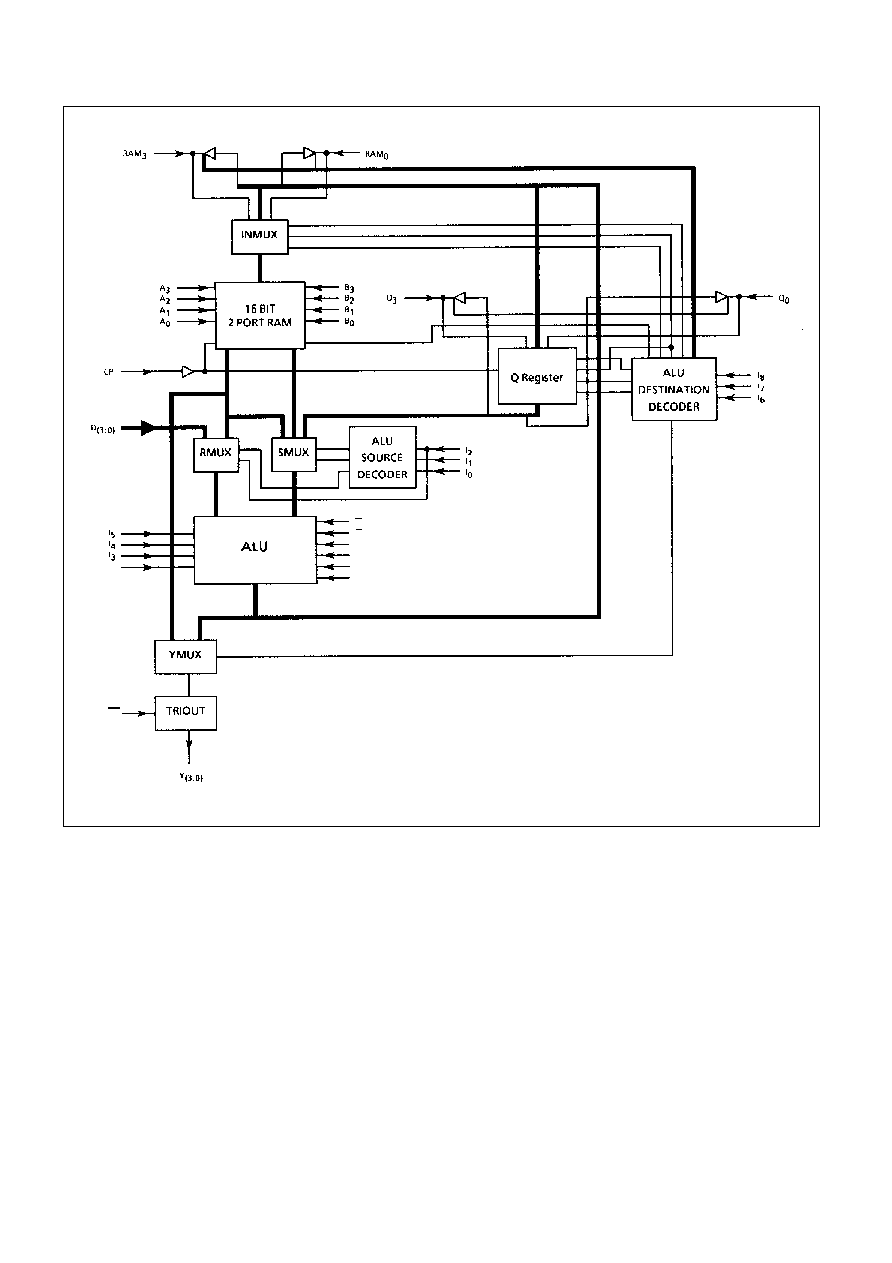
A detailed block diagram of the microprogrammable
microprocessor structure is shown in figure 1. The circuit is a
four-bit slice, cascadable to any number of bits. Therefore, all
data paths within the circuit are four bits wide. The two key
elements in the figure 1 are the 16-word by 4-bit 2-port RAM
and the high speed ALU.
Data from any of the 16 words of the Random Access
Memory (RAM) can be read from the A-port of the RAM as
controlled by the 4-bit A-address field input. Likewise, data
from any of the 16 words of the RAM as defined by the B-
address field input can be simultaneously read from the B-port
of the RAM. The same code can be applied to the A-select field
and B-select field in which case the identical file data will
appear at both the RAM A-port and B-port outputs
simultaneously.
When enabled by the RAM write enable (RAM EN), new
data is always written into the file (word) defined by the B-
address field of the RAM. The RAM data input field is driven by
a 3-input multiplexer. This configuration is used to shift the
ALU output data (F) if desired. This three-input multiplexer
scheme allows the data to be shifted up one bit position,
shifted down one bit position, or not shifted in either direction.
The RAM A-port data outputs and RAM B-port data outputs
drive separate 4-bit latches. These latches hold the RAM data
while the clock input is LOW. This eliminates any possible race
conditions that could occur while new data is being written into
the RAM.
The high-speed Arithmetic Logic Unit (ALU) can perform
three binary arithmetic and five logic operations on the two 4-
bit input words R and S. The R input field is driven from a 2-
input multiplexer, while S input field is driven from a 3-input
multiplexer. Both multiplexers also have an inhibit capability;
that is, no data is passed. This is equivalent to a "zero" source
operand.
The ALU R-input multiplexer has the RAM A-port and the
direct data inputs (D) connected as inputs. Likewise, the ALU
S-input multiplexer has the RAM A-port, the RAM B-port and
the Q register connected as inputs.
FEATURES
s
Fully Compatible with Industry Standard 2901
s
CMOS SOS Technology
s
High SEU Immunity and Latch-up Free
s
High Speed
s
Low Power
FEBRUARY 1995
MA2901
2
Figure 1: Block Diagram
C
n
OE
G
P
C
n+4
OVR
F=0
F
3
MA2901
3
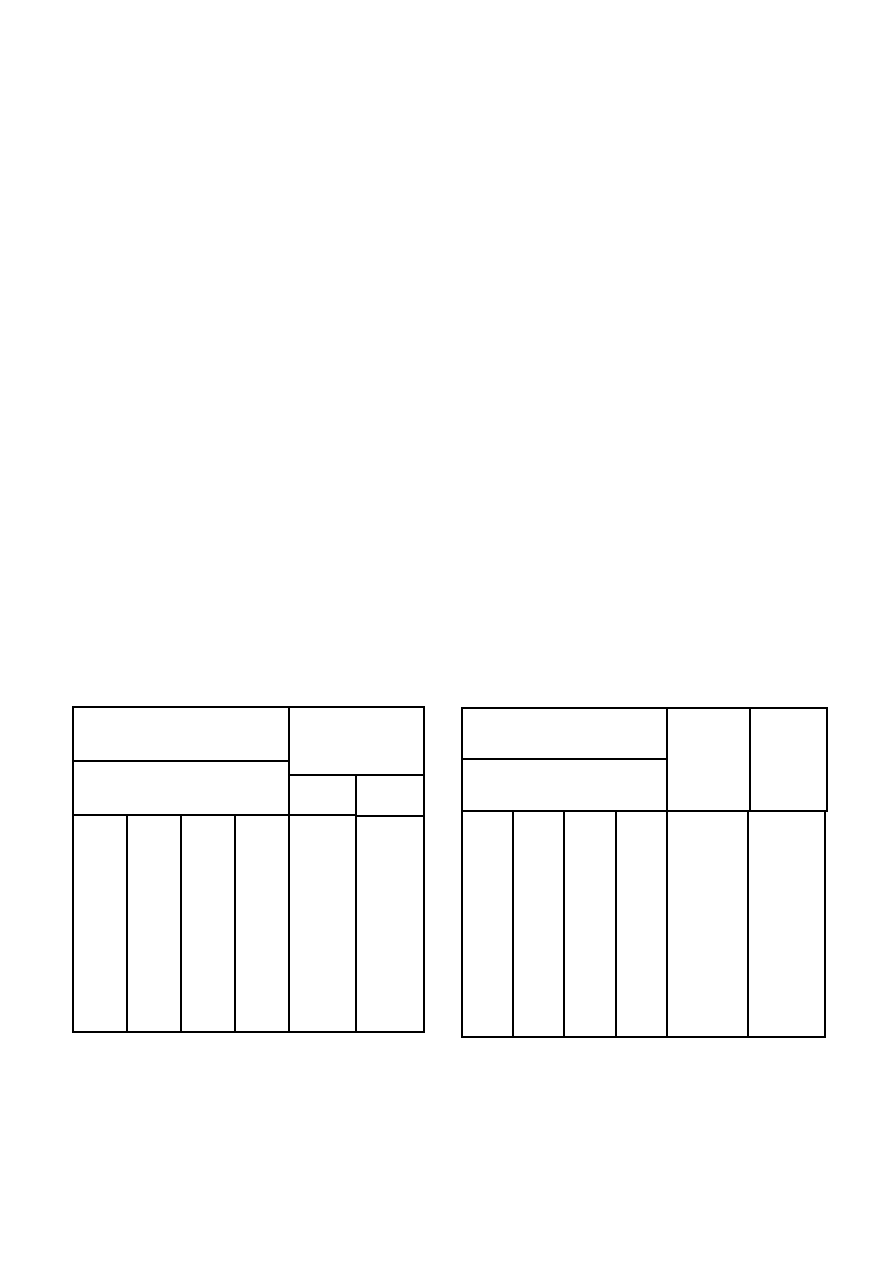
This multiplexer scheme gives the capability of selecting
various pairs of the A, B, D, Q and "0" inputs as source
operands to the ALU. These five inputs, when taken two at a
time, result in ten possible combinations of source operand
pairs. These combinations include AB, AD, AQ, A0, BD, BQ,
B0, DQ, D0 and Q0. It is apparent the AD, AQ and A0 are
somewhat redundant with BD, BQ and B0 in that if the A
address and B address are the same, the identical function
results. Thus, there are only seven completely non-redundant
sourced operand pairs for the ALU. The MA2901
microprocessor implements eight of these pairs. The
microinstruction inputs used to select the ALU source
operands are the l
0
, I
1
, and I
2
inputs. The definition of l
0
, I
1
, and
I
2
for the eight source operand combinations are as shown in
figure 2. Also shown is the octal code for each selection.
The two source operands not fully described as yet are the
D input and Q input. The D input is the four-bit wide direct data
field input. This port is used to insert all data into the working
registers inside the device. Likewise this input can be used in
the ALU to modify any of the internal data files. The Q register
is a separate 4-bit file intended primarily for multiplication and
division routines but it can also be used as an accumulator or
holding register for some applications.
The ALU itself is a high speed arithmetic/logic operator
capable of performing three binary arithmetic and five logic
functions. The I
3
, I
4
, and I
5
microinstruction inputs are used to
select the ALU function. The definition of these inputs is shown
in Figure 3. The octal code is also shown for reference. The
normal technique for cascading ALU of several devices is in a
look-ahead carry mode. Carry generate, GN, and carry
propagate, PN, are outputs of the device for use with a carry-
look-ahead-generator. A carry-out Cn + 4, is also generated
and is available as an output for use as the carry flag in a
status register. Both carry-in (Cn) and carry-out (Cn+4) are
active HIGH.
The ALU has three other status-oriented outputs. These
are F
3
, F=0, and overflow (OVR). The F
3
output is the most
significant (sign) bit of the ALU and can be used to determine
positive or negative results without enabling the three-state
data outputs. F
3
is non-inverted with respect to the sign bit
output Y3. The F = 0 output is used for zero detect. It is an
open-collector output and can be wire OR'ed between
microprocessor slices. F = 0 is HIGH when all F outputs are
LOW. The overflow output (OVR) is used to flag arithmetic
operations that exceed the available two's complement
number range. The overflow output (OVR) is HIGH when
overflow exists. That is when Cn + 3 and Cn + 4 are not the
same polarity.
The ALU data output is routed to several destinations. It
can be a data output of the device and it can also be stored in
the RAM or the Q register. Eight possible combinations of ALU
destination functions are available as defined by the I
6
, I
7
, and
I
8
microinstruction inputs. These combinations are shown in
figure 4.
The four-bit data output field (Y) features three-state
outputs and can be directly bus organised. An output control
(OEN) is used to enable the three-state outputs. When OEN is
HIGH, the Y outputs are in the high impedance state.
A two-input multiplexer is also used at the data output
such that either the A-port of the RAM or the ALU outputs (F)
are selected at the device Y outputs. This selection is
controlled by the I
6
, I
7
, and I
8
microinstruction inputs.
As was discussed previously, the RAM inputs are driven
from a three-input multiplexer. This allows the ALU outputs to
be entered non-shifted, shifted up one position (x 2) or shifted
down one position (� 2). The shifter has two ports; labeled
RAM
0
and RAM
3
. Both of these ports consist of a buffer-driver
with a three-state output and an input to the multiplexer.
Figure 2: ALU Source Operand Control
Microcode
ALU Source
Operands
R
S
Octal
Code
L
L
L
0
A
C
L
L
H
1
A
B
L
H
L
2
0
Q
L
H
H
3
0
B
H
L
L
4
0
A
H
L
H
5
D
A
H
H
L
6
D
Q
H
H
H
7
D
0
I
2
I
1
I
0
Microcode
Octal
Code
ALU
Function
Symbol
I5
I4
I3
L
L
L
L
H
H
H
H
L
L
H
H
L
L
H
H
L
H
L
H
L
H
L
H
0
1
2
3
4
5
6
7
R plus S
S minus R
R minus S
R OR S
RN AND S
R AND S
R EX-OR S
R EX-NOR S
R + S
S - R
R - S
R
S
RN
S
R
S
R
S
RN
SN
+ = plus; - = minus;
V
= OR;
= AND;
= EX-OR
Figure 2: ALU Function Control
MA2901
4
In the shift up mode, the RAM
3
buffer is enabled and the
RAM
0
multiplexer input is enabled. Likewise, in the shift down
mode, the RAM
0
buffer and RAM
3
input are enabled. In the no-
shift mode, both buffers are in the high-impedance state and
the multiplexer inputs are not selected. The shifter is controlled
from the I
6
, I
7
and I
8
microinstruction inputs as defined in Figure
4.
Similarly, the Q register is driven from a 3-input
multiplexer. In the non-shift mode, the multiplexer enters the
ALU data into the Q register. In either the shift-up or shift-down
mode, the multiplexer selects the Q register data appropriately
shifted up or down. The Q shifter also has two ports; one is
labeled Q
0
and the other is Q
3
. The operation of these two
ports is similar to the RAM shifter and is also controlled from I
6
,
I
7
and I
8
as shown in Figure 4.
The clock input shown in Figure 1 controls the RAM, the Q
resister and the A and B data latches. When enabled, data is
clocked into the Q register on the LOW-to-HlGH transition of
the clock. When the clock input is HIGH, the A and B latches
are open and will pass whatever data is present at the RAM
outputs. When the clock input is LOW, the latches are closed
and will retain the last data entered. If the RAM-EN is enabled
new data will be written into the RAM file (word) defined by the
B address field when the clock input is LOW.
SOURCE OPERANDS & ALU FUNCTION
Any one of eight source operand pairs can be selected by
instruction inputs lo, l
1
and I
2
for use by the ALU; instruction
inputs I
3
, I
4
, and I
5
then control function selection for the ALU -
five logic and three arithmetic functions. In the arithmetic
mode, the carry input (Cn) also affects the ALU functions; the
carry input has no effect on the `F' result in the logic mode.
These control parameters (I
6
- l
0
and Cn) are summarised in
Figure 5 to completely define the ALU/source operand
functions.
The ALU functions can also be examined on a task basis:
that is, add, subtract, AND, OR, and so on. Again, in the
arithmetic mode, the carry input still affects the result, whereas
in the logic mode it will not. Figures 6 and 7, respectively,
define the various logic and arithmetic functions of the ALU;
both carry states (Cn = 0 / Cn = 1) are defined in the function
matrices.
X = Don't Care. Electrically, the shift pin is a TTL input internally connected to a TRI-STATE output which is in the high-impedance state.
B = Register addressed by 8 inputs. Up is towards MSB, Down is towards LSB.
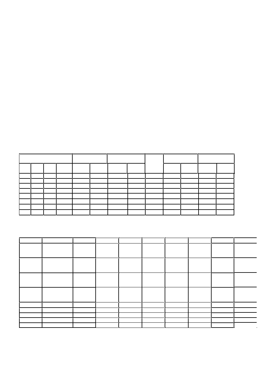
Figure 4: ALU Destination Control
I
2,1,0
O c t a l
0
1
2
3
4
5
6
7
O c t a l
I
5,4,3
ALU Source
/ALU
Function
A,Q
A,B
0,Q
0,B
0,A
D,A
D,Q
D,0
0
Cn=L
R plus S
Cn=H
A+Q
A+Q+1
A+B
A+B+1
Q
Q +1
B
B + 1
A
A + 1
D + A
D + A + 1
D + Q
D + Q + 1
D
D + 1
1
Cn=L
S minus R
Cn=H
Q-A-1
Q-A
B-A-1
B-A
Q -1
Q
B - 1
B
A - 1
A
A - D1
A - D
Q - D - 1
Q - D
-D - 1
- D
2
Cn=L
R minus S
Cn=H
A-Q-1
A-Q
A-B-1
A-B
-Q-1
- Q
- B - 1
- B
- A - 1
- A
D - A -1
D - A
D - Q - 1
D - Q
D - 1
D
3
R or S
A
V
Q
A
V
B
Q
B
A
D
V
A
D
V
Q
D
4
R and S
A
Q
A
B
0
0
0
D
A
D
Q
0
5
RN and S
AN
Q
AN
B
Q
B
A
DN
A
DN
Q
0
6
R EX-OR S
A
Q
A
B
Q
B
A
D
A
D
Q
D
7
R EX NOR S
AN
QN
AN
BN
Q
B
A
DN
AN
DN
QN
DN
+ = plus; - = minus;
V
= OR;
= AND;
= EX-OR
Figure 5: Source Operand and ALU Function Matrix
Microcode
RAM Function
Q-Reg Function
Y
RAM Shifter
Q Shifter
I
8
I
7
I
6
Octal
Code
Shift
Load
Shift
Load
Output
RAM
0
RAM
3
Q
0
Q
3
L
L
L
0
X
None
None
F
Q
F
X
X
X
X
L
L
H
1
X
None
X
None
F
X
X
X
X
L
H
L
2
None
F
B
X
None
A
X
X
X
X
L
H
H
3
None
F
B
X
None
F
X
X
X
X
H
L
L
4
Down
F/2
B
Q/2
Q
F
-
F
0
IN
3
Q
0
IN3
H
L
H
5
Down
F/2
B
X
None
F
F
0
IN
3
Q
0
X
H
H
L
6
Up
2F
B
Up
2Q
Q
F
IN
0
F
3
IN
3
Q
3
H
H
H
7
Up
2F
B
X
None
F
IN
0
F
3
X
Q
3