ChipFind - документация

Электронный компонент: MDS108

Скачать:  PDF   ZIP

Document Outline

1
Zarlink Semiconductor Inc.
Zarlink, ZL and the Zarlink Semiconductor logo are trademarks of Zarlink Semiconductor Inc.
Copyright 2003, Zarlink Semiconductor Inc. All Rights Reserved.
Features
8 10/100 Mbps auto-negotiating RMII ports
1 10/100 Mbps auto-negotiating MII/serial port
(port 8) that can be used as a WAN uplink or as a
9th port
Operates stand-alone or can be cascaded with a
second MDS108 to reach 16 ports
- XLink expansion MII port (port 8)
- Operates at 100/200/300/400 Mbps
External I
2
C EEPROM for power-up configuration
- Default mode allows operation without external
EEPROM
Up to 8 port-based VLANs
Full wirespeed layer 2 switching on all ports (up to
2.679 M packets per second)
Internal 1 K MAC address table
- Auto address learning
- Auto address aging
Leading-edge Quality of Service (QoS)
capabilities provided based on 802.1 p and IP
TOS/DS field
- 2 queues per output port
- Packet scheduling based on Weighted Round
Robin (WRR) and Weighted Random Early
Detection/Drop (WRED)
- With flow control disabled, can drop packets
during congestion using WRED
- 2 levels of packet drop provided
Provides port-based prioritization of packets on
up to 4 ports
- Input ports are defined to be high or low priority
- Allows explicit identification of IP phone ports
Supports both full and half duplex ports
Ports 0 & 1 can be trunked to provide a 200 Mbps
link to another switch or server
Port 7 can be used to mirror traffic from the other 7
ports (0-6)
Utilizes a single low-cost external pipelined,
SyncBurst SRAM (SBRAM) for buffer memory
- 256 KB or 512 KB (1 chip)
Flow control capabilities
- Provides back-pressure for half duplex
- 802.3x flow control for full duplex
Supports external parallel port for configuration
updates
Special power-saving mode for inactive ports
Ability to support WinSock 2.0 and Windows2000
smart applications
Transmit delay control capabilities
- Assures maximum delay (< 1 ms)
- Supports mixed voice/data networks
Optimized pin-out for easy board layout
November 2003
Ordering Information
MDS108AL
208 Pin PQFP
-40
C to +85C
MDS108
Unmanaged 9-Port 10/100 Mbps
Ethernet Switch
Data Sheet
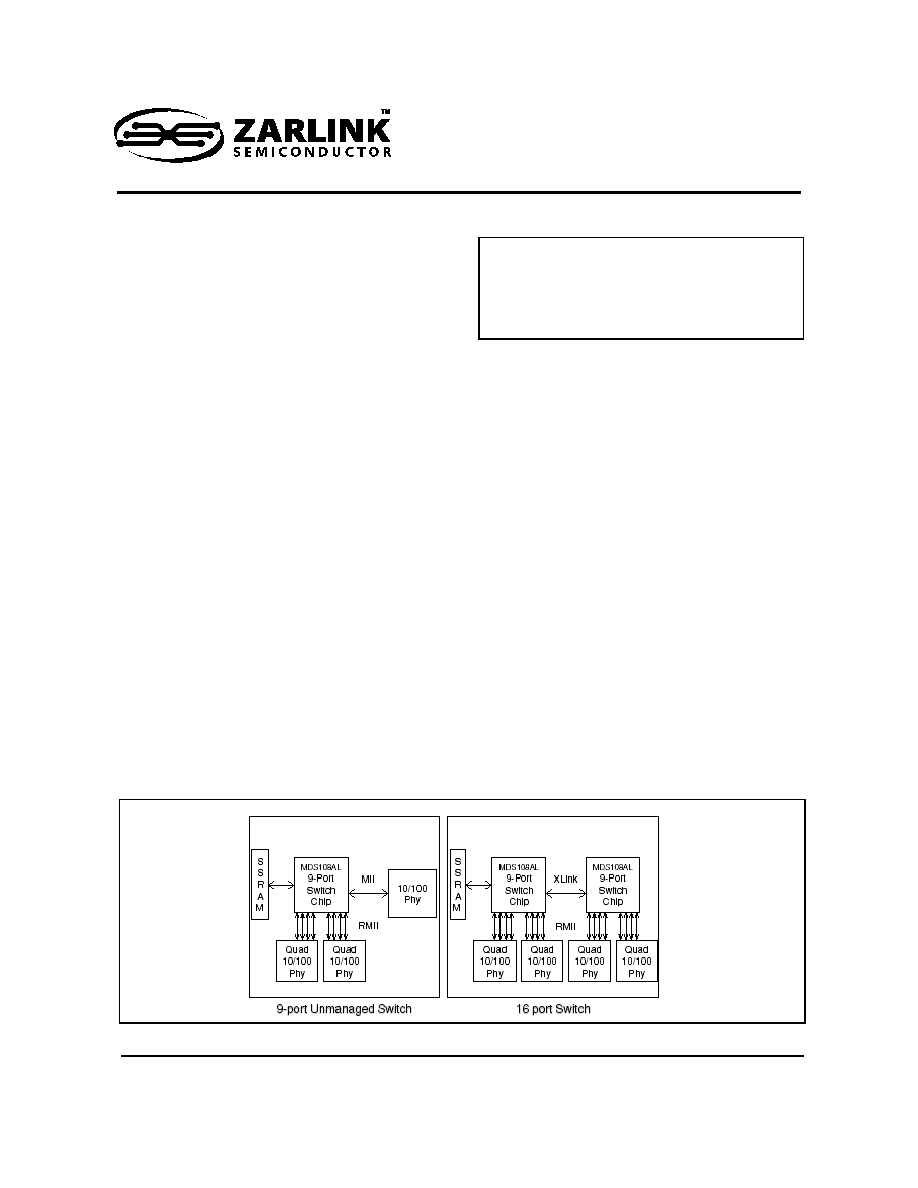
Figure 1 - System Block Diagram
MDS108
Data Sheet
2
Zarlink Semiconductor Inc.
Description
The MDS108 is a fully integrated 9-port Ethernet switch designed to support the low-cost requirements of
unmanaged switch applications. The MDS108 provides features that are normally not associated with plug-and-
play technology, while not requiring an external processor to facilitate their utilization.
The MDS108 begins operating immediately at power-up, learning addresses automatically, and forwarding packets
at full wire-speed to any of its eight output ports or the XLink expansion port. The default configuration allows
operation without using an external EEPROM.
With an EEPROM to configure the device at power-up, the MDS108 provides flexible features: port trunking, port
mirroring, port-based VLANs and (QoS) capabilities that are usually associated only with managed switches.
The built-in intelligence capabilites of the MDS108 allows it to recognize and offer packet prioritization using Zarlink
Semiconductor's QoS. Packets are prioritized based upon their layer 2 VLAN priority tag or the layer 3 Type-Of-
Service/ Differentiated Services (TOS/DS) field. This priority can be defined as transmit and/or drop priority.
The MDS108 can be used to create an 8-port unmanaged switch with one WAN router port by connecting a CPU
(ARM or MPC 850) to the additional MII port (port 8). The only external components needed are the physical layer
transceivers and a single SBRAM, resulting in a low, total system cost.
Designed to support the requirements of converging networks, the MDS108 utilizes a power conserving
architecture. To further enhance this power management, the chip automatically detects when a switch port is not
being utilized, and turns off the logic associated with that port, thereby saving power and reducing the current load
on the switch power supply.
Operating at 66 MHz internally, and with a 66 MHz interface to the external SBRAM, the MDS108 sustains full wire-
speed switching on all 9 ports.
The chip is packaged in a small 208 pin Plastic Quad Flat-Pak (PQFP) package.
MDS108
Data Sheet
3
Zarlink Semiconductor Inc.
MDS108 Physical Pinout
184
186
188
190
192
194
196
198
200
202
204
206
208
74
76
78
12
10
8
6
4
2
72
70
68
66
64
62
60
58
56
54
14
32
30
28
26
24
20
18
16
22
34
52
50
48
46
44
40
38
36
42
NC
NC
NC
NC
NC
VD
D
M4_TXEN M4_TXD[0] M4_TXD[1]
M4_CRS_DV
M4_RXD[0]
M4_RXD[1]
VSS
M5_TXEN
M5_TXD[0] M5_TXD[1]
M5_CRS_DV
M5_RXD[0]
VSS
M6_TXD[0]
M6_TXD[1]
M6_CRS_DV
M6_RXD[0]
M6_RXD[1]
NC
NC
NC
NC
NC
NC
VSS (CORE)
M3_RXD[1]
M3_RXD[0]
M3_CRS_DV
M3_TXD[1]
M3_TXD[0]
M3_TXEN
VDD (CORE)
M2_RXD[1]
M2_RXD[0]
M2_CRS_DV
M2_TXD[1]
M2_TXD[0]
M2_TXEN
VSS
M1_RXD[1]
M1_RXD[0]
M1_CRS_DV
M1_TXD[1]
M1_TXD[0]
M1_TXEN
VDD
M0_RXD[1]
M0_RXD[0]
M0_CRS_DV
M0_TXD[1]
M0_TXD[0]
M0_TXEN
VSS (CORE)
NC
NC
NC
NC
NC
NC
VDD
L_A[13]
L_A[14]
L_A[12]
VSS
L_A[11]
L_A[10]
L_A[9]
VDD_CORE
L_A[8]
L_A[7]
LA_[6]
VSS
L_A[5] L_A[4]
L_A[18]
L_D[31] L_D[30]
L_D[29]
VSS (CORE)
L_D[28]
L_D[27]
L_D[26]
VDD
L_D[25]
L_D[24]
L_D[23]
L_D[22]
VSS
L_D[21]
L_D[20]
L_D[19]
L_D[18]
VDD (CORE)
RMII
Port
Interfaces
182 180 178 176 174 172 170 168 166 164 162 160 158
84
82
80
146
148
150
152
154
156
86
88
90
92
94
96 98 100 102 104
144
126
128
130
132
134
138
140
142
136
124
106
108
110
112
114
118
120
122
116
M7_TXEN
M7_TXD[0]
M7_TXD[1]
M7_CRS_DV
M7_RXD[0]
M7_RXD[1]
VDD
NC
NC
NC
NC
NC
NC
VSS
M_CLK
VDD (CORE)
M8_RXDV
M8_COL
M8_RXCLK
VDD
M8_RXD[0]
M8_RXD[1]
M8_RXD[2]
M8_RXD[3]
VSS (CORE)
M8_TXCLK
VDD
M8_TXEN
M8_TXD[0]
M8_TXD[1]
M8_TXD[2]
M8_TXD[3]
M8_LINK
M8_DUPLEX
M8_REFCLK
VDD
M_MDC
VSS
SCL
TEST#
TRUNK_EN
STROBE
DATA0
ACK
VDD (CORE)
TSTOUT[0]
TSTOUT[1]
TSTOUT[2]
TSTOUT[3]
TSTOUT[4]
TSTOUT[6]
TSTOUT[7]
T_MODE
VSS (CORE)
RSTOUT#
MIR_CTL[0]
MIR_CTL[2]
MIR_CTL[3]
SCLK
VDD
VSS
L_A[2]
L_A[17]
VDD
L_CLK
VSS
L_WE#
L_D[16]
VSS
L_D[14]
L_D[13]
L_D[12]
L_D
[1
1]
VDD L_D[10]
L_D[9]
L_D[8]
VSS (CORE)
L_D
[7]
L_D[6]
L_
D
[
5
]
L_D[4]
VDD
L_D[3]
L_D[1]
L_D[0]
L_A[15]
VDD (CORE)
L_A[16]
L_ADSC#
NC
M6_TXEN
VSS (C
ORE)
VDD (CORE)
L_A[3]
VDD
L_D[17]
L_D[15]
L_D[2]
VSS
L_OE#
MIR_CTL[1]
RSTIN#
TSTOUT[5]
SDA
M_MDIO
VSS
M8_SPEED
Buffer Mem Interface
Co
nfig
I
n
terfaces
RMII Port Interfaces
+
Pin 1 I.D.
M5_RXD[1]
MII Port
Interfaces
MDS108
Data Sheet
4
Zarlink Semiconductor Inc.
Pin Reference Table
Pin #
Pin Name
1
L_A[7]
2
L_A[8]
3
VDD (CORE)
4
L_A[9]
5
L_A[10]
6
L_A[11]
7
VSS
8
L_A[12]
9
L_A[13]
10
L_A[14]
11
VDD
12
NC
13
NC
14
NC
15
NC
16
NC
17
NC
18
VSS (CORE)
19
M0_TXEN
20
M0_TXD[0]
21
M0_TXD[1]
22
M0_CRS_DV
23
M0_RXD[0]
24
M0_RXD[1]
25
VDD
26
M1_TXEN
27
M1_TXD[0]
28
M1_TXD[1]
29
M1_CRS_DV
30
M1_RXD[0]
31
M1_RXD[1]
32
VSS
33
M2_TXEN
34
M2_TXD[0]
35
M2_TXD[1]
36
M2_CRS_DV
37
M2_RXD[0]
38
M2_RXD[1]
39
VDD (CORE)
40
M3_TXEN
41
M3_TXD[0]
42
M3_TXD[1]
43
M3_CRS_DV
44
M3_RXD[0]
45
M3_RXD[1]
46
VSS (CORE)
47
NC
48
NC
49
NC
50
NC
51
NC
52
NC
53
NC
54
NC
55
NC
56
NC
57
NC
58
NC
59
VDD
60
M4_TXEN
61
M4_TXD[0]
62
M4_TXD[1]
63
M4_CRS_DV
64
M4_RXD[0]
65
M4_RXD[1]
66
VSS
67
M5_TXEN
68
M5_TXD[0]
69
M5_TXD[1]
70
M5_CRS_DV
71
M5_RXD[0]
72
M5_RXD[1]
73
VDD (CORE)
74
M6_TXEN
75
M6_TXD[0]
76
M6_TXD[1]
77
M6_CRS_DV
78
M6_RXD[0]
79
M6_RXD[1]
80
VSS (CORE)
81
M7_TXEN
82
M7_TXD[0]
83
M7_TXD[1]
84
M7_CRS_DV
85
M7_RXD[0]
86
M7_RXD[1]
87
VDD
88
NC
89
NC
90
NC
91
NC
92
NC
93
NC
94
VSS
95
M_CLK
96
VDD (CORE)
97
M8_RXDV/S8_CRS_DV
98
M8_COL/S8_COL
99
VSS
100
M8_RXCLK/S8_RXCLK
101
VDD
102
M8_RXD[0]/S8_RXD
103
M8_RXD[1]
104
M8_RXD[2]
105
M8_RXD[3]
106
VSS (CORE)
MDS108
Data Sheet
5
Zarlink Semiconductor Inc.
107
M8_TXCLK/S8_TXCLK
108
VDD
109
M8_TXEN[0]/S8_TXEN
110
M8_TXD[0]/S8_TXD
111
M8_TXD[1]
112
M8_TXD[2]
113
M8_TXD[3]
114
M8_LINK/S8_LINK
115
M8_DUPLEX/S8_DUPL
EX
116
M8_SPEED
117
VSS
118
M8_REFCLK
119
VDD
120
M_MDC
121
VSS
122
M_MDIO
123
SCL
124
SDA
125
TEST#
126
TRUNK_ENABLE
127
STROBE
128
DATA0
129
ACK
130
VDD (CORE)
131
TSTOUT[0]
132
TSTOUT[1]
133
TSTOUT[2]
134
TSTOUT[3]
135
TSTOUT[4]
136
TSTOUT[5]
137
TSTOUT[6]
138
TSTOUT[7]
139
T_MODE
140
VSS (CORE)
141
RSTOUT#
142
RSTIN#
143
MIRROR_CONTROL[0]
144
MIRROR_CONTROL[1]
145
MIRROR_CONTROL[2]
146
MIRROR_CONTROL[3]
147
VDD
148
SCLK
149
VSS
150
L_A[2]
151
L_A[17]
152
VDD
153
L_CLK
154
VSS
155
L_WE#
156
L_OE#
157
L_ADSC#
158
L_A[16]
159
VDD (CORE)
160
L_A[15]
161
L_D[0]
162
VSS
163
L_D[1]
164
L_D[2]
165
L_D[3]
166
VDD
167
L_D[4]
168
L_D[5]
169
L_D[6]
170
L_D[7]
171
VSS (CORE)
172
L_D[8]
173
L_D[9]
174
L_D[10]
175
VDD
176
L_D[11]
177
L_D[12]
178
L_D[13]
179
L_D[14]
180
VSS
181
L_D[15]
182
L_D[16]
183
L_D[17]
184
VDD (CORE)
185
L_D[18]
186
L_D[19]
187
L_D[20]
188
L_D[21]
189
VSS
190
L_D[22]
191
L_D[23]
192
L_D[24]
193
L_D[25]
194
VDD
195
L_D[26]
196
L_D[27]
197
L_D[28]
198
VSS (CORE)
199
L_D[29]
200
L_D[30]
201
L_D[31]
202
VDD
203
L_A[18]
204
L_A[3]
205
L_A[4]
206
L_A[5]
207
VSS
208
L_A[6]