1
MF431
High Performance LED
Description
This device is designed for FDDI and ATM 155 Mbps
applications and offers an excellent price/
performance ratio for cost-effective solutions. Its
double-lens optical system results in optimum
coupling of power into the fiber.
DS5470
ISSUE 1
May 2001
Ordering Information
MF431
13429.11 TO-46 Package
MF431 ST
13324.11 ST Housing
MF431 SC
13591.11 SC Housing
MF431 SMA
13548.11 SMA Housing
MF431 FC
13549.11 FC Housing
Note: Rated Fiber coupled power apply only on the TO-46 package,
for housing options fiber coupled power is typically 10% less
Optical and Electrical Characteristics - Case temperature 25�C
Parameter
Symbol
Min.
Typ.
Max.
Unit
Test Condition
Fiber-Coupled Power
(Fig. 1,2 & 3) (Table 1)
P
fiber
43
�
W
I
F
=60mA
(Note 1)
Fiber:
62.5/
125
�
m
Graded
Index
Rise and Fall Time
(10-90%)
t
r'
t
f
2.5
ns
I
F
=60mA
(no bias)
Bandwidth
(3dB
el
)
f
c
125
MHz
I
F
=60mA
Peak Center Wavelength
p
1320
nm
I
F
=60mA
Spectral Width (FWHM)
135
nm
I
F
=60mA
Forward Voltage (Fig. 5)
V
F
1.3
1.65
V
I
F
=60mA
Reverse Current
I
R
100
�
A
V
R
=1V
Capacitance
C
200
pF
V
R
=0V, f=1 MHz
Note 1: Measured at the exit of 100 meters of fiber
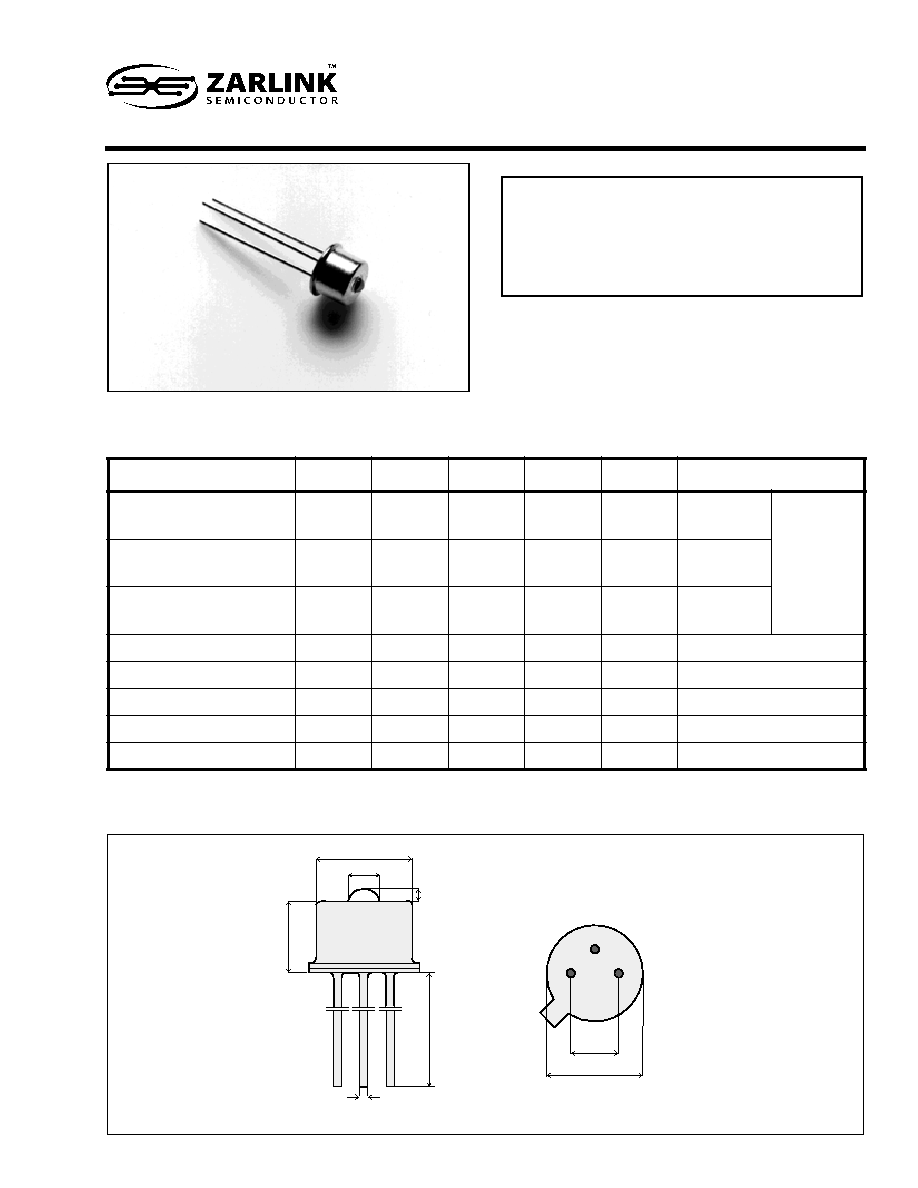
TO-46 Package with Lens
0.6
14
�1.5
�4.7
3.7
0.4
5.4
2.5
CASE
ANODE
CATHODE
BOTTOM VIEW
The diode chip is isolated from the case
All dimensions in mm
MF431
2
Absolute Maximum Ratings
Thermal Characteristics
Parameter
Symbol
Limit
Storage Temperature
T
stg
-55 to +125�C
Operating Temperature see (derating: Fig. 4)
T
op
-40 to +85�C
Electrical Power Dissipation (derating: Fig. 4)
P
tot
160 mW
Continuous Forward Current (f<10kHz)
I
F
80 mA
Peak Forward Current (duty cycle<50%, f>1MHz)
I
FRM
130 mA
Reverse Voltage
V
R
0.5V
Soldering Temperature (2mm from the case for 10sec)
T
sld
260�C
Parameter
Symbol
Min.
Typ.
Max.
Unit
Thermal Resistance - Infinite Heat Sink
R
thjc
150
�C/W
Thermal Resistance - No Heat Sink
R
thja
400
�C/W
Temperature Coefficient - Optical Power
dP/dT
j
-0.75
%/�C
Temperature Coefficient - Wavelength
/dT
j
0.45
nm/�C
BOTTOM VIEW ( 10 : 1 )
SIDE VIEW
� Zarlink Semiconductor 2002. All rights reserved.
ISSUE
ACN
DATE
APPRD.
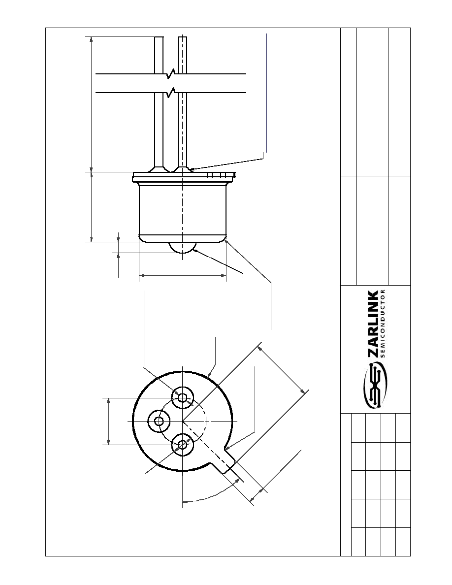
Previous package codes
Title
Drawing type
Package code
1
JS004 076R1 A
22-MAR-03
TD/BE
JS004076
Package drawing, TO-46 with lens
TB
2,54
0,45
n
- 0,04
0,03
+
(3x)
1,17
n
- 0
0,05
+
(3x)
1,0
2
`
0,3
3,
6
45�
R0,2 max (4x)
R2,7
4
,
7
n
0,6
3,8
13,46
`
0,76
Lens
n
1.5
`
0.05
R0,4 max
0,3 max glass overmould (2x)
NOTES:-
1. All dimensions in mm.
2. General tol. ISO-2768-mK.
3. Coating:
Case: Ni 1,5-2,5 �m.
Header: Ni 2-3 �m / Au min 1,32 �m.

www.zarlink.com
Information relating to products and services furnished herein by Zarlink Semiconductor Inc. trading as Zarlink Semiconductor or its subsidiaries (collectively
"Zarlink") is believed to be reliable. However, Zarlink assumes no liability for errors that may appear in this publication, or for liability otherwise arising from the
application or use of any such information, product or service or for any infringement of patents or other intellectual property rights owned by third parties which may
result from such application or use. Neither the supply of such information or purchase of product or service conveys any license, either express or implied, under
patents or other intellectual property rights owned by Zarlink or licensed from third parties by Zarlink, whatsoever. Purchasers of products are also hereby notified
that the use of product in certain ways or in combination with Zarlink, or non-Zarlink furnished goods or services may infringe patents or other intellectual property
rights owned by Zarlink.
This publication is issued to provide information only and (unless agreed by Zarlink in writing) may not be used, applied or reproduced for any purpose nor form part
of any order or contract nor to be regarded as a representation relating to the products or services concerned. The products, their specifications, services and other
information appearing in this publication are subject to change by Zarlink without notice. No warranty or guarantee express or implied is made regarding the
capability, performance or suitability of any product or service. Information concerning possible methods of use is provided as a guide only and does not constitute
any guarantee that such methods of use will be satisfactory in a specific piece of equipment. It is the user's responsibility to fully determine the performance and
suitability of any equipment using such information and to ensure that any publication or data used is up to date and has not been superseded. Manufacturing does
not necessarily include testing of all functions or parameters. These products are not suitable for use in any medical products whose failure to perform may result in
significant injury or death to the user. All products and materials are sold and services provided subject to Zarlink's conditions of sale which are available on request.
Purchase of Zarlink's I
2
C components conveys a licence under the Philips I
2
C Patent rights to use these components in an I
2
C System, provided that the system
conforms to the I
2
C Standard Specification as defined by Philips.
Zarlink, ZL and the Zarlink Semiconductor logo are trademarks of Zarlink Semiconductor Inc.
Copyright 2003, Zarlink Semiconductor Inc. All Rights Reserved.
TECHNICAL DOCUMENTATION - NOT FOR RESALE
For more information about all Zarlink products
visit our Web Site at
