1
MF446
High-Performance PIN
Description
The very high speed and low capacitance of this
GaAs PIN Photodiode makes it ideal for datacom and
general purpose applications. Its double-lens optical
system collects power from fibers with up to 100mm
without loss in responsivity and a reverse voltage of
only 3.3 Volts makes interfacing to a preamplifier
easy.
DS5461
ISSUE 1
May 2001
Ordering Information
MF446
13514.11 TO-46 Package
MF446 ST
15062.11 ST Housing
MF446 SMA
13743.11 SMA Housing
MF446 FC
13741.11 FC Housing
MF446 SC
15268.11 SC Housing
MF446 PT
15050.11 Pig-Tail including 1m of
62.5/125
�
m multi-mode fibre
Note: The rated Responsivity applies to all options.
Optical and Electrical Characteristics - Case Temperature -40 to +85�C
Parameter
Symbol
Min.
Typ.
Max.
Unit
Test Condition
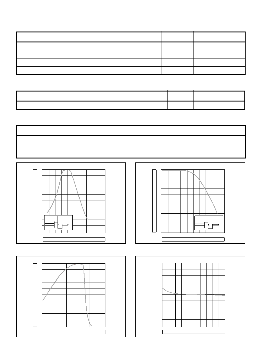
Responsivity
(Fig. 1 & 2) (Table 1)
R
0.35
0.45
A/W
V
R
=3.3V,
5V
=850nm
Fiber:
62.5/
125
�
m
Graded
Index
NA=0.275
Bandwidth
c
1.5
GHz
V
R
=3.3V,
5V
R
L
=50
Capacitance (Fig. 4)
C
0.8
pF
V
R
=3.3V, 5V, f=1MHz
Dark Current
I
d
0.4
nA
V
R
=3.3V, 5V
TO-46 Package with Lens
0.6
14
�1.5
�4.7
3.7
0.4
5.4
2.5
CATHODE
ANODE
CASE
BOTTOM VIEW
All dimensions in mm
The diode chip is isolated from the case

BOTTOM VIEW ( 10 : 1 )
SIDE VIEW
� Zarlink Semiconductor 2002. All rights reserved.
ISSUE
ACN
DATE
APPRD.
Previous package codes
Title
Drawing type
Package code
1
JS004 076R1 A
22-MAR-03
TD/BE
JS004076
Package drawing, TO-46 with lens
TB
2,54
0,45
n
- 0,04
0,03
+
(3x)
1,17
n
- 0
0,05
+
(3x)
1,0
2
`
0,3
3,
6
45�
R0,2 max (4x)
R2,7
4
,
7
n
0,6
3,8
13,46
`
0,76
Lens
n
1.5
`
0.05
R0,4 max
0,3 max glass overmould (2x)
NOTES:-
1. All dimensions in mm.
2. General tol. ISO-2768-mK.
3. Coating:
Case: Ni 1,5-2,5 �m.
Header: Ni 2-3 �m / Au min 1,32 �m.

www.zarlink.com
Information relating to products and services furnished herein by Zarlink Semiconductor Inc. trading as Zarlink Semiconductor or its subsidiaries (collectively
"Zarlink") is believed to be reliable. However, Zarlink assumes no liability for errors that may appear in this publication, or for liability otherwise arising from the
application or use of any such information, product or service or for any infringement of patents or other intellectual property rights owned by third parties which may
result from such application or use. Neither the supply of such information or purchase of product or service conveys any license, either express or implied, under
patents or other intellectual property rights owned by Zarlink or licensed from third parties by Zarlink, whatsoever. Purchasers of products are also hereby notified
that the use of product in certain ways or in combination with Zarlink, or non-Zarlink furnished goods or services may infringe patents or other intellectual property
rights owned by Zarlink.
This publication is issued to provide information only and (unless agreed by Zarlink in writing) may not be used, applied or reproduced for any purpose nor form part
of any order or contract nor to be regarded as a representation relating to the products or services concerned. The products, their specifications, services and other
information appearing in this publication are subject to change by Zarlink without notice. No warranty or guarantee express or implied is made regarding the
capability, performance or suitability of any product or service. Information concerning possible methods of use is provided as a guide only and does not constitute
any guarantee that such methods of use will be satisfactory in a specific piece of equipment. It is the user's responsibility to fully determine the performance and
suitability of any equipment using such information and to ensure that any publication or data used is up to date and has not been superseded. Manufacturing does
not necessarily include testing of all functions or parameters. These products are not suitable for use in any medical products whose failure to perform may result in
significant injury or death to the user. All products and materials are sold and services provided subject to Zarlink's conditions of sale which are available on request.
Purchase of Zarlink's I
2
C components conveys a licence under the Philips I
2
C Patent rights to use these components in an I
2
C System, provided that the system
conforms to the I
2
C Standard Specification as defined by Philips.
Zarlink, ZL and the Zarlink Semiconductor logo are trademarks of Zarlink Semiconductor Inc.
Copyright 2003, Zarlink Semiconductor Inc. All Rights Reserved.
TECHNICAL DOCUMENTATION - NOT FOR RESALE
For more information about all Zarlink products
visit our Web Site at