
1
MGCR01
Dual Mode IF Receiver for TDMA/AMPS and CDMA/AMPS
Datasheet
DS4721
ISSUE 4.4
November 2001
Ordering Information
MGCR01/KG/QP1S
MGCR01/KG/QP1T
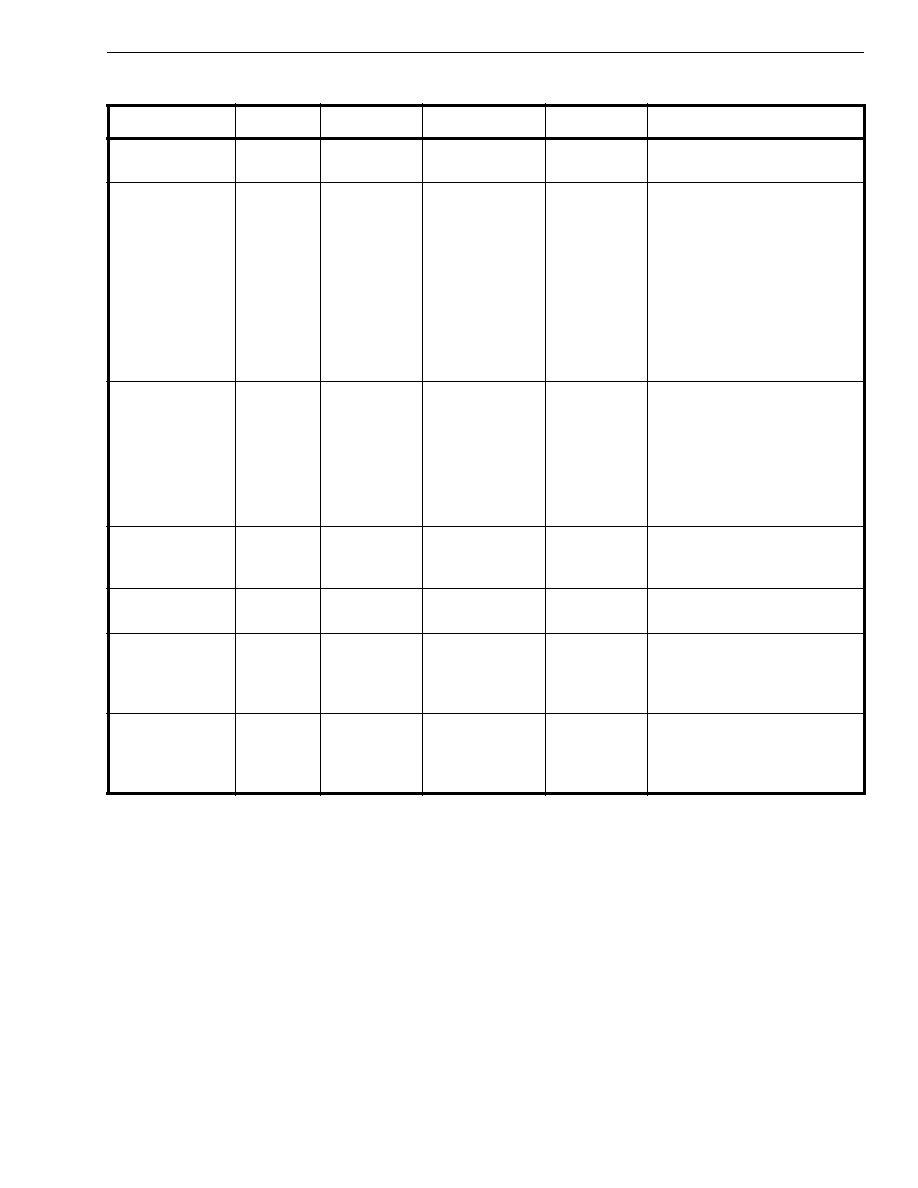
and differential I and Q baseband outputs. The
MGCR01 interfaces directly with MGCM01 for
TDMA/AMPS (using 60kHz low IF) and MGCM03 or
MGCM04 for CDMA and AMPS applications. The on
chip oscillator and prescaler are also compatible with
the PLL synthesisers on these devices.
Figure 1 - Block Diagram
Features
∑
Dual IF Inputs 50 to 250 MHz
∑
90dB AGC Gain Control
∑
IQ demodulator
∑
On chip oscillator provides high accuracy
quadrature LO generation
∑
Optional IF Output
∑
3 Volt Power Supply
∑
28 lead QSOP Package
Description
The MGCR01 is designed for use in dual mode
mobile phones (TDMA/AMPS and CDMA/AMPS).
The circuit provides IF amplification with gain control
Temperature
Comp.
DLL
I OUT
IF OUT
FM IFIN
Q OU T
Gain
Control
Mode
Control
CDMA IFIN
AGC
STARTUP
ENABLE
MODE CDM
VHF B
U
F
VHF RES
PRESCALER
Overload
Indicator
O
VERLO
AD DET
BAND 1900
VHF VCC
VHF VEE
IF VCC
IF VEE
DIV2 EN

MGCR01
2
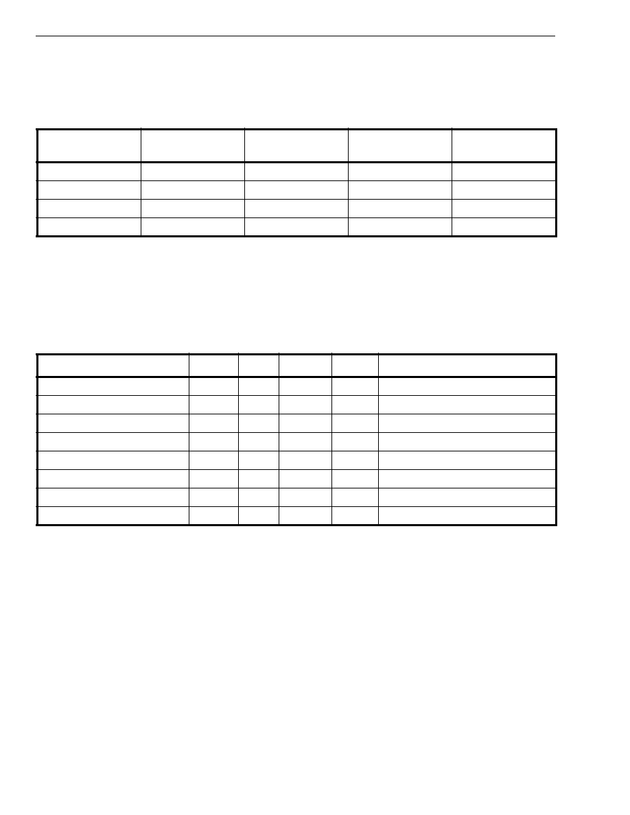
Pin No.
Pin Name
Description
1
IF VCC
Supply for IF inputs and AGC blocks
2
IF OUTB
IF ouput
3
IF OUT
IF output
4
IF VEE
Ground for IF inputs and AGC blocks
5
GND
Substrate ground
6
CDMA IFIN
IF input (CDMA)
7
CDMA IFINB
IF input (CDMA)
8
FM IFIIN
IF input (FM)
9
FM IFINB
IF inputs (FM) (AC ground)
10
AGC
AGC Control for IF section
11
AGCB
AGC control for IF sections (AC ground)
12
MODE CDMA
CDMA/FM input select
13
ENABLE
Power up AGC sections of device
14
GND
Substrate Ground
15
STARTUP
Power up Oscillator, DLL and Mixer
16
QOUTB
Q channel baseband output
17
QOUT
Q channel baseband output
18
GND
Ground
19
VHF BUFB
VHF oscillator buffered output for synthesiser
20
VHF BUF
VHF oscillator buffered output for synthesiser
21
BAND 1900
VHF oscillator mode (see table 1)
22
VHF RESB
VHF VCO resonator
23
VHF RES
VHF VCO resonator
24
OVERLOAD DET
Overload detector output
25
VHF VEE
Ground for VHF VCO and DLL blocks
26
I OUT
I channel baseband output
27
I OUTB
I channel baseband output
28
VHF VCC
Supply for VHF and DLL blocks
Table 1 - Pin Description
Figure 2 - Pin Connections
IF VCC
IF OUTB
IF OUT
IF VEE
GND
CDMA IFIN
CDMA IFINB
FM IFIN
FM IFINB
AGC
AGCB
MODE CDMA
ENABLE
GND
VHF VCC
I OUTB
I OUT
VHF VEE
OVERLOAD DET
VHF RES
VHF RESB
BAND 1900
VHF BUF
VHF BUFB
DIV2 EN
Q OUT
Q OUTB
STARTUP
QSOP28
MGCR01
3
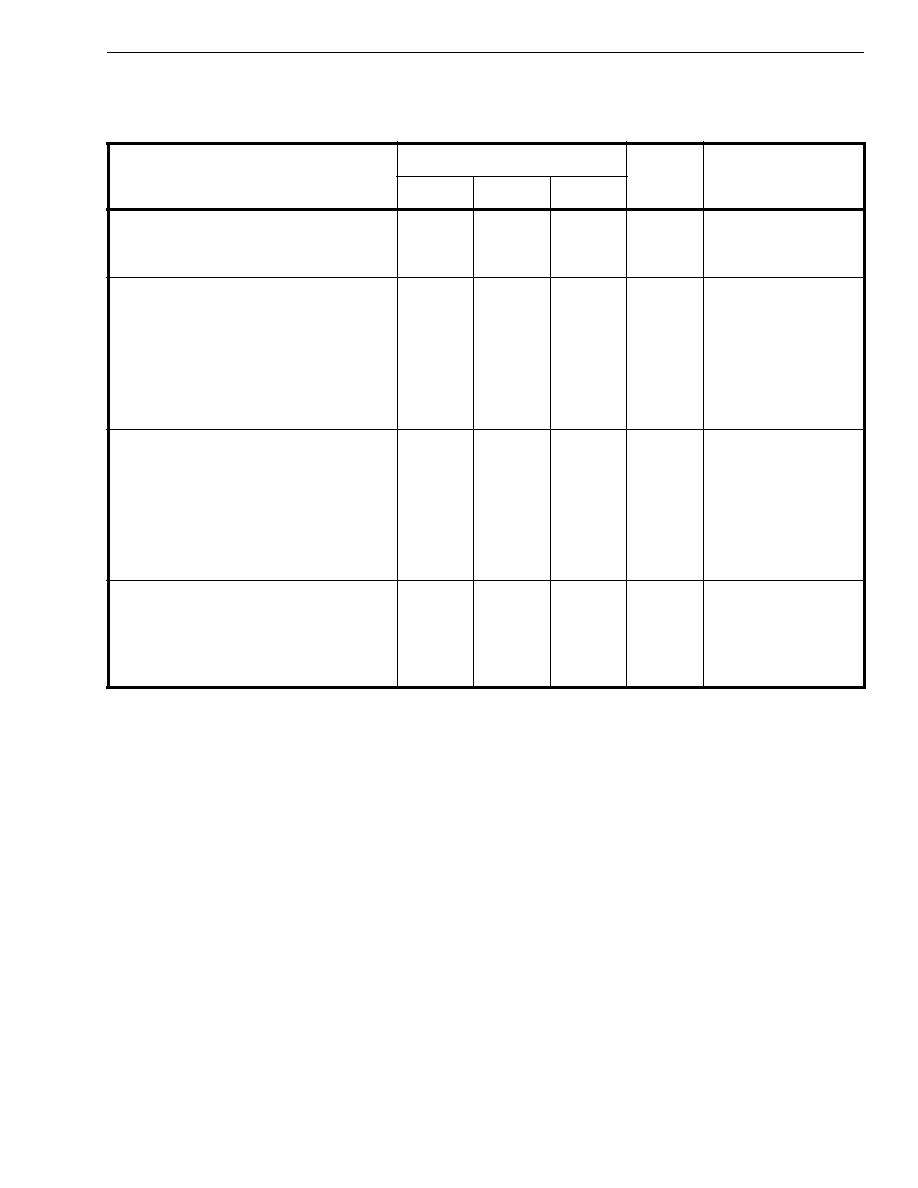
X = Don't Care
Notes:
1. STARTUP mode is provided to allow VCO/DLL/prescalers to stabilise before signal path is activated.
This is a power-saving feature since the signal path is redundant during this period. If this feature is not
required, the ENABLE and STARTUP control pins can be shorted together so that all circuitry is activated
at the same time.
2. In high band mode (Band 1900 = 1) the VCO operates at twice the IF frequency. For example if IF =
210.38MHz then the oscillator operates at 420.76MHz. A delay locked loop (DLL) circuit then generates the
quadrature LO signals.
3. In low band mode (Band 1900 = 0) the VCO operates at 4 times the IF frequency. for example if IF =
85.38MHz the oscillator operates at 341.52MHz. This is then divided and uses DLL circuit to provide the
quadrature LO signals.
4. This mode can be used for FM. The VCO operates at twice the LO frequency. This mode is not normally
used as a large tuning range is required on the VCO.
Description
ENABLE
STARTUP
MODE CDMA
BAND 1900
Conditions
Standby Mode
0
0
X
X
All circuits powered down
except logic inputs
Start up Mode
0
0
1
1
X
X
1
0
For high band IF
For low band IF
Turns on VCO circuits, DLL
quadrature generation,
prescaler and IQ
demodulator. All other
circuits remain powered
down
CDMA mode
1
1
1
1
1
1
1
0
For high band IF
For low band IF
All circuits operational
except for IF output buffer,
CDMA input stage selected.
FM Mode
1
1
0
0
All circuits operational
except for IF output buffer,
FM input stage selected.
Alternative FM
mode
1
1
0
1
Note 4
CDMA IF AGC
only mode
1
0
1
X
Demodulator and LO
generation circuitry powered
down. IF output buffer
enabled
FM IF AGC
1
0
0
X
Demodulator and LO
generation circuitry powered
down. IF output buffer
enabled.
Table 2 - Electrical Characteristics (Mode Control)
MGCR01
4
DLL and Prescaler divide ratios
The BAND 1900 and DIV2 EN inputs allow the overall divide ratio to control the total divide ratio in MGCR01 as
shown in the following table.
Notes:
if DIV2 EN is set low then the total divider ratio is always 8.
If DIV2 EN is set high then the prescaler divide ratio is always 2. For example with BAND 1900 high and if the
oscillator frequency is 300MHz, then the DLL output (the mixer LO frequency) will be 150MHz and the
prescaler output will be 75MHz.
Electrostatic handling precautions must be applied.
BAND 1900
DIV2 EN
DLL Divide Ratio
Prescaler Divide
Ratio
Total Divide Ratio
1
1
2
2
4
0
1
4
2
8
1
0
2
4
8
0
0
4
2
8
Table 3 - Prescaler Ratios
Description
Min
Typ
Max
Units
Comments
Supply Voltage
4.0
Volts
Operation temperature, Tamb
-30
+100
∞C
Ambient temperature
Storage temperature, Tstg
-40
+125
∞C
Junction temperature, Tj
+150
∞C
Power dissipation
350
mW
Maximum Pin Voltage
Vcc+0.6
Volts
All pins except V
CC
and GND
Minimum Pin Voltage
-0.6
Volts
All pins except V
CC
and GND
ESD voltage
1.75
kV
Human Body Metal
Table 4 - Absolute Maximum Ratings
MGCR01
5
T
amb
= 30∞C to +70∞C, V
CC
= +2.7 to +3.6. These characteristics are guaranteed by either production test or
design. They apply within the specified ambient temperature and supply voltage unless otherwise stated.
Notes:
1. Specifications are guaranteed over -30 to + 70∞C, however operation is guaranteed over the extended
range of -30 to +85∞C with minimal variation in specified parameters.
Characteristic
Value
Units
Conditions
Min
Typ
Max
General
Supply Voltage
Operating Temperature
2.7
-30
3.0
27
3.6
85
V
∞C
All V
CC
Pins
Ambient See note 1
Current Consumption
Standby Mode
Startup Mode
CDMA Mode
FM Mode
CDMA AGC only Mode
FM AGC only Mode
0.03
8
14
14
8
11
0.1
13
23
23
13
18
mA
mA
mA
mA
mA
mA
Mode Control Logic
CMOS input logic high, VIH
CMOS input high current, IIH
CMOS input low current, IIL
Switching time between any two modes
AGC Control
AGC Input impedance
V
CC
-0.5
-10
-10
0.1
100
3
130
V
CC
+0.1
10
10
2.6
160
V
µ
A
µ
A
ms
V
k
All logic inputs
All logic inputs
All logic inputs
DC Common Mode voltages
I OUT, I OUTB (CDMA Mode)
I OUTB, QOUTB
I OUT<Q OUT (FM Mode)
I OUTB, Q OUTB
V
CC
-0.8
V
CC
-0.8
V
CC
-0.6
V
CC
-0.6
V
CC
-0.4
V
CC
-0.4
V
V
Table 5 - Electrical Characteristics (DC specifications)