1
MT312
Satellite Channel Decoder
Design Manual
DM5651
ISSUE 1.2
January 2002
Ordering Information
MT312C/CG/GP1N
The MT312 is a QPSK/BPSK 1 to 45MBaud
demodulator and channel decoder for digital satellite
television transmissions to the European Broadcast
Union ETS 300 421 specification (ref. 1). It receives
analogue I and Q signals from the tuner, digitises
and digitally demodulates this signal, and
implements the complete DVB/DSS FEC (Forward
Error Correction), and de-scrambling function. The
output is in the form of MPEG2 or DSS transport
stream data packets. An external MPEG clock input
is provided for synchronisation to MPEG decoders
and DVB Common Interface Modules. The MT312
also provides automatic gain control to the RF front-
end devices.
The MT312 has a serial 2-wire bus interface to the
control microprocessor. Minimal software is required
to control the MT312 because of the built in
automatic search and decode control functions.
Figure 1 - System Block Diagram - SNIM5
Key Features
�
Conforms to EBU specification for DVB-S and
DirecTV specification for DSS.
�
On-chip digital filtering supports 1 to 45MBaud
Symbol rates.
�
On-chip 6-bit 60 or 90MHz dual-ADC.
�
High speed scanning mode for blind symbol
rate/code rate acquisition.
�
Automatic IQ phase resolution.
�
No signal indicator.
�
Up to �15MHz LNB frequency tracking.
�
Fully digital timing and phase recovery loops.
�
High level software interface for minimum
development time.
�
DiSEqCTM v2.2: receive/transmit for full control
of LNB and dish.
Applications
�
DVB 1 to 45MBaud compliant satellite
receivers.
�
DSS 20MBaud compliant satellite receivers.
�
SCPC receivers. (Single Channel Per Carrier)
�
SMATV trans-modulators. (Single Master
Antenna TV)
�
LMDS (Local Multipoint Distribution Service)
�
Satellite PC applications.
I
Q
2-wire bus control
Synthesiser
SP5769
Tank
2-wire bus
control
Transport
stream O/P
Channel
Decoder
MT312
Low pass
Filter
Direct
Conversion
Tuner
SL1925
AGC
AMP
SL1914
AGC control
I I/P
Q I/P
RF I/P
Supersedes DS5347 Issue 1.2 November 2001

MT312
Design Manual
2
PIN
FUNCTION
PIN
FUNCTION
PIN
FUNCTION
PIN
FUNCTION
1
CVSS
21
PLLVDD
41
CVSS
61
MDO[1]
2
CVDD
22
PLLGND
42
CVDD
62
CVDD
3
IIN[1]
23
PLL1
43
AGC
63
MDO[2]
4
ADDR[7]
24
ADCFGND
44
CLK2/GPP0
64
MDO[3]
5
ADDR[6]
25
ADCFVDD
45
DATA2/GPP1
65
MDO[4]
6
ADDR[5]
26
VRT
46
DISEQC2/GPP2
66
MDO[5]
7
ADDR[4]
27
IREF
47
DISEQC1 HV
67
CVDD
8
ADDR[3]
28
ISINGP
48
DISEQC0 22kHz
68
MDO[6]
9
CVDD
29
NC
49
RESET
69
MDO[7]
10
CVSS
30
ADCDVDD
50
CVDD
70
CVSS
11
ADDR[2]
31
ADCDGND
51
CVSS
71
MDOEN
12
ADDR[1]
32
VRM
52
STATUS
72
MOVAL
13
VDD
33
QSINGP
53
CLK1
73
VDD
14
MICLK
34
QREF
54
DATA1
74
VSS
15
VSS
35
VRB
55
CVDD
75
BKERR
16
TESTCLK
36
ADCAGND
56
VSS
76
MOSTRT
17
CVDD
37
ADCAVDD
57
IRQ
77
IIN[5]
18
XTI
38
RREF
58
MOCLK
78
IIN[4]
19
XTO
39
TEST1
59
MDO[0]
79
IIN[3]
20
CVSS
40
TEST2
60
CVSS
80
IIN[2]
Table 1 - MT312 pin-out
1
80
61
20
21
40
41
60
Figure 2 - System Block Diagram - SNIM5

Design Manual
MT312
3
Quick start overview
The MT312 is a QPSK/BPSK 1 to 45MBaud
demodulator and channel decoder for digital satellite
television transmissions compliant to both DVB-S
and DSS standards and other systems, such as
LMDS, that use the same architecture.
A Command Driven Control (CDC) system is
provided making the MT312 very simple to program.
After the tuner has been programmed to the required
frequency, to acquire a DVB transmission, the
MT312 requires a minimum of five registers to be
written. Activity flow diagrams for initialisation and
basic channel change are included in section 2.
The MT312 provides a monitor of Bit Error Rate after
the QPSK module and also after the Viterbi module.
For receiver installation, a high speed scan or 'blind
search' mode is available. This allows all signals
from a given satellite to be evaluated for frequency,
symbol rate and convolutional coding scheme. The
phase of the IQ signals can be automatically
determined.
Full DiSEqCTM v2.2 is provided for both writing and
reading DiSEqCTM messages. Storage in registers
for up to eight data bytes sent and eight data bytes
received is provided.
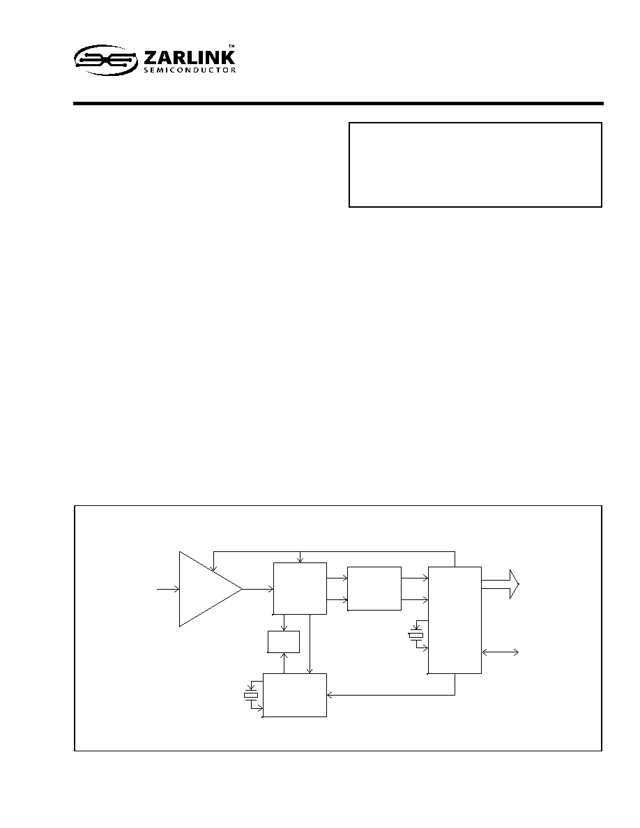
Figure 3 - MT312 Functional Block Diagram
Analog
AG
Ccontrol
Dual ADC
De-rotator
Decimation
Filteriing
Timing recovery
Matched filter
Phase recovery
DVB
DSS
FEC
Clock Generation
Acquisition
Control
I?C
Interface
Bus I/O
MPEG/
DSS
Packets
I I/P
Q I/P
Additional Features
�
2-wire bus microprocessor interface.
�
All digital clock and carrier recovery.
�
On-chip PLL clock generation using low cost 10
to 15MHz crystal.
�
3.3V operation.
�
80 pin MQFP package.
�
Low external component count.
�
Commercial temperature range 0 to 70�C.
Demodulator
�
BPSK or QPSK programmable.
�
Optional fast acquisition mode for low symbol
rates.
Viterbi
�
Programmable decoder rates 1/2, 2/3, 3/4, 5/6,
6/7, 7/8.
�
Automatic spectrum resolution of IQ phase.
�
Constraint length k=7.
�
Trace back depth 128.
�
Extensive SNR and BER monitors.
De-Interleaver
�
Compliant with DVB and DSS standards.
Reed Solomon
�
(204, 188) for DVB and (146,130) for DSS.
�
Reed Solomon Bit-error-rate monitor to indicate
Viterbi performance.
De-Scrambler
�
EBU specification De-scrambler for DVB mode.
Outputs
�
MPEG transport parallel & serial output.
�
MPEG clock input for external synchronising of
MPEG data output.
�
Integrated MPEG2 TEI bit processing for DVB
only.
Application Support
�
Channel decoder system evaluation board.
�
Windows based evaluation software.
�
ANSI C generic software.

MT312
Contents
4
Contents
1
Functional Overview ............................................................................................. 10
1.1 Introduction
........................................................................................................................................ 10
1.2
Analogue-to-Digital Converter ............................................................................................................ 10
1.3 QPSK
Demodulator
............................................................................................................................ 10
1.4
Forward Error Correction .................................................................................................................. 11
1.4.1.1
Viterbi Error Count Measurement ................................................................................................ 11
1.4.1.2
Viterbi Error Count Coarse Indication .......................................................................................... 12
1.4.2
The Frame Alignment Block ........................................................................................................ 12
1.4.3
The De-interleaver Block ............................................................................................................. 13
1.4.3.1 DVB
............................................................................................................................................. 13
1.4.3.2 DSS
............................................................................................................................................. 13
1.4.4
The Reed Solomon Decoder Block ............................................................................................. 14
1.4.5
The Energy Dispersal (De-Scrambler) Block, DVB only .............................................................. 14
1.4.6 Output
Stage
............................................................................................................................... 15
1.5 Control
................................................................................................................................................ 15
1.5.2
Symbol Rate and Code Rate Search Mode ................................................................................ 16
1.6
Direct Conversion Application ............................................................................................................ 16
1.7 DiSEqCTM Transmit and Receive Messages ..................................................................................... 17
1.7.1 DiSEqCTM Transmitting Messages .............................................................................................. 17
1.7.2 DiSEqCTM Receiving Messages .................................................................................................. 17
2
MT312 Software Control ....................................................................................... 18
2.1
MT312 Register Map Overview .......................................................................................................... 18
3 MT312
Initialisation
............................................................................................... 19
3.1
The Configuration Register (127) ....................................................................................................... 19
3.2
Power Supplies ................................................................................................................................... 19
3.3 Initialisation
Sequence
....................................................................................................................... 20
3.4 Spectral
Inversion
.............................................................................................................................. 21
3.5
MT312 Initialisation Read/Write Registers ......................................................................................... 21
3.5.1
Reset. Register 21 (R/W) ........................................................................................................... 21
3.5.2
MT312 Configuration. Register 127 (R/W) ................................................................................. 22
3.5.3
System Clock Frequency. Register 34 (R/W) ............................................................................. 23
3.6
MT312 Initialisation Read Register .................................................................................................... 23
3.6.1
Identification. Register 126 (R) ................................................................................................... 23
4 Tuner
Control
......................................................................................................... 24
4.1
Simple Channel Change Sequence ................................................................................................... 24
4.2
Channel Change Sequence with a new Symbol Rate ....................................................................... 24
4.3
Channel Change Sequence with Search Mode ................................................................................. 24
4.4
Tuner Control Read/Write Registers .................................................................................................. 25
4.4.1
General Purpose Port Control. Register 20 (R/W) ..................................................................... 25
4.4.2
FR LIM: Frequency Limit. Register 37 (R/W) ............................................................................. 26
4.4.3
FR OFF: Frequency Offset. Register 38 (R/W) .......................................................................... 27
4.5
Tuner Control Read Registers ........................................................................................................... 27
4.5.1
Measured LNB Frequency Error. Registers 7 - 8 (R) ........................................................................ 27
4.5.2
Frequency Error 1 and 2. Registers 111 - 115 (R) ............................................................................ 28

Contents
MT312
5
5
DiSEqC Control ...................................................................................................... 29
5.1
Screen Printouts of DiSEqCTM Waveforms ........................................................................................ 29
5.2
DiSEqC Control Read/Write Registers ............................................................................................... 30
5.2.1 DiSEqCTM Mode Control. Register 22 (R/W) .............................................................................. 30
5.2.2
DiSEqC(tm) Ratio. Register 35 (R/W) ........................................................................................ 30
5.2.3 DiSEqCTM Instruction (R/W). Register 36 (R/W) ........................................................................ 31
5.2.4 DiSEqCTM 2 Control 1. Registers 121 (R/W) .............................................................................. 31
5.2.5
DiSEqCTM 2 Control 2. Registers 122 (R/W) ............................................................................ 32
5.3
DiSEqC Control Read Registers ........................................................................................................ 33
5.3.1 DiSEqCTMM 2 Interrupt Indicators. Register 118 (R) .................................................................. 33
5.3.2 DiSEqCTMM 2 Status Indicators. Register 119 (R) ..................................................................... 34
5.3.3 DiSEqCTM 2 FIFO. Register 120 (R) ........................................................................................... 34
6 QPSK
demodulator
................................................................................................ 36
6.1
QPSK Demodulator Read/Write Registers ........................................................................................ 36
6.1.1
Symbol Rate. Registers 23 - 24 (R/W) ....................................................................................... 36
6.1.2
Viterbi mode. Register 25 (R/W) ................................................................................................. 38
6.1.3
QPSK Control. Register 26 (R/W) .............................................................................................. 39
6.1.4
Go Command. Register 27 (R/W) .............................................................................................. 40
6.1.5
QPSK Interrupt Output Enable. Registers 28 - 30 (R/W) ........................................................... 40
6.1.6
QPSK STATUS Output Enable. Register 32 (R/W) .................................................................... 41
6.2
QPSK Demodulator Read Registers .................................................................................................. 42
6.2.1
QPSK Interrupt. Registers 0 - 2 (R) ............................................................................................ 42
6.2.2
QPSK Status. Registers 4 - 5 (R) ............................................................................................... 44
6.2.3
Symbol Rate Output. Registers 116 - 117 (R) ............................................................................ 44
6.2.4
Monitor Registers. Registers 123 - 124 (R) ................................................................................ 45
7
Forward Error Correction ...................................................................................... 46
7.1
Forward Error Correction Read/Write Registers ................................................................................ 47
7.1.1
FEC Interrupt Enable. Register 31 (R/W) ................................................................................... 47
7.1.2
FEC STATUS Output Enable. Register 33 (R/W) ...................................................................... 47
7.1.3
FEC Set Up. Register 97 (R/W) .................................................................................................. 48
7.2
Forward Error Correction Read Registers .......................................................................................... 48
7.2.1
FEC Interrupt. Register 3 (R) ...................................................................................................... 48
7.2.2
FEC Status. Register 6 (R) ......................................................................................................... 49
7.2.3
Measured Signal to Noise Ratio. Registers 9 - 10 (R) ................................................................ 49
7.2.4
Viterbi Error Count at Viterbi Input. Registers 11 - 13 (R) .......................................................... 50
7.2.5
Reed Solomon Bit Errors Corrected. Registers 14 - 16 (R) ........................................................ 50
7.2.6
Reed Solomon Uncorrected block Errors. Registers 17 - 18 (R) ................................................ 51
8
Automatic Gain Control ........................................................................................ 52
8.1
Automatic Gain Control Read/Write Registers ................................................................................... 52
8.1.1
AGC Control. Register 39 (R/W) ................................................................................................ 52
8.1.2
AGC REF Reference Value. Register 41 (R/W) ......................................................................... 52
8.2
Automatic Gain Control Read Registers ............................................................................................ 53
8.2.1
Measured Signal Level at MT312 Input. Register 19 (R) ........................................................... 53
8.2.2
Measured AGC Feed Back Value. Registers 108 - 110 (R) ....................................................... 53
9
MPEG Packet Data Ouput ..................................................................................... 54
9.1
MPEG Clock Modes ........................................................................................................................... 54
9.2
Data Output Header Format - DVB only ............................................................................................ 55
9.3
MPEG/DSS Data Output Signals ....................................................................................................... 56
9.4
Data output timing .............................................................................................................................. 58
9.5
MPEG Packet Data Output Read/Write Registers ............................................................................. 59
9.5.1
Output Data Control. Register 96 (R/W) ..................................................................................... 59
9.5.2
Monitor Control. Register 103 (R/W) .......................................................................................... 59