 | –≠–ª–µ–∫—Ç—Ä–æ–Ω–Ω—ã–π –∫–æ–º–ø–æ–Ω–µ–Ω—Ç: MT3271BE1 | –°–∫–∞—á–∞—Ç—å:  PDF PDF  ZIP ZIP |
Document Outline
- Features
- Applications
- Figure 1 - Functional Block Diagram
- Description
- Figure 2 - Pin Connections
- Pin Description
- Summary of MT3x70/71B Product Family
- Functional Description
- Automatic Gain Control (AGC) Circuit
- Filter and Decoder Section
- Energy Detection
- Serial Data (SD) Output
- Table 1 - Serial Decode Bit Table
- Powerdown Mode (MT317xB/337xB)
- Table 2 - Powerdown Mode
- Table 3 - Call Progress Tones
- Table 4 - Recommended Resonator and Crystal Specifications
- Oscillator
- Applications
- Figure 3 - Application Circuit for MT327xB
- Absolute Maximum RatingsÅ - Voltages are with respect to VSS=0V unless otherwise stated.
- Recommended Operating Conditions - Voltages are with respect to VSS=0V unless otherwise stated
- DC Electrical Characteristics - Voltages are with respect to VDD=5V±5%,VSS=0V, and temperature -4...
- AC Electrical Characteristics - voltages are with respect to VDD=5V±5%, VSS=0V and temperature -4...
- Figure 4 - Timing Diagram
- Figure 5 - ACK to SD Timing
1
Zarlink Semiconductor Inc.
Zarlink, ZL and the Zarlink Semiconductor logo are trademarks of Zarlink Semiconductor Inc.
Copyright 1995-2005, Zarlink Semiconductor Inc. All Rights Reserved.
Features
∑ Wide dynamic range (50 dB) DTMF Receiver
∑ Call progress (CP) detection via cadence
indication
∑ 4-bit synchronous serial data output
∑ Software controlled guard time for MT3x70B
∑ Internal guard time circuitry for MT3x71B
∑ Powerdown option (MT317xB & MT337xB)
∑ 4.194304 MHz crystal or ceramic resonator
(MT337xB and MT327xB)
∑ External clock input (MT317xB)
∑ Guarantees non-detection of spurious tones
Applications
∑ Integrated telephone answering machine
∑ End-to-end signalling
∑ Fax Machines
August 2005
Ordering Information
MT3170/71BE
8 Pin PDIP
Tubes
MT3270/71BE
8 Pin PDIP
Tubes
MT3370/71BS
18 Pin SOIC
Tubes
MT3370/71BN
20 Pin SSOP
Tubes
MT3370/71BSR
18 Pin SOIC
Tape & Reel
MT3371BNR
20 Pin SSOP
Tape & Reel
MT3270/71BE1
8 Pin PDIP*
Tubes
MT3171BE1
8 Pin PDIP*
Tubes
MT3170BE1
8 Pin PDIP**
Tubes
MT3370/BN1
20 Pin SSOP*
Tubes
MT3370/71BS1
18 Pin SOIC*
Tubes
MT3370/71BSR1
18 Pin SOIC*
Tape & Reel
*Pb Free Matte Tin
**Pb Free Tin/Silver/Copper
-40
∞C to 85∞C
MT3170B/71B, MT3270B/71B, MT3370B/71B
Wide Dynamic Range DTMF Receiver
Data Sheet
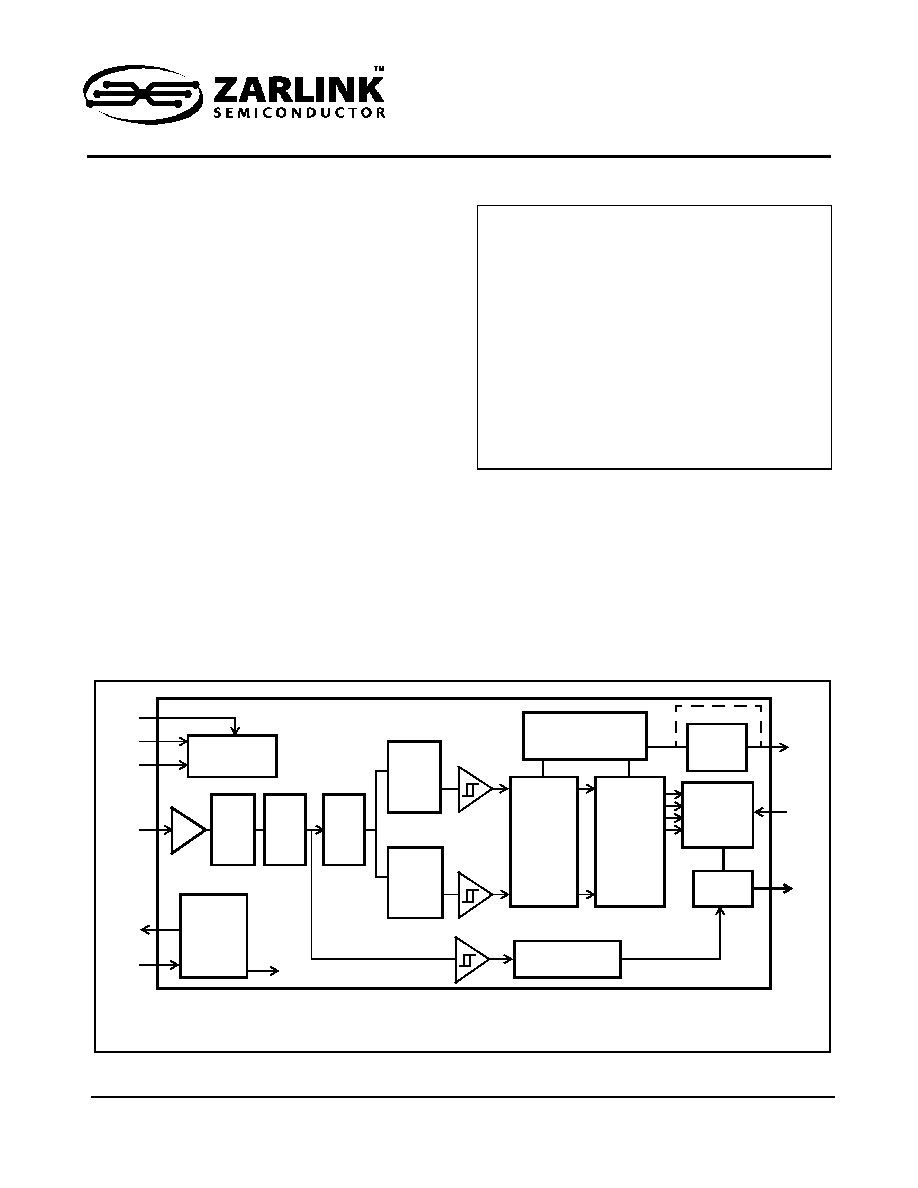
Figure 1 - Functional Block Diagram
PWDN
VDD
VSS
INPUT
OSC2
OSC1
(CLK)
MT3170B/71B and MT337xB only.
MT3270B/71B and MT337xB only.
Voltage
Bias Circuit
AGC
Anti-
alias
Filter
High
Group
Filter
Low
Group
Filter
Steering
Circuit
Digital
Detector
Algorithm
Code
Converter
and
Latch
Digital
Guard
Time
Parallel to
Serial
Converter
& Latch
Mux
Energy
Detection
Oscillator
and
Clock
Circuit
To All Chip Clocks
Dial
Tone
Filter
ESt
DStD
ACK
SD
or
MT3x71B only.
MT3170B/71B, MT3270B/71B, MT3370B/71B
Data Sheet
2
Zarlink Semiconductor Inc.
Description
The MT3x7xB is a family of high performance DTMF receivers which decode all 16 tone pairs into a 4-bit binary
code. These devices incorporate an AGC for wide dynamic range and are suitable for end-to-end signalling. The
MT3x70B provides an early steering (ESt) logic output to indicate the detection of a DTMF signal and requires
external software guard time to validate the DTMF digit. The MT3x71B, with preset internal guard times, uses a
delay steering (DStD) logic output to indicate the detection of a valid DTMF digit. The 4-bit DTMF binary digit can be
clocked out synchronously at the serial data (SD) output. The SD pin is multiplexed with call progress detector
output. In the presence of supervisory tones, the call progress detector circuit indicates the cadence (i.e., envelope)
of the tone burst. The cadence information can then be processed by an external microcontroller to identify specific
call progress signals. The MT327xB and MT337xB can be used with a crystal or a ceramic resonator without
additional components. A power-down option is provided for the MT317xB and MT337xB.
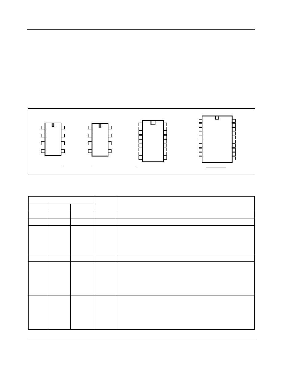
Figure 2 - Pin Connections
Pin Description
Pin #
Name
Description
337xB
327xB
317xB
2
1
1
INPUT
DTMF/CP Input. Input signal must be AC coupled via capacitor.
4
2
-
OSC2
Oscillator Output.
6
3
3
OSC1
(CLK)
Oscillator/Clock Input. This pin can either be driven by:
1)
an external digital clock with defined input logic levels. OSC2
should be left open.
2)
connecting a crystal or ceramic resonator between OSC1 and
OSC2 pins.
9
4
4
V
SS
Ground. (0V)
11
5
5
SD
Serial Data/Call Progress Output. This pin serves the dual function
of being the serial data output when clock pulses are applied after
validation of DTMF signal, and also indicates the cadence of call
progress input. As DTMF signal lies in the same frequency band as
call progress signal, this pin may toggle for DTMF input. The SD pin
is at logic low in powerdown state.
13
6
6
ACK
Acknowledge Pulse Input. After ESt or DStD is high, applying a
sequence of four pulses on this pin will then shift out four bits on the
SD pin, representing the decoded DTMF digit. The rising edge of the
first clock is used to latch the 4-bit data prior to shifting. This pin is
pulled down internally. The idle state of the ACK signal should be
low.
10
18
17
16
15
14
13
12
11
VDD
NC
NC
ESt/DStD
NC
ACK
NC
SD
NC
1
2
3
4
5
6
7
8
9
NC
INPUT
PWDN
OSC2
NC
OSC1
NC
NC
VSS
INPUT
PWDN
CLK
VSS
VDD
ACK
SD
INPUT
OSC2
OSC1
VSS
VDD
ESt/
ACK
SD
MT3170B/71B
MT3270B/71B
MT3370B/71B
8 PIN PLASTIC DIP
18 PIN PLASTIC SOIC
1
2
3
4
8
7
6
5
1
2
3
4
8
7
6
5
1
2
3
4
5
6
7
8
9
10
11
12
20
19
18
17
16
15
14
13
NC
NC
INPUT
PWDN
NC
NC
OSC1
OSC2
VSS
20 PIN SSOP
NC
VDD
NC
NC
ACK
SD
NC
NC
ESt/DStD
DStD
ESt/
DStD
MT3370B/71B
NC
NC

MT3170B/71B, MT3270B/71B, MT3370B/71B
Data Sheet
3
Zarlink Semiconductor Inc.
Functional Description
The MT3x7xBs are high performance and low power consumption DTMF receivers. These devices provide wide
dynamic range DTMF detection and a serial decoded data output. These devices also incorporate an energy
detection circuit. An input voiceband signal is applied to the devices via a series decoupling capacitor. Following the
unity gain buffering, the signal enters the AGC circuit followed by an anti-aliasing filter. The bandlimited output is
routed to a dial tone filter stage and to the input of the energy detection circuit. A bandsplit filter is then used to
separate the input DTMF signal into high and low group tones. The high group and low group tones are then
verified and decoded by the internal frequency counting and DTMF detection circuitry. Following the detection
stage, the valid DTMF digit is translated to a 4-bit binary code (via an internal look-up ROM). Data bits can then be
shifted out serially by applying external clock pulses.
Automatic Gain Control (AGC) Circuit
As the device operates on a single power supply, the input signal is biased internally at approximately VDD/2. With
large input signal amplitude (between 0 and approximately -30 dBm for each tone of the composite signal), the
15
7
7
ESt
(MT3x70B)
DStD
(MT3x71B)
Early Steering Output. A logic high on ESt indicates that a DTMF
signal is present. ESt is at logic low in powerdown state.
Delayed Steering Output. A logic high on DStD indicates that a
valid DTMF digit has been detected. DStD is at logic low in
powerdown state.
18
8
8
V
DD
Positive Power Supply (5 V Typ.) Performance of the device can
be optimized by minimizing noise on the supply rails. Decoupling
capacitors across V
DD
and V
SS
are therefore recommended.
1,5,7,8,
10, 12,
14,16,
17
-
-
NC
No Connection. Pin is unconnected internally.
3
-
2
PWDN Power Down Input. A logic high on this pin will power down the
device to reduce power consumption. This pin is pulled down
internally and can be left open if not used. ACK pin should be at logic
'0' to power down device.
Summary of MT3x70/71B Product Family
Device
Type
8 Pin
18 Pin
20 Pin
PWDN
2 Pin
OSC
Ext
CLK
ESt
DStD
MT3170B
MT3171B
MT3270B
MT3271B
MT3370B
MT3371B
Pin Description
Pin #
Name
Description
337xB
327xB
317xB

MT3170B/71B, MT3270B/71B, MT3370B/71B
Data Sheet
4
Zarlink Semiconductor Inc.
AGC is activated to prevent the input signal from being clipped. At low input level, the AGC remains inactive and the
input signal is passed directly to the hardware DTMF detection algorithm and to the energy detection circuit.
Filter and Decoder Section
The signal entering the DTMF detection circuitry is filtered by a notch filter at 350 and 440 Hz for dial tone rejection.
The composite dual-tone signal is further split into its individual high and low frequency components by two 6
th
order switched capacitor bandpass filters. The high group and low group tones are then smoothed by separate
output filters and squared by high gain limiting comparators. The resulting squarewave signals are applied to a
digital detection circuit where an averaging algorithm is employed to determine the valid DTMF signal. For
MT3x70B, upon recognition of a valid frequency from each tone group, the early steering (ESt) output will go high,
indicating that a DTMF tone has been detected. Any subsequent loss of DTMF signal condition will cause the ESt
pin to go low. For MT3x71B, an internal delayed steering counter validates the early steering signal after a
predetermined guard time which requires no external components. The delayed steering (DStD) will go high only
when the validation period has elapsed. Once the DStD output is high, the subsequent loss of early steering signal
due to DTMF signal dropout will activate the internal counter for a validation of tone absent guard time. The DStD
output will go low only after this validation period.
Energy Detection
The output signal from the AGC circuit is also applied to the energy detection circuit. The detection circuit consists
of a threshold comparator and an active integrator. When the signal level is above the threshold of the internal
comparator (-35dBm), the energy detector produces an energy present indication on the SD output. The integrator
ensures the SD output will remain at high even though the input signal is changing. When the input signal is
removed, the SD output will go low following the integrator decay time. Short decay time enables the signal
envelope (or cadence) to be generated at the SD output. An external microcontroller can monitor this output for
specific call progress signals. Since presence of speech and DTMF signals (above the threshold limit) can cause
the SD output to toggle, both ESt (DStD) and SD outputs should be monitored to ensure correct signal identification.
As the energy detector is multiplexed with the digital serial data output at the SD pin, the detector output is selected
at all times except during the time between the rising edge of the first pulse and the falling edge of the fourth pulse
applied at the ACK pin.
Serial Data (SD) Output
When a valid DTMF signal burst is present, ESt or DStD will go high. The application of four clock pulses on the
ACK pin will provide a 4-bit serial binary code representing the decoded DTMF digit on the SD pin output. The rising
edge of the first pulse applied on the ACK pin latches and shifts the least significant bit of the decoded digit on the
SD pin. The next three pulses on ACK pin will shift the remaining latched bits in a serial format (see Figure 5). If less
than four pulses are applied to the ACK pin, new data cannot be latched even though ESt/DStD can be valid. Clock
pulses should be applied to clock out any remaining data bits to resume normal operation. Any transitions in excess
of four pulses will be ignored until the next rising edge of the ESt/DStD. ACK should idle at logic low. The 4-bit
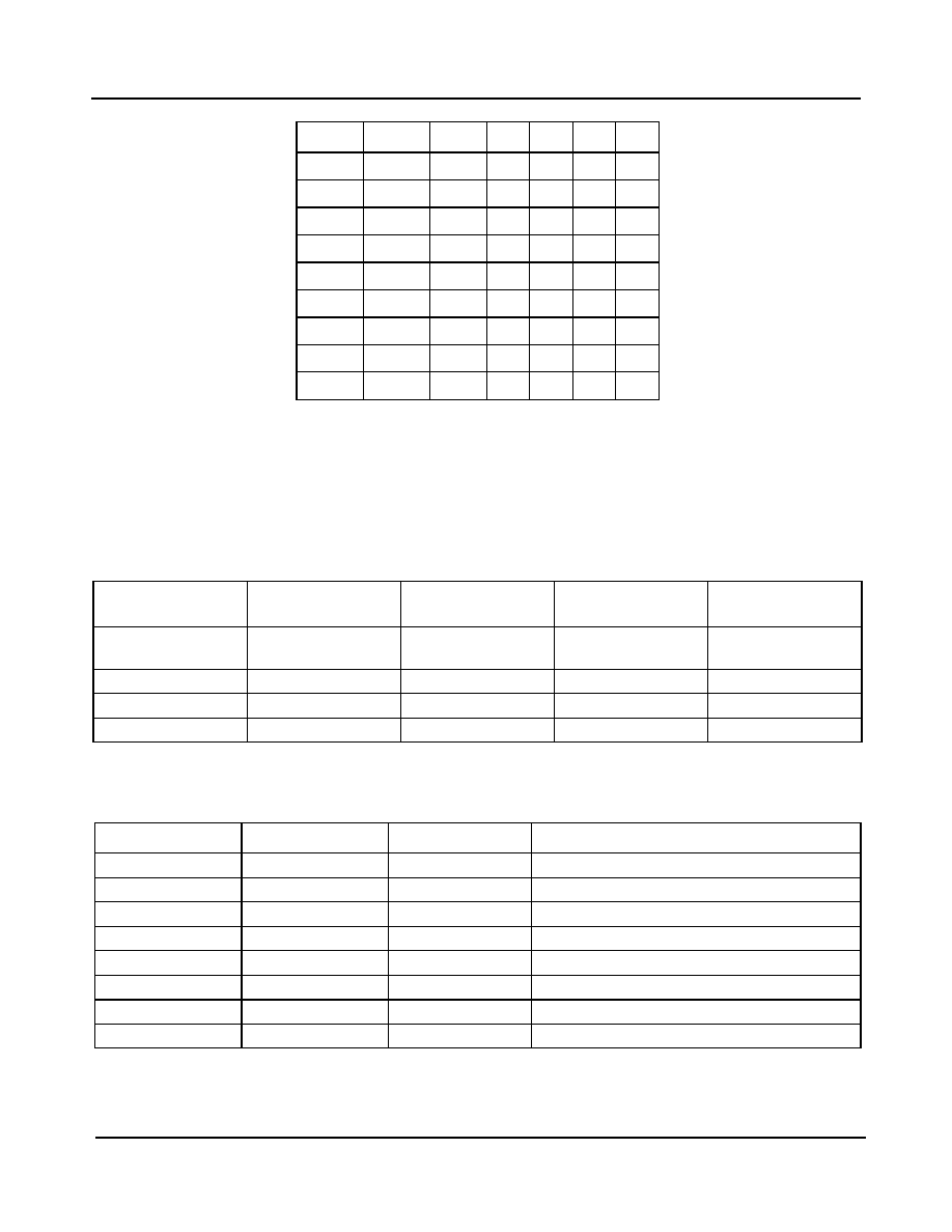
binary representing all 16 standard DTMF digits are shown in Table 1.
F
LOW
F
HIGH
DIGIT
b
3
b
2
b
1
b
0
697
1209
1
0
0
0
1
697
1336
2
0
0
1
0
697
1477
3
0
0
1
1
770
1209
4
0
1
0
0
770
1336
5
0
1
0
1
770
1477
6
0
1
1
0
852
1209
7
0
1
1
1
MT3170B/71B, MT3270B/71B, MT3370B/71B
Data Sheet
5
Zarlink Semiconductor Inc.
0= LOGIC LOW, 1= LOGIC HIGH
Table 1 - Serial Decode Bit Table
Note:
b0=LSB of decoded DTMF digit and shifted out first.
Powerdown Mode (MT317xB/337xB)
The MT317xB/337xB devices offer a powerdown function to preserve power consumption when the device is not in
use. A logic high can be applied at the PWDN pin to place the device in powerdown mode. The ACK pin should be
kept at logic low to avoid undefined ESt/DStD and SD outputs (see Table 2).
Table 2 - Powerdown Mode
+
=enters powerdown mode on the rising edge.
Table 3 - Call Progress Tones
852
1336
8
1
0
0
0
852
1477
9
1
0
0
1
941
1336
0
1
0
1
0
941
1209
*
1
0
1
1
941
1477
#
1
1
0
0
697
1633
A
1
1
0
1
770
1633
B
1
1
1
0
852
1633
C
1
1
1
1
941
1633
D
0
0
0
0
ACK (input)
PWDN (input)
ESt/DStD (output)
SD (output)
MT317xB/337xB
status
low
low
Refer to Fig. 4 for
timing waveforms
Refer to Fig. 4 for
timing waveforms
normal operation
low
high
+
low
low
powerdown mode
high
low
low
undefined
undefined
high
high
undefined
undefined
undefined
Frequency 1 (Hz)
Frequency 2 (Hz)
On/Off
Description
350
440
continuous
North American Dial Tones
425
---
continuous
European Dial Tones
400
---
continuous
Far East Dial Tones
480
620
0.5s/0.5s
North American Line Busy
440
---
0.5s/0.5s
Japanese Line Busy
480
620
0.25s/0.25s
North American Reorder Tones
440
480
2.0s/4.0s
North American Audible Ringing
480
620
0.25s/0.25s
North American Reorder Tones
F
LOW
F
HIGH
DIGIT
b
3
b
2
b
1
b
0