Document Outline
- Features
- Applications
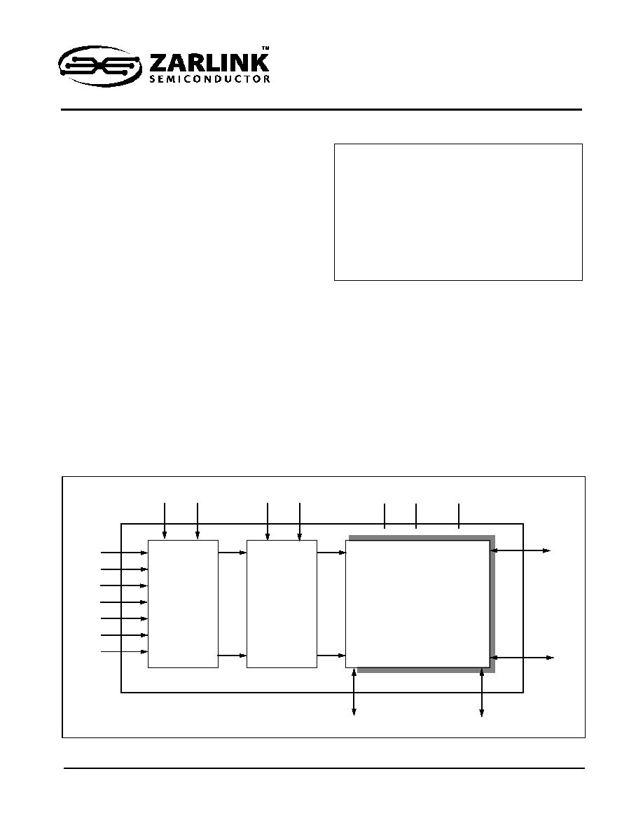
- Figure 1 - Functional Block Diagram
- Description
- Figure 2 - Pin Connections
- Pin Description�
- Functional Description
- Address Decode
- Absolute Maximum Ratings*- Voltages are with respect to VEE unless otherwise stated.
- Recommended Operating Conditions - Voltages are with respect to VEE unless otherwise stated.
- DC Electrical CharacteristicsÅ- Voltages are with respect to VEE = VSS = 0�V, VDD =12�V unless ot...
- DC Electrical Characteristics- Switch Resistance - VDC is the external DC offset applied at the a...
- AC Electrical CharacteristicsÅ - Crosspoint Performance-Voltages are with respect to VDD= 5�V, VS...
- AC Electrical CharacteristicsÅ - Control and I/O Timings- Voltages are with respect to VDD = 5�V,...
- Figure 3 - Control Memory Timing Diagram
- Table 1 - Address Decode Truth Table
1
Zarlink Semiconductor Inc.
Zarlink, ZL and the Zarlink Semiconductor logo are trademarks of Zarlink Semiconductor Inc.
Copyright 1997-2005, Zarlink Semiconductor Inc. All Rights Reserved.
Features
∑ Internal control latches and address decoder
∑ Short set-up and hold times
∑ Wide operating voltage: 4.5 V to 13.2 V
∑ 12Vpp analog signal capability
∑ R
ON
65
max. @ V
DD
= 12 V, 25
∞C
∑
R
ON
10 @ V
DD
= 12 V, 25
∞C
∑ Full CMOS switch for low distortion
∑ Minimum feedthrough and crosstalk
∑ Separate analog and digital reference supplies
∑ Low power consumption ISO-CMOS technology
Applications
∑ Key systems
∑ PBX systems
∑ Mobile radio
∑ Test equipment/instrumentation
∑ Analog/digital multiplexers
∑ Audio/Video switching
Description
The Zarlink MT8816 is fabricated in Zarlink's ISO-
CMOS technology providing low power dissipation and
high reliability. The device contains a 8 x 16 array of
crosspoint switches along with a 7 to 128 line decoder
and latch circuits. Any one of the 128 switches can be
addressed by selecting the appropriate seven address
bits. The selected switch can be turned on or off by
applying a logical one or zero to the DATA input. V
SS
is
the ground reference of the digital inputs. The range of
the analog signal is from V
DD
to V
EE
. Chip Select (CS)
allows the crosspoint array to be cascaded for matrix
expansion.
February 2005
Ordering Information
MT8816AE
40 Pin PDIP
Tubes
MT8816AP
44 Pin PLCC
Tubes
MT8816APR
44 Pin PLCC
Tape & Reel
MT8816AP1
44 Pin PLCC*
Tubes
MT8816APR1 44 Pin PLCC*
Tape & Reel
MT8816AE1
40 Pin PDIP*
Tubes
* Pb Free Matte Tin
-40
∞C to +85∞C
MT8816
ISO-CMOS
8 x 16 Analog Switch Array
Data Sheet
Figure 1 - Functional Block Diagram
7 to 128
Decoder
Latches
8 x 16
Switch
Array
CS
STROBE
DATA RESET
VDD
VEE
VSS
Xi I/O
(i=0-15)
Yi I/O (i=0-7)
1
1
128
128
∑ ∑ ∑ ∑ ∑ ∑ ∑ ∑ ∑ ∑ ∑ ∑ ∑ ∑ ∑ ∑ ∑ ∑ ∑
∑ ∑
∑ ∑ ∑ ∑
∑ ∑ ∑
∑ ∑ ∑ ∑
∑ ∑ ∑
AX0
AX1
AY0
AY1
AY2
AX2
AX3

MT8816
Data Sheet
2
Zarlink Semiconductor Inc.
Figure 2 - Pin Connections
Pin Description
Pin #
Name
Description
PDIP
PLCC
1
1
Y3
Y3 Analog (Input/Output): this is connected to the Y3 column of the switch array.
2
2
AY2
Y2 Address Line (Input).
3
3
RESET Master RESET (Input): this is used to turn off all switches regardless of the
condition of CS. Active High.
4,5
4,5
AX3,AX0 X3 and X0 Address Lines (Inputs).
6,7
7,8
X14, X15 X14 and X15 Analog (Inputs/Outputs): these are connected to the X14 and X15
rows of the switch array.
8-13
9-14
X6-X11 X6-X11 Analog (Inputs/Outputs): these are connected to the X6-X11 rows of the
switch array.
14
6,15,16
NC
No Connection
15
17
Y7
Y7 Analog (Input/Output): this is connected to the Y7 column of the switch array.
16
18
V
SS
Digital Ground Reference.
17
19
Y6
Y6 Analog (Input/Output): this is connected to the Y6 column of the switch array.
18
20
STROBE STROBE (Input): enables function selected by address and data. Address must
be stable before STROBE goes high and DATA must be stable on the falling edge
of the STROBE. Active High.
19
21
Y5
Y5 Analog (Input/Output): this is connected to the Y5 column of the switch array.
20
22
V
EE
Negative Power Supply.
21
23
Y4
Y4 Analog (Input/Output): this is connected to the Y4 column of the switch array.
22, 23
24,25
AX1,AX2 X1 and X2 Address Lines (Inputs).
40 PIN PLASTIC DIP
44 PIN PLCC
2
3
4
5
6
7
8
9
10
11
12
13
14
15
16
17
18
19
20
1
40
39
38
37
36
35
34
33
32
31
30
29
28
27
26
25
24
23
22
21
AY2
RESET
AX3
AX0
X14
X15
X6
X7
X8
X9
X10
X11
NC
Y7
VSS
Y6
STROBE
Y5
VEE
Y3
Y2
DATA
Y1
CS
Y0
NC
X0
X1
X2
X3
X4
X5
X12
X13
AY1
AY0
AX2
AX1
Y4
VDD
X14
X15
X6
X7
X8
X9
X10
X11
NC
NC
Y7
VSS
Y6
STROBE
Y5
VEE
AX1
AX2
AY0
AY1
NC
Y4
1
6 5 4 3 2
44 43 42 41 40
7
8
9
10
11
12
13
14
15
16
39
38
37
36
35
34
33
32
31
30
23
18 19 20 21 22
24 25 26 27 28
17
29
Y0
NC
X0
X1
X2
X3
X4
X5
X12
X13
NC
CS
Y1
DA
T
A
Y2
VD
D
Y3
AY
2
RE
SET
AX
3
AX
0
NC
MT8816
Data Sheet
3
Zarlink Semiconductor Inc.
24, 25
26,27
AY0,AY1 Y0 and Y1 Address Lines (Inputs).
26, 27
30,31
X13, X12 X13 and X12 Analog (Inputs/Outputs): these are connected to the X13 and X12
rows of the switch array.
28 - 33
32-37
X5-X0
X5-X0 Analog (Inputs/Outputs): these are connected to the X5-X0 rows of the
switch array.
34
28,29,
38
NC
No Connection.
35
39
Y0
Y0 Analog (Input/Output): this is connected to the Y0 column of the switch array.
36
40
CS
Chip Select (Input): this is used to select the device. Active High.
37
41
Y1
Y1 Analog (Input/Output): this is connected to the Y1 column of the switch array.
38
42
DATA
DATA (Input): a logic high input will turn on the selected switch and a logic low will
turn off the selected switch. Active High.
39
43
Y2
Y2 Analog (Input/Output): this is connected to the Y2 column of the switch array.
40
44
V
DD
Positive Power Supply.
Pin Description (continued)
Pin #
Name
Description
PDIP
PLCC

MT8816
Data Sheet
4
Zarlink Semiconductor Inc.
Functional Description
The MT8816 is an analog switch matrix with an array size of 8 x 16. The switch array is arranged such that there
are 8 columns by 16 rows. The columns are referred to as the Y inputs/outputs and the rows are the X
inputs/outputs. The crosspoint analog switch array will interconnect any X I/O with any Y I/O when turned on and
provide a high degree of isolation when turned off. The control memory consists of a 128 bit write only RAM in
which the bits are selected by the address inputs (AY0-AY2, AX0-AX3). Data is presented to the memory on the
DATA input. Data is asynchronously written into memory whenever both the CS (Chip Select) and STROBE inputs
are high and are latched on the falling edge of STROBE. A logical "1" written into a memory cell turns the
corresponding crosspoint switch on and a logical "0" turns the crosspoint off. Only the crosspoint switches
corresponding to the addressed memory location are altered when data is written into memory. The remaining
switches retain their previous states. Any combination of X and Y inputs/outputs can be interconnected by
establishing appropriate patterns in the control memory. A logical "1" on the RESET input will asynchronously return
all memory locations to logical "0" turning off all crosspoint switches regardless of whether CS is high or low.
Two voltage reference pins (V
SS
and V
EE
) are provided for the MT8816 to enable switching of negative analog
signals. The range for digital signals is from V
DD
to V
SS
while the range for analog signals is from V
DD
to V
EE
. V
SS
and V
EE
pins can be tied together if a single voltage reference is needed.
Address Decode
The seven address inputs along with the STROBE and CS (Chip Select) are logically ANDed to form an enable
signal for the resettable transparent latches. The DATA input is buffered and is used as the input to all latches. To
write to a location, RESET must be low and CS must go high while the address and data are set up. Then the
STROBE input is set high and then low causing the data to be latched. The data can be changed while STROBE is
high, however, the corresponding switch will turn on and off in accordance with the DATA input. DATA must be
stable on the falling edge of STROBE in order for correct data to be written to the latch.
MT8816
Data Sheet
5
Zarlink Semiconductor Inc.
* Exceeding these values may cause permanent damage. Functional operation under these conditions is not implied.
DC Electrical Characteristics are over recommended temperature range.
Typical figures are at 25
∞
C and are for design aid only; not guaranteed and not subject to production testing.
Absolute Maximum Ratings*
- Voltages are with respect to V
EE
unless otherwise stated.
Parameter
Symbol
Min.
Max.
Units
1
Supply Voltage
V
DD
V
SS
-0.3
-0.3
16.0
V
DD
+0.3
V
V
2
Analog Input Voltage
V
INA
-0.3
V
DD
+0.3
V
3
Digital Input Voltage
V
IN
V
SS
-0.3
V
DD
+0.3
V
4
Current on any I/O Pin
I
±15
mA
5
Storage Temperature
T
S
-65
+150
∞C
6
Package Power Dissipation
PLASTIC DIP
P
D
0.6
W
Recommended Operating Conditions
- Voltages are with respect to V
EE
unless otherwise stated.
Characteristics
Sym.
Min.
Typ.
Max.
Units
Test Conditions
1
Operating Temperature
T
O
-40
25
85
∞C
2
Supply Voltage
V
DD
V
SS
4.5
V
EE
13.2
V
DD
-4.5
V
V
3
Analog Input Voltage
V
INA
V
EE
V
DD
V
4
Digital Input Voltage
V
IN
V
SS
V
DD
V
DC Electrical Characteristics
-
Voltages are with respect to V
EE
= V
SS
= 0 V, V
DD
=12 V unless otherwise stated.
Characteristics
Sym.
Min.
Typ.
Max.
Units
Test Conditions
1
Quiescent Supply Current
I
DD
1
100
µA
All digital inputs at V
IN
=V
SS
or
V
DD
0.4
1.5
mA
All digital inputs at V
IN
=2.4V +
V
SS
; V
SS
=7.0 V
5
15
mA
All digital inputs at V
IN
=3.4 V
2
Off-state Leakage Current
(See G.9 in Appendix)
I
OFF
±1
±500
nA
IV
Xi
- V
Yj
I = V
DD
- V
EE
See Appendix, Fig. A.1
3
Input Logic "0" level
V
IL
0.8+V
S
S
V
V
SS
=7.5V; V
EE
=0 V
4
Input Logic "1" level
V
IH
2.0+V
SS
V
V
SS
=6.5V; V
EE
=0 V
5
Input Logic "1" level
V
IH
3.3
V
6
Input Leakage (digital pins)
I
LEAK
0.1
10
µA
All digital inputs at V
IN
= V
SS
or V
DD