
Obsolescence Notice
This product is obsolete.
This information is available for your
convenience only.
For more information on
Zarlink's obsolete products and
replacement product lists, please visit
http://products.zarlink.com/obsolete_products/

SEMICMF.019
1
MT88E41
Extended Voltage Calling Number
Identification Circuit (ECNIC)
Data Sheet
Features
�
1200 baud BELL 202 and CCITT V.23 Frequency
Shift Keying (FSK) demodulation
�
Compatible with Bellcore GR-30-CORE and SR-
TSV-002476
�
High input sensitivity: -36dBm minimum FSK
Detection Level
�
Simple serial 3-wire data interface eliminating the
need for a UART
�
Power down mode
�
Internal gain adjustable amplifier
�
Carrier detect status output
�
Uses 3.579545 MHz crystal
�
2.7 - 5.5V operation
�
Low power CMOS technology
Applications
�
Calling Number Delivery (CND), Calling Name
Delivery (CNAM) and Calling Identity on Call
Waiting (CIDCW) features of Bellcore CLASS
SM
service
�
Feature phones
�
Phone sets, adjunct boxes
�
FAX machines
�
Telephone answering machines
�
Database query systems
�
Battery powered applications
Description
The MT88E41 Extended Voltage Calling Number
Identification Circuit (ECNIC) is a CMOS integrated
circuit providing an interface to various calling line
information delivery services that utilize 1200 baud
BELL 202 or CCITT V.23 FSK voiceband data
transmission schemes. The ECNIC receives and
demodulates the signal and outputs data into a simple
3-wire serial interface.
Typically, the FSK modulated data containing
information on the calling line is sent before alerting the
called party or during the silent interval between the first
and second ring using either CCITT V.23
recommendations or Bell 202 specifications.
The ECNIC accepts and demodulates both CCITT V.23
and BELL 202 signals. Along with serial data and clock,
the ECNIC provides a data ready signal to indicate the
reception of every 8-bit character sent from the Central
DS5717
Issue 3
February 1998
Ordering Information
MT88E41AE
16 Pin Plastic DIP
MT88E41AS
16 Pin SOIC
MT88E41AN
20 Pin SSOP
-40
�
C to +85
�
C
Figure 1 - Functional Block Diagram
CLASS
SM
is a service mark of Bellcore
GS
IN-
IN+
CAP
VRef
DATA
DR
DCLK
CD
PWDN
OSC1 OSC2
VSS
VDD IC1
IC2
Receive
Bandpass
Filter
Bias
Generator
FSK
Demodulator
Data and Timing
Carrier
Detector
Clock
Generator
Recovery
to other
circuits
-
+
CMOS

MT88E41
Data Sheet
SEMICMF.019
2
Office. The received data can be processed externally by a microcontroller, stored in memory, or displayed as
is, depending on the application.
Figure 2 - Pin Connections
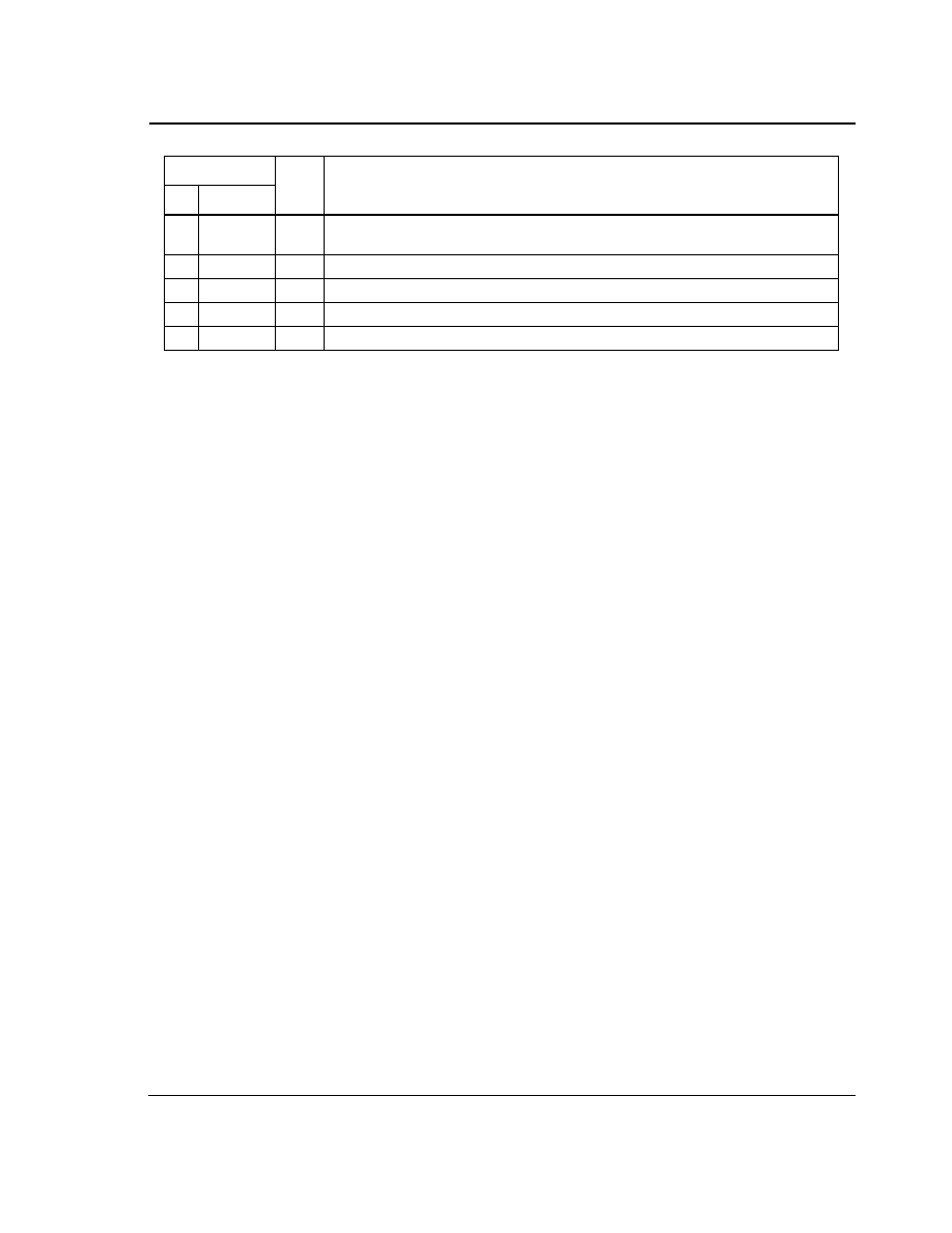
Pin Description Table
Pin
#
Name
Description
16
20
1
1
IN+
Non-inverting Op-Amp (Input).
2
2
IN-
Inverting Op-Amp (Input).
3
3
GS
Gain Select (Output). Gives access to op-amp output for connection of feedback
resistor.
4
4
V
Ref
Voltage Reference (Output). Nominally V
DD/2
. This is used to bias the op-amp
inputs.
5
5
CAP Capacitor. Connect a 0.1
�
F capacitor to V
SS
.
6
7
OSC1 Oscillator (Input). Crystal connection. This pin can be driven directly from an
external clocking source.
7
9
OSC2 Oscillator (Output). Crystal connection. When OSC1 is driven by an external
clock, this pin should be left open.
8
10
V
SS
Power supply ground.
9
11
DCLK Data Clock (Output). Outputs a clock burst of 8 low going pulses at 1202.8Hz
(3.5795MHz divided by 2976). Every clock burst is initiated by the DATA stop bit
start bit sequence. When the input DATA is 1202.8 baud, the positive edge of each
DCLK pulse coincides with the middle of the data bits output at the DATA pin. No
DCLK pulses are generated during the start or stop bits. Typically, DCLK is used to
clock the eight data bits from the 10 bit data word into a serial-to-parallel converter.
10
12
DATA Data (Output). Serial data output corresponding to the FSK input and switching at
the input baud rate. Mark frequency at the input corresponds to a logic high, while
space frequency corresponds to a logic low at the DATA output. With no FSK
input, DATA is at logic high. This output stays high until CD
has become active.
11
13
DR
Data Ready (Open Drain Output). This output goes low after the last DCLK pulse
of each word. This can be used to identify the data (8-bit word) boundary on the
serial output stream. Typically, DR is used to latch the eight data bits from the
serial-to-parallel converter into a microcontroller.
12
14
CD
Carrier Detect (Open Drain Output). A logic low indicates that a carrier has been
present for a specified time on the line. A time hysteresis is provided to allow for
momentary discontinuity of carrier.
1
2
3
4
5
6
7
8
16
15
14
13
12
11
10
9
IN+
IN-
GS
VRef
CAP
OSC1
OSC2
VSS
VDD
IC2
IC1
PWDN
CD
DR
DATA
DCLK
16 PIN PLASTIC DIP/SOIC
1
2
3
4
5
6
7
8
9
10
11
12
20
19
18
17
16
15
14
13
IN+
IN-
GS
VRef
CAP
NC
OSC1
NC
OSC2
VSS
20 PIN SSOP
VDD
IC2
NC
NC
PWDN
CD
DR
DATA
DCLK
IC1
Data Sheet
MT88E41
3
SEMICMF.019
13
15
PWDN Power Down (Input). Active high, Schmitt Trigger input. Powers down the device
including the input op-amp and the oscillator.
14
16
IC1
Internal Connection 1. Connect to V
SS
.
15
19
IC2
Internal Connection 2. Internally connected, leave open circuit.
16
20
V
DD
Positive power supply voltage.
6, 8, 17, 18
NC
No Connection.
Pin Description Table (continued)
Pin
#
Name
Description
16
20

MT88E41
Data Sheet
SEMICMF.019
4
1.0
Functional Description
The MT88E41 Extended Voltage Calling Number Identification Circuit (ECNIC) is a device compatible with the
Bellcore proposal (GR-30-CORE) on generic requirements for transmitting asynchronous voiceband data to
Customer Premises Equipment (CPE) from a serving Stored Program Controlled Switching System (SPCS) or a
Central Office (CO). This data transmission technique is applicable in a variety of services like Calling Number
Delivery (CND), Calling Name Delivery (CNAM) or Calling Identity Delivery on Call Waiting (CIDCW) as specified in
Custom Local Area Signalling Service (CLASS
SM
) calling information delivery features by Bellcore.
With CND, CNAM and CIDCW service, the called subscriber has the capability to display or to store the information
on the calling party which is sent by the CO and received by the ECNIC.
In the CND service, information about a calling party is embedded in the silent interval between the first and second
ring. During this period, the ECNIC receives and demodulates the 1200 baud FSK signal (compatible with Bell-202
specification) and outputs data into a 3-wire serial interface.
In the CIDCW service, information about a second calling party is sent to the subscriber, (while the subscriber is
engaged in another call). During this period, the ECNIC receives and demodulates the FSK signal as in the CND
case.
The ECNIC is designed to provide the data transmission interface required for the above service at the called
subscriber location either in the on-hook case as in CND, or the off-hook case, as in CIDCW. The functional
block diagram of the ECNIC is shown in Figure 1. Note however, for CIDCW applications, a separate CAS (CPE
Alerting Signal) detector is required.
Figure 3 - Differential Input Configuration
C1
R1
C2
R4
R3
R2
R5
IN+
IN-
GS
V
Ref
MT88E41
DIFFERENTIAL INPUT AMPLIFIER
C1 = C2 = 10 nF
R1 = R4 = R5 = 100 k
R2 = 60k
, R3 = 37.5 k
R3 = (R2R5) / (R2 + R5)
VOLTAGE GAIN
(A
V
diff) = R5/R1
INPUT IMPEDANCE
(Z
IN
diff) = 2
R1
2
+ (1/
C)
2