 | –≠–ª–µ–∫—Ç—Ä–æ–Ω–Ω—ã–π –∫–æ–º–ø–æ–Ω–µ–Ω—Ç: MT88E43AS | –°–∫–∞—á–∞—Ç—å:  PDF PDF  ZIP ZIP |
5-53
Features
∑
Compatible with:
∑
British Telecom (BT) SIN227 & SIN242
∑
U.K.'s Cable Communications Association
(CCA) specification TW/P&E/312
∑
Bellcore GR-30-CORE (formerly known as
TR-NWT-000030) & SR-TSV-002476
∑
Bellcore "CPE Alerting Signal (CAS)" and BT
"Idle State Tone Alert Signal" detection
∑
Ring and line reversal detection
∑
1200 baud Bell 202 and CCITT V.23 Frequency
Shift Keying (FSK) demodulation
∑
3 or 5V
±
10% supply voltage
∑
High input sensitivity (-40dBV Tone and FSK
Detection)
∑
Selectable 3-wire data interface
(microcontroller or MT88E43 controlled)
∑
Low power CMOS with powerdown mode
∑
Input gain adjustable amplifier
∑
Carrier detect status output
∑
Uses 3.58 MHz crystal
Applications
∑
BT Calling Line Identity Presentation (CLIP),
CCA CLIP, and Bellcore Calling Identity
Delivery (CID) systems
∑
Feature phones, including Analog Display
Services Interface (ADSI) phones
∑
Phone set adjunct boxes
∑
FAX and answering machines
∑
Database query and Computer Telephony
Integration (CTI) systems
Description
The MT88E43 Calling Number Identification Circuit 2
(ECNIC2) is a low power CMOS integrated circuit
intended for receiving physical layer signals
transmitted according to BT (British Telecom)
SIN227 & SIN242, the U.K.'s CCA (Cable
Communications Association) TW/P&E/312 and
Bellcore GR-30-CORE & SR-TSV-002476
specifications. The MT88E43 is suitable for
applications using a fixed voltage power source
between 3 and 5V
±
10%.
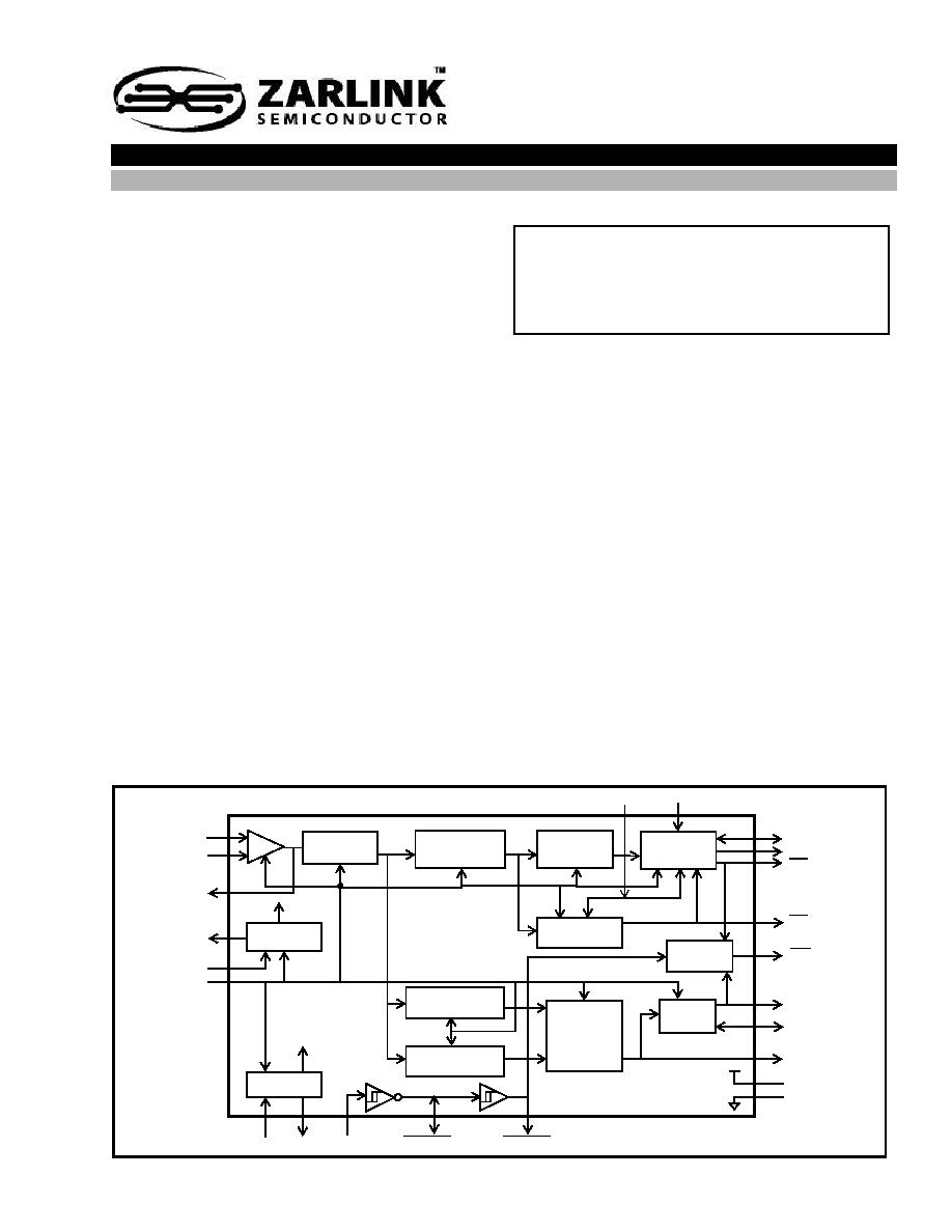
Figure 1- Functional Block Diagram
+
-
Anti-alias
Filter
FSK Bandpass
Filter
FSK
Demodulator
Data Timing
Recovery
Carrier
Detector
Alert Signal High
Tone Filter
Alert Signal Low
Tone Filter
Tone
Detection
Algorithm
Bias
Generator
Oscillator
Guard
Time
StD
St/GT
ESt
TRIGout
TRIGRC
TRIGin
DATA
DR
DCLK
MODE
FSKen
CD
CAP
OSCin OSCout
IN+
IN-
GS
VRef
INT
PWDN
VDD
VSS
To internal
To internal cct.
cct.
Interrupt
Generator
ISSUE 3
March 1997
Ordering Information
MT88E43AE
24 Pin Plastic DIP
(0.6 inch package only)
MT88E43AS
24 Pin SOIC
-40
∞
C to +85
∞
C
MT88E43
Extended Voltage Calling Number
Identification Circuit 2
CMOS

MT88E43
Data Sheet
5-54
Figure 2 - Pin Connections
Pin Description
Pin #
Name
Description
1
IN+
Non-inverting Input of the internal opamp.
2
IN-
Inverting Input of the internal opamp.
3
GS
Gain Select (Output) of internal opamp. The opamp's gain should be set according to the
nominal Vdd of the application using the information in Figure 10.
4
V
Ref
Reference Voltage (Output). Nominally V
DD
/2
. It is used to bias the input opamp.
5
CAP
Capacitor. A 0.1
µ
F decoupling capacitor should be connected across this pin and V
SS
.
6
TRIGin
Trigger Input. Schmitt trigger buffer input. Used for line reversal and ring detection.
7
TRIGRC
Trigger RC (Open Drain Output/Schmitt Input). Used to set the (RC) time interval from
TRIGin going low to TRIGout going high. An external resistor connected to V
DD
and capacitor
connected to V
SS
determine the duration of the (RC) time interval.
8
TRIGout
Trigger Out (CMOS Output). Schmitt trigger buffer output. Used to indicate detection of line
reversal and/or ringing.
9
MODE
3-wire interface: Mode Select (CMOS Input). When low, selects interface mode 0. When high,
selects interface mode 1. See pin 16 (DCLK) description to understand how MODE affects the
DCLK pin.
10
OSCin
Oscillator Input. A 3.579545MHz crystal should be connected between this pin and OSCout. It
may also be driven directly from an external clock source.
11
OSCout
Oscillator Output. A 3.579545MHz crystal should be connected between this pin and OSCin.
When OSCin is driven by an external clock, this pin should be left open.
12
V
SS
Power Supply Ground.
13
IC
Internal Connection. Must be connected to V
SS
for normal operation.
14
PWDN
Power Down (Schmitt Input). Active high. When high, the device consumes minimal power by
disabling all functionality except TRIGin, TRIGRC and TRIGout. Must be pulled low for device
operation.
15
FSKen
FSK Enable (CMOS Input). Must be high for FSK demodulation. This pin should be set low to
prevent the FSK demodulator from reacting to extraneous signals (such as speech, alert signal
and DTMF which are all in the same frequency band as FSK).
16
DCLK
3-wire Interface: Data Clock (CMOS Input/Output). In mode 0 (MODE pin low), this pin is an
output. In mode 1 (MODE pin high), this pin is an input.
17
DATA
3-wire Interface: Data (CMOS Output). In mode 0 data appears at the pin once demodulated.
In mode 1 data is shifted out on the rising edge of the microcontroller supplied DCLK.
VDD
St/GT
ESt
StD
INT
DR
DATA
DCLK
FSKen
PWDN
IC
CD
IN+
IN-
GS
VRef
CAP
TRIGin
TRIGRC
TRIGout
OSCin
OSCout
VSS
MODE
1
2
3
4
5
6
7
8
9
10
11
12
13
14
15
16
24
23
22
21
20
19
18
17

Data Sheet
MT88E43
5-55
18
DR
3-wire Interface: Data Ready (CMOS Output). Active low. In mode 0 this output goes low after
the last DCLK pulse of each data word. This identifies the 8-bit word boundary on the serial
output stream. Typically, DR is used to latch 8-bit words from a serial-to-parallel converter into a
microcontroller. In mode 1 this pin will signal the availability of data.
19
CD
Carrier Detect (CMOS Output). Active low. A logic low indicates the presence of in-band signal
at the output of the FSK bandpass filter.
20
INT
Interrupt (Open Drain Output). Active low. It is active when TRIGout or DR is low, or StD is
high. This output stays low until all three signals have become inactive.
21
StD
Dual Tone Alert Signal Delayed Steering Output (CMOS Output). When high, it indicates
that a guard time qualified alert signal has been detected.
22
ESt
Dual Tone Alert Signal Early Steering Output (CMOS Output). Alert signal detection output.
Used in conjunction with St/GT and external circuitry to implement the detect and non-detect
guard times.
23
St/GT
Dual Tone Alert Signal Steering Input/Guard Time (Analog Input/CMOS Output). A
voltage greater than V
TGt
(see figure 4) at the St/GT pin causes the device to indicate that a
dual tone has been detected by asserting StD high. A voltage less than V
TGt
frees the device to
accept a new dual tone.
24
V
DD
Positive Power Supply.
Pin Description
Pin #
Name
Description
The MT88E43 provides all the features and
functions offered by Zarlink's MT8841 (CNIC),
including 1200 baud Bell 202 and CCITT V.23 FSK
demodulation. The 3-wire serial data interface
provided by CNIC has been enhanced to operate in
two modes. In the CNIC compatible mode data
transfer is initiated by the device. A second mode
allows a microcontroller to extract 8-bit data words
from the device. Furthermore, the MT88E43 offers
Idle State Tone Alert Signal and line reversal
detection capability for BT's CLIP, ring burst
detection for the U.K.'s CCA's CLIP, and ring and
CAS detection for Bellcore's CID.
Functional Overview
The MT88E43, Extended Voltage Calling Number
Identification Circuit 2 (ECNIC2) is a device
compatible with BT, the U.K.'s CCA and Bellcore
specifications. As shown in Figure 1, the MT88E43
provides an FSK demodulator as well as a 3-wire
serial interface similar to that of it's predecessor, the
MT8841 (CNIC). The 3-wire interface has been
enhanced to provide two modes of operation - a
mode whereby data transfer is initiated by the device
and a mode whereby data transfer is initiated by an
external microcontroller.
In addition to supporting all the features and
functions of the MT8841, the MT88E43 also
provides line reversal detection, ring detection and
dual tone alert signal/CAS detection. These new
functions eliminate some external circuitry previously
required with the MT8841.
The MT88E43 is compatible with the caller identity
specifications of BT, the U.K.'s CCA, and Bellcore.
BT specifications SIN227 and SIN242 describe the
signalling mechanism between the network and the
Terminal Equipment (TE) for the Caller Display
Service (CDS). CDS provides Calling Line Identity
Presentation (CLIP), which delivers to an on hook
(idle state) TE the identity of an incoming caller
before the first ring.
An incoming CDS call is indicated by a polarity
reversal on the A and B wires (see Figure 3),
followed by an Idle State Tone Alert Signal. Caller ID
FSK information is then transmitted in CCITT V.23
format. MT88E43 can detect the line reversal, tone
alert signal, and demodulate the incoming CCITT
V.23 FSK signals.
The U.K.'s CCA specification TW/P&E/312 proposes
an alternate CDS TE interface. According to TW/
P&E/312, data is transmitted after a single burst of
ringing rather than before the first ringing cycle (as
specified in the BT standards). The Idle State Tone
Alert Signal is not required as it is replaced by a
single ring burst. MT88E43 has the capability to
detect the ring burst. It can also demodulate either

MT88E43
Data Sheet
5-56
Bell-202 or CCITT V.23 FSK data following the ring
burst. The U.K.'s CCA specifies that data can be
transmitted in either format.
Bellcore specification GR-30-CORE is the generic
requirement for transmitting asynchronous
voiceband data to Customer Premises Equipment
(CPE). Another Bellcore specification SR-TSV-
002476 describes the same requirements from the
CPE's perspective. The data transmission technique
specified in both documents is applicable in a variety
of services like Calling Number Delivery (CND),
Calling Name Delivery (CNAM) and Calling Identity
Delivery on Call Waiting (CIDCW) - services
promoted by Bellcore.
In CND/CNAM service, information about a calling
party is embedded in the silent interval between the
first and second ring burst. The MT88E43 detects
the first ring burst and can then be setup to receive
and demodulate the incoming Bell-202 FSK data.
The device will output the demodulated data onto a
3-wire serial interface.
In CIDCW service, information about an incoming
caller is sent to the subscriber, while he/she is
engaged in another call. A CPE Alerting Signal
(CAS) indicates the arrival of CIDCW information.
The MT88E43 can detect the alert signal and then be
setup to demodulate incoming FSK data containing
CIDCW information.
Functional Description
Detection of CLIP/CID Call Arrival Indicators
The circuit in Figure 3 illustrates the relationship
between the TRIGin, TRIGRC and TRIGout signals.
Typically, the three pin combination is used to detect
an event indicated by an increase of the TRIGin
voltage from V
SS
to above the Schmitt trigger high
going threshold V
T+
(see DC electrical
characteristics).
Figure 3 shows a circuit to detect any one of three
CLIP/CID call arrival indicators: line reversal, ring
burst and ringing.
1. Line Reversal Detection
Line reversal, or polarity reversal on the A and B
wires indicates the arrival of an incoming CDS call,
as specified in SIN227. When the event (line
reversal) occurs, TRIGin rises past the high going
Schmitt threshold V
T+
and TRIGout, which is
normally high, is pulled low. When the event is over,
TRIGin falls back to below the low going Schmitt
threshold V
T-
and TRIGout returns high. The
components R5 and C3 (see Figure 3) at TRIGRC
ensure a minimum TRIGout low interval.
In a TE designed for CLIP, the TRIGout high to low
transition may be used to interrupt or wake-up the
microcontroller. The controller can thus be put into
power-down mode to conserve power in a battery
operated TE.
Figure 3 - Circuit to Detect Line Reversal, Ring Burst and Ringing
Tip/A
C1=100nF
R1=499K
Ring/B
C2=100nF
R2=499K
MT88E43
TRIGout
To Microcontroller
R3=200K
R
4
=
3
0
1
K
R
5
=
1
5
0
K
C
3
=
2
2
0
n
F
TRIGRC
TRIGin
V
DD
V1
V2
V3
V4
max V
T+
= 0.68 V
DD
min VT+ = 0.48 V
DD
The application circuit must ensure that,
V
TRIGin
>max V
T+
where max V
T+
=3.74V @V
DD
=5.5V.
Tolerance to noise between A/B and V
SS
is:
max V
noise
= (min V
T+
)/0.30+0.7 =5.6Vrms @4.5V V
DD
where min V
T+
= 2.16V @V
DD
=4.5V.
Suggested R
5
C
3
component values:
R5 from 10K
to 500K
C3 from 47nF to 0.68
µ
F
An example is C3=220nF, R5=150K
; TRIGout low
from 21.6ms to 37.6ms after TRIGin Signal stops
triggering the circuit.
Notes:
To determine values for C3 and R5:
R5C3=-t / ln(1-V
TRIGRC
/V
DD
)

Data Sheet
MT88E43
5-57
2. Ring Burst Detection
CCA does not support the dual tone alert signal
(refer to Dual Tone Alert Signal Detection section).
Instead, CCA requires that the TE be able to detect a
single burst of ringing (duration 200-450ms) that
precedes CLIP FSK data. The ring burst may vary
from 30 to 75Vrms and is approximately 25Hz.
Again in a TE designed for CCA CLIP, the TRIGout
high to low transition may be used to interrupt or
wake-up the microcontroller. The controller can thus
be put into power-down mode to conserve power in a
battery operated TE.
3. Ring Detection
In Bellcore's CND/CNAM scheme, the CID FSK data
is transmitted between the first and second ringing
cycles. The circuit in Figure 3 will generate a ring
envelope signal (active low) at TRIGout for a ring
voltage of at least 40Vrms. R5 and C3 filter the ring
signal to provide an envelope output.
The diode bridge shown in Figure 3 works for both
single ended and balanced ringing. A fraction of the
ring voltage is applied to the TRIGin input. When the
voltage at TRIGin is above the Schmitt trigger high
going threshold V
T+
, TRIGRC is pulled low as C3
discharges. TRIGout stays low as long as the C3
voltage stays below the minimum V
T+
.
In a CPE designed for CND/CNAM, the TRIGout
high to low transition may be used to interrupt or
wake-up the microcontroller. The controller can thus
be put into power-down mode to conserve power.
If precise ring duration determination is critical,
capacitor C3 in Figure 3 may be removed. The
microcontroller will now be able to time the ring
duration directly. The result will be that TRIGout will
be low only as long as the ringing signal is present.
Previously the RC time constant would cause only
one interrupt.
Dual Tone Alert Signal Detection
The BT on hook (idle state) caller ID scheme uses a
dual tone alert signal whose characteristics are
shown in Table 1.
Bellcore specifies a similar dual tone alert signal
called CPE Alerting Signal (CAS) for use in off-hook
data transmission (see Table 1). Bellcore states that
the CPE should be able to detect the CAS in the
presence of near end speech. The CAS detector
should also be immune to imitation from near and far
end speech.
In the MT88E43 the dual tone alert signal is
separated into a high and a low tone by two
bandpass filters. A detection algorithm examines the
two filter outputs to determine the presence of a dual
tone alert signal. The ESt pin goes high when both
tones are present. Note that ESt is only a preliminary
indication. The indication must be sustained over the
tone present guard time to be considered valid. Tone
present and tone absent guard times can be
implemented with external RC components. The
tone present guard time rejects signals of insufficient
duration. The tone absent guard time masks
momentary detection dropout once the present
guard time has been satisfied. StD is the guard time
qualified detector output.
Item
BT
Bellcore
Low tone
frequency
2130Hz
±
1.1%
2130Hz
±
0.5%
High tone
frequency
2750Hz
±
1.1%
2750Hz
±
0.5%
Received
signal level
-2dBV to -40dBV
per tone on-hook
a
(0.22dBm
b
to
-37.78dBm)
a. In the future BT may specify the off-hook signal level as
-15dBm to -34dBm per tone for BT CIDCW.
b. The signal power is expressed in dBm referenced to 600 ohm
at the CPE A/B (tip/ring) interface.
-14dBm
b
to
- 32dBm per tone
off-hook
Signal reject
level
-46dBV
(-43.78dBm)
-45dBm
Signal level
differential
(twist)
up to 7dB
up to 6dB
Unwanted
signals
<= -20dB
(300-3400Hz)
<= -7dBm ASL
c
near end speech
c. ASL = active speech level expressed in dBm referenced to
600 ohm at the CPE tip/ring interface. The level is measured
according to method B of Recommendation P.56 "Objective
Measurement of Active Speech Level" published in the CCITT
Blue Book, volume V "Telephone Transmission Quality" 1989.
EPL (Equivalent Peak Level) = ASL+11.7dB
Duration
88ms to 110ms
d
d. SIN227 suggests that the recognition time should be not less
than 20ms if both tones are detected.
75ms to 85ms
Speech
present
No
Yes
Table 1 - Dual Tone Alert Signal
Characteristics