3-51
Features
∑
32 bidirectional CMOS "T" switches in an 8
◊
4
non-blocking array
∑
Break-before-make switching configuration
∑
Fast setup & hold times for switch programming
∑
3dB bandwidth of 200MHz
∑
Low feedthrough and crosstalk, better than -80dB
at 5MHz
∑
Very low differential gain and phase errors
∑
12Vpp bipolar signal capability
∑
On-state resistance 75
(max) for V
DD
=+5V,
V
EE
=-7V
∑
Switch control through 2-stage latches
∑
Orthogonal Xi and Yi pin connections for
optimized PCB layout
∑
Latch readback capability for monitoring
Applications
∑
High-end video routing and switching
∑
Medical instrumentation
∑
Automatic test equipment (ATE)
∑
Multi-media communication
Description
The MT88V32 is a digitally programmable (TTL
levels) 8
◊
4 crosspoint switch that is designed to
control wide-band analog (video) signal.
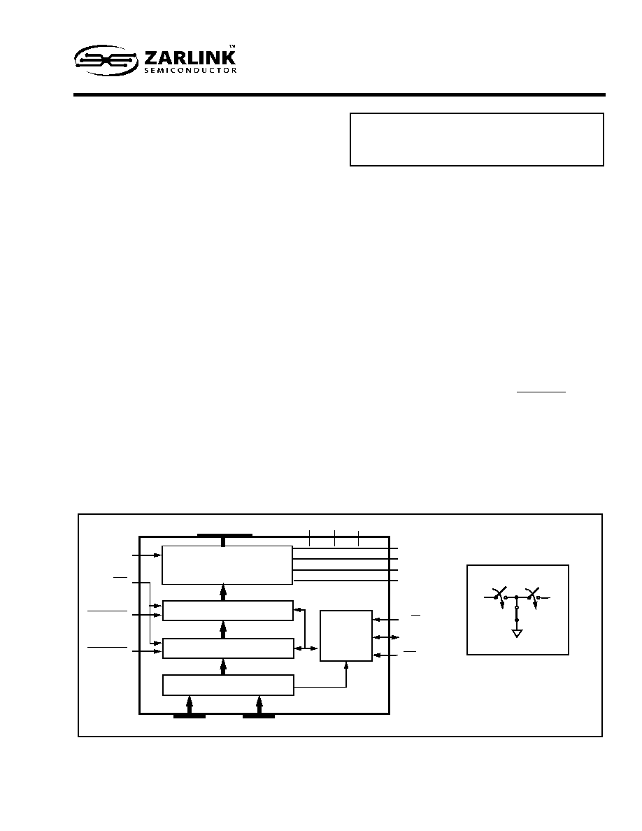
Each of the 32 nodes of the switching matrix has a T-
switch, see Fig.1. This grounds the nodes of all open
connections, which greatly reduces feedthrough
noise. In order to reduce crosstalk, individual analog
signal lines are isolated by interleaving them with
ground lines.
The two stage programmable latch system allows the
state of all switching nodes to be updated
simultaneously. The next state of the switch is written
into the first stage of the latches through individual
write cycles. These changes will not affect the
current state of the switch. The STROBE2
control
input is used to load the state of all first stage latches
to the second stage latches, which updates the
complete matrix. Therefore, all 32 switching nodes
are updated simultaneously.
The MT88V32 supports separate analog (V
EE
) and
digital (V
DD
) voltage references. This allows the user
to select an optimum analog signal bias point.
Ordering Information
MT88V32AP
44 Pin PLCC
-40
∞
to 85
∞
C
Figure 1 - Functional Block Diagram
Y0-Y7
VDD
VSS
X0
GND
MR
STROBE2
STROBE1
AX0-AX1
8x4
"T" Switch Array
VEE
2nd Stage Latches
1st Stage Latches
Address Decode
AY0-AY2
I/O
Logic
Control
X1
X2
X3
R/W
DATA
CS
Yi
Xi
GND
T-Switch Configuration
ISSUE 1
August 1993
MT88V32
8 x 4 High Performance Video Switch Array
Preliminary Information

MT88V32
Preliminary Information
3-52
Figure 2 - Pin Connections
Pin Description
Pin #*
Name
Description
1, 3, 4, 6,
8, 10, 12,
14, 16,
18, 20,
39, 41,
43
GND
Analog Ground.
Connect to system ground for crosstalk noise isolation. Pins 3 and 39
are not bonded internally.
2, 44,
42, 40
X0, X1,
X2, X3
Analog Lines (input/output)
.
5, 7,
9, 11,
13, 15,
17, 19
Y0, Y1,
Y2, Y3
Y4, Y5,
Y6, Y7
Analog Lines (input/output)
.
21
V
EE
Negative Analog Power Supply.
22
IC
Internal Connection.
23
V
DD
Positive Power Supply.
24
V
SS
Digital Ground Reference.
25, 26
AX1,AX0
X0-X3 I/O Address Select (inputs).
27, 30,31
AY2-AY0
Y0-Y7 I/O Address Select (inputs).
28, 29
NC
No Connection.
32
DATA
DATA (input/output)
. When input, a logic high will close the selected switch and a logic
low will open the selected switch. When output, a logic high indicates a closed switch
and a logic low indicates an opened switch.
33
CS
Chip Select (input).
Active low.
34
R/W
READ/WRITE Control (input).
When high the DATA pin is an output (for reading from
second stage latch); when low the DATA pin is an input (for writing to first stage latch).
35
STROBE1
STROBE 1 (input).
Modifies memory content of first stage latch as determined by the
addess and data lines, but does not change the switch array configuration of entire
switch array. Active low.
36
STROBE2
STROBE 2 (input).
Transfers memory content of first stage latch to the second stage
latch and hence, changes the configuration of entire switch array. Active low.
37
MR
MASTER RESET (input).
Used to reset the first and second stage latches. Active low.
38
NC
No Connection.
Y1
GND
Y2
GND
Y3
GND
Y4
GND
Y5
GND
Y6
GND
Y7
GND
VEE
IC*
VSS
AX1
AX0
AY2
NC
VDD
1
6 5 4 3 2
44 43 42 41 40
7
8
9
10
11
12
13
14
15
16
39
38
37
36
35
34
33
32
31
30
23
18 19 20 21 22
24 25 26 27 28
17
29
GND
NC
MR
STROBE2
STROBE1
R/W
CS
DATA
AY0
AY1
NC
X3
GND
X2
GND
X1
GND
X0
GND
GND
Y0
GND
* Connects toV
EE
Preliminary Information
MT88V32
3-53
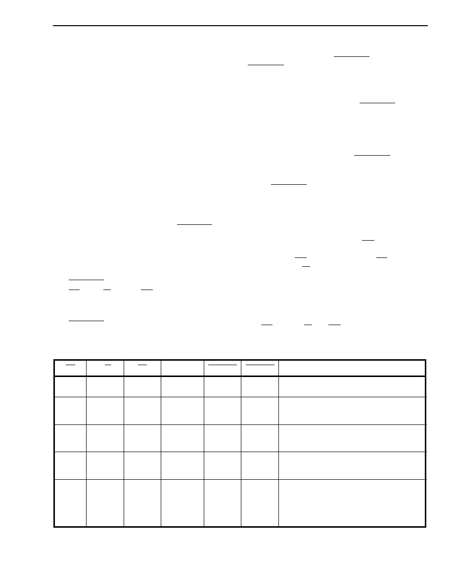
Functional Description
The state of the MT88V32 8 X 4 switching matrix is
updated through a simple parallel processor
interface. This interface provides access to 32 two
stage latches, which determines the state (open/
close) of each switching array node. Each latch (or
node) is addressed by the AX0-AX1 and AY0-AY2
inputs as per Table 2, and the DATA input will
determine if the connection is to be made (DATA=1)
or opened (DATA=0).
The second stage of the two stage latches controls
the current state of each switching node. The value
held in the first stage is the input to the second
stage. This allows the device to be programmed in
two ways. That is, individual switching nodes may be
updated one at a time, or all nodes may be updated
at once.
To update one node at a time the STROBE2 input
should be held low. This makes the second stage
latches transparent and the matrix immediately
reflects the state of the first stage latches. A write
cycle example follows:
1)
STROBE2
is low,
2)
CS
and R/W are low, MR
is high,
3)
AX0-AX1 and AY0-AY2 as per Table 2,
4)
DATA input high to close or low to open, and
5)
STROBE1
toggled from high-to-low-to-high.
These steps (one write cycle) may be repeated for
each switch state change. This can also be
accomplished by holding STROBE1
low and toggling
STROBE2. See Figure 14 for timing.
To update all nodes simultaneously all switch state
changes must be written into the first stage latches.
This is accomplished by holding STROBE2
high and
performing steps 2) through 5) above for each
switching node that is to be changed. Writing to the
first stage latches only will not affect the switching
state of the matrix. When the changes have been
made all the switches of the matrix may be updated
simultaneously by toggling the STROBE2
input from
high-to-low-to high.
When STROBE2
is used to update the state of the
MT88V32 all switch "breaks" are completed before
any switch "makes" occur. There is approximately
10ns delay between "breaks" and "makes".
Both the first and second stage latches will be
cleared when the master reset (MR) is taken from
high-to-low. This will open all the switch nodes. The
operation of MR
is independent of
CS, AX0-AX1,
AY0-AY2 and R/W.
The status of each switching array node (second
stage latch) can be read through the bidirectional
DATA pin. A read cycle example follows:
1) CS
is low, R/W and MR
are high,
2) AX0-AX1 and AY0-AY2 as per Table 2, and
3) DATA output high for closed or low for open.
Note:
x = don't care, 0 = logic "0" state, 1 = logic "1" state
A logic 1 on DATA input closes a connection.
A logic 0 on DATA input opens a connection.
MR
R/W
CS
DATA
STROBE1
STROBE2
DATA
1
1
0
0
1
0
0
1
1
0
1
0
1
1
No Change to 1st stage latch.
1st stage latch is loaded with data.
1
1
0
0
0
0
0
1
0
1
0
0
1
1
1st stage latch is transparent.
Selected latch is cleared and set again (i.e.,
output follows input).
1
1
0
0
0
x
1
x
0
1
1
1
1
0
1st stage latch output is frozen.
Output of 1st stage latch is transferred to
output of 2nd stage latches.
1
1
0
0
x
0
x
x
1
0
0
1
0
2nd stage latch output is frozen.
Both 1st stage and 2nd stage latches are
transparent.
1
0
1
1
0
1
0
1
x
1
x
1
DATA becomes an output and reflects the
contents of the 2nd stage latch addressed
by AX0-AX1 and AY0-AY2.
All crosspoints opened (data in 1st and 2nd
stage latches are cleared).
Table 1 - Truth Tables
MT88V32
Preliminary Information
3-54
It should be noted that the STROBE1
function is
disabled during a read cycle. See Fig. 15 for timing.
The MT88V32 can operate from a dual rail power
supply (V
DD
and V
EE
) or a single rail power supply
(V
SS
=V
EE
=0V) as per the recommended operating
conditions. For minimum on-state resistance the
supply voltages should be V
DD
=5.0 V
DC
, V
SS
=0 V
DC
and V
EE
=-7 V
DC
. The analog input signal should be
biased at -2.0 V
DC
to achieve minimum differential
phase and gain error (see AC Electrical
Characteristics - Crosspoint Performance).
Applications
Figure 3 illustrates examples of how to connect the
signal lines of the MT88V32 to various interfaces.
Input buffers allow the incoming signals to be scaled
and biased to the optimum operating range of the
MT88V32 (i.e., differential phase error, differential
gain error and R
ON
). Buffers will also allow a more
precise input impedance to be implemented. For low
grade video applications, signal lines may be
connected directly, as long as the ultimate source
and terminating impedances are matched.
Output buffers may be used to provide signal gain
and impedance matching for external connections.
Additionally, they may be used to isolate parasitic
device capacitance in multiple stage switching
applications where high frequency roll-off is critical.
Crosstalk, as well as differential phase and gain error
can be minimized by designing a low source
impedance (e.g., 10 ohms), and a high terminating
impedance (e.g., 10k) at each stage. If successive
switching stages are not buffered, then a resistor to
ground (R) should be present between the switches.
Selection of R is based on the following compromise:
1) as R is decreased to approach the source and
terminating resistance values signal loss will
increase and crosstalk will decrease, and
2) as R increases signal loss will decrease and
crosstalk will increase.
It is recommended that the power supply rails of the
MT88V32 be decoupled with 0.1
µ
F ceramic Z5U and
10
µ
F dipped tantalum capacitors. These capacitors
should be as close to the device as possible. The
signal pins of the MT88V32 are interleaved with
analog ground lines. This allows the circuit designer
to run ground tracks on both sides of each signal line
to improve crosstalk immunity.
The 8x4 bidirectional CMOS T-switch configuration is
a modular switching element in a convenient
package size. The inherent flexibility of this device
permits the designer to build large switching
matrices, see analog switch application notes.
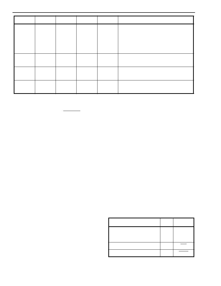
A
5
A
4
A
3
A
2
A
1
A
0
D
0
Function
0
0
0
1
0
1
0
1
0
1
0
1
1/0
1/0
Y0 to X0
Y7 to X3
1
X
X
X
X
0
X
MR
1
X
X
X
X
1
X
STB2
Table 3 - Address Decoding for the Processor
Interfaces
Note: x = undefined, 1/0 -1 = make, 0 = break
AX1
AX0
AY2
AY1
AY0
Switch Connections
0
0
0
0
0
0
0
0
0
0
0
0
0
0
0
0
0
0
0
0
1
1
1
1
0
0
1
1
0
0
1
1
0
1
0
1
0
1
0
1
Y0 to X0
Y1 to X0
Y2 to X0
Y3 to X0
Y4 to X0
Y5 to X0
Y6 to X0
Y7 to X0
0
0
1
1
0
1
0
1
0
1
Y0 to X1
Y7 to X1
1
1
0
0
0
1
0
1
0
1
Y0 to X2
Y7 to X2
1
1
1
1
0
1
0
1
0
1
Y0 to X3
Y7 to X3
Table 2 - Address Decode Truth Table

Preliminary Information
MT88V32
3-55
Figures 4, 5 and 6 show methods of interfacing the
MT88V32 to Motorola and Intel microcontrollers. The
address decoding for these configurations is in Table
3.
Video Signal Terminology
1) Component Video - separate red (R), blue (B),
green (G), and synchronization signals.
2) Composite Video - contains luminance
(brightness), chrominance (colour), and
synchronization signal components in a single
waveform.
3) Synchronization signal - horizontal sync pulses
are negative going excursions of the composite
video signal that occur every 63.5
µsec. Their
function is to align the horizontal sweep.
Vertical synchronization is achieved during the
vertical blanking interval, which is about 1200
µsec or 20 horizontal scan intervals long. It
consists of a number of vertical synchronization
and equalization pulses.
4) Luminance - is the black to white brightness
component of a composite video signal. Its range
is from reference white (maximum amplitude) to
reference black (minimum amplitude).
5) Chrominance - rides on the luminance signal and
determines the hue (phase) and brightness
(amplitude) of the colour component of a
composite video signal.
6) Colour burst - is about 9 (minimum 8) cycles of a
3.578545 MHz reference signal, which is
transmitted with every horizontal sweep of the
composite video signal. A phase comparison
Figure 3 - High Frequency Switching Applications
75
75
75
Wideband
Input Buffers
X0
X1
X2
X3
Y0
Y1
Y2
Y3
Y4
Y5
Y6
Y7
MT88V32
Control Interface
10k
10k
10k
Wideband
Output Buffers
75
75
75
10k
10k
10k
Wideband
Output Buffers
R
To next
switching
stage