 | –≠–ª–µ–∫—Ç—Ä–æ–Ω–Ω—ã–π –∫–æ–º–ø–æ–Ω–µ–Ω—Ç: MT8930C | –°–∫–∞—á–∞—Ç—å:  PDF PDF  ZIP ZIP |

1
Features
∑
ETS 300-012, CCITT I.430 and ANSI T1.605
S/T interface
∑
Full-duplex 2B+D, 192 kbit/s transmission
∑
Link activation/deactivation
∑
D-channel access contention resolution
∑
Point-to-point, point-to-multipoint and star
configurations
∑
Master (NT)/Slave (TE) modes of operation
∑
Exceeds loop length requirements
∑
Complete loopback testing capabilities
∑
On chip HDLC D-channel protocoller
∑
8 bit Motorola/Intel microprocessor interface
∑
Controllerless or microprocessor-controlled
operation
∑
Zarlink ST-BUS interface
∑
Low power CMOS technology
∑
Single 5 volt power supply
Applications
∑
ISDN NT1
∑
ISDN S or T interface
∑
ISDN Terminal Adaptor (TA)
∑
Digital sets (TE1) - 4 wire ISDN interface
∑
Digital PABXs, Digital Line Cards (NT2)
Description
The MT8930C Subscriber Network Interface Circuit
(SNIC) implements the ETSI ETS 300-012, CCITT
I.430 and ANSI T1.605 Recommendations for the
ISDN S and T reference points. Providing point-to-
point and point-to-multipoint digital transmission, the
SNIC may be used at either end of the subscriber
line (NT or TE).
An HDLC D-channel protocoller is included and
controlled through a Motorola/Intel microprocessor
port. A controllerless mode allows the SNIC to
operate without a microprocessor.
The MT8930C is fabricated in Zarlink's CMOS
process.
Figure 1 - Functional Block Diagram
DSTi
DSTo
F0od
C4b
F0b
STAR/Rsto
CK/NT
Cmode
LTx
VBias
LRx
V
DD
V
SS
ST-BUS
Interface
Timing
and
Control
D-channel Priority
Mechanism
PLL
HDLC
Transceiver
S-Bus
Link
Interface
Link
Activation
Controller
Microprocessor Interface
Rsti
HALF
AD0-7
R/W/WR,
AFT/PRI
DS/RD,
DinB
AS/ALE,
P/SC
CS,
DReq
IRQ/NDA,
DCack
Ordering Information
MT8930CE
28 Pin Plastic DIP
MT8930CP
44 Pin PLCC
-40
∞
C to +85
∞
C
ISSUE 3
November 1997
MT8930C
Subscriber Network Interface Circuit
CMOS ST-BUS
FAMILY
Data Sheet

MT8930C
Data Sheet
2
Figure 2 - Pin Connections
Pin Description
Pin #
Name
Description
DIP PLCC
1
2
HALF
HALF Input/Output: this is an input in NT mode and an output in TE mode identifying
which half of the S-interface frame is currently being written/read over the ST-BUS
(HALF = 0 sampled on the falling edge of C4b within the frame pulse low window,
identifies the information to be transmitted/received in the first half of the S-Bus frame
while HALF = 1 identifies the information to be transmitted/received into the second half
of the S-Bus frame). Tying this pin to V
SS
or V
DD
in NT mode will allow the device to
free run. This signal can also be accessed from the ST-BUS C-channel.
2
3
C4b
4.096 MHz Clock: a 4.096 MHz ST-BUS Data Clock input in NT mode.
In TE mode, a 4.096 MHz output clock phase-locked to the line data signal.
3
4
F0b
Frame Pulse: an active low frame pulse input indicating the beginning of active ST-
BUS channel times in NT mode. Frame pulse output in TE mode.
4
7
F0od
Delayed Frame Pulse Output: an active low delayed frame pulse output indicating
the end of active ST-BUS channels for this device. Can be used to daisy chain
to other ST-BUS devices to share an ST-BUS stream.
5
8
DSTi
Data ST-BUS Input: a 2048 kbit/s serial PCM/data ST-BUS input with D, C, B1, and B2
channels assigned to the first four timeslots. These channels contain data to be
transmitted on the line and chip control information.
6
9
DSTo
Data ST-BUS Output: a 2048 kbit/s serial PCM/data ST-BUS output with D, C, B1 and
B2 channels assigned to the first four timeslots respectively. The remaining timeslots
are placed into high impedance. These channels contain data received from the line
and chip status information.
7
13
Cmode
Controller Mode Select Input: when high, microprocessor control is selected. When
low the controllerless mode is enabled and the microport pins are redefined as control
inputs and status outputs.
8
14
CK/NT
TE Clock/Network Termination Mode Select Input. For TE mode, this pin must be
tied to V
SS
or to a 4.096 MHz clock (a clock is required for standard ISDN TE
applications). For NT mode, this pin must be tied to V
DD
. Refer to "ST-BUS Interface"
section for further explanation. A pull-up resistor is needed when driven by a TTL
device.
1
2
3
4
5
6
7
8
9
10
11
12
13
14
15
16
17
18
19
20
28
27
26
25
24
23
22
21
HALF
C4b
F0b
F0od
DSTi
DSTo
Cmode
CK/NT
R/W/WR, AFT/PRI
DS/RD, DinB
AS/ALE, P/SC
CS, DReq
IRQ/NDA, DCack
VSS
VDD
VBias
LTx
LRx
STAR/Rsto
Rsti
AD7, DR
AD6, AR
AD5, M/S
AD4, MCH
AD3, MFR
AD2, SYNC/BA
AD1, IS1
AD0, IS0
28 PIN PDIP
44 PIN PLCC
NC
NC
C4
b
F0b
HALF
VDD
VBi
as
LTx
NC
LRx
NC
STAR/Rsto
Rsti
NC
AD7, DR
AD6, AR
NC
AD5, M/S
AD4, MCH
AD3, MFR
NC
F0od
DSTi
DSTo
NC
NC
NC
Cmode
CK/NT
NC
R/W/WR, AFT/PRI
DS/RD, DinB
NC
AS/ALE, P/SC
CS
, DR
eq
IR
Q
/N
DA
, DCack
VSS
A
D
0, IS0
AD1, IS1
AD2
,
SY
NC/BA
NC
NC
NC
NC
1
6 5 4 3 2
44 43 42 41 40
7
8
9
10
11
12
13
14
15
16
39
38
37
36
35
34
33
32
31
30
23
18 19 20 21 22
24 25 26 27 28
17
29

Data Sheet
MT8930C
3
9
16
R/W
/
WR
AFT/PRI
Read/Write or Write Input (Cmode = 1): defines the data bus transfer as a read (R/
W=1) or a write (R/W=0) in Motorola bus mode. Redefined to WR in Intel bus mode.
Adaptive-Fixed Timing/Priority Select Input (Cmode=0): in NT mode, causes the
PLL and Rx filters and peak detectors to be disabled in favour of fixed timing and fixed
thresholds for short passive bus operation (0=fixed, 1=adaptive). In TE mode, this is the
Priority input. High priority (PRI=1) is normally reserved for signalling.
10
17
DS/RD
DinB
Data Strobe/Read Input (Cmode = 1): active high input indicates to the SNIC that
valid data is on the bus during a write operation or that the SNIC must output data
during a read operation in Motorola bus mode. Redefined to RD in Intel bus mode.
D-Channel in B1 Timeslot Input (Cmode = 0): active high input that causes all
eight ST-BUS D-channel bits, instead of the usual two bits, to be routed to and
from the S-interface B1 timeslot. When active, marks are transmitted in the
S-interface D-channel.
11
19
AS/ALE
P/SC
Address Strobe/Address Latch Enable Input (Cmode = 1): in Motorola bus mode
the falling edge is used to strobe the address into the SNIC during microprocessor
access. Redefined to ALE in Intel bus mode.
Parallel/Serial Control Input (Cmode = 0): determines if the serial C-channel
(P/SC=0) or microport pins (P/SC=1) are the source of chip control when controllerless
mode is selected. If the ST-BUS is chosen as the source, the dedicated Control input
pins are ignored but the status output pins remain valid.
12
20
CS
DReq
IC
Chip Select Input (Cmode=1): active low input used to select the SNIC for
microprocessor access.
D-Channel Request Input (Cmode = 0): an active high input that in TE mode only
causes the SNIC to transmit a "01111110" flag immediately if the D-channel is free, or
wait until it becomes available and then transmit the flag. The DCack signals the
successful acquisition of the D-channel. If DReq is tied low, continuous ones are
transmitted in the S-Bus D-channel.
Internal Connection (Cmode = 0): tie to V
SS
for normal operation in NT mode only.
13
21
IRQ
NDA
DCack
IC
Interrupt Request (Open Drain Output) (Cmode = 1): an output indicating an
unmasked HDLC interrupt. The interrupt remains active until the microprocessor clears
it by reading the HDLC Interrupt Status Register. This interrupt source is enabled with
B2=0 of Master Control Register.
New Data Available (Open Drain Output) (Cmode = 1): an active low output signal
indicating availability of new data from the S-Bus. This signal is selected with B2=1 of
Master Control Register.
D-Channel Acknowledge (Open Drain Output) (Cmode = 0): in TE mode only
indicates that the SNIC has gained access to the D-channel in response to a DReq and
has transmitted the first zero of an opening flag. The user should immediately begin
transmitting the rest of the packet over the ST-BUS D-channel. If this signal goes high
in the middle of transmission, the TE has lost the bus and must regain access of the D-
channel before retransmitting the packet.
Internal Connection (Open Drain Output) (C-mode=0). This pin is not used in NT
mode and should be left disconnected.
This pin must be tied to V
DD
with a 10k
resistor.
14
22
V
SS
Ground.
15-
22
24-26
30-32
34-35
AD0-7
Bidirectional Address/Data Bus (Cmode = 1): electrically and logically compatible to
either Intel or Motorola micro-bus specifications. If DS/RD is low on the rising edge of
AS/ALE then the chip operates to Motorola specs. If DS/RD is high on the rising edge
of AS/ALE Intel mode is selected. Taking Rsti low sets Motorola mode.
15-
16
24-
25
IS0-IS1
Internal State Outputs (Cmode =0): Binary encoded state number outputs.
IS0
IS1
NT Mode
TE Mode
0
0
deactivated
deactivated
0
1
pending deactivation
synchronized
1
0
pending activation
activation request
1
1
activated
activated
Pin Description (continued)
Pin #
Name
Description
DIP PLCC

MT8930C
Data Sheet
4
17
26
SYNC/BA Synchronization/Bus Activity Output (Cmode = 0): output indicating synchronization
to incoming RX frames when activation request is asserted and the deactivation request
is '0' (AR = 1 and DR = 0). Synchronization is declared once three successive frames
conforming to the 14-bit bipolar violation criteria have been detected. If part is
deactivated or activation request is '0' (AR = 0 or DR = 1), this pin indicates the
presence of bus activity.
18
30
MFR
Multiframe Input/Output (Cmode=0): multiframe input in NT mode or output in TE
mode. Setting this pin to one in NT mode when HALF = 1, forces the F
A
, N pair to 1, 0
respectively. This pin going high in TE mode indicates that F
A
= 1 & N= 0 has been
received. This signal is updated on the rising edge of the HALF signal.
19
31
MCH
Maintenance Channel (Q-channel) Input/Output (Cmode=0): an output in NT mode
which is valid only in the frame following the transmission of MFR. In TE mode, this is
the maintenance channel (Q-channel) input which is transmitted in the F
A
and L bits
following the reception of the multiframe signal. This input is sampled on the falling
edge of the HALF signal.
20
32
M/S
M/S Input/Output (Cmode=0): M/S bit input in NT mode or M/S bit output in TE mode.
M is read or written when HALF=1 while S is read or written when HALF=0.
21
34
AR
Activate Request Input (Cmode = 0): asserting AR with DR = 0 will initiate the
appropriate S-interface activation sequence coded in the NT or TE activation/
deactivation controller.
22
35
DR
Deactivate Request Input (Cmode = 0): asserting DR high will initiate the appropriate
S-interface deactivation sequence coded in the NT or TE activation/ deactivation
controller.
23
37
Rsti
Reset Input: Schmitt trigger reset input. If '0', sets all control registers to the default
conditions, resets activation state machines to the deactivated state, resets HDLC,
clears the HDLC FIFO`s. Sets the microport to Motorola bus mode.
24
38
STAR/Rsto Star/Reset (Open Drain Output): 192kbit/s Rx data output fixed relative to the ST-BUS
timebase. A group of NTs, in fixed timing mode, can be wire or'ed together to create a
Star configuration. Active low reset output in TE mode indicating 128 consecutive
marks have been received. Can be connected directly to Rsti to allow NT to reset all
TEs on the bus. This pin must be tied to V
DD
with a 10 k
resistor.
25
40
LRx
Receive Line Signal Input: this is a high impedance input for the pseudoternary line
signal to be connected to the line through a 2:1 ratio transformer. See Figures 20 and
21. A DC bias level on this input equal to V
Bias
must be maintained.
26
42
LTx
Transmit Line Signal Output: this is a current source output designed to drive a
nominal 50 ohm line through a 2:1 ratio transformer. See Figures 20 and 21.
27
43
V
Bias
Bias Voltage: analog ground for Tx and Rx transformers. This pin must be decoupled
to V
DD
through a 10
µ
F capacitor with good high frequency characteristics (i.e.,
tantalum).
28
44
V
DD
Power Supply Input.
1,5-6,10-
12,15,18,
23,27-29,
33, 36,
39, 41
NC
No Connection.
Pin Description (continued)
Pin #
Name
Description
DIP PLCC
Data Sheet
MT8930C
5
Functional Description
The MT8930C Subscriber Network Interface Circuit
(SNIC) is a multifunction transceiver providing a
complete interface to the S/T Reference Point as
specified in ETS 300-012, CCITT Recommendation
I.430 and ANSI T1.605. Implementing both
point-to-point and point-to-multipoint voice/data
transmission, the SNIC may be used at either end of
the digital subscriber loop. A programmable digital
interface allows the MT8930C to be configured as a
Network Termination (NT) or as a Terminal
Equipment (TE) device.
The SNIC supports 192 kbit/s (2B+D + overhead) full
duplex data transmission on a 4-wire balanced
transmission line. Transmission capability for both B
and D channels, as well as related timing and
synchronization functions, are provided on chip. The
signalling capability and procedures necessary to
enable customer terminals (TEs) to be activated and
deactivated, form part of the MT8930C's
functionality. The SNIC handles D-channel resource
allocation and prioritization for access contention
resolution and signalling requirements in passive bus
line configurations. Control and status information
allows implementation of maintenance functions and
monitoring of the device and the subscriber loop.
An HDLC transceiver is included on the SNIC for link
access protocol handling via the D-channel.
Depacketized data is passed to and from the
transceiver via the microprocessor port. Two 19 byte
deep FIFOs, one for transmit and one for receive,
are provided to buffer the data. The HDLC block can
be set up to transmit or receive to/from either the
S-interface port or the ST-BUS port. Further, the
transmit destination and receive source can be
independently selected, e.g., transmit to S-interface
while receiving from ST-BUS. The transmit and
receive paths can be separately enabled or disabled.
Both, one and two byte address recognition is
supported by the SNIC. A transparent mode allows
data to be passed directly to the D channel without
being packetized.
A block diagram of the MT8930C is shown in Figure
1. The SNIC has three interface ports: a 4-wire
CCITT compatible S/T interface (subscriber loop
interface), a 2048 kbit/s ST-BUS serial port, and a
general purpose parallel microprocessor port. This
8-bit parallel port is compatible with both Motorola or
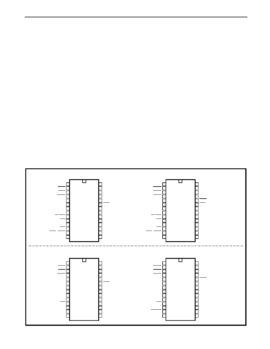
Figure 3 - SNIC Pin Connections in Various Modes
1
2
3
4
5
6
7
8
9
10
11
12
13
14
15
16
17
18
19
20
28
27
26
25
24
23
22
21
HALF
C4bi
F0bi
F0od
DSTi
DSTo
Cmode
NT
R/W/WR
DS/RD
AS/ALE
CS
IRQ, NDA
VSS
VDD
VBias
LTx
LRx
STAR
Rsti
AD7
AD6
AD5
AD4
AD3
AD2
AD1
AD0
1
2
3
4
5
6
7
8
9
10
11
12
13
14
15
16
17
18
19
20
28
27
26
25
24
23
22
21
HALF
C4bo
F0bo
F0od
DSTi
DSTo
Cmode
CK
R/W/WR
DS/RD
AS/ALE
CS
IRQ, NDA
VSS
VDD
VBias
LTx
LRx
Rsto
Rsti
AD7
AD6
AD5
AD4
AD3
AD2
AD1
AD0
1
2
3
4
5
6
7
8
9
10
11
12
13
14
15
16
17
18
19
20
28
27
26
25
24
23
22
21
HALF
C4bi
F0bi
F0od
DSTi
DSTo
Cmode
NT
AFT
DinB
P/SC
IC
IC
VSS
VDD
VBias
LTx
LRx
STAR
Rsti
DR
AR
M/Si
MCHo
MFRi
SYNC/BA
IS1
IS0
1
2
3
4
5
6
7
8
9
10
11
12
13
14
15
16
17
18
19
20
28
27
26
25
24
23
22
21
HALF
C4bo
F0bo
F0od
DSTi
DSTo
Cmode
CK
PRI
DinB
P/SC
DReq
DCack
VSS
VDD
VBias
LTx
LRx
Rsto
Rsti
DR
AR
M/So
MCHi
MFRo
SYNC/BA
IS1
IS0
NT MODE
NT MODE
TE MODE
TE MODE
CONTROLLER MODE
CONTROLLERLESS MODE