 | –≠–ª–µ–∫—Ç—Ä–æ–Ω–Ω—ã–π –∫–æ–º–ø–æ–Ω–µ–Ω—Ç: MT8931CPR | –°–∫–∞—á–∞—Ç—å:  PDF PDF  ZIP ZIP |

1
Features
∑
ETS 300-012, CCITT I.430 and ANSI T1.605
S/T interface
∑
Full-duplex 2B+D, 192 kbit/s transmission
∑
Link activation/deactivation
∑
D-channel access contention resolution
∑
Point-to-point, point-to-multipoint and star
configurations
∑
Master (NT)/Slave (TE) modes of operation
∑
Exceeds loop length requirements
∑
Complete loopback testing capabilities
∑
On chip HDLC D-channel protocoller
∑
8 bit Motorola/Intel microprocessor interface
∑
Microprocessor-controlled operation
∑
Zarlink ST-BUS interface
∑
Low power CMOS technology
∑
Single 5 volt power supply
Applications
∑
ISDN NT1
∑
ISDN S or T interface
∑
ISDN Terminal Adaptor (TA)
∑
Digital sets (TE1) - 4 wire ISDN interface
∑
Digital PABXs, Digital Line Cards (NT2)
Description
The MT8931C Subscriber Network Interface Circuit
(SNIC) implements the ETSI ETS 300-012, CCITT
I.430 and ANSI T1.605 Recommendations for the
ISDN S and T reference points. Providing point-to-
point and point-to-multipoint digital transmission, the
SNIC may be used at either end of the subscriber
line (NT or TE).
An HDLC D-channel protocoller is included and
controlled through a Motorola/Intel microprocessor
port.
The MT8931C is fabricated in Zarlink's CMOS
process.
Figure 1 - Functional Block Diagram
DSTi
DSTo
F0od
C4b
F0b
STAR/Rsto
XTAL1/NT
XTAL2/NC
LTx
VBias
LRx
VDD
VSS
ST-BUS
Interface
Timing
and
Control
D-channel Priority
Mechanism
PLL
HDLC
Transceiver
S-Bus
Link
Interface
Link
Activation
Controller
Microprocessor Interface
Rsti
HALF
AD0-7
R/W/WR
DS/RD
AS/ALE
CS
IRQ/NDA
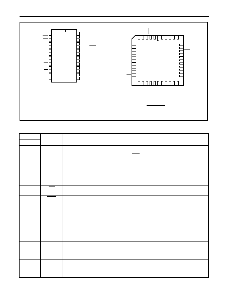
Ordering Information
MT8931CE
28 Pin Plastic DIP
MT8931CP
44 Pin PLCC
-40
∞
C to +85
∞
C
ISSUE 4
November 1997
MT8931C
Subscriber Network Interface Circuit
CMOS ST-BUS
FAMILY
Data Sheet
MT8931C
Data Sheet
2
Figure 2 - Pin Connections
Pin Description
Pin #
Name
Description
DIP PLCC
1
2
HALF
HALF Input/Output: this is an input in NT mode and an output in TE mode identifying
which half of the S-interface frame is currently being written/read over the ST-BUS
(HALF = 0 sampled on the falling edge of C4b within the frame pulse low window,
identifies the information to be transmitted/received in the first half of the S-Bus frame
while HALF=1 identifies the information to be transmitted/received into the second half
of the S-Bus frame). Tying this pin to V
SS
or V
DD
in NT mode will allow the device to free
run. This signal can also be accessed from the ST-BUS C-channel.
2
3
C4b
4.096 MHz Clock: a 4.096 MHz ST-BUS Data Clock input in NT mode.
In TE mode an output 4.096 MHz clock phase-locked to the line data signal.
3
4
F0b
Frame Pulse: an active low frame pulse input indicating the beginning of active ST-
BUS channel times in NT mode. Frame pulse output in TE mode.
4
7
F0od
Delayed Frame Pulse Output: an active low delayed frame pulse output indicating
the end of active ST-BUS channels for this device. Can be used to daisy chain
to other ST-BUS devices to share an ST-BUS stream.
5
8
DSTi
Data ST-BUS Input: a 2048 kbit/s serial PCM/data ST-BUS input with D, C, B1, and B2
channels assigned to the first four timeslots. These channels contain data to be
transmitted on the line and chip control information.
6
9
DSTo
Data ST-BUS Output: a 2048 kbit/s serial PCM/data ST-BUS output with D, C, B1 and
B2 channels assigned to the first four timeslots, respectively. The remaining timeslots
are placed into high impedance. These channels contain data received from the line
and chip status information.
7
13
XTAL2/IC Crystal 2/Internal Connection: in TE mode, XTAL1 and XTAL2 are to be connected to
an external 4.096 MHz parallel resonant crystal for the on-chip oscillator.
If XTAL1 is connected directly to a 4.096 MHz clock, this pin must be left unconnected.
In NT mode, this pin must be left unconnected.
8
14
XTAL1/NT Crystal 1/Network Termination Mode Select Input: for TE mode mode selection, a
4.096 MHz crystal is to be connected between the XTAL1 and XTAL2 pins, or a 4.096
MHz clock can be connected directly to XTAL1. For NT mode selection, this pin must
be tied to VDD. A pull-up resistor is needed when driven by a TTL device.
1
2
3
4
5
6
7
8
9
10
11
12
13
14
15
16
17
18
19
20
28
27
26
25
24
23
22
21
HALF
C4b
F0b
F0od
DSTi
DSTo
XTAL2/NC
XTAL1/NT
R/W/WR
DS/RD
AS/ALE
CS
IRQ/NDA
VSS
VDD
VBias
LTx
LRx
STAR/Rsto
Rsti
AD7
AD6
AD5
AD4
AD3
AD2
AD1
AD0
28 PIN PDIP
44 PIN PLCC
NC
NC
C4
b
F0
b
HALF
VDD
VBi
as
LT
x
NC
LR
x
NC
STAR/Rsto
Rsti
NC
AD7
AD6
NC
AD5
AD4
AD3
NC
F0od
DSTi
DSTo
NC
NC
NC
XTAL2/NC
XTAL1/NT
NC
R/W/WR
DS/RD
NC
AS/ALE
CS
IRQ
/NDA
VS
S
AD0
AD1
AD2
NC
NC
NC
NC
1
6 5 4 3 2
44 43 42 41 40
7
8
9
10
11
12
13
14
15
16
39
38
37
36
35
34
33
32
31
30
23
18 19 20 21 22
24 25 26 27 28
17
29

Data Sheet
MT8931C
3
9
16
R/W
/
WR Read/Write or Write Input: defines the data bus transfer as a read (R/W=1) or a write
(R/W=0) in Motorola bus mode. Redefined to WR in Intel bus mode.
10
17
DS/RD
Data Strobe/Read Input: active high input indicates to the SNIC that valid data is on
the bus during a write operation or that the SNIC must output data during a read
operation in Motorola bus mode. Redefined to RD in Intel bus mode.
11
19
AS/ALE
Address Strobe/Address Latch Enable Input: in Motorola bus mode the falling edge
is used to strobe the address into the SNIC during microprocessor access. Redefined
to ALE in Intel bus mode.
12
20
CS
Chip Select Input: active low, used to select the SNIC for microprocessor access.
13
21
IRQ
NDA
Interrupt Request (Open Drain Output): an output indicating an unmasked HDLC
interrupt. The interrupt remains active until the microprocessor clears it by reading the
HDLC Interrupt Status Register. This interrupt source is enabled with B2=0 of Master
Control Register.
New Data Available (Open Drain Output): an active low output signal indicating
availability of new data from the S-Bus. This signal is selected with B2=1 of Master
Control Register. This pin must be tied to V
DD
with a 10k
resistor.
14
22
V
SS
Ground.
15-
22
24-26,
30-32,
34-35
AD0-7
Bidirectional Address/Data Bus: electrically and logically compatible to either Intel or
Motorola micro-bus specifications. If DS/RD is low on the rising edge of AS/ALE then
the chip operates to Motorola specs. If DS/RD is high on the rising edge of AS/ALE Intel
mode is selected. Taking Rsti low sets Motorola mode.
23
37
Rsti
Reset Input: Schmitt trigger reset input. If '0', sets all control registers to the default
conditions, resets activation state machines to the deactivated state, resets HDLC,
clears the HDLC FIFO`s. Sets the microport to Motorola bus mode.
24
38
STAR/Rsto Star/Reset (Open Drain Output): 192kbit/s Rx data output fixed relative to the ST-BUS
timebase. A group of NTs, in fixed timing mode, can be wire or'ed together to create a
Star configuration. Active low reset output in TE mode indicating 128 consecutive
marks have been received. Can be connected directly to Rsti to allow NT to reset all
TEs on the bus. This pin must be tied to V
DD
with a 10 k
resistor.
25
40
LRx
Receive Line Signal Input: this is a high impedance input for the pseudoternary line
signal to be connected to the line through a 2:1 ratio transformer. See Figures 20 and
21. A DC bias level on this input equal to V
Bias
must be maintained.
26
42
LTx
Transmit Line Signal Output: this is a current source output designed to drive a
nominal 50 ohm line through a 2:1 ratio transformer. See Figures 20 and 21.
27
43
V
Bias
Bias Voltage: analog ground for Tx and Rx transformers. This pin must be decoupled
to V
DD
through a 10
µ
F capacitor with good high frequency characteristics.
28
44
V
DD
Power Supply Input.
1,5-6,10-
12,15,18,
23,27-29,
33, 36,
39, 41
NC
No Connection.
Pin Description (continued)
Pin #
Name
Description
DIP PLCC
MT8931C
Data Sheet
4
Functional Description
The MT8931C Subscriber Network Interface Circuit
(SNIC) is a multifunction transceiver providing a
complete interface to the S/T Reference Point as
specified in ETS 300-012, CCITT Recommendation
I.430 and ANSI T1.605. Implementing both
point-to-point and point-to-multipoint voice/data
transmission, the SNIC may be used at either end of
the digital subscriber loop. A programmable digital
interface allows the MT8931C to be configured as a
Network Termination (NT) or as a Terminal
Equipment (TE) device.
The SNIC supports 192 kbit/s (2B+D + overhead) full
duplex data transmission on a 4-wire balanced
transmission line. Transmission capability for both B
and D channels, as well as related timing and
synchronization functions, are provided on chip. The
signalling capability and procedures necessary to
enable customer terminals (TEs) to be activated and
deactivated, form part of the MT8931C's
functionality. The SNIC handles D-channel resource
allocation and prioritization for access contention
resolution and signalling requirements in passive bus
line configurations. Control and status information
allows implementation of mainten-ance functions
and monitoring of the device and the subscriber loop.
An HDLC transceiver is included on the SNIC for link
access protocol handling via the D-channel.
Depacketized data is passed to and from the
transceiver via the microprocessor port. Two 19 byte
deep FIFOs, one for transmit and one for receive,
are provided to buffer the data. The HDLC block can
be set up to transmit or receive to/from either the
S-interface port or the ST-BUS port. Further, the
transmit destination and receive source can be
independently selected, e.g., transmit to S-interface
while receiving from ST-BUS. The transmit and
receive paths can be separately enabled or disabled.
Both, one and two byte address recognition is
supported by the SNIC. A transparent mode allows
data to be passed directly to the D channel without
being packetized.
A block diagram of the MT8931C is shown in Figure
1. The SNIC has three interface ports: a 4-wire
CCITT compatible S/T interface (subscriber loop
interface), a 2048 kbit/s ST-BUS serial port, and a
general purpose parallel microprocessor port. This
8-bit parallel port is compatible with both Motorola or
Intel microprocessor bus signals and timing.
The three major blocks of the MT8931C, consisting
of the system serial interface (ST-BUS), HDLC
transceiver, and the digital subscriber loop interface
(S-interface) are interconnected by high speed data
busses. Data sent to and received from the
S-interface port (B1, B2 and D channels) can be
accessed from either the parallel microprocessor
port or the serial ST-BUS port. This is also true for
SNIC control and status information (C-channel).
Depacketized D-channel information to and from the
HDLC section can only be accessed through the
parallel microprocessor port.
S-Bus Interface
The S-Bus is a four wire, full duplex, time division
multiplexed transmission facility which exchanges
information at 192 kbit/s rate including two 64 kbit/s
PCM voice or data channels, a 16 kbit/s signalling
channel and 48 kbit/s for synchronization and
overhead. The relative position of these channels
with respect to the ST-BUS is shown in Figures 4
and 5.
The SNIC makes use of the first four channels on the
ST-BUS to transmit and receive control/status and
data to and from the S-interface port. These are the
B, D and C-channels (see Figure 4).
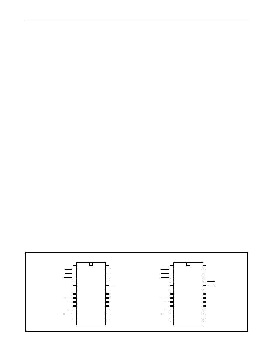
Figure 3 - SNIC Pin Connections
1
2
3
4
5
6
7
8
9
10
11
12
13
14
15
16
17
18
19
20
28
27
26
25
24
23
22
21
HALF
C4bi
F0bi
F0od
DSTi
DSTo
Cmode
NT
R/W/WR
DS/RD
AS/ALE
CS
IRQ/NDA
VSS
VDD
VBias
LTx
LRx
STAR
Rsti
AD7
AD6
AD5
AD4
AD3
AD2
AD1
AD0
1
2
3
4
5
6
7
8
9
10
11
12
13
14
15
16
17
18
19
20
28
27
26
25
24
23
22
21
HALF
C4bo
F0bo
F0od
DSTi
DSTo
XTAL2
XTAL1
R/W/WR
DS/RD
AS/ALE
CS
IRQ/NDA
VSS
VDD
VBias
LTx
LRx
Rsto
Rsti
AD7
AD6
AD5
AD4
AD3
AD2
AD1
AD0
NT MODE
TE MODE
Data Sheet
MT8931C
5
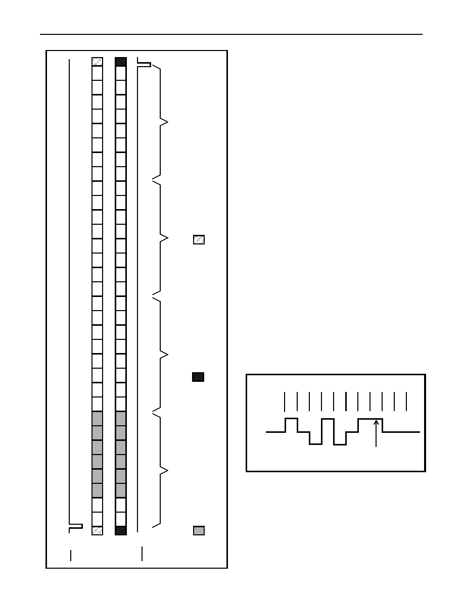
Figure 4 - ST-BUS Channel Assignment
D
0
D
1
D
2
D3
D4
D5
D6
D7
D
0
D
1
D
2
D3
D4
D5
D6
D7
C7
C6
C5
C4
C3
C2
C1
C0
C7
C6
C5
C4
C3
C2
C1
C0
B1
B1
B
1
B
1
B
1
B1
B1
B1
B2
B2
B2
B2
B2
B2
B
2
B
2
B1
B1
B
1
B
1
B
1
B1
B1
B1
B2
B2
B2
B2
B2
B2
B
2
B
2
C
h
a
n
n
e
l
1
(C)
C
han
nel 2
(B1)
C
hannel 3 (B2)
C
hannel 0 (D
)
Only
valid
with
64 kb
it/s D-channe
l
O
utp
u
t in h
i
gh impedance state
D
on't care
F0b
DST
i
DST
o
F0o
d
The B1 and B2 channels each have a bandwidth of
64 kbit/s and are used to carry PCM voice or data
across the network.
The D-channel is primarily intended to carry
signalling information for circuit switching through
the ISDN network. The SNIC provides the capability
of having a 16 kbit/s or full 64 kbit/s D-channel by
allocating the B1-channel timeslot to the D-channel.
Access to the depacketized D-channel is only
granted through the parallel microprocessor port.
The C-channel provides a means for the system to
control and monitor the functionality of the SNIC.
This control/status channel is accessed by the
system through the ST-BUS or microprocessor port.
The C-channel provides access to two registers
which provide complete control over the state
activation machine, the D-channel priority
mechanism as well as the various maintenance
functions. A detailed description of these registers is
discussed in the microprocessor port interface.
Line Code
The line code used on the S-interface is a Pseudo
ternary code with 100% pulse width as seen in
Figure 5 below. Binary zeros are represented as
marks on the line and successive marks will
alternate in polarity.
Figure 5 - Alternate Zero Inversion Line Code
A mark which does not adhere to the alternating
polarity is known as a bipolar violation.
BINARY
VALUE
LINE
SIGNAL
Violation
0
1
0
0
0
1
0
0
1
1