 | –≠–ª–µ–∫—Ç—Ä–æ–Ω–Ω—ã–π –∫–æ–º–ø–æ–Ω–µ–Ω—Ç: MT8961 | –°–∫–∞—á–∞—Ç—å:  PDF PDF  ZIP ZIP |
Document Outline
- Features
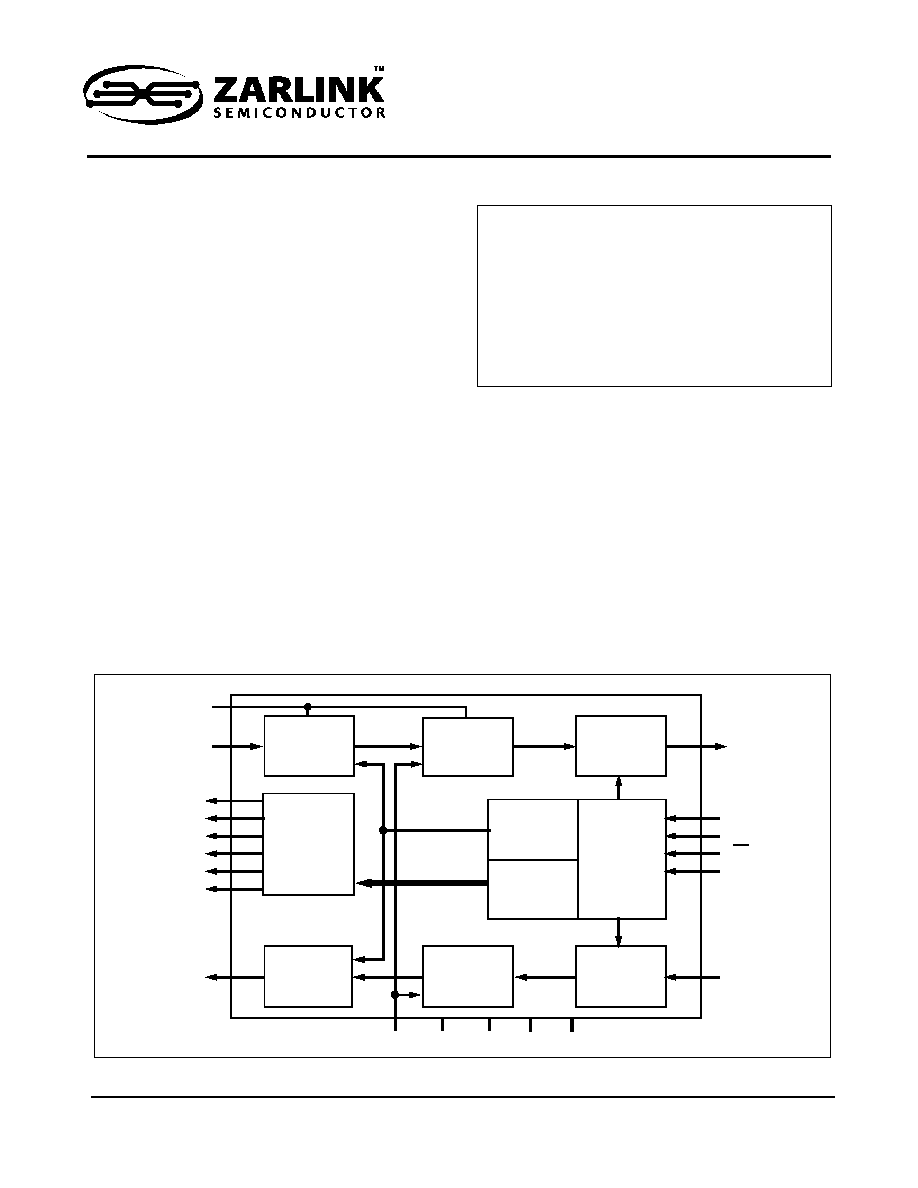
- Figure 1 - Functional Block Diagram
- Description
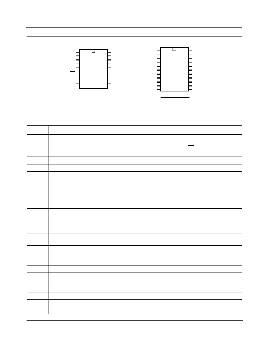
- Figure 2 - Pin Connections
- Pin Description
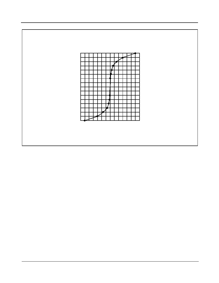
- Figure 3 - m-Law Encoder Transfer Characteristic
- Figure 4 - A-Law Encoder Transfer Characteristic
- Functional Description
- Transmit Path
- Receive Path
- VRef
- Figure 5 - Typical Voltage Reference Circuit
- Timing
- Digital Control Functions
- Mode 1
- Mode 2
- Mode 3
- Table 1 - Digital Control Modes
- Table 2 - Control States - Register A
- Control Registers A, B
- Chip Testing
- Loopback
- Logic Control Outputs SD0-5
- Figure 6 - Typical Line Termination
- Table 3 - Control States - Register B
- Powerdown
- Figure 7 - Typical Use of the Special Drive Outputs
- Figure 8 - Example Architecture of a Simple Digital Switching System using the MT8960-67
- Absolute Maximum Ratings*
- Recommended Operating Conditions - Voltages are with respect to GNDD unless otherwise stated
- DC Electrical Characteristics - Voltages are with respect to GNDD unless otherwise stated.
- TA=0 to 70∞C, VDD=5V±5%, VEE=-5V±5%, VRef=2.5V±0.5%, GNDA=GNDD=0V,Clock Frequency =2.048MHz. Outp...
- AC Electrical Characteristics - Voltages are with respect to GNDD unless otherwise stated.
- TA=0 to 70∞C, VDD=5V±5%, VEE=-5V±5%, VRef=2.5V±0.5%, GNDA=GNDD=0V, Clock Frequency=2.048 MHz. Out...
- AC Electrical Characteristics - Transmit (A/D) Path - Voltages are with respect to GNDD unless ot...
- TA=0 to 70∞C, VDD=5V±5%, VEE=-5V±5%, VRef=2.5V±0.5%, GNDA=GNDD=0V, Clock Frequency = 2.048MHz,
- Filter Gain Setting = 0dB. Outputs unloaded unless otherwise specified.
- AC Electrical Characteristics - Receive (D/A) Path - Voltages are with respect to GNDD unless oth...
- TA=0 to 70∞C, VDD=5V±5%, VEE=-5V±5%, VRef=2.5V±0.5%, GNDA=GNDD=0V, Clock Frequency = 2.048MHz,
- Filter Gain Setting = 0dB. Outputs unloaded unless otherwise specified.
- Figure 10 - Attenuation vs Frequency for Transmit (A/D) Filter
- Figure 11 - Attenuation vs Frequency for Receive (D/A) Filter
- Figure 12 - Variation of Gain With Input Level
- Figure 13 - Signal to Total Distortion Ratio vs Input Level
- Figure 14 - Envelope Delay Variation Frequency
- Figure 15 - Overload Distortion (End-to-End)
1
Zarlink Semiconductor Inc.
Zarlink, ZL and the Zarlink Semiconductor logo are trademarks of Zarlink Semiconductor Inc.
Copyright 2003-2005, Zarlink Semiconductor Inc. All Rights Reserved.
Features
∑ ST-BUS
compatible
∑ Transmit/Receive filters & PCM Codec in one I.C
∑ Meets AT&T D3/D4 and CCITT G711 and G712
∑
µ-Law: MT8960/62/64/67
∑ A-Law: MT8961/63/65/67
∑ Low power consumption:
Op.: 30 mW typ.
Stby.: 2.5 mW typ.
∑ Digital Coding Options:
MT8964/65/66/67 CCITT Code
MT8960/61/62/63 Alternative Code
∑ Digitally controlled gain adjust of both filters
∑ Analog and digital loopback
∑ Filters and codec independently user accessible
for testing
∑ Powerdown mode available
∑ 2.048 MHz master clock input
∑ Up to six uncommitted control outputs
∑
±5 V ±5% power supply
Description
Manufactured in ISO
2
-CMOS, these integrated
filter/codecs are designed to meet the demanding
performance needs of the digital telecommunications
industry, e.g., PABX, Central Office, Digital telephones.
February 2005
Ordering Information
MT8960/61/64/65AE
18 Pin PDIP
Tubes
MT8962/63AE
20 Pin PDIP
Tubes
MT8962/63/66/67AS
20 Pin SOIC
Tubes
MT8963ASR
20 Pin SOIC
Tape & Reel
MT8960AE1
18 Pin PDIP*
Tubes
MT8962/63AE1
20 Pin PDIP*
Tubes
MT8962AS1
20 Pin SOIC*
Tubes
MT8963AS1
20 Pin SOIC*
Tubes
*Pb Free Matte Tin
-40
∞C to +85∞C
ISO
2
-CMOS
MT8960/61/62/63/64/65/66/67
Integrated PCM Filter Codec
Data Sheet
Figure 1 - Functional Block Diagram
ANUL
V
X
SD0
SD1
SD2
SD3
SD4
SD5
V
R
V
Ref
GNDA GNDD V
DD
V
EE
DSTo
CSTi
CA
F1i
C2i
DSTi
Transmit
Filter
Output
Register
Receive
Filter
Analog to
Digital PCM
Encoder
PCM Digital
to Analog
Decoder
Output
Register
Input
Register
A Register
8-Bits
B-Register
8-Bits
Control
Logic
MT8960/61/62/63/64/65/66/67
Data Sheet
2
Zarlink Semiconductor Inc.
Figure 2 - Pin Connections
Pin Description
Pin Name
Description
CSTi
Control ST-BUS In is a TTL-compatible digital input used to control the function of the filter/codec.
Three modes of operation may be effected by applying to this input a logic high (V
DD
), logic low
(GNDD), or an 8-bit serial word, depending on the logic states of CA and F1i.
Functions controlled are: powerdown, filter gain adjust, loopback, chip testing, SD outputs.
DSTi
Data ST-BUS In accepts the incoming 8-bit PCM word. Input is TTL-compatible.
C2i
Clock Input is a TTL-compatible 2.048 MHz clock.
DSTo
Data ST-BUS Out is a three-state digital output driving the PCM bus with the outgoing 8-bit PCM
word.
V
DD
Positive power Supply (+5 V).
F1i
Synchronization Input
is an active low digital input enabling (in conjunction with CA) the PCM input,
PCM output and digital control input. It is internally sampled on every positive edge of the clock, C2i,
and provides frame and channel synchronization.
CA
Control Address is a three-level digital input which enables PCM input and output and determines
into which control register (A or B) the serial data, presented to CSTi, is stored.
SD3
System Drive Output is an open drain output of an N-channel transistor which has its source tied to
GNDA. Inactive state is open circuit.
SD4-5
System Drive Outputs
are
open drain outputs of N-channel transistors which have their source tied
to GNDD. Inactive state is open circuit.
SD0-2
System Drive Outputs
are
"Totempole" CMOS outputs switching between GNDD and V
DD
. Inactive
state is logic low.
V
EE
Negative power supply (-5 V).
V
X
Voice Transmit
is the
analog input to the transmit filter.
ANUL
Auto Null
is used to integrate an internal auto-null signal.
A 0.1
µF capacitor must be connected
between this pin and GNDA.
V
R
Voice Receive
is the
analog output of the receive filter.
GNDA
Analog ground (0 V).
V
Ref
Voltage Reference input to D to A converter.
GNDD
Digital ground (0 V).
1
2
3
4
5
6
7
8
9
10
11
12
20
19
18
17
16
15
14
13
20 PIN PDIP/SOIC
CSTi
DSTi
C2i
DSTo
VDD
SD5
SD4
F1i
CA
SD3
GNDD
VRef
GNDA
VR
ANUL
VX
VEE
SD0
SD1
SD2
1
2
3
4
5
6
7
8
9
10
18
17
16
15
14
13
12
11
18 PIN PDIP
CSTi
DSTi
C2i
DSTo
VDD
F1i
CA
SD3
SD2
GNDD
VRef
GNDA
VR
ANUL
VX
VEE
SD0
SD1
MT8960/61/64/65
MT8962/63/66/67

MT8960/61/62/63/64/65/66/67
Data Sheet
3
Zarlink Semiconductor Inc.
Figure 3 -
µ-Law Encoder Transfer Characteristic
11111111
11110000
11100000
11010000
11000000
10110000
10100000
10010000
10000000
00000000
00010000
00100000
00110000
01000000
01010000
01100000
01110000
01111111
10000000
10001111
10011111
10101111
10111111
11001111
11011111
11101111
11111111
01111111
01101111
01011111
01001111
00111111
00101111
00011111
00001111
00000000
-2.415V -1.207V
0V
+1.207V +2.415V
Bit 7... 0
MSB LSB
Analog Input Voltage (V
IN
)
MT8960/62
Digital Output
MT8964/66
Digital Output
MT8960/61/62/63/64/65/66/67
Data Sheet
4
Zarlink Semiconductor Inc.
Figure 4 - A-Law Encoder Transfer Characteristic
Functional Description
Figure 1 shows the functional block diagram of the MT8960-67. These devices provide the conversion interface
between the voiceband analog signals of a telephone subscriber loop and the digital signals required in a digital
PCM (pulse code modulation) switching system. Analog (voiceband) signals in the transmit path enter the chip at
V
X
, are sampled at 8 kHz, and the samples quantized and assigned 8-bit digital values defined by logarithmic PCM
encoding laws. Analog signals in the receive path leave the chip at V
R
after reconstruction from digital 8-bit words.
Separate switched capacitor filter sections are used for bandlimiting prior to digital encoding in the transmit path
and after digital decoding in the receive path. All filter clocks are derived from the 2.048 MHz master clock input,
C2i. Chip size is minimized by the use of common circuitry performing the A to D and D to A conversion. A
successive approximation technique is used with capacitor arrays to define the 16 steps and 8 chords in the signal
conversion process. Eight-bit PCM encoded digital data enters and leaves the chip serially on DSTi and DSTo
pins, respectively.
Transmit Path
Analog signals at the input (Vx) are firstly bandlimited to 508 kHz by an RC lowpass filter section. This performs the
necessary anti-aliasing for the following first-order sampled data lowpass pre-filter which is clocked at 512 kHz.
This further bandlimits the signal to 124 kHz before a fifth-order elliptic lowpass filter, clocked at 128 kHz, provides
the 3.4 kHz bandwidth required by the encoder section. A 50/60 Hz third-order highpass notch filter clocked at
8 kHz completes the transmit filter path. Accumulated DC offset is cancelled in this last section by a switched-
capacitor auto-zero loop which integrates the sign bit of the encoded PCM word, fed back from the codec and
11111111
11110000
11100000
11010000
11000000
10110000
10100000
10010000
10000000
00000000
00010000
00100000
00110000
01000000
01010000
01100000
01110000
01111111
10101010
10100101
10110101
10000101
10010101
11100101
11110101
11000101
11010101
01010101
01000101
01110101
01100101
00010101
00000101
00110101
00100101
00101010
-2.5V
-1.25V
0V
+1.25V
+2.5V
Bit 7... 0
MSB LSB
Analog Input Voltage (V
IN
)
MT8961/63
Digital Output
MT8965/67
Digital Output

MT8960/61/62/63/64/65/66/67
Data Sheet
5
Zarlink Semiconductor Inc.
injects this voltage level into the non-inverting input of the comparator. An integrating capacitor (of value between
0.1 and 1
µF) must be externally connected from this point (ANUL) to the Analog Ground (GNDA).
The absolute gain of the transmit filter (nominally 0 dB at 1 kHz) can be adjusted from 0 dB to 7 dB in 1 dB steps by
means of three binary controlled gain pads.
The resulting bandpass characteristics with the limits shown in Figure 10 meet the CCITT and AT&T recommended
specifications. Typical attenuations are 30 dB for 0-60 Hz and 35 dB for 4.6 kHz and above.
The filter output signal is an 8 kHz staircase waveform which is fed into the codec capacitor array, or alternatively,
into an external capacitive load of 250 pF when the chip is in the test mode. The digital encoder generates an eight-
bit digital word representation of the 8 kHz sampled analog signal. The first bit of serial data stream is bit 7 (MSB)
and represents the sign of the analog signal. Bits 4-6 represent the chord which contains the analog sample value.
Bits 0-3 represent the step value of the analog sample within the selected chord. The MT8960-63 provide a sign
plus magnitude PCM output code format. The MT8964/66 PCM output code conforms to the AT &T D3
specification, i.e., true sign bit and inverted magnitude bits. The MT8965/67 PCM output code conforms to the
CCITT specifications with alternate digit inversion (even bits inverted). See Figs. 3 and 4 for the digital output code
corresponding to the analog voltage, V
IN
, at V
X
input.
The eight-bit digital word is output at DSTo at a nominal rate of 2.048 MHz, via the output buffer as the first 8-bits of
the 125
µs sampling frame.
Receive Path
An eight-bit PCM encoded digital word is received on DSTi input once during the 125
µs period and is loaded into
the input register. A charge proportional to the received PCM word appears on the capacitor array and an 8 kHz
sample and hold circuit integrates this charge and holds it for the rest of the sampling period.
The receive (D/A) filter provides interpolation filtering on the 8 kHz sample and hold signal from the codec. The filter
consists of a 3.4 kHz lowpass fifth-order elliptic section clocked at 128 kHz and performs bandlimiting and
smoothing of the 8 kHz "staircase" waveform. In addition, sinx/x gain correction is applied to the signal to
compensate for the attenuation of higher frequencies caused by the capacitive sample and hold circuit. The
absolute gain of the receive filter can be adjusted from 0 dB to -7 dB in 1 dB steps by means of three binary
controlled gain pads. The resulting lowpass characteristics, with the limits shown in Figure 11, meet the CCITT and
AT & T recommended specifications.
Typical attenuation at 4.6 kHz and above is 30 dB. The filter is followed by a buffer amplifier which will drive 5V
peak/peak into a 10k ohm load, suitable for driving electronic 2-4 wire circuits.
V
Ref
An external voltage must be supplied to the V
Ref
pin which provides the reference voltage for the digital encoding
and decoding of the analog signal. For V
Ref
= 2.5 V, the digital encode decision value for overload (maximum
analog signal detect level) is equal to an analog input V
IN
= 2.415 V (
µ-Law version) or 2.5 V (A-Law version) and is
equivalent to a signal level of 3.17 dBm0 or 3.14 dBm0 respectively, at the codec.
The analog output voltage from the decoder at V
R
is defined as:
µ-Law:
-0.5
2
C
16.5 + S
V
Ref
X
[(
128
)
+
(
128
)(
33
)]
±V
OFFSET
A-Law:
2
C+1
0.5 + S
V
Ref
X
[(
128
)(
32
)]
±V
OFFSET
C=0